Detailed Description
A multi-main-grid back-contact heterojunction solar cell comprises a semiconductor substrate, a plurality of first semiconductor regions and second semiconductor regions which are arranged on a first main surface of the semiconductor substrate and are alternately arranged from left to right, an isolation groove arranged between each first semiconductor region and each second semiconductor region, more than one row of first welding strip connecting layer arrays horizontally arranged on each first semiconductor region, more than one row of second welding strip connecting layer arrays horizontally arranged on each second semiconductor region, more than one row of first welding strip insulating layer arrays arranged on the surface of each first semiconductor region and corresponding to the second welding strip connecting layer arrays at the same horizontal position, and more than one row of second welding strip insulating layer arrays arranged on the surface of each second semiconductor region and corresponding to the first welding strip connecting layer arrays at the same horizontal position; the first solder strip connection layer array and the second solder strip connection layer array are arranged in a staggered mode from top to bottom.
An isolation region is arranged between the first semiconductor region and the second semiconductor region, and the isolation groove is arranged on the isolation region.
First semiconductor district includes first type semiconductor film layer and the first electrically conductive rete that forms from the end to the face in proper order with the first principal of semiconductor substrate as the basement, second semiconductor area includes second type semiconductor film layer and the electrically conductive rete of second that forms from the end to the face in proper order with the first principal of semiconductor substrate as the basement, the isolation region includes first type semiconductor film layer, isolation rete, second type semiconductor film layer and the electrically conductive rete of isolation that forms from the end to the face in proper order with the first principal of semiconductor substrate as the basement, the isolation groove will keep apart electrically conductive rete and separate into two parts about.
The first type semiconductor film layer comprises a first passivation layer and a first semiconductor layer which are sequentially formed from bottom to surface by taking a first main surface of a semiconductor substrate as a substrate; the second type semiconductor film layer comprises a second passivation layer and a second semiconductor layer which are sequentially formed from bottom to surface by taking the first main surface of the semiconductor substrate as a bottom surface; the first conductive film layer, the second conductive film layer and the isolation conductive film layer respectively comprise a transparent conductive layer and a metal conductive layer which are sequentially formed from bottom to surface by taking the corresponding semiconductor layer as a substrate; the isolation film layer comprises an isolation insulating layer formed on the isolation region by taking the first semiconductor layer as a substrate.
The first passivation layer and the second passivation layer respectively comprise an intrinsic amorphous silicon layer and/or an intrinsic microcrystalline silicon layer.
The first semiconductor layer and the second semiconductor layer comprise an N-type doped amorphous silicon/microcrystalline silicon layer or a P-type doped amorphous silicon/microcrystalline silicon layer, when the first semiconductor layer is the N-type doped amorphous silicon/microcrystalline silicon layer, the second semiconductor layer is the P-type doped amorphous silicon/microcrystalline silicon layer, and when the first semiconductor layer is the P-type doped amorphous silicon/microcrystalline silicon layer, the second semiconductor layer is the N-type doped amorphous silicon/microcrystalline silicon layer; the isolation film layer comprises at least one of a silicon nitride layer, a silicon oxide layer and a silicon carbide layer.
The transparent conducting layer is at least one of an indium tin oxide layer, an aluminum-doped zinc oxide layer, a gallium-doped zinc oxide layer, a zinc-doped indium oxide layer and a tungsten-doped indium oxide layer, the total thickness is 50-100nm, and the total sheet resistance is 20-100 omega/□; the metal conducting layer is at least one of a copper layer, an aluminum layer, a nickel alloy layer and an indium tin oxide layer, the total thickness is 200-600nm, and the total sheet resistance is 0.02-0.5 omega/□.
The width of the isolation groove is 10-150um, and the resistance between the metal conducting layers on the two sides of the isolation groove is greater than 1K omega.
The first welding strip connecting layer array and the second welding strip connecting layer array are weldable low-temperature silver paste layers, weldable silver-clad copper paste layers or weldable nickel paste layers, the thickness is 5-30um, and the length is 1-10 mm.
The first welding strip insulating layer array and the second welding strip insulating layer array are insulating ink layers, the thickness is 3-25um, the length is 1-10mm, and the width is 0.3-0.8 mm.
A manufacturing method of a multi-main-grid back-contact heterojunction solar cell comprises the following steps:
a step a of alternately providing a first semiconductor region and a second semiconductor region from left to right on a first main surface of a semiconductor substrate, and providing an isolation groove between the first semiconductor region and the second semiconductor region;
step B of forming two or more rows of solder bump connecting sections on the first main surface of the semiconductor substrate having the first semiconductor region and the second semiconductor region formed thereon, the two or more rows being arranged so as to be offset from top to bottom; each column of the solder strip connecting sections is only arranged in the first semiconductor region or the second semiconductor region, the first semiconductor region and the second semiconductor region are respectively provided with more than one column of the solder strip connecting sections, and each first semiconductor region and each second semiconductor region are provided with the solder strip connecting sections; a row of solder strip connecting sections arranged on the same horizontal position of the first semiconductor region is a first solder strip connecting layer array, and a row of solder strip connecting sections arranged on the same horizontal position of the second semiconductor region is a second solder strip connecting layer array;
and step C, correspondingly arranging first welding strip insulating layer arrays on the surfaces of the first semiconductor regions and at the same horizontal positions as the second welding strip connecting layer arrays, and correspondingly arranging second welding strip insulating layer arrays on the surfaces of the second semiconductor regions and at the same horizontal positions as the first welding strip connecting layer arrays.
The specific method of step a is that the first semiconductor regions and the second semiconductor regions are alternately arranged on the first main surface of the semiconductor substrate from left to right, the isolation region is arranged between the first semiconductor region and the second semiconductor region, and the isolation region is provided with the isolation groove.
The first semiconductor region uses the first main face of semiconductor substrate to form first type semiconductor film layer and first conductive film layer from the end to the face in proper order as the basement, the second semiconductor region uses the first main face of semiconductor substrate to form second type semiconductor film layer and second conductive film layer from the end to the face in proper order as the basement, the isolation region uses the first main face of semiconductor substrate to form first type semiconductor film layer, isolation film layer, second type semiconductor film layer and isolation conductive film layer from the end to the face in proper order as the basement, set up on the isolation region and separate conductive film layer into the isolation groove of controlling two parts.
The isolation groove is formed on the surface of the isolation region by a laser etching technology or a chemical corrosion technology; the width of the isolation groove is 10-150 um. The laser etching technology has the engraving speed of 3-50 m/s and the pulse energy of 10-1000 microjoules. The chemical etching technology can adopt chemical solution etching to form an isolation groove after printing protective ink, and can also adopt etching ink baking etching to form the isolation groove.
The first type semiconductor film layer is a first passivation layer and a first semiconductor layer which are sequentially formed from bottom to surface by taking a first main surface of the semiconductor substrate as a substrate; the second type semiconductor film layer is a second passivation layer and a second semiconductor layer which are sequentially formed from bottom to surface by taking the first main surface of the semiconductor substrate as a bottom surface; the first conductive film layer, the second conductive film layer and the isolation conductive film layer are transparent conductive layers and metal conductive layers which are sequentially formed from bottom to top by taking the corresponding semiconductor layer as a substrate; the isolation film layer is an isolation insulating layer formed on the isolation region by taking the first semiconductor layer as a substrate; the isolation region is provided with an isolation groove which divides the transparent conductive layer and the metal conductive layer into a left part and a right part.
The first passivation layer and the second passivation layer are at least one of intrinsic amorphous silicon and intrinsic microcrystalline silicon, the first semiconductor layer and the second semiconductor layer are an N-type doped amorphous silicon/microcrystalline silicon layer or a P-type doped amorphous silicon/microcrystalline silicon layer, when the first semiconductor layer is the N-type doped amorphous silicon/microcrystalline silicon layer, the second semiconductor layer is the P-type doped amorphous silicon/microcrystalline silicon layer, and when the first semiconductor layer is the P-type doped amorphous silicon/microcrystalline silicon layer, the second semiconductor layer is the N-type doped amorphous silicon/microcrystalline silicon layer. The isolation insulating layer is at least one of silicon nitride, silicon oxide and silicon carbide.
The transparent conductive layer and the metal conductive layer are formed by Physical Vapor Deposition (PVD) or active plasma deposition (RPD) deposition. The transparent conductive film layer is at least one of Indium Tin Oxide (ITO), aluminum-doped zinc oxide (AZO), gallium-doped zinc oxide (GZO), zinc-doped indium oxide (IZO) and tungsten-doped indium oxide (IWO), the thickness is 50-100nm, and the sheet resistance is 20-100 omega/□. The metal conductive film layer is at least one of Cu, Al, Ni alloy and ITO, the thickness is 200-600nm, and the sheet resistance is 0.02-0.5 omega/□.
And the resistance between the metal conducting layers on the two sides of the isolation groove is greater than 1K omega.
The step B is specifically carried out by alternately arranging a first solder strip connection layer array and a second solder strip connection layer array from top to bottom on a first main surface of a semiconductor substrate provided with a first semiconductor region and a second semiconductor region by adopting a screen printing or printing technology; the first welding strip connecting layer array and the second welding strip connecting layer array are respectively provided with more than two.
The first welding strip connecting layer array and the second welding strip connecting layer array are formed by welding low-temperature silver paste, welding silver-clad copper paste or welding nickel paste through silk-screen printing or printing and then baking at 230 ℃ for 5-40M and curing, the thickness is 5-30um, and the length is 1-10 mm.
And C, forming a second welding strip insulating layer array or a first welding strip insulating layer array in a horizontal position corresponding to the first welding strip connecting layer array or the second welding strip connecting layer array by adopting a screen printing or printing technology.
The first welding strip insulating layer array and the second welding strip insulating layer array are formed by silk-screen printing or printing of insulating ink and baking at 200 ℃ of 130 ℃ to 5-30M for curing, and are 3-25 mu M in thickness, 1-10mm in length and 0.3-0.8mm in width.
And a fourth passivation layer and an anti-reflection layer are sequentially formed on the second main surface of the semiconductor substrate from bottom to surface by taking the semiconductor substrate as a substrate. The fourth passivation layer is at least one of intrinsic amorphous silicon, intrinsic microcrystalline silicon, N-type doped amorphous silicon and N-type doped microcrystalline silicon; the anti-reflection layer is at least one of silicon nitride, silicon oxide, silicon carbide and transparent conductive film.
The semiconductor substrate is a cast monocrystalline silicon wafer, a monocrystalline silicon wafer or a polycrystalline silicon wafer.
In order to make the objects, technical solutions and advantages of the present invention more apparent, the present invention is described in further detail below with reference to the accompanying drawings and embodiments. It should be understood that the specific embodiments described herein are merely illustrative of the utility model and are not intended to limit the utility model.
The utility model is described in detail below with reference to the drawings and examples of the specification:
fig. 1 to 10 are schematic diagrams illustrating a method for fabricating a multi-master-gate back-contact heterojunction solar cell according to an embodiment of the present invention.
The utility model discloses a method for manufacturing a multi-main-grid back-contact heterojunction solar cell. Specifically, the following embodiments may be employed, as shown in fig. 1-10:
and S1, providing the n-type silicon wafer 10 with the passivation layer 30 and the anti-reflection layer 31 formed on the front surface and the first semiconductor region 42, the isolation region 44 and the second semiconductor region 43 arranged in a crossed manner on the back surface.
And S2, depositing the transparent conductive film layer 50 and the metal conductive film layer 51 on the back surface of the silicon wafer 10 by using a Physical Vapor Deposition (PVD) technology.
S3, forming isolation trenches 53 on the surface of the isolation regions 44 by a chemical etching technique.
S4, forming solder strip connection layers 60 alternately arranged at intervals on the surfaces of the first semiconductor regions 42 and the second semiconductor regions 43 by silk-screen printing.
S5, forming insulating layers 61 alternately arranged with the solder ribbon connection layers 60 on the surfaces of the first semiconductor regions 42 and the second semiconductor regions 43 by a screen printing technique.
As shown in fig. 2, a cross-sectional view of an n-type silicon wafer 10 is provided in S1. The passivation layer 30 formed on the front surface of the silicon wafer 10 is intrinsic oxygen-doped microcrystalline silicon with a thickness of 5-15nm, the anti-reflection layer 31 is silicon nitride with a thickness of 80-150nm, and the passivation layer is formed by Plasma Enhanced Chemical Vapor Deposition (PECVD). The first semiconductor region 42 is provided with a first passivation amorphous silicon layer 20, an N-type doped amorphous silicon and microcrystalline silicon composite layer 21 on the surface of the silicon wafer 10 in sequence. The second semiconductor region 43 is provided with a second passivation amorphous layer 40, a P-type doped amorphous silicon and microcrystalline silicon composite semiconductor layer 41 on the surface of the silicon wafer 10 in sequence. The isolation region 44 is provided with a first passivation amorphous silicon layer 20, an N-type doped amorphous silicon and microcrystalline silicon composite semiconductor layer 21, a silicon nitride isolation layer 22, a second passivation amorphous layer 40 and a P-type doped amorphous silicon and microcrystalline silicon composite semiconductor layer 41 in sequence on the surface of the silicon wafer 10, wherein the first passivation amorphous silicon layer 20, the N-type doped amorphous silicon and microcrystalline silicon composite semiconductor layer 21, the second passivation amorphous layer 40, the P-type doped amorphous silicon and microcrystalline silicon composite semiconductor layer 41 are 5-15nm thick, the silicon nitride isolation layer 22 is 80-150nm thick, and the first passivation amorphous silicon layer 20, the N-type doped amorphous silicon and microcrystalline silicon composite semiconductor layer 21, the silicon nitride isolation layer 22, the second passivation amorphous layer 40, the P-type doped amorphous silicon and microcrystalline silicon composite semiconductor layer 41 are formed by PECVD deposition. The silicon wafer 10 may be a cast monocrystalline silicon wafer or a monocrystalline silicon wafer.
As shown in fig. 3, a cross-sectional view of the transparent conductive film layer 50 and the metal conductive film layer 51 deposited on the back surface of the silicon wafer 10 in S2 is shown. The transparent conductive film layer 50 is Indium Tin Oxide (ITO), the thickness is 80-100nm, and the sheet resistance is 30-40 omega/□. The metal conductive film layer is a copper Cu and nickel-copper alloy composite layer, wherein the thickness of the copper layer is 300nm, the thickness of the nickel-copper alloy is 100nm, and the sheet resistance is 0.05-0.08 omega/□.
As shown in fig. 4-6, isolation trenches 53 are formed in the surface of isolation regions 44 for the chemical etching technique of the backside of the S3 silicon wafer 10. Wherein fig. 4 is a cross-sectional view of a surface of the isolation region 44 on the back side of the silicon wafer 10 printed with etching ink 52. Fig. 5 is a cross-sectional view of the isolation trenches 53 formed in the backside isolation regions 44 of the silicon wafer 10. Fig. 6 is a schematic structural diagram of forming an isolation trench 53 on the back surface of the silicon wafer 10. The isolation groove 53 is formed by adopting the printed etching ink 52 to be baked and corroded, the width of the isolation groove 53 is 30-80 microns, the baking temperature is 100-.
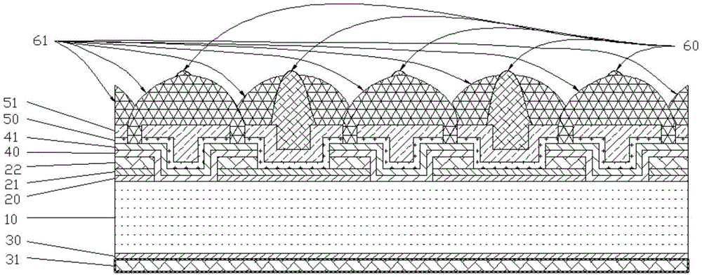
As shown in fig. 7-8, solder ribbon connection layers 60 are formed in an alternating spaced arrangement on the back side of the S4 silicon die 10. Fig. 7 is a cross-sectional view of the solder ribbon connection layer 60 formed on the back surface of the silicon wafer 10 and fig. 8 is a schematic structural view of the solder ribbon connection layer 60 formed on the back surface of the silicon wafer 10. The solder strip connecting layer 60 is weldable low-temperature silver paste, the thickness of the solder strip connecting layer is 10-15 micrometers, the length of the solder strip connecting layer is 5mm, the solder strip connecting layer is formed by baking for 20 minutes and curing at 190 ℃ after printing, and the solder strip connecting layer 60 is alternately arranged on the surfaces of the first semiconductor layer area 42 and the second semiconductor layer area 43 at intervals. Each row of the solder ribbon connection layers 60 perpendicular to the isolation trenches 53 corresponds to one main gate, and the solder ribbon connection layers 60 have 10 rows.
As shown in fig. 9-10, insulating layers 61 are formed on the back side of the S5 silicon wafer 10 alternating with solder ribbon connection layers 60. Fig. 9 is a cross-sectional view of the silicon wafer 10 with the alternately arranged insulating layers 61 formed on the back surface, and fig. 10 is a schematic structural view of the silicon wafer 10 with the alternately arranged insulating layers 61 formed on the back surface. The insulating layer 61 is formed by printing insulating ink and baking for 20 minutes at 150 ℃ for curing, the thickness of the insulating layer is 5-10um, the length is 6mm, the width is 0.5-0.8mm, and the insulating layer 61 and the welding strip connecting layer 60 are arranged alternately.
By adopting the technical scheme, the multi-main-grid structure of the back-contact heterojunction solar cell can be realized, the conductivity requirement of the solar cell piece on the thin grid line is remarkably reduced, meanwhile, the physical vapor deposition metal conducting layer is adopted as the thin grid electrode, and only the solder strip connecting layer adopts the conventional low-temperature silver paste, so that the unit consumption of the silver paste with the specification of G1 silicon wafer is reduced to 30-50mg, which is far lower than that of the silver paste with the specification of about 200mg of the conventional heterojunction. Meanwhile, the problems of copper-containing wastewater treatment, environmental protection, large production field, high operation cost and the like do not need to be considered when large-scale wet copper electroplating equipment is used, so that the production process flow of the cell is greatly simplified, the production cost is reduced, and the mass production and popularization of the back contact heterojunction solar cell with high conversion efficiency are facilitated.
The above description is only for the purpose of illustrating the preferred embodiments of the present invention and is not to be construed as limiting the utility model, and any modifications, equivalents and improvements made within the spirit and principle of the present invention are intended to be included within the scope of the present invention.