SUMMERY OF THE UTILITY MODEL
The embodiment of the utility model provides an LED chip structure, a display module and electronic equipment, which are used for solving the problem that the existing nanometer light-emitting diode cannot independently control nanometer LEDs with different diameters, so that full colorization cannot be realized.
To this end, according to a first aspect, an embodiment provides an LED chip structure comprising:
the LED column array is divided into different light emitting areas, the diameters of the nanometer LED columns in the same light emitting area are the same, and the diameters of the nanometer LED columns in the different light emitting areas are different; and
and the conductive electrode is electrically connected with each luminous area and supplies power to all the nano LED columns in each luminous area so as to realize that each luminous area is driven to emit light independently.
In some embodiments of the LED chip structure, the LED chip structure further includes a conductive layer and a passivation layer, the LED pillar array is disposed on the conductive layer, a surface of the conductive layer on a side away from the nano LED pillar is a light emitting surface, and the light emitting surface is roughened and then covered by the passivation layer.
In some embodiments of the LED chip structure, the LED chip structure further includes a separation groove and a light-blocking insulating partition, the LED pillar array is separated into different light-emitting areas by an insulating filler, the separation groove is disposed on the conductive layer and corresponds to the insulating filler, the separation groove is used to make the conductive layers of the light-emitting areas not connected with each other, and the light-blocking insulating partition is filled in the separation groove.
In some embodiments of the LED chip structure, the number of the light emitting regions is three, and the light emitting regions are a first light emitting region, a second light emitting region and a third light emitting region, and the diameters of the nano LED pillars in the first light emitting region, the second light emitting region and the third light emitting region are 150 nm-.
In some embodiments of the LED chip structure, the number of the conductive electrodes is at least one, and when the number of the conductive electrodes is plural, the conductive electrodes are uniformly distributed or symmetrically distributed.
In some embodiments of the LED chip structure, passivation is filled between the nano LED pillars in the same light emitting region.
In some embodiments of the LED chip structure, the insulating filler is a transparent insulating filler, an opaque insulating filler or a reflective insulating filler, and the passivation is a transparent insulating material.
In some embodiments of the LED chip structure, the LED chip structure is a flip chip structure or a vertical chip structure.
According to a second aspect, an embodiment provides a display module comprising the LED chip structure according to the first aspect of the utility model.
According to a third aspect, an embodiment provides an electronic device including the display module according to the second aspect of the utility model.
The embodiment of the utility model has the following beneficial effects:
according to the LED chip structure, the display module and the electronic device in the embodiment, the LED column array formed by the nanometer LED columns is divided into different light emitting areas by the LED chip structure, the nanometer LED columns in the different light emitting areas have different sizes, the light emitting areas are independently and electrically connected with the conductive electrodes, the full colorization of the chip is realized by independently controlling the nanometer LED columns in the light emitting areas by utilizing the size effect of the nanometer LED columns, and compared with the structure of RGB (red, green and blue) three-primary-color synthesis and UV/blue light excitation quantum dots, the structure is simple to prepare, does not need color conversion materials, and has obvious advantages. The display module and the electronic equipment have the advantages of low cost and more bright color due to the adoption of the LED chip structure.
Detailed Description
To facilitate an understanding of the utility model, the utility model will now be described more fully with reference to the accompanying drawings. Preferred embodiments of the present invention are shown in the drawings. The utility model may, however, be embodied in many different forms and should not be construed as limited to the embodiments set forth herein. Rather, these embodiments are provided so that this disclosure will be thorough and complete.
It will be understood that when an element is referred to as being "secured to" another element, it can be directly on the other element or intervening elements may also be present. When an element is referred to as being "connected" to another element, it can be directly connected to the other element or intervening elements may also be present. The terms "vertical," "horizontal," "left," "right," and the like as used herein are for illustrative purposes only.
Unless defined otherwise, all technical and scientific terms used herein have the same meaning as commonly understood by one of ordinary skill in the art to which this invention belongs. The terminology used in the description of the utility model herein is for the purpose of describing particular embodiments only and is not intended to be limiting of the utility model. As used herein, the term "and/or" includes any and all combinations of one or more of the associated listed items.
Embodiments of the present invention provide an LED chip structure, which in one embodiment, as shown in fig. 13 to 14, includes a conductive layer 31, an LED pillar array, a separation groove 34, and a conductive electrode 100.
The LED column array is composed of a plurality of nanometer LED columns 40 formed on a conducting layer 31, the nanometer LED columns 40 are of a semiconductor structure, the LED column array is divided into different light emitting areas by insulating fillers 60, each light emitting area comprises at least two nanometer LED columns 40, the diameters of the nanometer LED columns 40 in the same light emitting area are the same, and the diameters of the nanometer LED columns 40 in the different light emitting areas are different.
It should be noted that the nano LED pillar 40 is a semiconductor structure, and includes a second N-type layer 32, an active layer 41, and a P-type layer 42 sequentially stacked on a first N-type layer, where the conductive layer 31 is the first N-type layer.
The separation groove is disposed on the conductive layer 31 and corresponds to the insulating filler 60, and the separation groove 34 is used to prevent the conductive layers 31 of the light emitting regions from being connected to each other.
The conductive electrodes 100 are respectively disposed in the light emitting areas, the conductive electrodes 100 in the light emitting areas are electrically connected to the conductive layer 31 in the light emitting areas, and the conductive electrodes 100 supply power to all the nano LED pillars 40 in the light emitting areas, so that the light emitting areas can emit light by independent electric driving.
Specifically, the LED pillar array may be a regular array, such as N rows, M columns, or concentric circles, or may be an irregular array, preferably a regular array, which is beneficial to the uniform distribution of the nano LED pillars 40 in each light emitting region, so as to provide uniform light emitting color.
In the embodiment of the utility model, the LED chip structure divides the LED column array formed by the nanometer LED columns 40 into different light emitting areas through the insulating filler 60, the nanometer LED columns 40 in the different light emitting areas have different sizes, the separation groove 34 is arranged on the conducting layer 31 to electrically isolate the light emitting areas, the conducting layer 31 of each light emitting area is provided with the conducting electrode 100, the full colorization of the chip is realized by independently controlling the nanometer LED columns 40 in each light emitting area by utilizing the size effect of the nanometer LED columns 40, and compared with the structure of RGB three-primary-color synthesis and UV/blue light excitation quantum dots, the structure is simple to prepare, does not need color conversion materials, and has obvious advantages.
It should be noted that, in a specific embodiment, as shown in fig. 13, the LED chip structure further includes a P electrode 80, and the P electrode 80 is electrically connected to the P-type layers 42 of all the nano LED pillars 40 in all the light emitting areas, that is, the P electrode 80 is shared by all the light emitting areas, which is beneficial to batch preparation of the P electrode 80 and simplification of the preparation process of the P electrode 80, and the P electrode 80 may be any P electrode 80 structure in the prior art, which is not limited herein.
Further, the P-electrode 80 includes a metal layer 81 laminated on all the nano LED pillars 40 of all the light emitting areas, the insulating filler 60 and the passivation 70, and a conductive substrate 82 bonded to the metal layer 81, the metal layer 81 is electrically connected to the P-type layers 42 of all the nano LED pillars 40 of all the light emitting areas, and the conductive substrate 82 can provide heat dissipation for the metal layer 81, improve current uniformity, reduce internal resistance, and improve the overall heat dissipation and low power consumption of the device.
Specifically, the conductive substrate 82 may be a silicon substrate, a copper substrate, or the like.
In a specific embodiment, as shown in fig. 13, the LED chip structure further includes a passivation layer 35, a surface of the conductive layer 31 facing away from the nano LED pillar 40 is a light emitting surface 33, and the light emitting surface 33 is covered by the passivation layer 35 after being roughened.
Specifically, the passivation layer 35 is preferably a transparent insulating material, such as silicon dioxide, silicon nitride, or the like, which does not affect light emission.
In a specific embodiment, as shown in fig. 13, the LED chip structure further includes a light-blocking insulating spacer 61, and the light-blocking insulating spacer 61 is filled in the separation groove 34.
Specifically, the light-blocking insulating partition 61 is made of a light-impermeable and insulating material, and the light-blocking insulating partition 61 is filled in the separation groove 34 to form a light-blocking wall, preventing the occurrence of light crosstalk between the light-emitting regions.
In a specific embodiment, as shown in fig. 13-14, the number of the light emitting regions is three, which are the first light emitting region 51, the second light emitting region 52 and the third light emitting region 53, and the diameters of the nano LED pillars 40 in the first light emitting region 51, the second light emitting region 52 and the third light emitting region 53 are respectively 100-.
It can be understood that the nano LED pillars 40 of different diameters emit light of different wavelengths according to the size effect of the nano LED pillars 40. The nano LED column 40 with the diameter of 100-. The input currents of the three light emitting areas are separately controlled, and full-color display can be realized.
Of course, in other embodiments, there may be two light emitting regions or more than three light emitting regions. Of course, the diameter of the nano LED pillar 40 in each light emitting region may have other specifications, and is not limited herein.
In a specific embodiment, as shown in fig. 13-14, the conductive electrode 100 is disposed for each light emitting region, and since the light emitting region includes a plurality of nano LED pillars 40, the size of the conductive electrode 100 is not necessarily too small, thereby reducing the difficulty of the process. The number of the conductive electrodes 100 in each light emitting area is at least 1, and when the number of the conductive electrodes 100 is plural, the conductive electrodes 100 are uniformly or symmetrically distributed, for example, the number of the conductive electrodes 100 may be 1, 2 or more than 2, and when the number of the conductive electrodes 100 is greater than or equal to 2, the conductive electrodes 100 may be symmetrically distributed about a central axis or a symmetry axis of the light emitting area, may be uniformly distributed about the central axis of the light emitting area, or may be uniformly distributed on the light emitting area, and since the conductive electrodes 100 supply power to all the nano LED pillars 40 in the light emitting area, the conductive electrodes 100 are uniformly or symmetrically distributed, and uniformity of current distributed to the nano LED pillars 40 may be improved.
As shown in fig. 14, in the present embodiment, the number of the conductive electrodes 100 in each light emitting region is two, and the conductive electrodes are respectively disposed at both ends of each light emitting region.
In one particular embodiment, the gaps between the nano-LED pillars 40 are filled with a passivation 70, as shown in fig. 13.
Specifically, the passivation 70 is preferably a transparent insulating material, such as silicon dioxide, silicon nitride, etc., which does not affect light extraction.
In some embodiments, the insulating filler 60 is a transparent insulating filler, an opaque insulating filler, or a reflective insulating filler, and the passivation 70 is a transparent insulating material.
Specifically, when the insulating filler 60 is a transparent insulating filler, the material of the transparent insulating filler may be silicon dioxide, silicon nitride, or the like, which also has a function of passivating the sidewalls of the nano LED pillar 40.
When the insulating filler 60 is an opaque insulating filler, the material of the opaque insulating filler may be an opaque resin material or the like.
When insulating filler 60 is reflection of light insulating filler, reflection of light insulating filler includes the metal reflection of light main part and the printing opacity insulating layer of the side and the bottom surface of cladding metal reflection of light main part, the bottom in clearance contacts between printing opacity insulating layer and the lateral wall of nanometer LED post 40 and the adjacent nanometer LED post 40, can electrically insulated between messenger nanometer LED post 40 and the metal reflection of light main part, the metal reflection of light main part is with light reflex each luminous zone again, avoid the not light of the co-chromatic light in adjacent luminous zone to produce the phenomenon of crosstalk, influence each other.
Wherein the material of the metal light reflecting main body can be aluminum, gold and other materials,
the preparation method of the reflective insulation filler can be as follows: a light-transmitting insulating layer is formed on the bottom of the gap between some of the nano LED pillars 40 of the provided substrate and the sidewall of the nano LED pillars 40, and then a metal light-reflecting body is continuously formed on the light-transmitting insulating layer to fill the gap between the nano LED pillars 40, thereby forming a light-reflecting insulating filler filled in the gap between some of the nano LED pillars 40. The method of forming the light-transmitting insulating layer may be a sputtering method or a deposition method, and the method of forming the metal light-reflecting body may also be a sputtering method or a deposition method.
Of course, in other embodiments, the insulating filler 60 may be an air layer, and the air layer may also have an insulating effect.
In order to further simplify the process, the conductive layer 31 and the second N-type layer 32 may be made of the same material, or may be made of different materials, in this embodiment, since the LED pillar array is obtained by etching an epitaxial wafer, the conductive layer 31 and the second N-type layer 32 are made of the same material.
In a specific embodiment, the nano LED pillar 40 further includes a current spreading layer 43 laminated to a side of the P-type layer 42 away from the N-type layer 30, and the current spreading layer 43 can improve current spreading between the nano LED pillar 40 and the P-electrode 80, reduce internal resistance, and improve device performance.
The LED chip structure of each of the above embodiments may be a flip chip structure, or may be a vertical chip structure, where the flip chip structure is the same side as the P electrode 80 and the conductive electrode 100, and the vertical chip structure is different sides of the P electrode 80 and the conductive electrode 100, and the conductive electrode 100 of the vertical chip structure is disposed on the side of the conductive layer 31 away from the LED pillar.
Taking the preparation of a vertical chip structure as an example, the following provides a preparation method of an LED chip structure, and the method comprises the following steps:
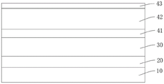
and S1, preparing an epitaxial wafer. On a substrate 10 (silicon substrate, sapphire, SiC, GaN, etc.), a buffer layer 20, an N-type layer 30 of GaN, an active layer 41 of InGaN/GaN blue light multiple quantum well, and a P-type layer 42 of GaN are sequentially grown to obtain a blue LED epitaxial material, and the structure of the epitaxial wafer is shown in fig. 1.
S2, preparing an LED column array. Three nano LED columns 40 with different sizes are prepared step by adopting a zone preparation method.
The method comprises the following specific steps: a current spreading layer 43 is deposited on the P-type layer 42 of the LED epitaxial wafer, and thermal annealing treatment is performed. Depositing a hard thin film layer (such as silicon dioxide, silicon nitride and the like) on the upper surface of the current spreading layer 43, making the lower surface of the hard mask in contact with the current spreading layer 43, preparing a plurality of auxiliary nano patterns on the upper surface of the hard thin film layer, and etching the current spreading layer 43 through the auxiliary nano patterns to form a plurality of masks; and etching the epitaxial wafer by using the patterned mask layer as a mask until a plurality of nano LED columns 40 are formed inside the N-type layer 30, as shown in FIG. 2. The diameters of the nanometer LED column 40 are respectively 100-150nm, 151-200nm and 201-300 nm.
And S3, passivating the side wall of the nanometer LED pillar 40. And (3) placing the nano LED column 40 in a KOH solution of 1mol/L at 80 ℃ for soaking for 5-10mins, removing the side wall damage layer, and then cleaning with an HCl solution.
S4, insulating filler 60, and passivation 70. Appropriate amounts of insulating fillers 60 and passivation 70 (transparent insulating oxide or nitride such as SiO2 and SiNx) are sequentially filled in the gaps of the nano LED pillars 40, as shown in fig. 3.
S5, depositing metal layer 81. A metal layer 81 (e.g., Ni/Ag, Ti/Al/Ti/Au, etc.) having a reflective function is deposited on the ITO and passivation film of the nano LED pillar 40 by electron beam evaporation, as shown in fig. 4.
And S6, bonding the substrates. The metal layer 81 is bonded to a conductive substrate 82 (e.g., a silicon substrate, a copper substrate, etc.) to form a P-electrode 80, as shown in fig. 5.
S7, substrate 10 and buffer layer 20 are removed. The substrate 10 and buffer layer 20 are removed by laser lift-off, mechanical polishing, chemical etching or a combination thereof to leak the N-type layer 30, as shown in fig. 6.
S8, the light emitting surface 33 is roughened. The surface of the conductive layer 31 on the side away from the nano LED pillar 40 is roughened by hot KOH solution to form a hexagonal cone shape, so as to reduce total reflection of light and improve light extraction efficiency, as shown in fig. 7.
S9, manufacturing the separation groove 34. The separation grooves 34 are formed on the roughened surface by wet etching, dry etching, dicing with a dicing saw, etc., in preparation for electrical separation between different light-emitting areas, as shown in fig. 8.
S10, passivation layer 35 deposition. The electrical separation of the chips from group to group is achieved by depositing a passivation layer 35(SiO2, Si3N4, Al2O3, etc.) on the chip surface and in the separation grooves 34 using PECVD (plasma enhanced chemical vapor deposition) or ALD (atomic layer deposition technique), as shown in fig. 9.
And S11, removing the material in the separation groove 34. After the photolithography development, the passivation layer 35 in the separation groove 34 is removed by a dry etching (e.g., ICP, RIE, etc.) or a wet etching (BOE solution), as shown in fig. 10.
S12, preparing a light blocking wall. The separation grooves 34 are filled with light blocking insulating spacers 61 to prevent the occurrence of optical crosstalk, as shown in fig. 11.
S13, opening a hole in passivation layer 35 to expose conductive layer 31 for depositing conductive electrode 100. And sequentially spin-coating adhesive and photoresist 90 on the passivation layer 35, and removing the passivation layer 35 in the corresponding region by exposure, development, dry etching or wet etching. The device was placed in an RIE (reactive ion etching) chamber and bombarded at 100W power for 5-10mins, as shown in fig. 12.
S14, forming the conductive electrode 100. The conductive electrode 100 may be formed at the opening by evaporation using an electron beam evaporation technique. In this embodiment, the conductive electrode 100 is a Cr/Pt/Au composite layer, as shown in FIG. 13, and the top view of the resulting LED chip structure is shown in FIG. 14.
The utility model also discloses a display module comprising the LED chip structure. The display module can be applied to mobile phones, flat panels, notebook computers, televisions, AR/VR equipment, vehicle instruments, central control, outdoor displays, head-up displays (HUDs) and other products.
The utility model also discloses electronic equipment comprising the display module, wherein the electronic equipment can be a mobile phone, a tablet, a notebook computer, a television, AR/VR equipment, a vehicle instrument and central control, an outdoor display, a head-up display (HUD) and the like.
The technical features of the above embodiments can be arbitrarily combined, and for the sake of brevity, all possible combinations of the technical features in the above embodiments are not described, but should be considered as the scope of the present specification as long as there is no contradiction between the combinations of the technical features.
The above examples only show some embodiments of the present invention, and the description thereof is more specific and detailed, but not construed as limiting the claims. It should be noted that, for a person skilled in the art, several variations and modifications can be made without departing from the inventive concept, which falls within the scope of the present invention. Therefore, the protection scope of the present patent shall be subject to the appended claims.