CN213984938U - Jig and testing device - Google Patents
Jig and testing device Download PDFInfo
- Publication number
- CN213984938U CN213984938U CN202023203872.8U CN202023203872U CN213984938U CN 213984938 U CN213984938 U CN 213984938U CN 202023203872 U CN202023203872 U CN 202023203872U CN 213984938 U CN213984938 U CN 213984938U
- Authority
- CN
- China
- Prior art keywords
- main body
- jig
- base
- tested
- product
- Prior art date
- Legal status (The legal status is an assumption and is not a legal conclusion. Google has not performed a legal analysis and makes no representation as to the accuracy of the status listed.)
- Active
Links
- 238000012360 testing method Methods 0.000 title claims abstract description 53
- 230000003287 optical effect Effects 0.000 claims abstract description 44
- 238000000034 method Methods 0.000 abstract description 5
- 230000008569 process Effects 0.000 abstract description 5
- 238000013095 identification testing Methods 0.000 abstract description 3
- 230000000149 penetrating effect Effects 0.000 abstract description 2
- 238000005516 engineering process Methods 0.000 description 2
- 238000001310 location test Methods 0.000 description 2
- 238000004519 manufacturing process Methods 0.000 description 2
- 238000012545 processing Methods 0.000 description 2
- 230000003321 amplification Effects 0.000 description 1
- 238000004364 calculation method Methods 0.000 description 1
- 238000004891 communication Methods 0.000 description 1
- 238000013461 design Methods 0.000 description 1
- 238000001514 detection method Methods 0.000 description 1
- 238000011161 development Methods 0.000 description 1
- 238000006073 displacement reaction Methods 0.000 description 1
- 238000012986 modification Methods 0.000 description 1
- 230000004048 modification Effects 0.000 description 1
- 238000003199 nucleic acid amplification method Methods 0.000 description 1
- 238000003908 quality control method Methods 0.000 description 1
- 239000004065 semiconductor Substances 0.000 description 1
Images


Landscapes
- Investigating Materials By The Use Of Optical Means Adapted For Particular Applications (AREA)
Abstract
The utility model relates to a test tool technical field, concretely relates to tool and testing arrangement. The testing device comprises an optical image tester and a jig, the jig is fixed on the optical image tester and comprises a base, a platform used for placing a product to be tested is formed on the front side of the base, and the jig is further provided with a hollow part penetrating through the back side of the base and the platform, so that the optical image tester can identify and test the position of the product to be tested through the hollow part. The jig is fixed on the optical image tester so as to be matched with the optical image tester to carry out positioning test on a product to be tested, during testing, the product to be tested is placed on a platform on the front side of the base, then the optical image tester is used for obtaining and judging the position information of the product to be tested through the hollow part from the back side of the base, so that the identification test of the position of the product to be tested is completed, the position precision of the product to be tested in the assembling process is ensured, and the horizontal placement of the product to be tested is ensured through the platform.
Description
Technical Field
The utility model relates to a test tool technical field, concretely relates to tool and testing arrangement.
Background
Nowadays, with the rapid development of semiconductor technology, chips with different predetermined functions are increasingly applied to electronic products such as mobile phones, computers and the like, so that people's lives are more and more convenient.
In the production process of electronic products, the chip needs to be assembled, and because the chip has a high requirement on the position precision during the assembly, usually more than 10 micrometers, an optical image tester is generally used for testing the position of the chip, wherein a jig for placing the chip so as to test the chip plays an important role in the test process. Therefore, it is necessary to design a jig, which can be combined with an optical image tester to form a testing device for positioning and testing a chip, so as to ensure the position accuracy of the chip during assembly.
SUMMERY OF THE UTILITY MODEL
The utility model discloses a main objective is: the jig can be matched with an optical image tester to form a testing device for positioning and testing a chip, and the position precision of the chip in the assembling process is ensured.
In order to realize the technical problem, the utility model provides a tool, tool is used for fixing on the optics image tester, tool includes the base, the base openly is formed with the platform that is used for placing the product that awaits measuring, tool still has and link up the base back with the fretwork portion of platform, so that the optics image tester passes through fretwork portion is right the position of the product that awaits measuring discerns the test.
Optionally, the hollow portions are arranged around the outer contour of the product to be tested and penetrate through the plurality of hollow holes of the platform from the back of the base.
Optionally, the jig further comprises a fixing member, the fixing member is disposed on the base, and the fixing member is used for fixing the product to be tested on the base.
Optionally, the fixing member is provided with a plurality of outer contours surrounding the product to be tested, and the hollow holes and the fixing member are alternately arranged.
Optionally, the jig further comprises a limiting seat, wherein the limiting seat is fixedly arranged on the platform of the base and provided with a limiting hole for limiting the position of the product to be tested.
Optionally, the jig includes a first main body portion and a second main body portion connected to each other, the first main body portion is used for being fixed on the optical image tester, and the second main body portion includes the base and the hollow portion.
Optionally, the second body portion is detachably connected to the first body portion.
Optionally, the first main body portion has a first surface and a second surface perpendicular to each other, and the second main body portion is connected to the first main body portion through the first surface and the second surface in a positioning manner;
the jig further comprises a magnetic part, and the second main body part is connected with the first main body part through the magnetic part.
Optionally, the first body part has a first coordinate mark, and the second body part has a second coordinate mark;
the second main body part is also provided with a test identification point.
Additionally, the utility model provides a testing arrangement, testing arrangement include optics image tester and as above-mentioned arbitrary one the tool, the tool is fixed on the optics image tester.
The utility model has the advantages that: the jig is fixed on the optical image tester so as to be matched with the optical image tester to carry out positioning test on the product to be tested. During testing, a product to be tested is placed on the platform on the front side of the base, and then the optical image tester is used for obtaining and judging the position information of the product to be tested from the back side of the base through the hollow part so as to complete the identification test of the position of the product to be tested and ensure the position precision of the product to be tested during assembling. In addition, the horizontal placement of the products to be tested is ensured by arranging the platform.
Drawings
The above and/or additional aspects and advantages of the present invention will become apparent and readily appreciated from the following description of the embodiments, taken in conjunction with the accompanying drawings of which:
fig. 1 is a top view of the jig and the chip of the present invention;
FIG. 2 is a top view of the second body portion and the chip of the fixture of FIG. 1;
FIG. 3 is a cross-sectional view taken along A-A of FIG. 2;
FIG. 4 is a top view of a portion of the second body portion of FIG. 2;
FIG. 5 is a cross-sectional view taken along line B-B of FIG. 4;
FIG. 6 is a top view of the retainer of the second body portion of FIG. 2;
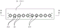
wherein the correspondence between the reference numbers and the names of the components in fig. 1 to 6 is:
100. a jig;
10. a first main body portion; 11. a first side; 12. a second face; 13. a first coordinate identification;
20. a second main body portion; 21. a base; 211. a platform; 212. hollowing out holes; 213. placing holes; 214. an empty avoiding groove; 22. a fixing member; 23. a limiting seat; 231. a limiting hole; 232. a second coordinate identification; 233. testing the identification points;
200. and (3) a chip.
Detailed Description
In order to make the aforementioned objects, features and advantages of the present invention more clearly understood, the present invention will be described in further detail with reference to the accompanying drawings and detailed description. It should be noted that the embodiments and features of the embodiments of the present application may be combined with each other without conflict.
In the description of the present invention, it should be noted that the terms "upper", "lower", and the like indicate orientations or positional relationships based on the orientations or positional relationships shown in the drawings, which are only for convenience of description and simplification of description, but do not indicate or imply that the device or element referred to must have a specific orientation, be constructed in a specific orientation, and be operated, and thus, should not be construed as limiting the present invention. Furthermore, the terms "first" and "second" are used for descriptive purposes only and are not to be construed as indicating or implying relative importance.
In the description of the present invention, it is to be noted that, unless otherwise explicitly specified or limited, the terms "mounted," "connected," and "connected" are to be construed broadly, and may be, for example, fixedly connected, detachably connected, or integrally connected; can be mechanically or electrically connected; the communication may be direct, indirect via an intermediate medium, or internal to both elements. The specific meaning of the above terms in the present invention can be understood in specific cases to those skilled in the art. In addition, in the description of the present invention, "a plurality" means two or more unless otherwise specified.
An embodiment of the utility model provides a carry out tool 100 of optics image testing arrangement, this tool 100 can cooperate optics image tester to carry out the location test to the product that awaits measuring, guarantees the position precision of the product that awaits measuring when the equipment, and the product that wherein awaits measuring can be chip 200, explains below with can fix chip 200 and then carry out the tool 100 of location test to chip 200 as the example. As shown in fig. 1 to 6, the fixture 100 is fixed on the optical image tester, the fixture 100 includes a base 21, a platform 211 for placing the chip 200 is formed on the front surface of the base 21, and the fixture 100 further has a hollow portion penetrating the back surface of the base 21 and the platform 211, so that the optical image tester can perform a recognition test on the position of the chip 200 through the hollow portion.
In the above-mentioned jig 100, the jig 100 is fixed on the optical image tester, so as to cooperate with the optical image tester to perform the positioning test on the chip 200. During testing, the chip 200 is placed on the platform 211 on the front surface of the base 21, and then the optical image tester is used for obtaining and judging the position information of the chip 200 from the back surface of the base 21 through the hollow part, so that the identification test of the position of the chip 200 is completed, and the position accuracy of the chip 200 during assembling is ensured. In addition, the platform 211 is arranged to ensure that the chip 200 is horizontally placed.
Since the chip 200 is required to have a high positional accuracy, usually 10 μm or more, during assembly, the position of the chip 200 is generally measured using an optical image tester. The optical image tester is a high-precision, high-efficiency and high-reliability measuring instrument integrating optical, mechanical, electronic and computer image processing technologies, the optical image tester amplifies a chip 200 by an optical amplification system, acquires image characteristics of the chip 200 by a CCD camera system and sends the image characteristics to a computer, and the computer can quickly read the displacement value of an optical ruler and instantly obtain a required result by the operation of a software module established on the basis of space geometry, so that the contour, the surface shape, the size, the angle and the position of the chip 200 can be efficiently detected, and microscopic detection and quality control can be performed. In the testing process of the optical image tester, the jig 100 can be used to carry the chip 200 to test whether the chip 200 is located at the position where the platform 211 should be located, and then the chip 200 is assembled to ensure the position accuracy of the chip 200 during the assembly.
In the present embodiment, the fixture 100 includes a first main body 10 and a second main body 20 connected to each other, the first main body 10 is fixed on the optical image tester, and the second main body 20 has a base 21 and a hollow portion. That is, in the present embodiment, the jig 100 is formed by combining two parts, namely, a first main body 10 and a second main body 20, the first main body 10 is fixedly mounted on the optical image tester by screws, the second main body 20 is mounted on the first main body 10 and is used for placing the chip 200, and then the position of the chip 200 on the platform 211 can be tested by the optical image tester.
In the present embodiment, the hollow portions are disposed around the outer contour of the chip 200 and penetrate from the back surface of the base 21 to the plurality of hollow holes 212 of the platform 211. Specifically, in the present embodiment, the stage 211 is provided with a placement hole 213 for passing a part of the structure of the chip 200. During testing, one end of the columnar chip 200 penetrates through the placing hole 213, the other end of the chip 200 is clamped above the platform 211 through the convex edge, then the optical image tester is used for identifying the outline of the chip 200 through the plurality of hollow holes 212 from the back of the base 21 in a backlight mode, and data such as position information of the chip 200 are obtained through calculation, so that whether the chip 200 is located at the position where the platform 211 should be located or not is accurately judged. In addition, in this embodiment, the center of the back of the base 21 is provided with the clearance groove 214, so as to realize clearance on the one hand and facilitate placement of the chip 200, and on the other hand, facilitate hollowing out, facilitate production and processing of the whole jig 100, and reduce the dead weight of the whole jig 100.
In this embodiment, the second main body 20 further includes a fixing member 22, the fixing member 22 is disposed on the base 21, and the fixing member 22 is used for fixing the chip 200 on the base 21, preferably, the fixing member 22 is a magnetic block. Through setting up mounting 22, when placing chip 200 on the positive platform 211 of base 21, the protruding edge of chip 200 card above platform 211 passes through mounting 22 fastening on platform 211, can avoid in the test process, and chip 200 takes place to remove relative base 21, leads to optical image tester position test deviation to appear, influences the test result. In addition, the chip 200 is fixed on the base 21 by the magnetic block, that is, the chip 200 is fixed, so that the chip 200 is in close contact with the base 21, and the magnetic block fixing structure is simple and low in cost. Of course, in other embodiments, the fixing member 22 may be fixed in other manners.
Further, in the present embodiment, the fixing elements 22 are disposed in a plurality around the outer contour of the chip 200, and the hollow holes 212 and the fixing elements 22 are alternately disposed. Like this, not only optical image tester can follow the base 21 back and see through a plurality of fretwork holes 212 that evenly set up and be shaded from the sun and discern a plurality of identification points on the chip 200 outline, and then discern the whole outline image positioning of chip 200, and a plurality of mountings 22 that whole chip 200 accessible evenly set up are firmly fastened on base 21 moreover, further guarantee optical image tester to the precision of placing the chip 200 position test on platform 211.
In this embodiment, the second main body 20 further includes a limiting seat 23, and the limiting seat 23 is fixedly disposed on the platform 211 of the base 21 and is provided with a limiting hole 231 for limiting the position of the chip 200. Through setting up spacing seat 23, the position on base 21 is placed to chip 200 to spacing hole 231 on the spacing seat 23 of accessible is injectd tentatively, nevertheless because chip 200 is spacing to have certain deviation through spacing hole 231, then carries out accurate discernment test, easy operation, the test of being convenient for to chip 200's position through the optics image tester again.
In this embodiment, the second body portion 20 is detachably connected to the first body portion 10. That is, in the present embodiment, the first main body 10 is fixedly mounted on the optical image tester by screws, and the second main body 20 is movably mounted on the first main body 10 and is used for placing the chip 200. Because the second main body part 20 is detachably connected with the first main body part 10, the second main body part 20 can be freely taken and placed, and the chip 200 can be conveniently clamped. During testing, the second main body portion 20 may be detached from the first main body portion 10, the chip 200 may be fixed on the second main body portion 20, and then the chip 200 and the second main body portion 20 may be mounted on the first main body portion 10. Of course, in other embodiments, the second body portion 20 and the first body portion 10 may be integrally formed.
Further, in this embodiment, the first main body 10 has a first surface 11 and a second surface 12 perpendicular to each other, the second main body 20 is connected to the first main body 10 through the first surface 11 and the second surface 12, the jig 100 further includes a magnetic member, and the second main body 20 is connected to the first main body 10 through the magnetic member. Specifically, in the present embodiment, the first body portion 10 has an L-shape, the second body portion 20 has a rectangular parallelepiped shape, and the second body portion 20 having the rectangular parallelepiped shape is positioned by the first surface 11 and the second surface 12 of the L-shaped first body portion 10, which are located at the inner side and perpendicular to each other, so that the positional accuracy of the second body portion 20 when the second body portion is mounted on the first body portion 10 is ensured. In addition, the first main body part 10 and the second main body part 20 are magnetically attracted to achieve the attraction and positioning, so that the structure is simple, and the second main body part 20 can be detached at will, thereby facilitating the test. Of course, in other embodiments, the detachable connection manner of the second body portion 20 and the first body portion 10 is not limited to magnetic attraction.
In this embodiment, the first main body 10 has a first coordinate mark 13, the second main body 20 has a second coordinate mark 232, the optical image tester performs recognition test on the position of the chip 200 through the plurality of hollow holes 212 according to the first coordinate mark 13 and the second coordinate mark 232, the second coordinate mark 232 is located on the limit seat 23, and preferably, both the first coordinate mark 13 and the second coordinate mark 232 are XY coordinate marks. Specifically, during testing, the optical image tester may integrate according to the first coordinate identifier 13 and the second coordinate identifier 232, and the finally tested XY data is directly connected to the parameters set by the optical image tester to obtain the result of the position test of the chip 200. In addition, for different assembly stations, when the positioning test of the chip 200 is performed, the second coordinate marks 232 on the second main body portion 20 are not completely the same, so that the positioning test requirements of different assembly stations can be met according to actual conditions.
Further, in this embodiment, the second main body portion 20 further has a test identification point 233, and the test identification point 233 is located on the limiting seat 23. Because the second main body part 20 is provided with the test identification point 233, the test identification point 233 can be used as a reference point when the chip 200 is tested, so that the optical image tester can successfully find a plurality of points on the outer contour of the chip 200, and further recognize the image information of the whole outer contour for judgment, thereby effectively improving the test efficiency of the optical image tester.
In addition, in this embodiment, a plurality of chips 200 can be placed on the platform 211 at the same time, so that the jig 100 can be combined with an optical image tester to perform batch high-precision testing on the plurality of chips 200 at the same time, wherein data to be tested includes the position of each chip 200, the distance between any two adjacent chips 200, and the like, and the spacing seat 23 can ensure the placing consistency of each chip 200 and the distance consistency between any two adjacent chips 200.
The above description is only for the preferred embodiment of the present invention, and is not intended to limit the present invention, and any modifications, equivalent replacements, improvements, etc. made within the spirit and principle of the present invention should be included within the protection scope of the present invention.
Claims (10)
1. The fixture is characterized by being fixed on an optical image tester and comprising a base, wherein a platform for placing a product to be tested is formed on the front side of the base, and the fixture is also provided with a hollow part which penetrates through the back side of the base and the platform, so that the optical image tester identifies and tests the position of the product to be tested through the hollow part.
2. The jig of claim 1, wherein: the hollow parts are arranged around the outline of the product to be tested and penetrate through the back face of the base to the plurality of hollow holes of the platform.
3. The jig of claim 2, wherein: the fixture further comprises a fixing piece, the fixing piece is arranged on the base, and the fixing piece is used for fixing the product to be tested on the base.
4. The jig of claim 3, wherein: the fixing piece encircles the outline of the product to be tested is provided with a plurality of, just the fretwork hole with the fixing piece sets up in turn.
5. The jig of claim 3, wherein: the jig further comprises a limiting seat, wherein the limiting seat is fixedly arranged on the platform of the base and is provided with a limiting hole for limiting the position of the product to be tested.
6. The jig according to any one of claims 1 to 5, characterized in that: the jig comprises a first main body part and a second main body part which are connected, the first main body part is used for being fixed on the optical image tester, and the second main body part is provided with the base and the hollow part.
7. The jig of claim 6, wherein: the second main body part is detachably connected with the first main body part.
8. The jig of claim 7, wherein: the first main body part is provided with a first surface and a second surface which are perpendicular to each other, and the second main body part is positioned and connected with the first main body part through the first surface and the second surface;
the jig further comprises a magnetic part, and the second main body part is connected with the first main body part through the magnetic part.
9. The jig of claim 8, wherein: the first main body part is provided with a first coordinate mark, and the second main body part is provided with a second coordinate mark;
the second main body part is also provided with a test identification point.
10. A testing apparatus, comprising an optical image tester and the jig of any one of claims 1 to 9, wherein the jig is fixed on the optical image tester.
Priority Applications (1)
| Application Number | Priority Date | Filing Date | Title |
|---|---|---|---|
| CN202023203872.8U CN213984938U (en) | 2020-12-25 | 2020-12-25 | Jig and testing device |
Applications Claiming Priority (1)
| Application Number | Priority Date | Filing Date | Title |
|---|---|---|---|
| CN202023203872.8U CN213984938U (en) | 2020-12-25 | 2020-12-25 | Jig and testing device |
Publications (1)
| Publication Number | Publication Date |
|---|---|
| CN213984938U true CN213984938U (en) | 2021-08-17 |
Family
ID=77248335
Family Applications (1)
| Application Number | Title | Priority Date | Filing Date |
|---|---|---|---|
| CN202023203872.8U Active CN213984938U (en) | 2020-12-25 | 2020-12-25 | Jig and testing device |
Country Status (1)
| Country | Link |
|---|---|
| CN (1) | CN213984938U (en) |
-
2020
- 2020-12-25 CN CN202023203872.8U patent/CN213984938U/en active Active
Similar Documents
| Publication | Publication Date | Title |
|---|---|---|
| JP7465854B2 (en) | Test Carrier | |
| US6794889B2 (en) | Unified apparatus and method to assure probe card-to-wafer parallelism in semiconductor automatic wafer test, probe card measurement systems, and probe card manufacturing | |
| US6396296B1 (en) | Method and apparatus for electrical characterization of an integrated circuit package using a vertical probe station | |
| KR100221951B1 (en) | Test part of ic handler | |
| CN102207370A (en) | Assembly inspection apparatus and assembly processing apparatus using the same | |
| JP5464468B2 (en) | Substrate inspection device and inspection jig | |
| CN111486787A (en) | Test positioning method and test positioning system | |
| JP7109856B1 (en) | test carrier | |
| KR101358564B1 (en) | Probe card positioning mechanism and inspection apparatus | |
| CN213984938U (en) | Jig and testing device | |
| US7057408B2 (en) | Method and prober for contacting a contact area with a contact tip | |
| JP2002365310A (en) | Vertical-type probe card | |
| CN220085383U (en) | Intelligent hole pin assembly augmented reality device | |
| CN111014970A (en) | Lens optical path inspection tooling | |
| US20020050042A1 (en) | Docking system for connecting a tester to a probe station using an A-type docking configuration | |
| CN211219191U (en) | Lens light path detects frock | |
| WO2003037575A2 (en) | Method of calibrating a component placement machine, device suitable for carrying out such a method, and calibration component suitable for use in such a method or device | |
| CN209044015U (en) | A kind of high-precision quasi core piece design analytical equipment | |
| CN220260799U (en) | Clamp and robot flexibility detection equipment | |
| CN223742673U (en) | No-load test system for single-station motor | |
| CN108020361A (en) | Stress test gauge and mainboard stacking pressure test system | |
| CN220271499U (en) | Conduction temperature test tool for temperature sensing circuit board | |
| CN117092486A (en) | Jig and probe card detection system | |
| JPH11142437A (en) | Probe card and its manufacturing method | |
| CN217846376U (en) | Inductance and resistance test equipment for electronic element |
Legal Events
| Date | Code | Title | Description |
|---|---|---|---|
| GR01 | Patent grant | ||
| GR01 | Patent grant |