CN213092332U - Fingerprint sensor and display device under screen based on super lens - Google Patents
Fingerprint sensor and display device under screen based on super lens Download PDFInfo
- Publication number
- CN213092332U CN213092332U CN202022008894.2U CN202022008894U CN213092332U CN 213092332 U CN213092332 U CN 213092332U CN 202022008894 U CN202022008894 U CN 202022008894U CN 213092332 U CN213092332 U CN 213092332U
- Authority
- CN
- China
- Prior art keywords
- fingerprint sensor
- super
- superlens
- array
- nano
- Prior art date
- Legal status (The legal status is an assumption and is not a legal conclusion. Google has not performed a legal analysis and makes no representation as to the accuracy of the status listed.)
- Active
Links
- 230000003287 optical effect Effects 0.000 claims abstract description 68
- 238000003384 imaging method Methods 0.000 claims abstract description 34
- 238000001514 detection method Methods 0.000 claims abstract description 32
- 239000002061 nanopillar Substances 0.000 claims description 55
- 239000000758 substrate Substances 0.000 claims description 40
- 239000002086 nanomaterial Substances 0.000 claims description 20
- 239000000463 material Substances 0.000 claims description 19
- 230000015572 biosynthetic process Effects 0.000 abstract description 5
- 230000010354 integration Effects 0.000 abstract description 4
- 239000002073 nanorod Substances 0.000 description 26
- 238000010586 diagram Methods 0.000 description 16
- 238000012634 optical imaging Methods 0.000 description 9
- VYPSYNLAJGMNEJ-UHFFFAOYSA-N Silicium dioxide Chemical compound O=[Si]=O VYPSYNLAJGMNEJ-UHFFFAOYSA-N 0.000 description 8
- 229910052814 silicon oxide Inorganic materials 0.000 description 8
- 238000012545 processing Methods 0.000 description 5
- 238000003491 array Methods 0.000 description 4
- 238000012805 post-processing Methods 0.000 description 4
- 238000002834 transmittance Methods 0.000 description 4
- 230000004075 alteration Effects 0.000 description 3
- 229910002601 GaN Inorganic materials 0.000 description 2
- JMASRVWKEDWRBT-UHFFFAOYSA-N Gallium nitride Chemical compound [Ga]#N JMASRVWKEDWRBT-UHFFFAOYSA-N 0.000 description 2
- 229910052581 Si3N4 Inorganic materials 0.000 description 2
- GWEVSGVZZGPLCZ-UHFFFAOYSA-N Titan oxide Chemical compound O=[Ti]=O GWEVSGVZZGPLCZ-UHFFFAOYSA-N 0.000 description 2
- 238000013461 design Methods 0.000 description 2
- 230000006698 induction Effects 0.000 description 2
- TWNQGVIAIRXVLR-UHFFFAOYSA-N oxo(oxoalumanyloxy)alumane Chemical compound O=[Al]O[Al]=O TWNQGVIAIRXVLR-UHFFFAOYSA-N 0.000 description 2
- 230000008447 perception Effects 0.000 description 2
- HQVNEWCFYHHQES-UHFFFAOYSA-N silicon nitride Chemical compound N12[Si]34N5[Si]62N3[Si]51N64 HQVNEWCFYHHQES-UHFFFAOYSA-N 0.000 description 2
- OGIDPMRJRNCKJF-UHFFFAOYSA-N titanium oxide Inorganic materials [Ti]=O OGIDPMRJRNCKJF-UHFFFAOYSA-N 0.000 description 2
- 239000012780 transparent material Substances 0.000 description 2
- 206010070834 Sensitisation Diseases 0.000 description 1
- PNEYBMLMFCGWSK-UHFFFAOYSA-N aluminium oxide Inorganic materials [O-2].[O-2].[O-2].[Al+3].[Al+3] PNEYBMLMFCGWSK-UHFFFAOYSA-N 0.000 description 1
- 229910021417 amorphous silicon Inorganic materials 0.000 description 1
- 239000011248 coating agent Substances 0.000 description 1
- 238000000576 coating method Methods 0.000 description 1
- 238000010276 construction Methods 0.000 description 1
- 230000007547 defect Effects 0.000 description 1
- 238000011161 development Methods 0.000 description 1
- 230000005611 electricity Effects 0.000 description 1
- 238000005516 engineering process Methods 0.000 description 1
- 239000007888 film coating Substances 0.000 description 1
- 238000009501 film coating Methods 0.000 description 1
- 238000000034 method Methods 0.000 description 1
- 238000012986 modification Methods 0.000 description 1
- 230000004048 modification Effects 0.000 description 1
- 230000000737 periodic effect Effects 0.000 description 1
- 230000008313 sensitization Effects 0.000 description 1
- 238000006467 substitution reaction Methods 0.000 description 1
Images


Landscapes
- Electroluminescent Light Sources (AREA)
- Measurement Of The Respiration, Hearing Ability, Form, And Blood Characteristics Of Living Organisms (AREA)
- Image Input (AREA)
Abstract
The utility model relates to a super-lens-based under-screen fingerprint sensor and display equipment, which comprises a light guide layer, an imaging unit, an optical sensing unit and a base; the optical sensing unit comprises a photosensitive surface consisting of a photosensitive unit array, the optical sensing unit is arranged on the base, the light guide layer is positioned on the optical sensing unit, a window is arranged in the sensing direction corresponding to the photosensitive element, and the imaging unit consists of a super lens or a super lens array and is erected at the window of the light guide layer; the fingerprint sensor is arranged below a panel of the display device, detection light reflected by the fingerprint is collected and imaged on a photosensitive surface of the optical sensing unit through the super lens or the super lens array, the photosensitive surface senses optical signals of a target waveband, and the photosensitive surface absorbs the fingerprint reflection light and converts the fingerprint reflection light into electric signals to be output. The utility model discloses an erect the super lens of formation of image on leaded light layer, the effectual volume that brings, with high costs, difficult integration scheduling problem of introducing of optical lens among the fingerprint sensor under having solved traditional screen.
Description
Technical Field
The utility model relates to a fingerprint detection area under the screen, more specifically says, relates to a fingerprint sensor under screen based on super lens.
Background
With the development of science and technology, a full screen gradually becomes the mainstream design of the modern intelligent display device. An intelligent unlocking scheme based on fingerprint detection under a screen becomes one of mainstream unlocking schemes of comprehensive screen display equipment due to the convenient and attractive overall characteristics of the intelligent unlocking scheme. The existing under-screen fingerprint sensor usually adopts a micro-lens or micro-lens array imaging mode to collect detection light reflected by a fingerprint and focus the detection light on an optical sensing unit, so as to realize the collection and processing of fingerprint images. However, the conventional optical lens imaging system has the disadvantages of large volume, complex processing, difficult integration and the like, and is difficult to meet the requirement of the modern intelligent display device on high integration design.
SUMMERY OF THE UTILITY MODEL
The to-be-solved technical problem of the utility model lies in, to prior art's above-mentioned defect, provide a fingerprint sensor and display device under screen based on super lens. The utility model provides a technical scheme that its technical problem adopted as follows:
in one aspect, the invention provides a superlens-based underscreen fingerprint sensor, comprising a base;
the optical sensing unit is arranged on the base and comprises a photosensitive unit array;
the light guide layer is positioned above the optical sensing unit, and a window is arranged on the light guide layer corresponding to the fingerprint detection direction;
and the imaging unit comprises a super lens or a super lens array, and the super lens or the super lens array is erected at the windowing position of the light guide layer.
Preferably, the superlens includes: the substrate comprises a substrate and super-surface structure units arranged on the surface of the substrate, wherein the super-surface structure units are arranged in an array form;
preferably, the super surface structure units are arranged periodically, and the periods of the super surface structure units at different positions in the array are the same;
preferably, the super-surface structure units are regular hexagons or regular quadrilaterals, and the central positions of the super-surface structure units are respectively provided with a nano structure;
preferably, the nanostructures are nanopillar structures; more preferably, the nano-pillar structure comprises one or more of a positive nano-pillar structure, a negative nano-pillar structure, a hollow nano-pillar structure and a topological nano-pillar structure; preferably, the cross-sectional shape of the nano-pillar structure may be one or a combination of two or more of a circle, an ellipse, a polygon and a topological shape.
Preferably, the height of the nanorod structures is not less than 300nm and not less than 2000nm, the diameter and the side length of the nanorod structures and/or the minimum distance between two adjacent nanorod structures is not less than 80nm, and the maximum aspect ratio of the nanorod structures, that is, the ratio of the height of the nanorod structures to the minimum diameter of the nanorod structures in the superlens, is less than or equal to 20.
Preferably, the substrate is a transparent substrate with a target waveband, the thickness of the transparent substrate is greater than or equal to 0.1mm and less than or equal to 0.3mm, and the wavelength range of the target waveband is 400-700nm or 900-1200 nm.
Preferably, one side of the super surface structure unit of the super lens is plated with an antireflection film of a target waveband, and the other side of the super lens is plated with an antireflection film of a target waveband matched with the substrate material.
Preferably, the superlens is circular or square, and the diameter size of the circular superlens is in the range of 0.5-3 mm; the side length size range of the square super lens is 0.5-3 mm; the superlens has an achromatic positive lens phase distribution in a target wavelength band.
Preferably, the nanostructure side of the superlens faces the photosensitive surface of the optical sensing unit; the super lens or the super lens array and the photosensitive unit array are coaxially arranged; the distance between the super lens or the super lens array and the photosensitive unit array is 1-10 mm; the focal length range of the superlens is 1-10 mm; and the distance between the photosensitive surface of the optical sensing unit, the super lens or the super lens array and the display equipment panel meets the imaging condition.
Preferably, the under-screen fingerprint sensor is suitable for a display device carrying an OLED screen or a display device carrying an LCD screen.
Preferably, when the display device is used for carrying an OLED screen, the target wavelength range of the superlens or the superlens array of the under-screen fingerprint sensor is 400-700 nm; when used in a display device carrying an LCD screen, the target wavelength range of the superlens or superlens array of the underscreen fingerprint sensor is 900-1200 nm.
In another aspect, the present invention further provides a display device, which has the fingerprint sensor under the screen according to the foregoing and preferred aspects, and the fingerprint sensor is disposed under a display panel of the display device.
The utility model has the advantages of:
the utility model discloses a fingerprint sensor under screen includes the base, and on the base was located to the optical sensing unit that has the sensitization unit array, had the leaded light layer on the optical sensing unit, the leaded light layer corresponds fingerprint detection direction and is equipped with and windows, and the position of windowing on leaded light layer is located to the imaging unit including super lens or super lens array, the utility model discloses a fingerprint sensor under screen through erect the super lens of formation of image at the leaded light layer, the effectual introduction of solving optical lens among the traditional screen fingerprint sensor under the fingerprint sensor brought bulky, with high costs, difficult integration scheduling problem.
Have the utility model discloses a display device of fingerprint sensor under screen, fingerprint sensor arrange display device's panel below in, the detection light of fingerprint reflection is collected through leaded light layer and formation of image in the photosurface of optical induction unit by super lens or super lens array, and photosurface perception target wave band light signal absorbs the fingerprint reverberation and turns into it electrical signal output fingerprint image, carries out subsequent processing and fingerprint identification.
It is to be understood that both the foregoing general description and the following detailed description are exemplary and explanatory only and are not restrictive of the invention as claimed.
Drawings
The invention will be further explained with reference to the drawings and examples, wherein:
fig. 1A is a schematic structural diagram of a superlens-based underscreen fingerprint sensor for an OLED display device according to an embodiment of the present invention;
fig. 1B is a schematic structural diagram of an under-screen fingerprint sensor based on a superlens for an LCD display device according to an embodiment of the present invention;
fig. 2A is a schematic diagram of a superlens structure according to an embodiment of the present invention;
fig. 2B is a schematic diagram of an arrangement of regular hexagonal structural units of a superlens according to an embodiment of the present invention;
fig. 3A is a schematic structural diagram of a positive nanocylinder for a superlens according to an embodiment of the present invention;
FIG. 3B is a schematic diagram illustrating the relationship between the transmittance of the positive nanorod structure of the superlens in the wavelength range of incident light of 400-700nm and the diameter of the nanorod structure according to an embodiment of the present invention;
FIG. 3C is a schematic diagram illustrating the relationship between the optical phase of the positive nanorod structure of the superlens in the incident light wavelength range of 400-700nm and the nanorod diameter according to an embodiment of the present invention;
fig. 3D is a schematic diagram of the relationship between the optical phase and the cross-sectional diameter of the positive nanorod structure of the superlens at a wavelength of 940nm according to an embodiment of the present invention;
fig. 3E is a schematic diagram of the transmittance of the positive nanorod structure of the superlens at a wavelength of 940nm and the cross-sectional diameter relationship according to an embodiment of the present invention;
FIG. 4 is a schematic diagram of the distribution of the super-lens surface nano-structure with a wavelength of 2.73mm providing 400-700nm wavelength band according to an embodiment of the present invention;
FIG. 5 is a schematic diagram of a coating film system and thickness of a superlens according to an embodiment of the present invention, wherein the superlens has a target wavelength of 400-700 nm;
fig. 6 is a schematic view of the distribution of 3 × 3 superlens arrays according to an embodiment of the present invention;
fig. 7A is a schematic diagram of an output fingerprint image of an off-screen fingerprint sensor according to a first embodiment of the present invention;
fig. 7B is a schematic diagram of the fingerprint image output by the fingerprint sensor under the screen according to the second embodiment of the present invention.
Description of reference numerals: 1: a light guide layer; 2: an imaging unit; 3: an optical sensing unit; 4: a base; 5: windowing; 6: a finger; 7: a panel; 21: a substrate; 22: a super-surface structure unit; 211: a nanostructure; 212: and (4) an anti-reflection film.
Detailed Description
This use is novel to provide a fingerprint sensor under screen based on super lens, include: light guide layer, formation of image unit, optical induction unit and base. Wherein the light guide layer is positioned on the optical sensing unit; the light guide layer is provided with a window corresponding to the fingerprint detection direction; the imaging unit consists of a super lens or a super lens array; the super lens or the super lens array is erected at the windowing position of the light guide layer. Fingerprint sensor arranges display device panel below in under the screen, and the detection light of fingerprint reflection collects and forms images in the photosurface of optical sensing unit via super lens or super lens array, photosurface perception target wave band light signal to turn into the signal of telecommunication with output fingerprint image with it, be used for post processing, this post processing mainly matches this fingerprint image through the fingerprint image of storage in current image contrast technique and the system database, whether carry out the fingerprint unblock in order to judge. The technical solution of the present invention will be described clearly and completely with reference to the accompanying drawings and exemplary embodiments. Based on the embodiments of the present invention, all other embodiments obtained by a person of ordinary skill in the art without creative efforts belong to the protection scope of the present invention.
Example one
The embodiment provides an under-screen fingerprint sensor suitable for an intelligent display device carrying an OLED screen, and the structure of the embodiment refers to FIG. 1A. As shown in fig. 1A, an underscreen fingerprint sensor includes: light guide layer 1, imaging unit 2, optical sensing unit 3 and base 4. Wherein, the light guide layer 1 is positioned on the optical sensing unit 3; the light guide layer 1 is provided with a window 5 corresponding to the fingerprint detection direction; the imaging unit 2 is composed of a super lens or a super lens array and is erected at the position of the window 5 of the light guide layer 1. The fingerprint sensor under the screen is arranged below the display device panel 7, the OLED pixel light source irradiates the fingerprint to reflect fingerprint detection light, the fingerprint detection light is collected by the imaging unit and imaged on the photosensitive surface of the optical sensing unit, and the photosensitive surface absorbs the fingerprint detection light and converts the fingerprint detection light into a fingerprint image electric signal to be output.
The superlens includes a substrate 21 and an array of super-surface structure units 22 disposed on the surface of the substrate 21, see fig. 2A. The target wavelength band of the super lens is selected according to the requirement of the display device, and optionally, the target wavelength band includes 400-700nm, or 900-1200 nm. For example, the present embodiment is described by taking an intelligent display device with an OLED screen as an example, and fingerprint detection light is from an OLED pixel light source, for this reason, the present embodiment considers 400-700nm as a target operating band of a superlens or a superlens array. It will be appreciated that the target operating band of the superlens in this embodiment may be other options that meet the requirements of OLED pixel light collection and imaging. In this embodiment, the superlens substrate 21 can transmit light in the wavelength bands of 400-700 nm; the substrate 21 is made of 400-700nm transparent material; optionally, the substrate 21 material includes one of silicon oxide, aluminum oxide, silicon nitride, titanium oxide and gallium nitride; for example, the present embodiment is explained with silicon oxide as a material of the substrate 21; it will be appreciated that the substrate 21 material may be selected to meet other requirements for transparency in the target wavelength range. In this embodiment, the thickness of the superlens substrate can be selected according to the requirement; optionally, the thickness of the substrate 21 is greater than or equal to 0.1mm and less than or equal to 0.3 mm. By way of example, the present embodiment is described with a substrate 21 of 0.3mm thickness as an example; it will be appreciated that the thickness of the substrate 21 may be selected to meet other requirements for transparency in the target wavelength band.
The surface of the substrate 21 of the superlens is provided with periodically arranged super-surface structure units 22, the unit periods of the periodically arranged super-surface structure units 22 at different positions are the same, and optionally, the super-surface structure units 22 are arranged in a regular hexagon or a regular quadrangle. In the present embodiment, by way of example, the super surface structure unit array 22 arranged in a regular hexagon is described, a nano structure 211 is respectively disposed at the center of each super surface structure unit 22, and the array is illustrated in fig. 2B. It will be appreciated that the arrangement of the superlens structure unit 22 may be other choices to meet the needs.
The nanostructures 211 are nanopillar structures; optionally, the columnar structure includes one or more of a positive nanorod structure, a negative nanorod structure, a hollow nanorod structure, a negative hollow nanorod structure, or a topological nanorod structure. In an example, the present embodiment is described by taking a positive nanorod as an example. The nano-structure 211 is transparent in the 400-700nm wave band; optionally, the material of the nanostructure 211 includes: silicon oxide, aluminum oxide, silicon nitride, titanium oxide, gallium nitride. By way of example, the present embodiment is described with the alumina-based nanostructures 211 as an example. It is understood that the material of the nanostructures 211 may be selected to be otherwise transparent in the operating band of the superlens. The cross section of the nano-pillar structure can be in one or more of a circle, an ellipse, a quadrangle, a pentagon, a hexagon and other polygonal shapes or topological shapes. In an example, the present embodiment is illustrated by taking a positive nanorod with a circular cross section as an example, and referring to fig. 3A.
The geometric dimension of the nano-pillar array structure comprises the height H of the nano-pillars, the diameter D' of the cross section and the distance between the nano-pillars, and is selected according to the requirement of fingerprint detection. In this embodiment, the height H of the nano-pillar structure of the superlens is greater than or equal to 300nm and less than or equal to 2000 nm; the minimum size (diameter, side length and/or minimum spacing between two adjacent nano-pillar structures and the like) of the nano-pillar structure is greater than or equal to 80 nm; the maximum aspect ratio of the nano-pillar structure, i.e. the ratio of the height of the nano-pillar structure to the minimum diameter of the nano-pillar structure in the superlens, is less than or equal to 20. The cross section diameters D' of the nano-pillar structures at different positions are partially the same or different from each other; the structure periods of the nano-pillar structures at different positions are the same; the optical phase of the nanostructure is related to the diameter D' of the cross section of the nanopillar; in the present embodiment, the heights of the nano-pillar structures at different positions are 900nm, the distance between the centers of the adjacent nano-pillar structures is 550nm, and the cross-sectional diameter D' of the nano-pillar is greater than or equal to 80nm and less than or equal to 470 nm. The relationship between the transmittance of the incident light wavelength and the diameter of the nanopillar in the 400-700nm band is shown in FIG. 3B; the relationship between the optical phase of the incident wavelength and the diameter of the nanopillar in the 400-700nm band is shown in FIG. 3C. It will be appreciated that the geometry and dimensions of the nano-pillar structures may be other choices that meet the detection requirements and processing conditions.
The shape of the super lens is round or square; optionally, the diameter size of the circular super lens is greater than or equal to 0.5mm and less than or equal to 3 mm; the side length of the square super lens is greater than or equal to 0.5mm and less than or equal to 3 mm. In the target waveband range, the mirror light phase of the superlens meets the positive lens distribution without chromatic aberration:
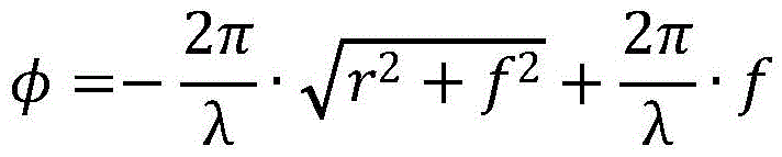
wherein, λ is the wavelength of light wave, r is the distance from each nano-pillar structure to the center of the substrate, and f is the focal length of the lens. The wavelength lambda is any wavelength in a target waveband of the superlens; in an example, the present embodiment is described by taking a superlens with a target wavelength band of 400-700nm as an example, and the wavelength λ is an arbitrary wavelength within 400nm or more and 700nm or less.
The super lens focal length f is selected according to the fingerprint imaging requirement of the intelligent display device, the distance D between a display device panel and the super lens or the super lens array, the distance D between the super lens or the super lens array and the optical sensing unit photosurface and the super lens focal length f satisfy the imaging relation:

the distance D between the display panel and the super lens or the super lens array and the distance D between the super lens or the super lens array and the light sensing surface of the optical sensing unit are selected according to the actual requirement of the display device, and optionally, D is greater than or equal to 5mm and less than or equal to 15 mm; d is greater than or equal to 1mm and less than or equal to 5 mm.
The imaging unit is composed of a single superlens, or a superlens array including a plurality of superlenses. The super lens array is a square, rectangular or regular hexagon array consisting of a plurality of super lenses in the same plane; the periods of the superlens arrays at different positions are the same; the shape, size, material, optical phase of the mirror surface, focal length and film coating system of the super lens at different positions are all kept consistent. The size of the super lens array can be selected according to the requirements of the finger print sensor under the screen; the period of the superlens array is larger than the size of the superlens; the center position of the super lens array is coaxially arranged with the photosensitive surface of the optical sensing unit. In the present embodiment, the superlens is a circular lens with a diameter of 0.975 mm; the super lens is in the range of 400-700nm band, the optical phase of the mirror surface meets the phase distribution of the non-chromatic aberration focusing lens, the focal length of the super lens is 2.73mm, and the micro-nano structure schematic diagram of the super lens is shown in FIG. 4; one side of the super surface structure unit of the super lens is plated with an anti-reflection film 212 with a wavelength band of 400-700nm, and the other side of the super lens is plated with an anti-reflection film with a target wavelength band matched with the substrate material, and the anti-reflection film system and the thickness schematic diagram are shown in fig. 5. The optical imaging unit consists of 3 × 3 square super lens arrays consisting of 9 identical super lenses, and the schematic diagram of the super lens arrays is shown in fig. 6; wherein the center distance between the adjacent superlenses is 1.3 mm. It can be understood that, in the under-screen fingerprint sensor, the size and shape of the superlens array, the size of the superlens, the shape of the superlens, the focal length of the superlens, the number of the superlenses, the arrangement mode and the arrangement period of the superlenses can be other choices for satisfying the purpose of under-screen fingerprint imaging.
The optical imaging unit is erected at the windowing position of the light guide layer. The light guide layer is transparent in a target waveband; the shape of the light guide layer is any shape which meets the requirement of fingerprint detection light collection, and the shape includes but is not limited to a circle, a rectangle, a regular polygon and the like; the size of the cross section of the light guide layer is larger than that of the optical imaging unit, and the light guide layer can be any size meeting the requirements of display equipment; the light guide layer is transparent in a target waveband, the material of the light guide layer can be any choice meeting the requirement, and optionally, the material of the light guide layer can be silicon oxide; the thickness of the light guide layer determines the vertical distance D between the optical imaging unit and the photosensitive surface of the optical sensing unit, and the thickness of the light guide layer can be any size meeting the imaging condition of the fingerprint under the screen. The light guide layer is provided with a window at one side close to the display equipment panel; the windowing part is in any shape meeting the erection requirement of the imaging unit, and the windowing part can be selected from circular shapes, square shapes, regular polygons and the like; the windowing size is larger than the imaging unit size and can be any size that meets the assumed requirements of the imaging unit. The light guide layer is positioned below the display panel; the distance d between the light guide layer and the display panel meets the imaging condition; the center position of the window of the light guide layer deviates from the fingerprint identification area of the display panel and is symmetrically arranged with the fingerprint identification light source of the display device so as to receive the detection light reflected by the fingerprint. In the present embodiment, a circular light guide layer with a diameter of 3cm (unit: cm) and a thickness of 5.05mm is exemplified as an example; the light guide layer is made of silicon oxide; a square window with the side length of 3.9mm is arranged at the center of the upper surface of the light guide layer; the windowing depth is 0.35 mm; the window and the photosensitive surface of the optical sensing unit are coaxially arranged; the distance between the light guide layer and the OLED display panel is 5.93 mm. It will be appreciated that the shape, size, and material of the light guiding layer of the underscreen fingerprint sensor of the present embodiment may be other options that meet the requirements of the superlens array configuration and the underscreen fingerprint imaging.
In the fingerprint sensor, detection light reflected by a fingerprint is collected and imaged on a photosensitive surface of the optical sensing unit through the optical imaging unit, and the photosensitive surface senses optical signals of a target waveband and converts the optical signals into electric signals to output a fingerprint image for post-processing. The type of the optical sensing unit is selected according to a target waveband of the finger print sensor under the screen; the light sensing surface of the optical sensing unit faces the light guide layer; the light sensing surface is close to one side of the light guide layer, which is far away from the display panel, and is coaxially arranged with the optical imaging unit; the shape of the photosensitive surface is any choice meeting the imaging of the finger print under the screen, and optionally, the shape of the photosensitive surface comprises a circle, a square and a polygon; the size of the photosensitive surface is any size larger than the imaging range of the fingerprint. For example, the present embodiment is described by taking an optical sensing unit array as an example; the optical sensing unit array is a 3 x 3 square array consisting of 9 optical sensing units with the same parameters; each sensing unit in the optical sensing unit array corresponds to each super lens in the super lens array; in the optical sensing unit array, the light sensing surface of each optical sensing unit is coaxially arranged with the superlens at the corresponding position in the superlens array; the working wavelength of the optical sensing unit comprises a 400-700nm band; the optical sensing unit is provided with a rectangular optical sensing surface; the length of the photosensitive surface is 2.842mm, and the width is 2.121 mm. The output of the underscreen fingerprint sensor is shown schematically in fig. 7A. It can be understood that, in the embodiment, in the optical sensing unit array, the parameters such as the number, arrangement, shape and size of the sensing units may be other parameters meeting the requirements of fingerprint detection light imaging in the 400-700nm wavelength range.
Example two
The embodiment provides an under-screen fingerprint sensor suitable for an intelligent display device carrying an LCD screen, and the structure of the embodiment refers to FIG. 1B. As shown in fig. 1B, the underscreen fingerprint sensor includes: light guide layer 1, imaging unit 2, optical sensing unit 3 and base 4. Wherein, the light guide layer 1 is positioned on the optical sensing unit 3; the light guide layer 1 is provided with a window 5 corresponding to the fingerprint detection direction; the imaging unit 2 is erected at the position of the window 5 of the light guide layer 1 by a superlens. Fingerprint sensor arranges display device panel 7 below in under the screen, and fingerprint detection light is provided by extra near-infrared light source, and on fingerprint reflection detected the light back by the imaging unit cell-phone and formation of image to the photosurface of optical sensing unit, the photosurface absorbed fingerprint detection light and converted into fingerprint image electricity signal output. This embodiment will be described by taking a narrow-band fingerprint detection light source with a center wavelength of 940nm as an example.
The super lens comprises a substrate 21 and an array formed by super surface structure units 22 arranged on the surface of the substrate, and the array is shown in fig. 2A; the target operating wavelength of the superlens or the superlens array is 940 nm; the superlens substrate 21 can transmit light with a wavelength of 940 nm; the substrate material is a near-infrared band transparent material; optionally, the substrate material comprises silicon oxide. For example, the present embodiment is described with silicon oxide as a base material; it will be appreciated that the substrate material may be other choices that meet the need for transparency in the target wavelength range. In this embodiment, the thickness of the superlens substrate 21 may be selected as required; optionally, the thickness of the substrate 21 is greater than or equal to 0.1mm and less than or equal to 0.3 mm. By way of example, the present embodiment is described with a substrate of 0.3mm thickness as an example; it will be appreciated that the substrate thickness may be other choices that meet the transparency requirements in the target wavelength band.
In this embodiment, the super-lens substrate 21 has super-surface structure units 22 arranged periodically on the surface; the unit periods of the periodic array at different positions are the same; the units of the super-surface structure are arranged in a regular hexagon; the center of each super-surface structure unit is provided with a nano-structure, and the array is illustrated in fig. 2B. It will be appreciated that the arrangement of the units of the super-surface structure may be other choices to meet the requirements.
The nano structure is a nano column structure; optionally, the columnar structure includes one or more of a positive nanorod structure, a negative nanorod structure, a hollow nanorod structure, a negative hollow nanorod structure, and a topological nanorod structure. For example, the present embodiment is described by taking a positive nanorod as an example; the nano-structure material is amorphous silicon and is transparent at 940 nm. The cross-sectional shape of the nano-pillar structure can be one or a combination of circular, elliptical, quadrilateral, pentagonal, hexagonal and topological shapes. In an example, the present embodiment is illustrated by taking a positive nanorod with a circular cross section as an example, and referring to fig. 3A. It will be appreciated that the nanostructure material and shape may be selected to be otherwise transparent in the operating band of the superlens.
The geometrical size of the nano-pillar array structure comprises the height of the nano-pillars, the diameter of the cross section and the distance between the nano-pillars, and is selected according to the requirement of fingerprint detection. In the embodiment, the heights of the nano-pillar structures at different positions are all 500 nm; the distance between the centers of the adjacent nano-pillar structures is 404.15 nm; the diameter and the side length of the cross section of the nano column and/or the minimum distance between two adjacent nano column structures are more than or equal to 80nm and less than or equal to 330 nm; the maximum aspect ratio of the nano-pillar structure, i.e. the ratio of the height of the nano-pillar structure to the minimum diameter of the nano-pillar structure in the superlens, is less than or equal to 20. The relationship between the optical phase of the nanopillar at the wavelength of 940nm and the nanopillar diameter is seen in fig. 3D; the relationship between the nanopillar structure transmittance and the nanopillar diameter at a wavelength of 940nm is shown in fig. 3E. It will be appreciated that the geometry and dimensions of the nano-pillar structures may be other choices that meet the detection requirements and processing conditions.
The super lens is a circular super lens with the diameter of 0.712mm and is arranged at the windowing position of the light guide layer; the phase of the mirror surface light of the super lens at the 940nm wave band meets the phase distribution of the positive lens without chromatic aberration:
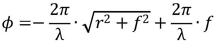
wherein, λ is the wavelength of light wave, r is the distance from each nano-pillar structure to the center of the substrate, and f is the focal length of the lens.
The light guide layer is transparent in a target waveband; the shape of the light guide layer is any shape which meets the requirement of fingerprint detection light collection, and the shape includes but is not limited to a circle, a rectangle, a regular polygon and the like; the size of the cross section of the light guide layer is larger than that of the optical imaging unit, and the light guide layer can be any size meeting the requirements of display equipment; the thickness of the light guide layer determines the vertical distance D between the photosensitive surfaces of the optical imaging unit and the optical sensing unit; the window is in any shape meeting the erection requirement of the imaging unit; the windowing size is larger than the size of the superlens; the light guide layer is positioned below the display panel; the distance d between the light guide layer and the display panel meets the imaging condition. In the present embodiment, a circular light guide layer made of silicon oxide having a diameter of 3cm and a thickness of 2.19mm is exemplified; a circular window with the diameter of 0.72mm is arranged at the center of the upper surface of the light guide layer; the windowing depth is 0.35 mm; the window and the photosensitive surface of the optical sensing unit are coaxially arranged; the distance between the light guide layer and the LCD display panel is 7.17 mm. It will be appreciated that the shape, size, and material of the light guiding layer of the underscreen fingerprint sensor of the present embodiment may be other options that meet the requirements of superlens construction and underscreen fingerprint imaging.
In the fingerprint sensor, detection light reflected by a fingerprint is collected and imaged by the optical imaging unit and forms an image of a photosensitive surface of the optical sensing unit, and the optical photosensitive surface senses optical signals of a target waveband and converts the optical signals into electric signals to output a fingerprint image for post-processing. The present embodiment takes an optical sensing unit with a wavelength of 940nm as an example for explanation; the optical sensing unit is provided with a rectangular optical sensing surface; the length of the photosensitive surface is 2.842mm, and the width of the photosensitive surface is 2.121 mm; the output of the underscreen fingerprint sensor is shown schematically in fig. 7B. It is understood that, in the present embodiment, the shape, size, and other parameters of the photosensitive surface may be other choices for meeting the requirement of collecting the fingerprint detection light.
The utility model provides a fingerprint sensor and display device under screen based on super lens compares in traditional fingerprint sensor and display device based on optical lens, and the effectual integrated level that improves the sensor of introduction of super lens, greatly reduced under the screen fingerprint sensor to intelligent display device's dimensional requirement, can further reduce display device's overall dimension.
The above embodiments are only used to illustrate the technical solution of the present invention, and not to limit it; although the present invention has been described in detail with reference to the foregoing embodiments, it will be understood by those of ordinary skill in the art that: the technical solutions described in the foregoing embodiments may still be modified, or some technical features may be equivalently replaced; such modifications and substitutions do not depart from the spirit and scope of the present invention in its corresponding aspects.
Claims (15)
1. An underscreen fingerprint sensor based on a superlens, comprising
A base;
the optical sensing unit is arranged on the base and comprises a photosensitive unit array;
the light guide layer is positioned above the optical sensing unit, and a window is arranged on the light guide layer corresponding to the fingerprint detection direction;
and the imaging unit comprises a super lens or a super lens array, and the super lens or the super lens array is erected at the windowing position of the light guide layer.
2. The underscreen fingerprint sensor of claim 1, wherein the superlens comprises: the substrate and locate super surface structure unit on substrate surface, super surface structure unit is array arrangement.
3. The underscreen fingerprint sensor of claim 2, wherein the units of the super-surface structure are periodically arranged in an array, the periods of the units of the super-surface structure at different positions in the array being the same.
4. The underscreen fingerprint sensor according to claim 2, wherein the super-surface structure units are regular hexagons or regular tetragons, and the nano-structures are respectively arranged at the central positions of the super-surface structure units.
5. The underscreen fingerprint sensor of claim 4, wherein the nanostructures are nanopillar structures.
6. The underscreen fingerprint sensor of claim 5, wherein the nano-pillar structures comprise one or more of positive nano-pillar structures, negative nano-pillar structures, hollow nano-pillar structures, and topological nano-pillar structures.
7. The underscreen fingerprint sensor of claim 6, wherein the cross-sectional shape of the nano-pillar structure is one or a combination of two or more of a circle, an ellipse, a polygon and a topological shape.
8. The underscreen fingerprint sensor of claim 5, wherein the height of the nano-pillar structures is greater than or equal to 300nm and less than or equal to 2000nm, the diameter, the side length and/or the minimum distance between two adjacent nano-pillar structures is greater than or equal to 80nm, and the maximum aspect ratio of the nano-pillar structures, that is, the ratio of the height of the nano-pillar structures to the minimum diameter of the nano-pillar structures in the superlens, is less than or equal to 20.
9. The underscreen fingerprint sensor according to claim 2, wherein the substrate is a transparent substrate with a target wavelength band, the thickness of the transparent substrate is ≧ 0.1mm and ≦ 0.3mm, and the wavelength range of the target wavelength band is 400-700nm or 900-1200 nm.
10. The underscreen fingerprint sensor of claim 2, wherein one side of the super surface structure unit of the super lens is plated with an antireflection film of a target waveband, and the other side of the super lens is plated with an antireflection film of a target waveband matched with a substrate material.
11. The underscreen fingerprint sensor of claim 2, wherein the superlens is circular or square, the circular superlens having a diameter size in the range of 0.5-3 mm;
the side length size range of the square super lens is 0.5-3 mm;
the superlens has an achromatic positive lens phase distribution in a target wavelength band.
12. The underscreen fingerprint sensor of claim 2, wherein the nanostructure side of the superlens faces the light-sensing surface of the optical sensing unit;
the super lens or the super lens array and the photosensitive unit array are coaxially arranged;
the distance between the super lens or the super lens array and the photosensitive unit array is 1-10 mm;
the focal length range of the superlens is 1-10 mm;
and the distance between the photosensitive surface of the optical sensing unit, the super lens or the super lens array and the display equipment panel meets the imaging condition.
13. The underscreen fingerprint sensor of claim 1, wherein the underscreen fingerprint sensor is suitable for a display device carrying an OLED screen or a display device carrying an LCD screen.
14. The underscreen fingerprint sensor of claim 13, wherein when used in a display device carrying an OLED screen, the superlens or superlens array of the underscreen fingerprint sensor has a target wavelength range of 400-700 nm; when used in a display device carrying an LCD screen, the target wavelength range of the superlens or superlens array of the underscreen fingerprint sensor is 900-1200 nm.
15. A display device comprising the superlens-based underscreen fingerprint sensor of any one of claims 1-14 disposed beneath a display panel of the display device.
Priority Applications (1)
| Application Number | Priority Date | Filing Date | Title |
|---|---|---|---|
| CN202022008894.2U CN213092332U (en) | 2020-09-14 | 2020-09-14 | Fingerprint sensor and display device under screen based on super lens |
Applications Claiming Priority (1)
| Application Number | Priority Date | Filing Date | Title |
|---|---|---|---|
| CN202022008894.2U CN213092332U (en) | 2020-09-14 | 2020-09-14 | Fingerprint sensor and display device under screen based on super lens |
Publications (1)
| Publication Number | Publication Date |
|---|---|
| CN213092332U true CN213092332U (en) | 2021-04-30 |
Family
ID=75635281
Family Applications (1)
| Application Number | Title | Priority Date | Filing Date |
|---|---|---|---|
| CN202022008894.2U Active CN213092332U (en) | 2020-09-14 | 2020-09-14 | Fingerprint sensor and display device under screen based on super lens |
Country Status (1)
| Country | Link |
|---|---|
| CN (1) | CN213092332U (en) |
Cited By (11)
| Publication number | Priority date | Publication date | Assignee | Title |
|---|---|---|---|---|
| CN113345925A (en) * | 2021-05-31 | 2021-09-03 | 北京京东方技术开发有限公司 | Pixel unit, image sensor and spectrometer |
| WO2021233416A1 (en) * | 2020-05-22 | 2021-11-25 | 深圳迈塔兰斯科技有限公司 | Hybrid optical system having superlens and refraction and/or reflection lens |
| CN113807312A (en) * | 2021-09-30 | 2021-12-17 | 深圳迈塔兰斯科技有限公司 | Super surface and have its fingerprint identification device |
| US11927769B2 (en) | 2022-03-31 | 2024-03-12 | Metalenz, Inc. | Polarization sorting metasurface microlens array device |
| US11978752B2 (en) | 2019-07-26 | 2024-05-07 | Metalenz, Inc. | Aperture-metasurface and hybrid refractive-metasurface imaging systems |
| US11988844B2 (en) | 2017-08-31 | 2024-05-21 | Metalenz, Inc. | Transmissive metasurface lens integration |
| WO2024152972A1 (en) * | 2023-01-18 | 2024-07-25 | Chiun Mai Communication Systems, Inc. | Metalens array and display device having same |
| US12140778B2 (en) | 2018-07-02 | 2024-11-12 | Metalenz, Inc. | Metasurfaces for laser speckle reduction |
| US12416752B2 (en) | 2018-01-24 | 2025-09-16 | President And Fellows Of Harvard College | Polarization state generation with a metasurface |
| US12460919B2 (en) | 2019-10-31 | 2025-11-04 | President And Fellows Of Harvard College | Compact metalens depth sensors |
| US12548980B2 (en) | 2022-05-25 | 2026-02-10 | Metalenz, Inc. | Single element dot pattern projector |
-
2020
- 2020-09-14 CN CN202022008894.2U patent/CN213092332U/en active Active
Cited By (17)
| Publication number | Priority date | Publication date | Assignee | Title |
|---|---|---|---|---|
| US12411348B2 (en) | 2017-08-31 | 2025-09-09 | Metalenz, Inc. | Transmissive metasurface lens integration |
| US11988844B2 (en) | 2017-08-31 | 2024-05-21 | Metalenz, Inc. | Transmissive metasurface lens integration |
| US12416752B2 (en) | 2018-01-24 | 2025-09-16 | President And Fellows Of Harvard College | Polarization state generation with a metasurface |
| US12140778B2 (en) | 2018-07-02 | 2024-11-12 | Metalenz, Inc. | Metasurfaces for laser speckle reduction |
| US12389700B2 (en) | 2019-07-26 | 2025-08-12 | Metalenz, Inc. | Aperture-metasurface and hybrid refractive-metasurface imaging systems |
| US11978752B2 (en) | 2019-07-26 | 2024-05-07 | Metalenz, Inc. | Aperture-metasurface and hybrid refractive-metasurface imaging systems |
| US12460919B2 (en) | 2019-10-31 | 2025-11-04 | President And Fellows Of Harvard College | Compact metalens depth sensors |
| WO2021233416A1 (en) * | 2020-05-22 | 2021-11-25 | 深圳迈塔兰斯科技有限公司 | Hybrid optical system having superlens and refraction and/or reflection lens |
| CN113345925A (en) * | 2021-05-31 | 2021-09-03 | 北京京东方技术开发有限公司 | Pixel unit, image sensor and spectrometer |
| CN113345925B (en) * | 2021-05-31 | 2024-04-12 | 北京京东方技术开发有限公司 | Pixel unit, image sensor and spectrometer |
| WO2023050884A1 (en) * | 2021-09-30 | 2023-04-06 | 深圳迈塔兰斯科技有限公司 | Metasurface and fingerprint recognition device having same |
| CN113807312B (en) * | 2021-09-30 | 2024-10-18 | 深圳迈塔兰斯科技有限公司 | Super surface and fingerprint identification device with same |
| CN113807312A (en) * | 2021-09-30 | 2021-12-17 | 深圳迈塔兰斯科技有限公司 | Super surface and have its fingerprint identification device |
| US11927769B2 (en) | 2022-03-31 | 2024-03-12 | Metalenz, Inc. | Polarization sorting metasurface microlens array device |
| US12276807B2 (en) | 2022-03-31 | 2025-04-15 | Metalenz, Inc. | Polarization sorting metasurface microlens array device |
| US12548980B2 (en) | 2022-05-25 | 2026-02-10 | Metalenz, Inc. | Single element dot pattern projector |
| WO2024152972A1 (en) * | 2023-01-18 | 2024-07-25 | Chiun Mai Communication Systems, Inc. | Metalens array and display device having same |
Similar Documents
| Publication | Publication Date | Title |
|---|---|---|
| CN213092332U (en) | Fingerprint sensor and display device under screen based on super lens | |
| CN213902664U (en) | Thermopile infrared sensor | |
| CN1227419A (en) | Optoelectronic device, optoelectronic module and method for setting up optoelectronic system | |
| KR102610600B1 (en) | Fingerprint recognition method, fingerprint recognition device and electronic device | |
| WO2023093118A1 (en) | Telecentric lens and laser radar transmitting and receiving system comprising same | |
| US20160043259A1 (en) | Non-Imaging Light Concentrator | |
| CN101770072B (en) | A compound field of view sensor imaging system | |
| JPS59112202U (en) | solar energy concentrator | |
| CN101923209B (en) | Light harvesting device | |
| CN110928017A (en) | Display panel | |
| JP2000101124A (en) | Concentrating photovoltaic module, method of manufacturing the same, and concentrating photovoltaic system | |
| CN109685034B (en) | Fingerprint identification module and display device | |
| WO2022032843A1 (en) | Micro spectral chip based on units of different shapes | |
| CN106057957B (en) | Avalanche photodide with periodic nano-structure | |
| TW201201389A (en) | Electromagnetic wave gathering device and solar cell module with the same | |
| CN110781848B (en) | Screen fingerprint identification device and electronic equipment | |
| CN218240537U (en) | Two-piece optical lens, fingerprint identification device comprising two-piece optical lens and electronic equipment comprising two-piece optical lens | |
| JP2002026364A (en) | Concentrating solar power generator | |
| JPH1131837A (en) | Concentrating solar power generation device and module using the same | |
| CN120224857A (en) | Silicon wafer and preparation method thereof, solar cell and preparation method thereof | |
| JP2005340583A (en) | Photosensitive surface structure of photovoltaic generator | |
| JP2735154B2 (en) | Concentrating solar cell module | |
| CN212484388U (en) | OCR gathers and indicates fingerprint collection integration equipment more | |
| JP2014134790A (en) | Convergence device and convergence module | |
| CN116699748B (en) | Super-surface light-splitting module, image sensor, lens module and electronic equipment |
Legal Events
| Date | Code | Title | Description |
|---|---|---|---|
| GR01 | Patent grant | ||
| GR01 | Patent grant | ||
| CP02 | Change in the address of a patent holder | ||
| CP02 | Change in the address of a patent holder |
Address after: 518000 floor 6, building 8, qiugu, Meisheng Huigu science and Technology Park, No. 83, Dabao Road, district 33, Shanghe community, Xin'an street, Bao'an District, Shenzhen, Guangdong Province Patentee after: Shenzhen maitalans Technology Co.,Ltd. Address before: 518101 building 619, Hanyu Bioengineering Co., Ltd., Liyuan Road, Tangwei community, Fuhai street, Bao'an District, Shenzhen, Guangdong Patentee before: Shenzhen maitalans Technology Co.,Ltd. |