CN212660328U - Microphone assembly and assembled PCB - Google Patents
Microphone assembly and assembled PCB Download PDFInfo
- Publication number
- CN212660328U CN212660328U CN202021960819.XU CN202021960819U CN212660328U CN 212660328 U CN212660328 U CN 212660328U CN 202021960819 U CN202021960819 U CN 202021960819U CN 212660328 U CN212660328 U CN 212660328U
- Authority
- CN
- China
- Prior art keywords
- edge
- edges
- solder
- coupled
- substrate
- Prior art date
- Legal status (The legal status is an assumption and is not a legal conclusion. Google has not performed a legal analysis and makes no representation as to the accuracy of the status listed.)
- Active
Links
- 239000000758 substrate Substances 0.000 claims abstract description 56
- 229910000679 solder Inorganic materials 0.000 claims description 80
- 230000001681 protective effect Effects 0.000 claims description 21
- 239000000463 material Substances 0.000 claims description 5
- 238000002844 melting Methods 0.000 claims description 5
- 230000008018 melting Effects 0.000 claims description 5
- 238000000034 method Methods 0.000 description 29
- 230000000712 assembly Effects 0.000 description 27
- 238000000429 assembly Methods 0.000 description 27
- 230000008569 process Effects 0.000 description 12
- 230000008878 coupling Effects 0.000 description 9
- 238000010168 coupling process Methods 0.000 description 9
- 238000005859 coupling reaction Methods 0.000 description 9
- 239000000853 adhesive Substances 0.000 description 7
- 230000001070 adhesive effect Effects 0.000 description 7
- 239000003822 epoxy resin Substances 0.000 description 7
- 238000004519 manufacturing process Methods 0.000 description 7
- 229920000647 polyepoxide Polymers 0.000 description 7
- XUIMIQQOPSSXEZ-UHFFFAOYSA-N Silicon Chemical compound [Si] XUIMIQQOPSSXEZ-UHFFFAOYSA-N 0.000 description 5
- VYPSYNLAJGMNEJ-UHFFFAOYSA-N Silicium dioxide Chemical compound O=[Si]=O VYPSYNLAJGMNEJ-UHFFFAOYSA-N 0.000 description 4
- 229920005989 resin Polymers 0.000 description 4
- 239000011347 resin Substances 0.000 description 4
- 229910052710 silicon Inorganic materials 0.000 description 4
- 239000010703 silicon Substances 0.000 description 4
- 239000004593 Epoxy Substances 0.000 description 3
- 230000008859 change Effects 0.000 description 3
- 238000004891 communication Methods 0.000 description 3
- 239000004020 conductor Substances 0.000 description 3
- 238000010438 heat treatment Methods 0.000 description 3
- XEEYBQQBJWHFJM-UHFFFAOYSA-N Iron Chemical compound [Fe] XEEYBQQBJWHFJM-UHFFFAOYSA-N 0.000 description 2
- PXHVJJICTQNCMI-UHFFFAOYSA-N Nickel Chemical compound [Ni] PXHVJJICTQNCMI-UHFFFAOYSA-N 0.000 description 2
- BQCADISMDOOEFD-UHFFFAOYSA-N Silver Chemical compound [Ag] BQCADISMDOOEFD-UHFFFAOYSA-N 0.000 description 2
- 229910000831 Steel Inorganic materials 0.000 description 2
- RTAQQCXQSZGOHL-UHFFFAOYSA-N Titanium Chemical compound [Ti] RTAQQCXQSZGOHL-UHFFFAOYSA-N 0.000 description 2
- 229910052782 aluminium Inorganic materials 0.000 description 2
- XAGFODPZIPBFFR-UHFFFAOYSA-N aluminium Chemical compound [Al] XAGFODPZIPBFFR-UHFFFAOYSA-N 0.000 description 2
- 238000010276 construction Methods 0.000 description 2
- 230000004907 flux Effects 0.000 description 2
- 230000007246 mechanism Effects 0.000 description 2
- 239000007769 metal material Substances 0.000 description 2
- 239000000565 sealant Substances 0.000 description 2
- 229910052709 silver Inorganic materials 0.000 description 2
- 239000004332 silver Substances 0.000 description 2
- 239000010959 steel Substances 0.000 description 2
- 239000010936 titanium Substances 0.000 description 2
- 229910052719 titanium Inorganic materials 0.000 description 2
- GSJBKPNSLRKRNR-UHFFFAOYSA-N $l^{2}-stannanylidenetin Chemical group [Sn].[Sn] GSJBKPNSLRKRNR-UHFFFAOYSA-N 0.000 description 1
- RZVAJINKPMORJF-UHFFFAOYSA-N Acetaminophen Chemical compound CC(=O)NC1=CC=C(O)C=C1 RZVAJINKPMORJF-UHFFFAOYSA-N 0.000 description 1
- RYGMFSIKBFXOCR-UHFFFAOYSA-N Copper Chemical compound [Cu] RYGMFSIKBFXOCR-UHFFFAOYSA-N 0.000 description 1
- 239000004642 Polyimide Substances 0.000 description 1
- 238000009825 accumulation Methods 0.000 description 1
- PNEYBMLMFCGWSK-UHFFFAOYSA-N aluminium oxide Inorganic materials [O-2].[O-2].[O-2].[Al+3].[Al+3] PNEYBMLMFCGWSK-UHFFFAOYSA-N 0.000 description 1
- 239000000919 ceramic Substances 0.000 description 1
- 229910010293 ceramic material Inorganic materials 0.000 description 1
- 238000011109 contamination Methods 0.000 description 1
- 229910052802 copper Inorganic materials 0.000 description 1
- 239000010949 copper Substances 0.000 description 1
- 239000012530 fluid Substances 0.000 description 1
- 239000011521 glass Substances 0.000 description 1
- PCHJSUWPFVWCPO-UHFFFAOYSA-N gold Chemical compound [Au] PCHJSUWPFVWCPO-UHFFFAOYSA-N 0.000 description 1
- 229910052737 gold Inorganic materials 0.000 description 1
- 239000010931 gold Substances 0.000 description 1
- 230000000977 initiatory effect Effects 0.000 description 1
- 229910052742 iron Inorganic materials 0.000 description 1
- KJLLKLRVCJAFRY-UHFFFAOYSA-N mebutizide Chemical compound ClC1=C(S(N)(=O)=O)C=C2S(=O)(=O)NC(C(C)C(C)CC)NC2=C1 KJLLKLRVCJAFRY-UHFFFAOYSA-N 0.000 description 1
- 229910052751 metal Inorganic materials 0.000 description 1
- 239000002184 metal Substances 0.000 description 1
- 229910001092 metal group alloy Inorganic materials 0.000 description 1
- 238000010295 mobile communication Methods 0.000 description 1
- 238000012986 modification Methods 0.000 description 1
- 230000004048 modification Effects 0.000 description 1
- 239000003607 modifier Substances 0.000 description 1
- 229910052759 nickel Inorganic materials 0.000 description 1
- 230000003287 optical effect Effects 0.000 description 1
- 238000004806 packaging method and process Methods 0.000 description 1
- 230000002093 peripheral effect Effects 0.000 description 1
- 229920001721 polyimide Polymers 0.000 description 1
- 238000003825 pressing Methods 0.000 description 1
- 239000005297 pyrex Substances 0.000 description 1
- 239000010453 quartz Substances 0.000 description 1
- 239000004065 semiconductor Substances 0.000 description 1
- 238000000926 separation method Methods 0.000 description 1
- 239000000377 silicon dioxide Substances 0.000 description 1
- 229910052814 silicon oxide Inorganic materials 0.000 description 1
- 238000005476 soldering Methods 0.000 description 1
- 229920001169 thermoplastic Polymers 0.000 description 1
- 239000012815 thermoplastic material Substances 0.000 description 1
- 239000004416 thermosoftening plastic Substances 0.000 description 1
- 238000009736 wetting Methods 0.000 description 1
Images


Classifications
-
- H—ELECTRICITY
- H04—ELECTRIC COMMUNICATION TECHNIQUE
- H04R—LOUDSPEAKERS, MICROPHONES, GRAMOPHONE PICK-UPS OR LIKE ACOUSTIC ELECTROMECHANICAL TRANSDUCERS; DEAF-AID SETS; PUBLIC ADDRESS SYSTEMS
- H04R31/00—Apparatus or processes specially adapted for the manufacture of transducers or diaphragms therefor
- H04R31/006—Interconnection of transducer parts
-
- H—ELECTRICITY
- H04—ELECTRIC COMMUNICATION TECHNIQUE
- H04R—LOUDSPEAKERS, MICROPHONES, GRAMOPHONE PICK-UPS OR LIKE ACOUSTIC ELECTROMECHANICAL TRANSDUCERS; DEAF-AID SETS; PUBLIC ADDRESS SYSTEMS
- H04R19/00—Electrostatic transducers
- H04R19/005—Electrostatic transducers using semiconductor materials
-
- B—PERFORMING OPERATIONS; TRANSPORTING
- B81—MICROSTRUCTURAL TECHNOLOGY
- B81B—MICROSTRUCTURAL DEVICES OR SYSTEMS, e.g. MICROMECHANICAL DEVICES
- B81B7/00—Microstructural systems; Auxiliary parts of microstructural devices or systems
- B81B7/0032—Packages or encapsulation
- B81B7/0045—Packages or encapsulation for reducing stress inside of the package structure
- B81B7/0051—Packages or encapsulation for reducing stress inside of the package structure between the package lid and the substrate
-
- B—PERFORMING OPERATIONS; TRANSPORTING
- B81—MICROSTRUCTURAL TECHNOLOGY
- B81B—MICROSTRUCTURAL DEVICES OR SYSTEMS, e.g. MICROMECHANICAL DEVICES
- B81B7/00—Microstructural systems; Auxiliary parts of microstructural devices or systems
- B81B7/008—MEMS characterised by an electronic circuit specially adapted for controlling or driving the same
-
- B—PERFORMING OPERATIONS; TRANSPORTING
- B81—MICROSTRUCTURAL TECHNOLOGY
- B81C—PROCESSES OR APPARATUS SPECIALLY ADAPTED FOR THE MANUFACTURE OR TREATMENT OF MICROSTRUCTURAL DEVICES OR SYSTEMS
- B81C1/00—Manufacture or treatment of devices or systems in or on a substrate
- B81C1/00015—Manufacture or treatment of devices or systems in or on a substrate for manufacturing microsystems
- B81C1/00261—Processes for packaging MEMS devices
- B81C1/00309—Processes for packaging MEMS devices suitable for fluid transfer from the MEMS out of the package or vice versa, e.g. transfer of liquid, gas, sound
-
- H—ELECTRICITY
- H04—ELECTRIC COMMUNICATION TECHNIQUE
- H04R—LOUDSPEAKERS, MICROPHONES, GRAMOPHONE PICK-UPS OR LIKE ACOUSTIC ELECTROMECHANICAL TRANSDUCERS; DEAF-AID SETS; PUBLIC ADDRESS SYSTEMS
- H04R1/00—Details of transducers, loudspeakers or microphones
- H04R1/02—Casings; Cabinets ; Supports therefor; Mountings therein
- H04R1/021—Casings; Cabinets ; Supports therefor; Mountings therein incorporating only one transducer
-
- H—ELECTRICITY
- H04—ELECTRIC COMMUNICATION TECHNIQUE
- H04R—LOUDSPEAKERS, MICROPHONES, GRAMOPHONE PICK-UPS OR LIKE ACOUSTIC ELECTROMECHANICAL TRANSDUCERS; DEAF-AID SETS; PUBLIC ADDRESS SYSTEMS
- H04R19/00—Electrostatic transducers
- H04R19/04—Microphones
-
- B—PERFORMING OPERATIONS; TRANSPORTING
- B23—MACHINE TOOLS; METAL-WORKING NOT OTHERWISE PROVIDED FOR
- B23K—SOLDERING OR UNSOLDERING; WELDING; CLADDING OR PLATING BY SOLDERING OR WELDING; CUTTING BY APPLYING HEAT LOCALLY, e.g. FLAME CUTTING; WORKING BY LASER BEAM
- B23K1/00—Soldering, e.g. brazing, or unsoldering
- B23K1/0008—Soldering, e.g. brazing, or unsoldering specially adapted for particular articles or work
-
- B—PERFORMING OPERATIONS; TRANSPORTING
- B81—MICROSTRUCTURAL TECHNOLOGY
- B81B—MICROSTRUCTURAL DEVICES OR SYSTEMS, e.g. MICROMECHANICAL DEVICES
- B81B2201/00—Specific applications of microelectromechanical systems
- B81B2201/02—Sensors
- B81B2201/0257—Microphones or microspeakers
-
- B—PERFORMING OPERATIONS; TRANSPORTING
- B81—MICROSTRUCTURAL TECHNOLOGY
- B81B—MICROSTRUCTURAL DEVICES OR SYSTEMS, e.g. MICROMECHANICAL DEVICES
- B81B2207/00—Microstructural systems or auxiliary parts thereof
- B81B2207/05—Arrays
- B81B2207/053—Arrays of movable structures
-
- B—PERFORMING OPERATIONS; TRANSPORTING
- B81—MICROSTRUCTURAL TECHNOLOGY
- B81C—PROCESSES OR APPARATUS SPECIALLY ADAPTED FOR THE MANUFACTURE OR TREATMENT OF MICROSTRUCTURAL DEVICES OR SYSTEMS
- B81C2203/00—Forming microstructural systems
- B81C2203/03—Bonding two components
- B81C2203/033—Thermal bonding
- B81C2203/035—Soldering
-
- H—ELECTRICITY
- H04—ELECTRIC COMMUNICATION TECHNIQUE
- H04R—LOUDSPEAKERS, MICROPHONES, GRAMOPHONE PICK-UPS OR LIKE ACOUSTIC ELECTROMECHANICAL TRANSDUCERS; DEAF-AID SETS; PUBLIC ADDRESS SYSTEMS
- H04R2201/00—Details of transducers, loudspeakers or microphones covered by H04R1/00 but not provided for in any of its subgroups
- H04R2201/003—Mems transducers or their use
Landscapes
- Engineering & Computer Science (AREA)
- Microelectronics & Electronic Packaging (AREA)
- Physics & Mathematics (AREA)
- Acoustics & Sound (AREA)
- Signal Processing (AREA)
- Manufacturing & Machinery (AREA)
- Computer Hardware Design (AREA)
- Micromachines (AREA)
Abstract
The utility model provides a microphone subassembly and PCB through the equipment. A microphone assembly includes a substrate defining a port, a MEMS transducer, a guard ring, and a cover. The MEMS transducer is coupled to the substrate such that the MEMS transducer is positioned over the port. A guard ring is coupled to the substrate and surrounds the MEMS transducer. The guard ring includes a plurality of edges that further include a first edge and an opposing second edge. A portion of the first edge and a portion of the second edge have a reduced thickness relative to an adjacent edge of the plurality of edges. The cap is coupled to the guard ring such that the substrate and the cap collectively define an internal cavity.
Description
Technical Field
The present disclosure relates to microelectromechanical systems (MEMS) devices, and more particularly to the fabrication of MEMS devices that include MEMS transducers.
Background
When building high performance, high density devices, such as mobile communication devices, portable music players, and other portable electronic devices, compact components are required. One solution to provide high quality, compact devices is to use micro-electromechanical systems (MEMS).
For example, microphone assemblies for many portable electronic devices include a MEMS acoustic transducer that converts acoustic energy into an electrical signal. MEMS acoustic transducers include a silicon chip mounted to a Printed Circuit Board (PCB) to form a microphone assembly. Despite the small silicon chips, existing manufacturing processes for these microphone assemblies are limited in the overall size of the silicon chip that can be accommodated within a given microphone package.
SUMMERY OF THE UTILITY MODEL
A first aspect of the present disclosure relates to a microphone assembly. The microphone assembly includes a substrate defining a port, a MEMS transducer, a guard ring, and a can. The MEMS transducer is coupled to the substrate such that the MEMS transducer is positioned over the port. The guard ring is coupled to the substrate and surrounds the MEMS transducer. The guard ring includes a plurality of edges that further include a first edge and an opposing second edge. A portion of the first edge and a portion of the second edge have a reduced thickness relative to an adjacent edge of the plurality of edges. The cap is coupled to the protective ring such that the substrate and the cap collectively (cooperatively) define an internal cavity.
A second aspect of the present disclosure relates to an assembled printed-circuit board (populated-circuit-board). The assembled printed circuit board includes a substrate and a plurality of guard rings. The plurality of guard rings are coupled to the substrate. Each of the plurality of guard rings includes a plurality of edges. A first edge of the plurality of edges and an opposing second edge of the plurality of edges have a reduced thickness relative to an adjacent edge of the plurality of edges.
A third aspect of the present disclosure is a method. The method includes providing a substrate defining a plurality of ports. The method also includes coupling a plurality of protection rings to the substrate such that each protection ring of the plurality of protection rings is positioned around a respective port of the plurality of ports. The method also includes coupling a plurality of MEMS transducers to the substrate, each MEMS transducer of the plurality of MEMS transducers positioned within a periphery of a respective guard ring of the plurality of guard rings and at least partially isolating a respective port of the plurality of ports. The method additionally includes applying solder along a single axis between each of the plurality of guard rings such that the solder is applied substantially equally to adjacent guard rings of the plurality of guard rings. The method also includes coupling a plurality of caps to the plurality of guard rings to form a plurality of coupled microphone assemblies, in which each cap of the plurality of caps is configured to enclose a respective MEMS transducer of the plurality of MEMS transducers. The method also includes separating each of the plurality of coupled microphone assemblies from the substrate to form a plurality of individual microphone assemblies.
The foregoing description is exemplary only and is not intended to be limiting in any way. In addition to the illustrative aspects, embodiments, and features described above, further aspects, embodiments, and features will become apparent by reference to the following drawings and detailed description.
Drawings
The foregoing and other features of the present disclosure will become more fully apparent from the following description and appended claims, taken in conjunction with the accompanying drawings. These drawings depict only several embodiments in accordance with the disclosure and are not therefore to be considered to be limiting of its scope. Various embodiments are described in more detail below in conjunction with the following figures.
Fig. 1 is a perspective view of a microphone assembly in accordance with an exemplary embodiment.
Fig. 2 is a top view of a microphone assembly on an assembled Printed Circuit Board (PCB) according to another exemplary embodiment.
Fig. 3 is a top view of a microphone assembly on an assembled PCB in accordance with another exemplary embodiment.
Fig. 4 is a perspective view of an assembled PCB and solder dispensing pin according to an exemplary embodiment.
Fig. 5 is a top view of a microphone assembly on an assembled PCB in accordance with another exemplary embodiment.
Fig. 6 is a top view of a microphone assembly on an assembled PCB in accordance with another exemplary embodiment.
Fig. 7 is a top view of a guard ring for the microphone assembly of fig. 5.
Fig. 8A is a top view of a guard ring for the microphone assembly of fig. 6.
FIG. 8B is a reproduction of FIG. 8A near the guard ring.
Fig. 9 is a flow chart of a method of manufacturing a coupled microphone assembly in accordance with an exemplary embodiment.
Fig. 10 is a top view of a PCB in accordance with an exemplary embodiment.
Fig. 11 is a top view of the PCB of fig. 10 including a plurality of guard rings in accordance with an exemplary embodiment.
FIG. 12 is a top view of the PCB of FIG. 10 including a plurality of MEMS transducers, according to an exemplary embodiment.
Fig. 13 is a top view of the PCB of fig. 10 after a single axis dispensing process in accordance with an exemplary embodiment.
Fig. 14 is a top view of the PCB of fig. 10 including a plurality of caps according to an exemplary embodiment.
Fig. 15 is a top view of a microphone assembly prior to a reflow process in accordance with an exemplary embodiment.
Fig. 16 is a top view of the microphone assembly of fig. 15 after a reflow process in accordance with an exemplary embodiment.
Fig. 17 is a top view of multiple microphone components on an assembled PCB according to an exemplary embodiment.
In the following detailed description, various embodiments are described with reference to the accompanying drawings. It will be appreciated by those skilled in the art that the drawings are schematic and simplified for clarity, and thus, the drawings show only those details that are essential to an understanding of the present disclosure, while omitting other details. Like reference numerals refer to like elements or components throughout. Therefore, the same elements or components do not have to be described in detail with respect to the respective drawings.
Detailed Description
Generally, disclosed herein is a microphone assembly produced using a single-wire axis solder dispensing process. The microphone assembly includes a MEMS acoustic transducer, an integrated circuit, a substrate, and a cover. The MEMS acoustic transducer may be a capacitive acoustic transducer comprising a fixed backplate and a movable diaphragm, the MEMS acoustic transducer being configured to convert acoustic energy incident on the diaphragm into an electrical signal. The MEMS acoustic transducer and the integrated circuit are coupled to a substrate. A conductive guard ring is also coupled to the substrate and surrounds the MEMS transducer and the integrated circuit. The cover is coupled to the guard ring by solder to at least partially acoustically and electrically isolate the MEMS acoustic transducer from the environment surrounding the microphone assembly. Conventionally, solder is applied to the guard ring by a dispensing pin in a picture frame pattern that extends along the entire guard ring (e.g., along the entire perimeter of the shroud and microphone assembly, along two axes, etc.). The solder dispensing process requires the needles to have a minimum gap from the MEMS transducer to avoid solder contamination (e.g., wetting) of the MEMS transducer surface and/or damage to the MEMS transducer due to contact by the needles. Such a gap requirement between the pin and the MEMS transducer limits the minimum size of microphone assembly packaging that can be achieved for the MEMS transducer.
Embodiments disclosed herein may reduce the overall size of a microphone assembly that can be achieved for a fixed size MEMS transducer without changing the size of the dispense needle. In particular, the microphone assembly disclosed herein is manufactured by dispensing solder along only two sides of the guard ring. In other words, the cover for the microphone assembly is coupled to the guard ring by solder that extends along the entire length of only two sides of the cover. A label of epoxy or another adhesive product is applied to the remaining side of the cover to maintain a hermetic seal between the MEMS transducer and the environment surrounding the microphone assembly.
During production, multiple microphone assemblies may be formed onto a single substrate to form an assembled PCB. As used herein, the term "coupled microphone assembly" refers to a microphone assembly that is connected to other microphone assemblies on an assembled PCB. The coupled microphone assemblies may be arranged in rows along the length of the PCB. The joined microphone assemblies may be aligned in the X-axis direction and the Y-axis direction, forming aligned rows and columns of joined microphone assemblies. In order to prepare the coupled microphone assembly for placement of the cover, solder is dispensed along a single axis between the guard rings of each of the coupled microphone assemblies. More specifically, solder is distributed along a single axis extending parallel to the longest edge (e.g., X-axis) of each of the guard rings.
Among other benefits, the single axis solder dispensing process allows for an increase in the overall size (e.g., footprint) of the silicon chip used within the microphone assembly without increasing the overall package size of the microphone assembly. The details of the general description provided above will be explained more fully with reference to fig. 1-17.
Fig. 1 illustrates an individual microphone assembly, shown as assembly 100, according to an illustrative embodiment. The assembly 100 includes a substrate 102; and a top (cap), lid or cap, shown as cap 104, coupled to the base plate. The cover 104 defines a continuous surface sized to surround and enclose all of the internal components of the assembly 100. In the embodiment of fig. 1, the cover 104 is made of a metallic material (e.g., aluminum, titanium, steel, etc.). The cover 104 is coupled to the substrate along a perimeter of the cover 104 using solder 106 (e.g., a reflowable conductive metal alloy, a lead-free solder, etc.) and an adhesive or sealant (e.g., an epoxy, etc.), shown as a label (tag) 108. Solder 106 electrically connects the cap 104 to a conductive material embedded within the substrate 102 or otherwise coupled to the substrate 102. Additionally, the solder 106 at least partially acoustically isolates the electronic components contained within the enclosure 104 from the environment surrounding the microphone assembly 100.
During production, multiple microphone assemblies may be formed on (e.g., assembled on) or otherwise coupled to a single substrate (e.g., substrate blank, etc.). The substrate may be a Printed Circuit Board (PCB) that includes printed circuit traces or pads to facilitate electrical connection between components of individual ones of the microphone assemblies. Fig. 2 illustrates a top view of a coupled microphone assembly shown as a full frame assembly 200, the full frame assembly 200 being produced using a two-axis solder dispensing process (e.g., a conventional solder dispensing process). The full frame assembly 200 is shown prior to separation from a larger assembled PCB (e.g., a PCB including a plurality of interconnected/coupled full frame assemblies 200). Fig. 3 shows a top view of the assembly 100 of fig. 1, the assembly 100 being made using a single axis dispensing process.
As shown in fig. 2, the full frame assembly 200 includes solder 206 that extends along the entire (e.g., all) perimeter of the cover 204. The thickness of the solder 206 is substantially uniform along the perimeter of the cap 204. In contrast, for the assembly 100 of fig. 1 and 3, the solder 106 extends along the entire length of only two sides of the cap 104. More specifically, the solder 106 extends along the entire length of the two longest sides 110 of the cover 104. In addition, solder 106 spreads around each of a plurality of corner regions 112 of cover 104 that connect longest side 110 with a short side 114, the short side 114 being arranged in a substantially perpendicular orientation with respect to longest side 110.
As shown in fig. 1 and 3, labels 108 are applied to respective short sides 114 of the cover 104 between the cover 104 and the substrate 102. More specifically, label 108 is applied to center location 116 along short side 114 at approximately half way (half-way) between corner regions 112 that define the ends of short side 114. The label 108 fills any gaps in the footprint of the solder 106 along the perimeter of the lid 104 to ensure an airtight seal along the entire perimeter of the lid 104. In some embodiments, the label 108 comprises a material having a melting point higher than the melting point of the solder 106. In some embodiments, the label 108 is and/or includes an epoxy. The epoxy resin may include a non-conductive epoxy resin (e.g., a resin-based alumina-filled epoxy resin, a resin-based silica-filled epoxy resin, etc.) and/or a conductive epoxy resin (e.g., a resin-based silver-filled epoxy resin, a resin-based nickel-filled epoxy resin, etc.). In other embodiments, the label 108 comprises another thermoplastic, polyimide, adhesive, or the like.
The size of the labels 108 and/or the number of labels 108 used on each short side 114 varies depending on the length of the short side 114, the amount of solder 106 used on the longest side 110, and the peak time and temperature to which the assembly 100 is exposed during the solder reflow operation. In the embodiment of fig. 1 and 3, the width of the assembly 100 is approximately 2.5mm, and after a reflow operation (as will be further described), the solder 106 covers approximately 1mm on either side of the label 108. The single label 108 in the embodiment of fig. 1 and 3 covers a distance of approximately 600 microns. Thus, in fig. 1 and 3, only a single label 108 is required to ensure an airtight seal between the cover 104 and the substrate 102. In other embodiments, the number of labels 108 and/or the amount of adhesive or sealant applied with each label 108 may be different.
Fig. 4 shows a top perspective view of the assembled PCB300 during a dispensing operation, wherein solder 106 is applied to the joined microphone assemblies 100 through the dispensing pin 302 (e.g., prior to placing the lid 104 over the respective assemblies 100). The flow rate of solder 106 through the dispensing needle 302 is approximately constant throughout the dispensing operation. Each assembly 100 shown in fig. 4 includes a MEMS acoustic transducer, shown as MEMS transducer 118; and an integrated circuit 120. The MEMS transducer 118 is configured to convert acoustic energy into an electrical signal. The MEMS transducer 118 may include a movable diaphragm and a perforated back plate. Acoustic energy (e.g., sound waves, acoustic interference, etc.) incident on the diaphragm moves the diaphragm toward or away from the backplate. The change in distance results in a corresponding change in capacitance between the conductive material disposed on or within the diaphragm and the backplate. An electrical signal representative of the change in capacitance may be generated and transmitted to other portions of the microphone assembly (such as an integrated circuit) for processing. The integrated circuit may be an Application Specific Integrated Circuit (ASIC) or another type of semiconductor chip that integrates various analog, analog and/or digital circuits. In other embodiments, the MEMS transducer 118 may be another type of MEMS device now known or later devised. For example, the MEMS transducer 118 may be a non-capacitive MEMS device, such as a piezoelectric transducer, a piezoresistive transducer, an optical transducer, or the like.
The assemblies 100 are aligned with each other in both the X-axis direction 306 and the Y-axis direction 308, forming aligned rows and columns of joined microphone assemblies 100. As shown in fig. 4, the longest side of each assembly 100 is oriented parallel to the X-axis direction 306 and the short side of each assembly 100 is oriented parallel to the Y-axis direction 308. In other embodiments, the orientation of the assembly 100 may be reversed. As shown in fig. 4, the solder 106 is applied along a single axis in one of the channels between each pair of assemblies 100. More specifically, the solder 106 is applied along the longest side of each assembly 100, between adjacent microphone assemblies 100, along the X-axis direction 306. A total of two channels of the dispensing needle 302 are shown in fig. 4, forming a generally "U" -shaped dispensing path 310. Although only two channels of dispense needles 302 are depicted in fig. 4, it will be appreciated that the dispense pattern may be repeated in as many channels as desired, curving between adjacent rows of assemblies 100, across the entire PCB 300.
Fig. 5 shows a top view of the full frame assembly 200 after solder 206 has been dispensed onto the PCB. As shown in fig. 5, solder 206 is dispensed in the form of a rectangular ring for each full frame assembly 200. Solder 206 is applied to each full frame assembly 200 on the PCB separately (e.g., independently of the other full frame assemblies 200). Due to the fixed flow rate of solder 206 through the dispensing needles 302, the amount of solder 206 applied to the full frame assembly 200 along the rectangular dispensing path is greatest in the corner regions 212 where the needles 302 move between adjacent sides of the full frame assembly 200 in the corner regions 212. In some cases, the accumulation (e.g., build-up) of solder 206 in corner regions 212 may cause solder 206 to slump or flow to sensitive electronic components within full frame assembly 200. A uniform minimum gap is required on either side of the rectangular dispensing path to prevent the pins 302 from contacting any electronic components mounted to the PCB. This gap sets, in part, the maximum value of the ratio of silicon chip size to microphone package size or DP ratio that can be achieved during production.
Fig. 6 shows a top view of the assembly 100 after solder 106 has been dispensed onto the PCB 300. Unlike the full frame assembly 200 of fig. 5, the solder 106 for the assemblies 100 is applied along a single axis and in one channel between each pair of assemblies 100, which greatly reduces the amount of time required to apply the solder 106 to the PCB 300. For example, a single axis dispense process may increase the amount of throughput per hour (UPH) produced by a factor of approximately 2.75 or more compared to a two axis dispense process for a full frame assembly 200. A greater amount of solder is applied between the components 100 to eliminate the need for multiple channels (i.e., to provide a sufficient amount of solder 106 to each pair of components 100 in a single channel on either side of each pair of components 100). Among other benefits, because the dispense needles 302 pass along only two sides of each assembly 100, the single axis dispense technique reduces the minimum gap requirements in the areas above and below each individual assembly 100, thereby providing additional space (real estate) on the PCB300 for the MEMS transducer 118 and the integrated circuit 120. In some cases, the additional space afforded by the single-line axis dispensing process may increase the DP ratio to 50% or higher.
According to an exemplary embodiment, the integrated circuit traces 312 are configured (e.g., arranged, positioned, etc.) to couple the integrated circuit 120 to the PCB300 (see also fig. 4). In some implementations, the integrated circuit traces 312 are configured to receive flux and/or solder to electrically couple the integrated circuit 120 to the PCB 300. In other implementations, the integrated circuit traces 312 include a depression (depression) or location on the PCB300 that is configured to receive adhesive and/or another coupling mechanism. The layout and/or configuration of the integrated circuit traces 312 may be different and arranged as appropriate for the particular integrated circuit 120 employed in the MEMS device (e.g., the MEMS transducer 118 of fig. 4). For example, PCB300 may include more or less than three integrated circuit traces 312 (e.g., one, two, four, five, etc.). In other embodiments, PCB300 does not include integrated circuit traces 312.
As shown in fig. 8A, port 314 is a substantially circular through-hole defined by PCB300 (e.g., formed through PCB300, etc.). The port 314 may facilitate communication (e.g., audible communication, etc.) between the MEMS transducer 118 and the environment surrounding the microphone assembly 100 (e.g., the MEMS transducer 118 receives acoustic energy through the port 314, etc.). The MEMS transducer 118 is a bottom port MEMS device (i.e., the PCB300 defines the port 314). In other embodiments, the port 314 has a different shape, diameter, and/or is otherwise positioned on the PCB 300. In an alternative embodiment, the MEMS transducer 118 is a top port MEMS device (e.g., the cover 104 defines the port 314, etc.).
According to an exemplary embodiment, the microphone trace 316 is configured (e.g., arranged, positioned, etc.) to couple the MEMS transducer 118 to the PCB 300. In some implementations, the microphone trace 316 is configured to receive flux and/or solder to electrically couple the MEMS transducer 118 to the PCB 300. In other implementations, the microphone trace 316 includes a recess or location on the PCB300 that is configured to receive an adhesive and/or another coupling mechanism. The layout and/or configuration of the microphone traces 316 may be different in various illustrative embodiments and may be arranged to be appropriate for the particular MEMS transducer 118 employed in the microphone assembly 100. For example, the microphone traces 316 may have different shapes and/or different diameters. In other implementations, PCB300 does not include microphone trace 316.
As shown in fig. 8A, the guard ring 318 is embedded or otherwise coupled to the PCB300 and substantially surrounds the integrated circuit traces 312, the port 314, and the microphone traces 316 (e.g., the guard ring 318 extends along and/or around at least a portion of the periphery of the respective microphone assembly 100 of the PCB300, etc.). In some embodiments, the guard ring 318 is recessed or recessed (e.g., about twenty microns, etc.) relative to a surface of the PCB300 (e.g., solder resist, etc.). The guard ring 318 may be formed as part of the PCB300 and/or embedded within the PCB 300. In some embodiments, the guard ring 318 is formed from (e.g., fabricated from) a metallic material (e.g., copper, steel, iron, silver, gold, aluminum, titanium, etc.). In other embodiments, the protective ring 318 can be formed from another material (e.g., a thermoplastic material, a ceramic material, etc.). In some embodiments, the guard ring 318 adheres, fuses, and/or is otherwise coupled to the PCB300 without the use of solder (e.g., adhesively coupled to the PCB300, etc.). Solder can be applied to the outwardly facing surface of the guard ring. In some embodiments, an outward facing surface of the guard ring includes traces and/or is tin (tin) plated.
As shown in fig. 8B, the guard ring 318 includes a plurality of edges including a first pair of parallel edges, shown as a first edge 324 and a second edge 326, and a second pair of parallel edges adjacent to (and perpendicular to) the first pair of edges, shown as a third edge 328 and a fourth edge 330. As shown in FIG. 8B, the length 331 of the second pair of edges is greater than the length 333 of the first pair of edges. The plurality of edges together define a frame. Second edge 326 is disposed on an opposite side of protective ring 318 from first edge 324. As shown in fig. 8B, a portion 332 (e.g., approximately half the center portion between the third edge 328 and the fourth edge 330) of both the first edge 324 and the second edge 326 has a reduced thickness relative to the third edge 328 and the fourth edge 330. In addition, the portion 332 has a reduced thickness relative to the respective corner regions 334 of the guard ring 318. Arrows are provided in fig. 8B to indicate the thickness 336 of the portion 332, the thickness 338 of the third and fourth edges 328, 330, and the thickness 340 of each corner region 334. The reduced thickness of the portion 332 of the first and second edges 324, 326 ensures, among other benefits, that a minimum amount of the guard ring 318 material is visible under the cap 104 after a solder reflow operation (e.g., after heating the PCB300 to reflow solder along the first and second edges 324, 326, as will be further described).
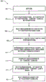
Referring to fig. 9, a method 400 of manufacturing an assembled PCB is shown in accordance with an illustrative embodiment. The method 400 may be implemented using the assembly 100 and PCB300 of fig. 4. Thus, the method 400 may be described with respect to fig. 1, 3, 4, 6, and 8A and 8B. In addition, the various steps of the method 400 are conceptually illustrated in fig. 10-17.
At 402, a substrate (e.g., substrate 102, etc.) is provided (see fig. 10). The substrate may define a plurality of ports (e.g., port 314, etc.). At 404, a plurality of guard rings (e.g., guard ring 318, etc.) are coupled to the substrate (see fig. 11). Each of the plurality of guard rings includes a portion (e.g., portion 332, etc.) along a first edge and an opposite second edge, the portion having a reduced thickness relative to the remaining edge. Block 404 may additionally include positioning each of the plurality of protective rings to surround a respective port of the plurality of ports and coupling each of the plurality of protective rings to the substrate with an adhesive or solder.
At 406, a plurality of MEMS transducers (e.g., MEMS transducer 118, etc.) are coupled to the substrate within a periphery of each guard ring of the plurality of guard rings (see fig. 12). For example, block 406 may include soldering the MEMS transducer to a microphone trace (e.g., microphone trace 316, etc.). Block 406 may additionally include aligning each MEMS transducer (e.g., an opening in each MEMS transducer) with a respective one of the ports. In some embodiments, block 406 may further include coupling an integrated circuit (e.g., integrated circuit 120, etc.) to the substrate (e.g., integrated circuit traces 312, etc.) within a periphery of each guard ring of the plurality of guard rings. In some embodiments, the plurality of MEMS transducers may be coupled to the substrate prior to coupling the plurality of protective rings to the substrate. In other embodiments, the plurality of MEMS transducers may be coupled to the substrate after the plurality of guard rings are coupled.
At 408, solder (e.g., solder 106, etc.) is applied to the substrate along a single axis between respective ones of the plurality of guard rings. In the embodiment shown in fig. 13, solder is applied to the substrate in a line along the X-axis direction (e.g., X-axis direction 306, etc.) to a second pair of edges (e.g., long edges, third edge 328 and fourth edge 330, etc.). Solder is applied at locations equally spaced from the longest edge of adjacent guard rings 318 such that an equal amount of solder is provided to each guard ring 318. Block 408 may include positioning a dispense needle (e.g., dispense needle 302, etc.) over the substrate, initiating a flow of solder through the needle, and moving the needle at a continuous rate along a serpentine path between adjacent rows of guard rings.
At 410, a cap (e.g., cap 104, etc.) is coupled to each of the plurality of protective rings to enclose each of the plurality of MEMS transducers and form a plurality of coupled microphone assemblies (see fig. 14). Block 410 may include providing a plurality of caps and positioning each cap of the plurality of caps over a respective MEMS transducer of the plurality of MEMS transducers such that a lower edge of each cap of the plurality of caps is aligned with a respective guard ring of the plurality of guard rings (e.g., such that each cap may cover at least a portion of a first edge and a second edge of a respective guard ring of the plurality of guard rings). Block 410 may further include pressing each of the plurality of caps into the solder to at least partially secure the cap in place relative to the substrate.
At 412, heat is applied to the solder to reflow the solder along the first and second edges of each of the plurality of protective rings (e.g., to reflow the solder into a gap between each of the plurality of caps and a respective one of the plurality of protective rings). Block 412 may include heating the entire assembled PCB including the substrate, MEMS transducer, integrated circuit, cap, and/or other assembly components to a peak temperature just above the melting temperature of the solder. Block 412 may include dwelling at the peak temperature for a predetermined period of time. For example, the assembled PCB may be placed in an oven or passed under an infrared lamp. Fig. 15-16 show top views of a single coupled microphone assembly before and after reflow processing, respectively. As shown in fig. 16, after heating, the solder reflows along the first and second edges 324, 326 of the guard ring. Solder along the first and second edges is hidden under the cover due to the reduced thickness of the first and second edges. In other embodiments, the solder along the first and second edges may protrude outward beyond the outer edge of the cap by a distance (e.g., a distance less than the distance between the outer edge of the cap and the outer edge of the solder along the third and fourth edges).
At 414, a plurality of labels (e.g., labels 108, etc.) are applied to the substrate. As shown in fig. 17, each of the plurality of labels is applied to a respective one of the first edge and the second edge and shared between adjacent components. Block 414 may include positioning a dispensing head for the label at a central location along a respective one of the first and second edges and dispensing at a predetermined flow rate for a predetermined period of time. Block 414 may additionally include curing the labels (e.g., dwell for a predetermined period of time) to ensure that each label is structurally robust. Further details regarding the application of labels to substrates can be found in U.S. patent No.10,227,232, which is incorporated herein by reference in its entirety. At 416, individual ones of the plurality of coupled microphone assemblies are separated (e.g., diced, etc.) from the assembled PCB to form a plurality of individual microphone assemblies. In some implementations, the method 400 may further include coupling the microphone assembly to an end-user device (e.g., a smartphone, a tablet, a laptop, etc.). In some implementations, the method 400 may include additional, fewer, and/or different operations.
The subject matter described herein sometimes illustrates different components contained within, or connected with, different other components. It is to be understood that such depicted architectures are exemplary, and that in fact many other architectures can be implemented which achieve the same functionality. In a conceptual sense, any arrangement of components to achieve the same functionality is effectively "associated" such that the desired functionality is achieved. Hence, any two components herein combined to achieve a particular functionality can be seen as "associated with" each other such that the desired functionality is achieved, irrespective of architectures or intermedial components. Likewise, any two components so associated can also be viewed as being "operably connected," or "operably coupled," to each other to achieve the desired functionality, and any two components capable of being so associated can also be viewed as being "operably couplable," to each other to achieve the desired functionality. Specific examples of operably couplable include, but are not limited to, physically mateable and/or physically interacting components and/or wirelessly interactable and/or wirelessly interacting components and/or logically interacting and/or logically interactable components.
With respect to the use of plural and/or singular terms herein, those having skill in the art can translate from the plural to the singular and/or from the singular to the plural as is appropriate to the context and/or application. Various singular/plural permutations may be expressly set forth herein for clarity.
It will be understood by those within the art that, in general, terms used herein, and especially in the appended claims (e.g., bodies of the appended claims) are generally intended as "open" terms (e.g., the term "including" should be interpreted as "including but not limited to," the term "having" should be interpreted as "having at least," the term "includes" should be interpreted as "includes but is not limited to," etc.).
Although the figures and description may illustrate a particular order of method steps, the order of the steps may differ from that depicted and described unless otherwise specified above. In addition, two or more steps may be performed simultaneously or partially simultaneously, unless otherwise specified above. Such variations may depend, for example, on the software and hardware systems selected and on designer choice. All such variations are within the scope of the present disclosure. Likewise, software implementations of the described methods can be accomplished with standard programming techniques with rule based logic and other logic to accomplish the various connection steps, processing steps, comparison steps and decision steps.
It will be further understood by those within the art that if a specific number of an introduced claim recitation is intended, such an intent will be explicitly recited in the claim, and in the absence of such recitation no such intent is present. For example, as an aid to understanding, the following appended claims may contain usage of the introductory phrases "at least one" and "one or more" to introduce claim recitations. However, the use of such phrases should not be construed to imply that the introduction of a claim recitation by the indefinite articles "a" or "an" limits any particular claim containing such introduced claim recitation to inventions containing only one such recitation, even when the same claim includes the introductory phrases "one or more" or "at least one" and indefinite articles such as "a" or "an" (e.g., "a" and/or "an" should typically be interpreted to mean "at least one" or "one or more"); the same holds true for the use of definite articles used to introduce claim recitations. In addition, even if a specific number of an introduced claim recitation is explicitly recited, those skilled in the art will recognize that such recitation should typically be interpreted to mean at least the recited number (e.g., the bare recitation of "two recitations," without other modifiers, typically means at least two recitations, or two or more recitations).
Also, in those instances where a convention analogous to "at least one of A, B and C, etc." is used, in general such a construction is intended in the sense one having skill in the art would understand the convention (e.g., "a system having at least one of A, B and C" would include, but not be limited to, systems that have a alone, B alone, C alone, a and B together, a and C together, B and C together, and/or A, B and C together, etc.). In those instances where a convention analogous to "A, B or at least one of C, etc." is used, in general, such a construction is intended in the sense one having skill in the art would conventionally understand the convention (e.g., "a system having at least one of A, B or C" would include, but not be limited to, systems that have a alone, B alone, C alone, a and B together, a and C together, B and C together, and/or A, B and C together, etc.). It will be further understood by those within the art that virtually any disjunctive word and/or phrase presenting two or more alternative terms, whether in the description, claims, or drawings, should be understood to contemplate the possibilities of including one of the terms, either of the terms, or both terms. For example, the phrase "a or B" will be understood to include the possibility of "a" or "B" or "a and B".
Moreover, unless otherwise specified, the use of the words "approximately," "about," "approximately," "substantially," and the like, refer to plus or minus ten percent.
The foregoing description of the exemplary embodiments has been presented for purposes of illustration and description. It is not intended to be exhaustive or to be limited to the precise form disclosed, and modifications and variations are possible in light of the above teachings or may be acquired from practice of the disclosed embodiments. It is intended that the scope of the invention be defined by the claims appended hereto and their equivalents.
Claims (16)
1. A microphone assembly, comprising:
a substrate defining a port;
a MEMS transducer coupled to the substrate such that the MEMS transducer is positioned over the port;
a guard ring coupled to the substrate and surrounding the MEMS transducer, the guard ring comprising a plurality of edges, wherein a portion of a first edge of the plurality of edges and a portion of an opposing second edge of the plurality of edges have a reduced thickness relative to an adjacent edge of the plurality of edges; and
a cap coupled to the protective ring such that the substrate and the cap collectively define an internal cavity.
2. The microphone assembly of claim 1, wherein the cover is coupled to the protective ring by solder, and wherein the solder extends along an entire length of only two of the plurality of edges.
3. The microphone assembly of claim 1, wherein the cover is coupled to the protective ring by solder, and wherein the solder is visible only along a portion of the first and second edges.
4. The microphone assembly of claim 1, wherein the plurality of edges define a frame, and wherein a thickness of the frame at each corner of the frame is greater than a thickness of the portion of the first edge and a thickness of the portion of the second edge.
5. The microphone assembly of claim 1, wherein the cover covers the first edge and the second edge such that the first edge and the second edge do not extend beyond an outer edge of the cover.
6. The microphone assembly of claim 1, wherein the plurality of edges further comprises a third edge and a fourth edge, wherein the third edge and the fourth edge are each perpendicular to the first edge and the second edge, and wherein a length of the third edge and the fourth edge is greater than a length of the first edge and the second edge.
7. The microphone assembly of claim 1, further comprising a plurality of labels, wherein each label of the plurality of labels is disposed on one of the first edge and the second edge.
8. The microphone assembly of claim 7, wherein each of the plurality of tabs is disposed at a central location along one of the first edge and the second edge.
9. The microphone assembly of claim 7, wherein the cover is coupled to the protective ring by solder, and wherein each of the plurality of tags comprises a material having a melting point higher than a melting point of the solder.
10. An assembled PCB, the assembled PCB comprising:
a substrate; and
a plurality of guard rings coupled to the substrate, each guard ring of the plurality of guard rings including a plurality of edges, wherein a first edge of the plurality of edges and an opposing second edge of the plurality of edges have a reduced thickness relative to an adjacent edge of the plurality of edges.
11. The assembled PCB of claim 10, wherein the plurality of edges of each guard ring further comprises a third edge and a fourth edge, wherein the third edge and the fourth edge are each perpendicular to the first edge and the second edge, and wherein a length of the third edge and the fourth edge is greater than a length of the first edge and the second edge.
12. The assembled PCB of claim 10, wherein the substrate further defines a plurality of ports, wherein the assembled PCB further comprises:
a plurality of MEMS transducers coupled to the substrate, each of the plurality of MEMS transducers positioned over a respective port of the plurality of ports, wherein each of the plurality of protective rings surrounds a respective MEMS transducer of the plurality of MEMS transducers; and
a plurality of shrouds, each shroud of the plurality of shrouds coupled to a respective protective ring of the plurality of protective rings to form an internal cavity.
13. The assembled PCB of claim 12, wherein each of the plurality of caps is coupled to a respective one of the plurality of protective rings by solder, and wherein the solder of each respective one of the plurality of protective rings extends along an entire length of only two of the plurality of edges.
14. The assembled PCB of claim 12, wherein each of the plurality of caps is coupled to a respective one of the plurality of protective rings by solder, and wherein the solder of each respective one of the plurality of protective rings extends only along an outer portion of the first and second edges.
15. The assembled PCB of claim 12, wherein each of the plurality of caps covers the first and second edges of a respective one of the plurality of protective rings such that the first and second edges do not extend beyond an outer edge of the cap.
16. The assembled PCB of claim 12, further comprising a plurality of tabs, each tab of a first plurality of tabs coupled to the first edge of a respective one of the plurality of caps, and each tab of a second plurality of tabs coupled to the second edge of a respective one of the plurality of caps.
Applications Claiming Priority (2)
| Application Number | Priority Date | Filing Date | Title |
|---|---|---|---|
| US201962898355P | 2019-09-10 | 2019-09-10 | |
| US62/898,355 | 2019-09-10 |
Publications (1)
| Publication Number | Publication Date |
|---|---|
| CN212660328U true CN212660328U (en) | 2021-03-05 |
Family
ID=74761759
Family Applications (1)
| Application Number | Title | Priority Date | Filing Date |
|---|---|---|---|
| CN202021960819.XU Active CN212660328U (en) | 2019-09-10 | 2020-09-09 | Microphone assembly and assembled PCB |
Country Status (2)
| Country | Link |
|---|---|
| US (1) | US11259133B2 (en) |
| CN (1) | CN212660328U (en) |
Cited By (1)
| Publication number | Priority date | Publication date | Assignee | Title |
|---|---|---|---|---|
| CN117459867A (en) * | 2023-12-07 | 2024-01-26 | 瑞声光电科技(常州)有限公司 | Microphone |
Family Cites Families (12)
| Publication number | Priority date | Publication date | Assignee | Title |
|---|---|---|---|---|
| US6710461B2 (en) * | 2002-06-06 | 2004-03-23 | Lightuning Tech. Inc. | Wafer level packaging of micro electromechanical device |
| US20090151972A1 (en) * | 2004-05-28 | 2009-06-18 | Stellar Microdevices, Inc. | Cold weld hermetic mems package and method of manufacture |
| WO2008067431A2 (en) * | 2006-11-30 | 2008-06-05 | Analog Devices, Inc. | Microphone system with silicon microphone secured to package lid |
| US9399574B2 (en) * | 2009-08-13 | 2016-07-26 | Knowles Electronics Llc | MEMS package and a method for manufacturing the same |
| US8384168B2 (en) * | 2011-04-21 | 2013-02-26 | Freescale Semiconductor, Inc. | Sensor device with sealing structure |
| US9368429B2 (en) * | 2011-10-25 | 2016-06-14 | Intel Corporation | Interposer for hermetic sealing of sensor chips and for their integration with integrated circuit chips |
| CN107258089A (en) * | 2014-12-23 | 2017-10-17 | 思睿逻辑国际半导体有限公司 | MEMS transducer package |
| CN106331965B (en) * | 2015-06-30 | 2019-09-13 | 意法半导体股份有限公司 | MEMS Microphone |
| US20170084521A1 (en) * | 2015-09-18 | 2017-03-23 | Industrial Technology Research Institute | Semiconductor package structure |
| US10227232B2 (en) | 2016-07-27 | 2019-03-12 | Knowles Electronics, Llc | Microelectromechanical system (MEMS) device packaging |
| DE112017006148B4 (en) * | 2016-12-05 | 2024-04-25 | Knowles Electronics, Llc | RAMPING SENSOR PERFORMANCE IN A MICROELECTROMECHANICAL SYSTEM DEVICE |
| US10314171B1 (en) * | 2017-12-29 | 2019-06-04 | Intel Corporation | Package assembly with hermetic cavity |
-
2020
- 2020-09-09 CN CN202021960819.XU patent/CN212660328U/en active Active
- 2020-09-10 US US17/017,120 patent/US11259133B2/en active Active
Cited By (1)
| Publication number | Priority date | Publication date | Assignee | Title |
|---|---|---|---|---|
| CN117459867A (en) * | 2023-12-07 | 2024-01-26 | 瑞声光电科技(常州)有限公司 | Microphone |
Also Published As
| Publication number | Publication date |
|---|---|
| US11259133B2 (en) | 2022-02-22 |
| US20210076149A1 (en) | 2021-03-11 |
Similar Documents
| Publication | Publication Date | Title |
|---|---|---|
| US10640371B2 (en) | Microelectromechanical system (MEMS) device packaging | |
| US8742569B2 (en) | Semiconductor package configured to electrically couple to a printed circuit board and method of providing same | |
| US8853564B2 (en) | Air cavity package configured to electrically couple to a printed circuit board and method of providing same | |
| US20060138626A1 (en) | Microelectronic packages using a ceramic substrate having a window and a conductive surface region | |
| JP2014168094A (en) | Micro electronic component package and method therefor | |
| TW200817278A (en) | Mems device and method of fabricating the same | |
| US6263563B1 (en) | Method of manufacturing and checking electronic components | |
| KR20160124323A (en) | Semiconductor device package and manufacturing method thereof | |
| CN212660328U (en) | Microphone assembly and assembled PCB | |
| CN102595293B (en) | Micro-electromechanical system (MEMS) microphone and packaging method thereof | |
| CN111422826B (en) | Method for manufacturing sensor | |
| CN109495831A (en) | A kind of encapsulating structure and its manufacturing method of MEMS microphone | |
| WO2007123300A1 (en) | Packaging structure of mems microphone | |
| EP3680211B1 (en) | Sensor unit and method of interconnecting a substrate and a carrier | |
| CN111422825B (en) | Method for manufacturing sensor | |
| KR102106170B1 (en) | Directional microphone package and method for manufacturing the same | |
| KR20050029926A (en) | Film bulk acoustic resonator and a manufacturing method thereof | |
| CN217468424U (en) | Integrated circuit package | |
| CN1983572A (en) | Semiconductor device and manufacturing method thereof | |
| JP2003060334A (en) | Mounted electronic circuit component | |
| CN113132837B (en) | Microphone assembly, circuit board, circuit board array, and method for manufacturing circuit board | |
| JP2002299520A (en) | Wiring boards and multi-cavity wiring boards | |
| JP7551806B2 (en) | Microphones and Electronics | |
| CN112624034B (en) | A MEMS device wafer-level packaging method and packaging structure | |
| JP3024608B2 (en) | Method for manufacturing semiconductor device |
Legal Events
| Date | Code | Title | Description |
|---|---|---|---|
| GR01 | Patent grant | ||
| GR01 | Patent grant |