CN211404907U - Electrical connector - Google Patents
Electrical connector Download PDFInfo
- Publication number
- CN211404907U CN211404907U CN202020201378.9U CN202020201378U CN211404907U CN 211404907 U CN211404907 U CN 211404907U CN 202020201378 U CN202020201378 U CN 202020201378U CN 211404907 U CN211404907 U CN 211404907U
- Authority
- CN
- China
- Prior art keywords
- electrical connector
- housing
- top cover
- substrate
- latch
- Prior art date
- Legal status (The legal status is an assumption and is not a legal conclusion. Google has not performed a legal analysis and makes no representation as to the accuracy of the status listed.)
- Active
Links
- 239000000758 substrate Substances 0.000 claims abstract description 27
- 230000013011 mating Effects 0.000 claims description 18
- 238000003780 insertion Methods 0.000 claims description 8
- 230000037431 insertion Effects 0.000 claims description 8
- PCHJSUWPFVWCPO-UHFFFAOYSA-N gold Chemical compound [Au] PCHJSUWPFVWCPO-UHFFFAOYSA-N 0.000 claims description 7
- 239000010931 gold Substances 0.000 claims description 7
- 229910052737 gold Inorganic materials 0.000 claims description 7
- 230000003014 reinforcing effect Effects 0.000 claims 2
- 230000014759 maintenance of location Effects 0.000 claims 1
- 229910000679 solder Inorganic materials 0.000 claims 1
- 238000000034 method Methods 0.000 description 6
- 238000005728 strengthening Methods 0.000 description 5
- 230000005540 biological transmission Effects 0.000 description 1
- 238000010586 diagram Methods 0.000 description 1
- 238000009826 distribution Methods 0.000 description 1
- 210000001503 joint Anatomy 0.000 description 1
- 238000004519 manufacturing process Methods 0.000 description 1
- 238000005476 soldering Methods 0.000 description 1
Images


Classifications
-
- H—ELECTRICITY
- H01—ELECTRIC ELEMENTS
- H01R—ELECTRICALLY-CONDUCTIVE CONNECTIONS; STRUCTURAL ASSOCIATIONS OF A PLURALITY OF MUTUALLY-INSULATED ELECTRICAL CONNECTING ELEMENTS; COUPLING DEVICES; CURRENT COLLECTORS
- H01R12/00—Structural associations of a plurality of mutually-insulated electrical connecting elements, specially adapted for printed circuits, e.g. printed circuit boards [PCB], flat or ribbon cables, or like generally planar structures, e.g. terminal strips, terminal blocks; Coupling devices specially adapted for printed circuits, flat or ribbon cables, or like generally planar structures; Terminals specially adapted for contact with, or insertion into, printed circuits, flat or ribbon cables, or like generally planar structures
- H01R12/70—Coupling devices
- H01R12/71—Coupling devices for rigid printing circuits or like structures
- H01R12/72—Coupling devices for rigid printing circuits or like structures coupling with the edge of the rigid printed circuits or like structures
- H01R12/721—Coupling devices for rigid printing circuits or like structures coupling with the edge of the rigid printed circuits or like structures cooperating directly with the edge of the rigid printed circuits
-
- H—ELECTRICITY
- H01—ELECTRIC ELEMENTS
- H01R—ELECTRICALLY-CONDUCTIVE CONNECTIONS; STRUCTURAL ASSOCIATIONS OF A PLURALITY OF MUTUALLY-INSULATED ELECTRICAL CONNECTING ELEMENTS; COUPLING DEVICES; CURRENT COLLECTORS
- H01R12/00—Structural associations of a plurality of mutually-insulated electrical connecting elements, specially adapted for printed circuits, e.g. printed circuit boards [PCB], flat or ribbon cables, or like generally planar structures, e.g. terminal strips, terminal blocks; Coupling devices specially adapted for printed circuits, flat or ribbon cables, or like generally planar structures; Terminals specially adapted for contact with, or insertion into, printed circuits, flat or ribbon cables, or like generally planar structures
- H01R12/70—Coupling devices
- H01R12/77—Coupling devices for flexible printed circuits, flat or ribbon cables or like structures
- H01R12/771—Details
-
- H—ELECTRICITY
- H01—ELECTRIC ELEMENTS
- H01R—ELECTRICALLY-CONDUCTIVE CONNECTIONS; STRUCTURAL ASSOCIATIONS OF A PLURALITY OF MUTUALLY-INSULATED ELECTRICAL CONNECTING ELEMENTS; COUPLING DEVICES; CURRENT COLLECTORS
- H01R13/00—Details of coupling devices of the kinds covered by groups H01R12/70 or H01R24/00 - H01R33/00
- H01R13/46—Bases; Cases
- H01R13/502—Bases; Cases composed of different pieces
-
- H—ELECTRICITY
- H01—ELECTRIC ELEMENTS
- H01R—ELECTRICALLY-CONDUCTIVE CONNECTIONS; STRUCTURAL ASSOCIATIONS OF A PLURALITY OF MUTUALLY-INSULATED ELECTRICAL CONNECTING ELEMENTS; COUPLING DEVICES; CURRENT COLLECTORS
- H01R13/00—Details of coupling devices of the kinds covered by groups H01R12/70 or H01R24/00 - H01R33/00
- H01R13/62—Means for facilitating engagement or disengagement of coupling parts or for holding them in engagement
- H01R13/627—Snap or like fastening
- H01R13/6271—Latching means integral with the housing
-
- H—ELECTRICITY
- H01—ELECTRIC ELEMENTS
- H01R—ELECTRICALLY-CONDUCTIVE CONNECTIONS; STRUCTURAL ASSOCIATIONS OF A PLURALITY OF MUTUALLY-INSULATED ELECTRICAL CONNECTING ELEMENTS; COUPLING DEVICES; CURRENT COLLECTORS
- H01R13/00—Details of coupling devices of the kinds covered by groups H01R12/70 or H01R24/00 - H01R33/00
- H01R13/62—Means for facilitating engagement or disengagement of coupling parts or for holding them in engagement
- H01R13/639—Additional means for holding or locking coupling parts together, after engagement, e.g. separate keylock, retainer strap
-
- H—ELECTRICITY
- H01—ELECTRIC ELEMENTS
- H01R—ELECTRICALLY-CONDUCTIVE CONNECTIONS; STRUCTURAL ASSOCIATIONS OF A PLURALITY OF MUTUALLY-INSULATED ELECTRICAL CONNECTING ELEMENTS; COUPLING DEVICES; CURRENT COLLECTORS
- H01R13/00—Details of coupling devices of the kinds covered by groups H01R12/70 or H01R24/00 - H01R33/00
- H01R13/646—Details of coupling devices of the kinds covered by groups H01R12/70 or H01R24/00 - H01R33/00 specially adapted for high-frequency, e.g. structures providing an impedance match or phase match
- H01R13/6461—Means for preventing cross-talk
- H01R13/6471—Means for preventing cross-talk by special arrangement of ground and signal conductors, e.g. GSGS [Ground-Signal-Ground-Signal]
-
- H—ELECTRICITY
- H01—ELECTRIC ELEMENTS
- H01R—ELECTRICALLY-CONDUCTIVE CONNECTIONS; STRUCTURAL ASSOCIATIONS OF A PLURALITY OF MUTUALLY-INSULATED ELECTRICAL CONNECTING ELEMENTS; COUPLING DEVICES; CURRENT COLLECTORS
- H01R12/00—Structural associations of a plurality of mutually-insulated electrical connecting elements, specially adapted for printed circuits, e.g. printed circuit boards [PCB], flat or ribbon cables, or like generally planar structures, e.g. terminal strips, terminal blocks; Coupling devices specially adapted for printed circuits, flat or ribbon cables, or like generally planar structures; Terminals specially adapted for contact with, or insertion into, printed circuits, flat or ribbon cables, or like generally planar structures
- H01R12/50—Fixed connections
- H01R12/59—Fixed connections for flexible printed circuits, flat or ribbon cables or like structures
- H01R12/62—Fixed connections for flexible printed circuits, flat or ribbon cables or like structures connecting to rigid printed circuits or like structures
-
- H—ELECTRICITY
- H01—ELECTRIC ELEMENTS
- H01R—ELECTRICALLY-CONDUCTIVE CONNECTIONS; STRUCTURAL ASSOCIATIONS OF A PLURALITY OF MUTUALLY-INSULATED ELECTRICAL CONNECTING ELEMENTS; COUPLING DEVICES; CURRENT COLLECTORS
- H01R13/00—Details of coupling devices of the kinds covered by groups H01R12/70 or H01R24/00 - H01R33/00
- H01R13/62—Means for facilitating engagement or disengagement of coupling parts or for holding them in engagement
- H01R13/629—Additional means for facilitating engagement or disengagement of coupling parts, e.g. aligning or guiding means, levers, gas pressure electrical locking indicators, manufacturing tolerances
- H01R13/633—Additional means for facilitating engagement or disengagement of coupling parts, e.g. aligning or guiding means, levers, gas pressure electrical locking indicators, manufacturing tolerances for disengagement only
- H01R13/6335—Additional means for facilitating engagement or disengagement of coupling parts, e.g. aligning or guiding means, levers, gas pressure electrical locking indicators, manufacturing tolerances for disengagement only comprising a handle
Landscapes
- Details Of Connecting Devices For Male And Female Coupling (AREA)
Abstract
The application discloses an electric connector, which comprises a substrate and a shell, wherein the substrate is provided with a plug-in part and a connecting part, the substrate is provided with a plurality of signal terminals and a plurality of grounding terminals which are arranged at intervals on at least one surface of the plug-in part, the edge of each signal terminal, which is far away from the connecting part, and the edge of each grounding terminal, which is far away from the connecting part, have a length difference, and the length difference is 0.3-0.5 mm; the shell covers the connecting part, the shell is provided with a top cover, and the top cover shields the surface of the substrate with the inserting part. The length difference between the grounding terminal and the signal terminal of the plugging part is set to be 0.3mm-0.5mm, so that the crosstalk generated among the terminals of the plugging part can be effectively reduced, and the volume of the substrate and the volume of the electric connector can be reduced.
Description
Technical Field
The present application relates to the field of connector technology, and more particularly, to an electrical connector.
Background
At present, a connector assembly includes a wire end connector and a board end connector, a substrate is disposed in the connector, and a plurality of gold fingers are distributed on the substrate, and the plurality of gold fingers are respectively a signal terminal and a ground terminal of the connector. The distance between the gold fingers or the length of the gold fingers can affect the transmission performance and the volume of the connector, and the current distribution mode of the gold fingers of the connector is easy to generate the problem of crosstalk.
SUMMERY OF THE UTILITY MODEL
The embodiment of the application provides an electric connector, which solves the problem that crosstalk easily occurs among a plurality of golden fingers of the existing electric connector.
In order to solve the technical problem, the present application is implemented as follows:
an electrical connector is provided, comprising: the substrate is provided with a plug part and a connecting part, a plurality of signal terminals and a plurality of ground terminals are arranged on at least one surface of the plug part at intervals, and the edge of each signal terminal, which is far away from the connecting part, and the edge of each ground terminal, which is far away from the connecting part, have a length difference of 0.3-0.5 mm; the shell covers the connecting part, the shell is provided with a top cover, and the top cover shields the surface of the substrate with the inserting part.
In the embodiment of the application, the length difference between the grounding terminal and the signal terminal of the plugging part is set to be 0.3mm-0.5mm, so that the crosstalk generated among the terminals of the plugging part can be effectively reduced, and meanwhile, the volume of the substrate can be reduced, and further, the volume of the electric connector is reduced.
Drawings
The accompanying drawings, which are included to provide a further understanding of the application and are incorporated in and constitute a part of this application, illustrate embodiment(s) of the application and together with the description serve to explain the application and not to limit the application. In the drawings:
fig. 1 is a perspective view of an electrical connector according to an embodiment of the present application;
FIG. 2 is a front view of an electrical connector according to one embodiment of the present application;
FIG. 3 is a schematic view of a substrate according to an embodiment of the present application;
FIG. 4 is an enlarged view of area A of FIG. 3;
FIG. 5 is a perspective view of a housing of an embodiment of the present application;
FIG. 6 is a front view of a housing of an embodiment of the present application.
Detailed Description
The technical solutions in the embodiments of the present application will be clearly and completely described below with reference to the drawings in the embodiments of the present application, and it is obvious that the described embodiments are some, but not all, embodiments of the present application. All other embodiments, which can be derived by a person skilled in the art from the embodiments given herein without making any creative effort, shall fall within the protection scope of the present application.
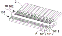
Please refer to fig. 1, 2 and 3, which are a perspective view, a front view and a schematic diagram of a substrate of an electrical connector according to an embodiment of the present application; as shown in the figure, the electrical connector 1 of the present embodiment includes a substrate 10 and a housing 11, the substrate 10 has a plug portion 101 and a connection portion 102, and the plug portion 101 and the connection portion 102 are respectively located at two ends of the substrate 10. The housing 11 covers the connecting portion 102 and has a top cover 111, and the top cover 111 extends toward the mating portion 101 and shields the surface of the substrate 10 having the mating portion 101. The housing 11 of the present embodiment has a body 112, the body 112 covers the connecting portion 102, the plug portion 101 protrudes from the body 112, and the top cover 111 is disposed on a side of the body 112 close to the plug portion 101.
The substrate 10 is provided with a plurality of signal terminals 1011 and a plurality of ground terminals 1012 on at least one surface of the inserting part 101, the plurality of signal terminals 1011 and the plurality of ground terminals 1012 are arranged at intervals, in this embodiment, a pair of signal terminals 1011 is provided between two adjacent ground terminals 1012, and a ground terminal is provided between two pairs of signal terminals 1011. Of course, more than one pair of signal terminals 1011 may be provided between two adjacent ground terminals 1012. The substrate 10 is also provided with a plurality of signal terminals and a plurality of ground terminals on at least one surface of the connection portion 102, and the plurality of signal terminals and the plurality of ground terminals of the connection portion 102 correspond to the plurality of signal terminals 1011 and the plurality of ground terminals 1012 of the plug portion 101. The substrate 10 of the present embodiment is a circuit board, the plurality of signal terminals 1011 and the plurality of ground terminals 1012 of the plugging portion 101 and the plurality of signal terminals and the plurality of ground terminals of the connecting portion 102 are gold fingers, respectively, and the plurality of signal terminals 1011 and the plurality of ground terminals 1012 of the plugging portion 101 are electrically connected to the plurality of signal terminals and the plurality of ground terminals of the connecting portion 102 through a circuit in the substrate 10. The connection portion 102 of the present embodiment is connected by soldering to the plurality of cables 2.
Please refer to FIG. 4, which is an enlarged view of area A in FIG. 3; as shown, each signal terminal 1011 has a first signal edge 1011a and a second signal edge 1011b, the first signal edge 1011a being opposite the second signal edge 1011 b. Each ground terminal 1012 has a first ground edge 1012a and a second ground edge 1012b, with first ground edge 1012a and second ground edge 1012b opposing each other. A length Ls between a first signal edge 1011a and a second signal edge 1011b of each signal terminal 1011 is smaller than a length Lg between a first ground edge 1012a and a second ground edge 1012b of each ground terminal 1012, the first signal edge 1011a of each signal terminal 1011 and the first ground edge 1012a of each ground terminal 1012 are close to the connection portion 102, and the second signal edge 1011b of each signal terminal 1011 and the second ground edge 1012b of each ground terminal 1012 are far from the connection portion 102. The first signal edge 1011a of each signal terminal 1011 is aligned with the first ground edge 1012a of each ground terminal 1012, and the second signal edge 1011b of each signal terminal 1011 and the second ground edge 1012b of each ground terminal 1012 have a length difference Ld between them, the length difference Ld being 0.3mm-0.5mm, i.e., the length difference Ld is greater than or equal to 0.3mm and less than or equal to 0.5 mm.
Preferably, the length difference Ld between the second signal edge 1011b of each signal terminal 1011 and the second ground edge 1012b of each ground terminal 1012 is 0.36mm-0.45mm, i.e., the length difference Ld is greater than or equal to 0.36mm and less than or equal to 0.45 mm.
Preferably, the length difference Ld between the second signal edge 1011b of each signal terminal 1011 and the second ground edge 1012b of each ground terminal 1012 is 0.38mm-0.42mm, i.e., the length difference Ld is greater than or equal to 0.38mm and less than or equal to 0.42 mm.
As can be seen from the above, the length of each ground terminal 1012 is greater than the length of each signal terminal 1011, so that crosstalk between the terminals can be avoided, and the length difference Ld between each signal terminal 1011 and each ground terminal 1012 is 0.3mm to 0.5mm, which effectively reduces the volume of the substrate 10 and thus the volume of the electrical connector 1.
Preferably, please refer to fig. 5 and 6 together, which are a perspective view and a front view of the housing according to an embodiment of the present application; as shown in the figure, the housing 11 has a baffle structure 113, the baffle structure 113 is disposed on the periphery of the main body 112, and the baffle structure 113 extends toward the insertion part 101 and is located around the insertion part 101. The insertion of the connector mated with the electrical connector 1 of the present embodiment is guided by the baffle structure 113, so that the housing of the mated connector is inserted between the baffle structure 113 and the body part 112 or/and between the baffle structure 113 and the top cover 111, and covers the top cover 111. The baffle structure 113 of the embodiment includes two side baffles 1131, the two side baffles 1131 are disposed on two opposite sides of the main body 112, and the two side baffles 1131 extend toward the insertion part 101 and are located on two sides of the insertion part 101. The side shield 1131 is used to guide at least a portion of the sidewall of the housing of the mated connector into the space between the side shield 1131 and the body portion 112 or/and the space between the side shield 1131 and the top cover 111.
Preferably, the baffle structure 113 of the embodiment further includes two upper baffles 1132, the two upper baffles 1132 are respectively disposed on the inner surfaces of the corresponding side baffles 1131 and are close to the top cover 111, and each upper baffle 1132 horizontally extends from the corresponding side baffle 1131 to the top cover 111. Each upper baffle 1132 of the present embodiment can shield the top cover 111 of the housing 11 of the wall portion. The upper baffle 1132 functions in the same way as the side baffles 1131, and guides the top wall of the housing of the mating connector between the upper baffle 1132 and the top cover 111.
Preferably, there is a retaining groove 114 between the baffle structure 113 and the body portion 112, in other words, the retaining groove 114 is located between each side baffle 1131 and the body portion 112 and between each upper baffle 1132 and the body portion 112. When the mating connector is inserted into the electrical connector 1 of this embodiment, the housing of the mating connector enters along the baffle structure 113, and a portion of the housing of the last mating connector is inserted into the limiting groove 114, so that the mating connector is accurately inserted into the electrical connector 1 of this embodiment, and the oblique insertion of the mating connector from the electrical connector 1 of this embodiment is avoided.
Preferably, each side guard 1131 has a slope 11311 on the side away from the top cover 111, and the slope 11311 forms an angle with the horizontal plane of the bottom side of the side guard 1131 away from the top cover 111, and the angle is smaller than 45 degrees. The electrical connector 1 of the present embodiment is inserted into the mating connector obliquely by the inclined surface 11311 of the side of each side guard 1131 away from the top cover 111, thereby increasing the degree of freedom of oblique insertion.
Preferably, each side guard 1131 has a positioning protrusion 11312 facing the inner surface of the substrate 10, and the positioning protrusion 11312 of the present embodiment has a plurality of positioning protrusions 11312a, and the extending direction of each positioning protrusion 11312a is parallel to the length direction of the substrate 10, i.e., each positioning protrusion 11312a extends from the body 112 to a direction away from the body 112. Of course, the positioning ribs 11312a may be replaced with bumps. The positioning protrusion 11312 can position the housing of the mating connector in the horizontal position of the electrical connector 1 of this embodiment, so as to prevent the housing of the mating connector from shaking left and right in the electrical connector 1 of this embodiment.
The electrical connector 1 of the present embodiment further includes a locking structure 12, and the locking structure 12 is disposed on an outer surface of the housing 11 having the top cover 111. The outer surface of the housing 11 having the top cover 111 has a latch receiving groove 115, and the latch structure 12 is disposed in the latch receiving groove 115. The locking structure 12 of the present embodiment includes a locking spring 121 and a pulling strip 122, the locking spring 121 is disposed in the locking receiving groove 115, and the pulling strip 122 is disposed at an end of the locking spring 121 far away from the inserting portion 101. The surface of the locking spring 121 away from the top cover 111 has a locking portion 1211. When the electrical connector 1 of the present embodiment is inserted into the mating connector, the housing of the mating connector covers the top cover 111 and is connected to the locking portion 1211 of the locking elastic piece 121, so as to fix the electrical connector 1 of the present embodiment to the mating connector.
Preferably, the inner surface of the housing 11 having the top cover 111 further has a strengthening portion 1111, the strengthening portion 1111 corresponds to the latch receiving groove 115, the strengthening portion 1111 protrudes from the inner surface of the housing 11 having the top cover 111 to the inside of the housing 11, and a height difference Hd is formed between the surface of the strengthening portion 1111 facing the inserting portion 101 and the inner surface of the housing 11 having the top cover 111, in other words, the thickness of the bottom surface of the latch receiving groove 115 is increased by the strengthening portion 1111, so as to enhance the structural strength of the latch receiving groove 115.
Preferably, the inner surface of the top cover 111 has two shrink-proof grooves 1112, the two shrink-proof grooves 1112 of the present embodiment are respectively located at two sides of the lock accommodating groove 115, so as to prevent the housing 11 from shrinking during manufacturing, and further prevent the side of the top cover 111 from warping.
In summary, the present application provides an electrical connector, which can effectively reduce crosstalk generated between a plurality of terminals of a plugging portion by setting a length difference between a ground terminal and a signal terminal of the plugging portion to 0.3mm-0.5mm, and can also reduce a volume of a substrate, thereby reducing the volume of the electrical connector. The shell is further provided with a baffle structure which can guide the electric connector of the application to be inserted into the butted connector. One side that the top cap was kept away from to the baffle structure has the inclined plane, makes the electric connector of this application insert in the connector of butt joint to one side, increases the degree of freedom of inserting to one side. The inner surface of the baffle structure is provided with a positioning convex part, so that when the electric connector and the butting connector are used, the butting connector is prevented from deviating in the electric connector, and meanwhile, the friction force between the butting connector and the butting connector is reduced, so that the butting connector is smoothly connected with the electric connector.
It should be noted that, in this document, the terms "comprises," "comprising," or any other variation thereof, are intended to cover a non-exclusive inclusion, such that a process, method, article, or apparatus that comprises a list of elements does not include only those elements but may include other elements not expressly listed or inherent to such process, method, article, or apparatus. Without further limitation, an element defined by the phrase "comprising an … …" does not exclude the presence of other like elements in a process, method, article, or apparatus that comprises the element.
While the present embodiments have been described with reference to the accompanying drawings, it is to be understood that the invention is not limited to the precise embodiments described above, which are meant to be illustrative and not restrictive, and that various changes may be made therein by those skilled in the art without departing from the spirit and scope of the invention as defined by the appended claims.
Claims (17)
1. An electrical connector, comprising:
the substrate is provided with a plug part and a connecting part, a plurality of signal terminals and a plurality of ground terminals are arranged on at least one surface of the plug part at intervals, and a length difference is formed between the edge of each signal terminal far away from the connecting part and the edge of each ground terminal far away from the connecting part and is 0.3-0.5 mm;
the shell covers the connecting part and is provided with a top cover which shields the surface of the substrate with the inserting part.
2. The electrical connector of claim 1, wherein the housing has a baffle structure positioned around the mating part.
3. The electrical connector of claim 2, wherein said shield structure includes two side shields, said two side shields being positioned on opposite sides of said mating portion.
4. The electrical connector of claim 3, wherein each of said side dams has a beveled surface on a side thereof remote from said top cover.
5. The electrical connector of claim 3, wherein the inner surface of each of said side dams has a locating boss.
6. The electrical connector of claim 3, wherein said baffle structure further comprises two top baffles, said top baffles being disposed on an inner surface of each of said side baffles, said top baffles extending horizontally from said side baffles toward said top cover.
7. The electrical connector of claim 6, wherein each of said top shields said top cover of said housing of a portion.
8. The electrical connector of any one of claims 2-7, wherein the housing has a body portion, the mating portion projects from the body portion, and a retention groove is provided between the baffle structure and the body portion.
9. The electrical connector of claim 1, further comprising a latching structure disposed on an outer surface of the housing.
10. The electrical connector of claim 9, wherein the outer surface of the housing has a latch receiving slot, and the latch structure is disposed in the latch receiving slot.
11. The electrical connector of claim 10, wherein the inner surface of the housing further has a reinforcing portion corresponding to the latch receiving groove, and a height difference exists between a surface of the reinforcing portion facing the mating portion and the inner surface of the housing.
12. The electrical connector of claim 10, wherein the latch structure comprises a latch leaf and a pull strip, the latch leaf is disposed in the latch receiving groove, and the pull strip is disposed at an end of the latch leaf away from the insertion portion.
13. The electrical connector of claim 1, wherein the substrate is a circuit board.
14. The electrical connector of claim 13, wherein each of the plurality of signal terminals and the plurality of ground terminals is a gold finger.
15. The electrical connector of claim 1, wherein the inner surface of the top cover has a shrink-proof groove.
16. The electrical connector of claim 1, wherein the connecting portion is solder connected to a plurality of wires.
17. The electrical connector of claim 1, wherein the length difference is 0.36-0.45 mm.
Priority Applications (2)
| Application Number | Priority Date | Filing Date | Title |
|---|---|---|---|
| CN202020201378.9U CN211404907U (en) | 2020-02-24 | 2020-02-24 | Electrical connector |
| US16/923,874 US11233359B2 (en) | 2020-02-24 | 2020-07-08 | Electrical connector |
Applications Claiming Priority (1)
| Application Number | Priority Date | Filing Date | Title |
|---|---|---|---|
| CN202020201378.9U CN211404907U (en) | 2020-02-24 | 2020-02-24 | Electrical connector |
Publications (1)
| Publication Number | Publication Date |
|---|---|
| CN211404907U true CN211404907U (en) | 2020-09-01 |
Family
ID=72209653
Family Applications (1)
| Application Number | Title | Priority Date | Filing Date |
|---|---|---|---|
| CN202020201378.9U Active CN211404907U (en) | 2020-02-24 | 2020-02-24 | Electrical connector |
Country Status (2)
| Country | Link |
|---|---|
| US (1) | US11233359B2 (en) |
| CN (1) | CN211404907U (en) |
Cited By (3)
| Publication number | Priority date | Publication date | Assignee | Title |
|---|---|---|---|---|
| CN112103723A (en) * | 2020-10-09 | 2020-12-18 | 东莞立讯技术有限公司 | Terminal structure and electric connector |
| TWI872768B (en) * | 2023-03-30 | 2025-02-11 | 貝爾威勒電子股份有限公司 | Cable-end connector |
| US12463361B2 (en) | 2022-05-12 | 2025-11-04 | Dongguan Luxshare Technologies Co., Ltd | Electrical connector with improved reliability, connector assembly, and method of making electrical connector |
Families Citing this family (9)
| Publication number | Priority date | Publication date | Assignee | Title |
|---|---|---|---|---|
| US11303065B2 (en) * | 2019-09-07 | 2022-04-12 | Dongguan Luxshare Technologies Co., Ltd | Low profile first connector, second connector and connector assembly |
| TWM593098U (en) * | 2019-12-05 | 2020-04-01 | 貿聯國際股份有限公司 | Wire connector and electronic device connection system having the same |
| TWM595899U (en) * | 2019-12-06 | 2020-05-21 | 貿聯國際股份有限公司 | Circuit board structure and connector having the same |
| CN111403932B (en) * | 2020-04-24 | 2025-01-21 | 东莞立讯技术有限公司 | Wire end connector |
| CN212257885U (en) * | 2020-07-15 | 2020-12-29 | 莫列斯有限公司 | Connector and electric connecting device |
| CN116191124B (en) * | 2021-11-29 | 2025-10-21 | 电连技术股份有限公司 | Socket connectors and connector assemblies |
| CN114976774A (en) * | 2022-05-25 | 2022-08-30 | 吉安鸿呈电子有限公司 | An electrical connector structure and preparation process thereof |
| USD1078642S1 (en) * | 2022-11-11 | 2025-06-10 | Dongguan Luxshare Technologies Co., Ltd | Adaptor connector |
| TWI845358B (en) * | 2023-06-26 | 2024-06-11 | 宏致電子股份有限公司 | Plug connector and its matching socket connector |
Family Cites Families (15)
| Publication number | Priority date | Publication date | Assignee | Title |
|---|---|---|---|---|
| US7267575B1 (en) * | 2007-02-07 | 2007-09-11 | Uniconn Corp. | Structure of signal cable connector |
| CN201562831U (en) * | 2008-09-09 | 2010-08-25 | 莫列斯公司 | Connector with impedance tuning terminal arrangement |
| US7857650B1 (en) * | 2009-06-15 | 2010-12-28 | Hon Hai Precision Ind. Co., Ltd. | Electrical connector assembly with latching mechanism |
| CN203574938U (en) | 2013-10-24 | 2014-04-30 | 安费诺电子装配(厦门)有限公司 | PCB with goldfingers and connector for transmission line |
| CN205724167U (en) * | 2016-05-06 | 2016-11-23 | 富士康(昆山)电脑接插件有限公司 | Electric connector |
| DE102016108989A1 (en) * | 2016-05-13 | 2017-11-16 | Erni Production Gmbh & Co. Kg | Plug contact set and method for checking a latching of the plug contact set |
| US9728876B1 (en) * | 2016-11-04 | 2017-08-08 | Cen Link Co., Ltd. | Electric connector |
| CN108321591B (en) * | 2017-01-14 | 2021-02-26 | 富士康(昆山)电脑接插件有限公司 | Electrical connector |
| TWM551363U (en) * | 2017-01-23 | 2017-11-01 | 宣德科技股份有限公司 | Improvement of the connector structure |
| CN207677189U (en) | 2018-01-16 | 2018-07-31 | 安费诺电子装配(厦门)有限公司 | A kind of connector assembly |
| CN208209042U (en) | 2018-03-30 | 2018-12-07 | 安费诺电子装配(厦门)有限公司 | A kind of small-sized ultrahigh speed wire and cable connector and connector assembly |
| CN209266665U (en) | 2018-07-25 | 2019-08-16 | 安费诺电子装配(厦门)有限公司 | A kind of ultra high speed signal wire and cable connector |
| US10756468B2 (en) * | 2018-11-07 | 2020-08-25 | Bellwether Electronic Corp. | Plug connector assembly, flexible flat cable assembly thereof, and flexible flat cable thereof |
| US11189971B2 (en) * | 2019-02-14 | 2021-11-30 | Amphenol East Asia Ltd. | Robust, high-frequency electrical connector |
| TWM584035U (en) * | 2019-06-18 | 2019-09-21 | 貝爾威勒電子股份有限公司 | Plug connector with protective member for replacing gold finger of circuit board |
-
2020
- 2020-02-24 CN CN202020201378.9U patent/CN211404907U/en active Active
- 2020-07-08 US US16/923,874 patent/US11233359B2/en active Active
Cited By (4)
| Publication number | Priority date | Publication date | Assignee | Title |
|---|---|---|---|---|
| CN112103723A (en) * | 2020-10-09 | 2020-12-18 | 东莞立讯技术有限公司 | Terminal structure and electric connector |
| US11749949B2 (en) | 2020-10-09 | 2023-09-05 | Dongguan Luxshare Technologies Co., Ltd | Terminal assembly and electrical connector |
| US12463361B2 (en) | 2022-05-12 | 2025-11-04 | Dongguan Luxshare Technologies Co., Ltd | Electrical connector with improved reliability, connector assembly, and method of making electrical connector |
| TWI872768B (en) * | 2023-03-30 | 2025-02-11 | 貝爾威勒電子股份有限公司 | Cable-end connector |
Also Published As
| Publication number | Publication date |
|---|---|
| US20210265782A1 (en) | 2021-08-26 |
| US11233359B2 (en) | 2022-01-25 |
Similar Documents
| Publication | Publication Date | Title |
|---|---|---|
| CN211404907U (en) | Electrical connector | |
| US7086901B2 (en) | Shielded electrical connector | |
| CN107404033B (en) | Electric connector and manufacturing method thereof | |
| US8337247B2 (en) | Power electrical connector with improved metallic shell | |
| CN210137059U (en) | Plug connector of small high-speed flat cable | |
| EP0224200A2 (en) | Shielded plug and jack connector | |
| US6210230B1 (en) | Cable connector | |
| CN110391518B (en) | Electrical connector | |
| US7473133B1 (en) | Electrical connector | |
| TWM597991U (en) | Plug connector of miniature high speed flat cable | |
| US8033866B2 (en) | Receptacle connector having reinforced bracket increasing overall rigidity | |
| CN104078799B (en) | Middle relay connector | |
| CN114976729A (en) | Cable connector with improved shielding member | |
| CN212392412U (en) | Board end connector and connector assembly | |
| CN114024172A (en) | Cable connector and connector assembly | |
| CN113937571A (en) | A connector with terminal module | |
| CN217387647U (en) | Electrical connector | |
| CN209981537U (en) | Electrical connector | |
| CN210156593U (en) | Electrical connector | |
| CN201029176Y (en) | electrical connector | |
| US6666714B1 (en) | Electrical connector with terminal protector | |
| CN212392408U (en) | Terminal structure and connector | |
| CN114784548A (en) | electrical connector | |
| CN113394598A (en) | Electrical connector | |
| CN213753310U (en) | Card edge connector |
Legal Events
| Date | Code | Title | Description |
|---|---|---|---|
| GR01 | Patent grant | ||
| GR01 | Patent grant | ||
| TR01 | Transfer of patent right |
Effective date of registration: 20211206 Address after: 518104 2nd floor, building a, Sanyang new industrial zone, HO-1 West, Shajing street, Bao'an District, Shenzhen City, Guangdong Province Patentee after: LUXSHARE PRECISION INDUSTRY Co.,Ltd. Address before: Room 401, building 2, No.5, information road, Songshanhu Park, Dongguan City, Guangdong Province 523808 Patentee before: Dongguan Lixun Technology Co.,Ltd. |
|
| TR01 | Transfer of patent right |