CN210780527U - IGBT drive circuit of wind power converter - Google Patents
IGBT drive circuit of wind power converter Download PDFInfo
- Publication number
- CN210780527U CN210780527U CN201921709854.1U CN201921709854U CN210780527U CN 210780527 U CN210780527 U CN 210780527U CN 201921709854 U CN201921709854 U CN 201921709854U CN 210780527 U CN210780527 U CN 210780527U
- Authority
- CN
- China
- Prior art keywords
- circuit
- drive
- isolation
- optocoupler
- vce
- Prior art date
- Legal status (The legal status is an assumption and is not a legal conclusion. Google has not performed a legal analysis and makes no representation as to the accuracy of the status listed.)
- Active
Links
- 238000002955 isolation Methods 0.000 claims abstract description 40
- 238000001514 detection method Methods 0.000 claims abstract description 19
- 238000004804 winding Methods 0.000 claims description 3
- 238000005070 sampling Methods 0.000 description 6
- 230000000903 blocking effect Effects 0.000 description 2
- 230000003111 delayed effect Effects 0.000 description 2
- 239000013307 optical fiber Substances 0.000 description 2
- 230000007704 transition Effects 0.000 description 2
- 230000009286 beneficial effect Effects 0.000 description 1
- 230000008878 coupling Effects 0.000 description 1
- 238000010168 coupling process Methods 0.000 description 1
- 238000005859 coupling reaction Methods 0.000 description 1
- 238000010586 diagram Methods 0.000 description 1
- 238000000034 method Methods 0.000 description 1
Images


Landscapes
- Power Conversion In General (AREA)
Abstract
本实用新型公开了风电变流器的IGBT驱动电路,包括原边电路、隔离电路和副边电路,原边电路包括死区电路、互锁电路、保护电路、15V电源输入滤波电路和DC/DC电路,隔离电路包括变压器隔离电路和光耦隔离电路,副边电路包括±15V驱动电源、驱动电路和Vce‑sat检测电路,本实用新型能够有效保护IGBT模块,并且该实用新型原边电路集成了死区电路、互锁电路和保护电路,可以提高抗干扰能力,提高驱动电路可靠性。
The utility model discloses an IGBT drive circuit of a wind power converter, which comprises a primary side circuit, an isolation circuit and a secondary side circuit. The primary side circuit comprises a dead zone circuit, an interlock circuit, a protection circuit, a 15V power input filter circuit and a DC/DC circuit. Circuit, the isolation circuit includes a transformer isolation circuit and an optocoupler isolation circuit, and the secondary circuit includes a ±15V drive power supply, a drive circuit and a Vce-sat detection circuit. The utility model can effectively protect the IGBT module, and the primary side circuit of the utility model integrates a dead circuit. Zone circuit, interlock circuit and protection circuit can improve the anti-interference ability and improve the reliability of the drive circuit.
Description
技术领域technical field
本实用新型涉及驱动电路技术领域,具体是风电变流器的IGBT驱动电路。The utility model relates to the technical field of driving circuits, in particular to an IGBT driving circuit of a wind power converter.
背景技术Background technique
风电变流器系统电压690V,一般采用1700V的IGBT模块,大功率IGBT模块开关速度快,产生很高的di/dt和du/dt,带来EMC电磁干扰问题,影响变流器的可靠运行,甚至损坏IGBT模块,为了提高抗干扰能力,有以下两种解决方案:The voltage of the wind power converter system is 690V, and the IGBT module of 1700V is generally used. The high-power IGBT module has a fast switching speed and generates high di/dt and du/dt, which brings EMC electromagnetic interference problems and affects the reliable operation of the converter. Even damage the IGBT module, in order to improve the anti-interference ability, there are the following two solutions:
1)、采用光纤传递控制信号,控制电路弱信号与IGBT模块的强信号实现电气完全隔离,抗干扰能力强,可靠性高,但是光纤成本昂贵;1) Using optical fiber to transmit control signals, the weak signal of the control circuit and the strong signal of the IGBT module are completely electrically isolated, with strong anti-interference ability and high reliability, but the cost of optical fiber is expensive;
2)、通常采用专用的驱动器和驱动芯片,例如风电专用驱动器2SD300,采用专业的调制与解调芯片,通过脉冲变压器传递驱动信号,抗干扰能力强,可靠性高,大量应用于风电变流器领域。2), usually use special drivers and driving chips, such as wind power special driver 2SD300, which adopts professional modulation and demodulation chips, transmits driving signals through pulse transformers, has strong anti-interference ability and high reliability, and is widely used in wind power converters field.
以上两种方案虽然解决了风电变流器EMC抗干扰问题,但是成本相对较高,较为经济的解决方案是采用光耦来实现电气隔离,但是光耦的原边一般采用低压电路(15V或者5V),容易受干扰。Although the above two solutions solve the EMC anti-interference problem of wind power converters, the cost is relatively high. The more economical solution is to use optocouplers to achieve electrical isolation, but the primary side of optocouplers generally uses low-voltage circuits (15V or 5V). ), easily disturbed.
另外,大功率IGBT模块在运行过程中产生高的di/dt和du/dt,会导致IGBT模块上下管门极误触发,导致IGBT模块上下管直通,产生短路电流,如果不及时保护就会导致IGBT模块损坏,严重影响变流器正常运行。In addition, the high di/dt and du/dt generated by the high-power IGBT module during operation will cause false triggering of the upper and lower transistor gates of the IGBT module, resulting in direct connection of the upper and lower transistors of the IGBT module, resulting in short-circuit current. If it is not protected in time, it will lead to The IGBT module is damaged, which seriously affects the normal operation of the converter.
实用新型内容Utility model content
本实用新型的目的在于提供风电变流器的IGBT驱动电路,以解决上述背景技术中提出的问题。The purpose of the present invention is to provide an IGBT drive circuit of a wind power converter, so as to solve the above-mentioned problems in the background art.
为实现上述目的,本实用新型提供如下技术方案:To achieve the above object, the utility model provides the following technical solutions:
风电变流器的IGBT驱动电路,包括原边电路、隔离电路和副边电路,所述原边电路包括死区电路、互锁电路、保护电路、15V电源输入滤波电路和DC/DC电路,所述隔离电路包括变压器隔离电路和光耦隔离电路,所述副边电路包括±15V驱动电源、驱动电路和Vce-sat检测电路,Vce-sat检测电路分别连接IGBT模块、驱动电路和光耦隔离电路,光耦隔离电路还连接死区电路、互锁电路和保护电路,驱动电路还分别连接光耦隔离电路和IGBT模块,Vce-sat检测电路检测到IGBT模块发生短路故障或过流故障时,通过光耦隔离电路传递故障信号给原边电路,原边电路同时封锁IGBT模块上下管驱动信号,并通过光耦隔离电路和驱动电路关断IGBT模块。The IGBT drive circuit of the wind power converter includes a primary side circuit, an isolation circuit and a secondary side circuit. The primary side circuit includes a dead zone circuit, an interlock circuit, a protection circuit, a 15V power input filter circuit and a DC/DC circuit. The isolation circuit includes a transformer isolation circuit and an optocoupler isolation circuit. The secondary side circuit includes a ±15V drive power supply, a drive circuit and a Vce-sat detection circuit. The Vce-sat detection circuit is respectively connected to the IGBT module, the drive circuit and the optocoupler isolation circuit. The coupling isolation circuit is also connected to the dead zone circuit, the interlock circuit and the protection circuit, and the drive circuit is also connected to the optocoupler isolation circuit and the IGBT module respectively. When the Vce-sat detection circuit detects that the IGBT module has a short-circuit fault or an overcurrent fault, the The isolation circuit transmits the fault signal to the primary side circuit, the primary side circuit blocks the driving signal of the upper and lower tubes of the IGBT module at the same time, and turns off the IGBT module through the optocoupler isolation circuit and the driving circuit.
作为本实用新型的进一步方案:所述IGBT模块分为上下两路。As a further solution of the present invention: the IGBT module is divided into upper and lower circuits.
作为本实用新型的进一步方案:所述死区电路、互锁电路、保护电路均分为上下两路。As a further solution of the present invention, the dead zone circuit, the interlock circuit and the protection circuit are divided into upper and lower circuits.
作为本实用新型的进一步方案:所述光耦隔离电路分为上下两路。As a further solution of the present invention: the optocoupler isolation circuit is divided into upper and lower circuits.
作为本实用新型的进一步方案:所述驱动电路分为上下两路。As a further solution of the present invention: the drive circuit is divided into upper and lower circuits.
作为本实用新型的进一步方案:所述光耦隔离电路包括反馈光耦和驱动光耦。As a further solution of the present invention, the optocoupler isolation circuit includes a feedback optocoupler and a driving optocoupler.
作为本实用新型的进一步方案:所述变压器隔离电路采用高频隔离变压器,其副边有两个独立的绕组,输出两路隔离电源。As a further scheme of the present utility model: the transformer isolation circuit adopts a high-frequency isolation transformer, the secondary side has two independent windings, and outputs two isolated power sources.
与现有技术相比,本实用新型的有益效果是:本实用新型能够有效保护IGBT模块,并且该实用新型原边电路集成了死区电路、互锁电路和保护电路,可以提高抗干扰能力,提高驱动电路可靠性。Compared with the prior art, the beneficial effects of the utility model are: the utility model can effectively protect the IGBT module, and the primary side circuit of the utility model integrates the dead zone circuit, the interlock circuit and the protection circuit, which can improve the anti-interference ability, Improve the reliability of the drive circuit.
附图说明Description of drawings
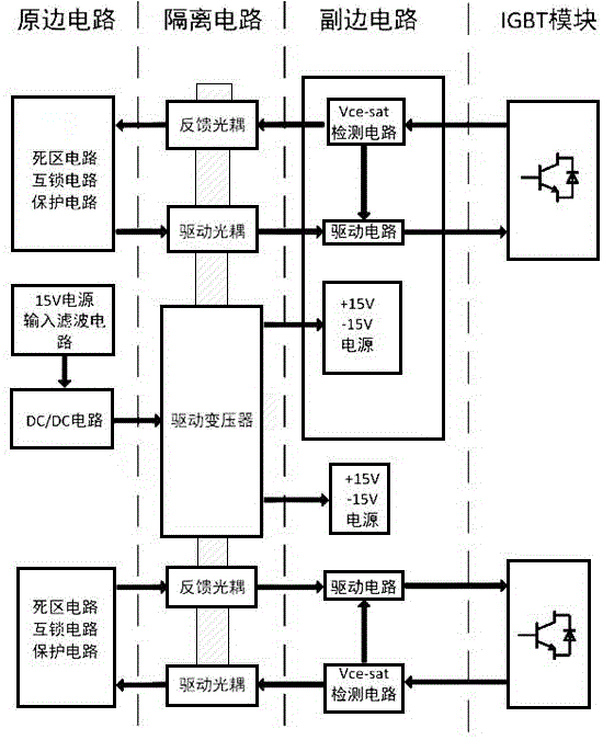
图1为本实用新型涉及的风电变流器驱动电路示意图。FIG. 1 is a schematic diagram of a drive circuit of a wind power converter according to the present invention.
图2为本实用新型涉及的风电变流器的具体驱动电路。FIG. 2 is a specific drive circuit of the wind power converter according to the present invention.
具体实施方式Detailed ways
下面将结合本实用新型实施例中的附图,对本实用新型实施例中的技术方案进行清楚、完整地描述,显然,所描述的实施例仅仅是本实用新型一部分实施例,而不是全部的实施例。基于本实用新型中的实施例,本领域普通技术人员在没有做出创造性劳动前提下所获得的所有其他实施例,都属于本实用新型保护的范围。The technical solutions in the embodiments of the present utility model will be clearly and completely described below with reference to the accompanying drawings in the embodiments of the present utility model. Obviously, the described embodiments are only a part of the embodiments of the present utility model, rather than all the implementations. example. Based on the embodiments of the present invention, all other embodiments obtained by those of ordinary skill in the art without creative work fall within the protection scope of the present invention.
请参阅图1-2,实施例1:本实用新型实施例中,风电变流器的IGBT驱动电路,包括原边电路、隔离电路和副边电路,原边电路包括死区电路、互锁电路、保护电路、15V电源输入滤波电路和DC/DC电路,隔离电路包括变压器隔离电路和光耦隔离电路,副边电路包括±15V驱动电源、驱动电路和Vce-sat检测电路。Please refer to Fig. 1-2, Embodiment 1: In the embodiment of the present utility model, the IGBT drive circuit of the wind power converter includes a primary side circuit, an isolation circuit and a secondary side circuit, and the primary side circuit includes a dead zone circuit and an interlock circuit , protection circuit, 15V power input filter circuit and DC/DC circuit, isolation circuit includes transformer isolation circuit and optocoupler isolation circuit, secondary circuit includes ±15V drive power supply, drive circuit and Vce-sat detection circuit.
原边电路包括上下管的死区电路、互锁电路和保护电路;The primary side circuit includes the dead zone circuit, interlock circuit and protection circuit of the upper and lower tubes;
死区电路的作用是:实现上下管驱动信号有一定的时间间隔Td,例如上管驱动信号关闭后,需要等待Td延时后才能开通下管驱动信号;The function of the dead zone circuit is to realize that the upper and lower tube driving signals have a certain time interval Td. For example, after the upper tube driving signal is turned off, it is necessary to wait for the Td delay before turning on the lower tube driving signal;
互锁电路的作用是:上下管驱动信号不能同时为有效,避免产生上下管驱动直通信号;The function of the interlock circuit is: the upper and lower tube driving signals cannot be effective at the same time, so as to avoid the generation of the upper and lower tube driving straight-through signals;
保护电路的作用是:当副边出现故障信号是,保护电路能够同时关闭上下管驱动信号。The function of the protection circuit is: when there is a fault signal on the secondary side, the protection circuit can turn off the driving signals of the upper and lower tubes at the same time.
15V电源输入滤波电路的作用是:对输入15V电源进行滤波,维持15V电源的稳定并且降低EMC干扰。The function of the 15V power input filter circuit is to filter the
DC/DC电路的的作用是:15V电源高频脉宽调制DC/DC。The role of the DC/DC circuit is: 15V power supply high frequency pulse width modulation DC/DC.
隔离电路包括:驱动光耦、反馈光耦和隔离变压器。The isolation circuit includes: drive optocoupler, feedback optocoupler and isolation transformer.
驱动光耦的作用是:传递原边驱动信号给副边电路,电气隔离原边低压侧和副边高压侧。The function of the driving optocoupler is to transmit the primary side driving signal to the secondary side circuit, and electrically isolate the primary side low voltage side and the secondary side high voltage side.
反馈光耦的作用是:传递副边故障信号给原边电路,电气隔离原边低压侧和副边高压侧。The function of the feedback optocoupler is to transmit the fault signal of the secondary side to the circuit of the primary side, and electrically isolate the low-voltage side of the primary side and the high-voltage side of the secondary side.
隔离变压器的作用是:输出上下管驱动电源,电气隔离原边低压侧和副边高压侧。The function of the isolation transformer is to output the driving power of the upper and lower tubes, and electrically isolate the low-voltage side of the primary side and the high-voltage side of the secondary side.
副边电路包括:±15V电源、驱动电路、Vce-sat检测电路。The secondary side circuit includes: ±15V power supply, drive circuit, Vce-sat detection circuit.
±15V电源的作用是:输出IGBT模块所推荐的驱动电源。The function of the ±15V power supply is to output the drive power recommended by the IGBT module.
驱动电路的作用是:副边驱动信号放大,推挽输出。The function of the drive circuit is to amplify the secondary side drive signal and push-pull output.
Vce-sat检测电路的作用是:检测IGBT模块退饱和或过流信号,故障信号反馈给原边。The function of the Vce-sat detection circuit is to detect the desaturation or overcurrent signal of the IGBT module, and the fault signal is fed back to the primary side.
Vce-sat检测电路分别连接IGBT模块、驱动电路和光耦隔离电路,光耦隔离电路还连接死区电路、互锁电路和保护电路,驱动电路还分别连接光耦隔离电路和IGBT模块,Vce-sat检测电路检测到IGBT模块发生短路故障或过流故障时,通过光耦隔离电路传递故障信号给原边电路,原边电路同时封锁IGBT模块上下管驱动信号,并通过光耦隔离电路和驱动电路关断IGBT模块。The Vce-sat detection circuit is connected to the IGBT module, the drive circuit and the optocoupler isolation circuit respectively. The optocoupler isolation circuit is also connected to the dead zone circuit, the interlock circuit and the protection circuit. The drive circuit is also connected to the optocoupler isolation circuit and the IGBT module. Vce-sat When the detection circuit detects that the IGBT module has a short-circuit fault or an overcurrent fault, it transmits the fault signal to the primary circuit through the optocoupler isolation circuit. Turn off the IGBT module.
实施例2:在实施例1的基础上,本实用新型的一种实施例电路如图2所示,Embodiment 2: On the basis of Embodiment 1, an embodiment circuit of the present utility model is shown in FIG. 2 ,
其中,15V电源输入滤波电路由L1和C1构成的滤波器,其作用主要是:对输入15V电源进行滤波,并且降低开关噪声和电磁干扰。Among them, the 15V power input filter circuit is a filter composed of L1 and C1, and its main function is to filter the
DC/DC电路由Q1,Q2,T1构成推挽电路,并且Q1和Q2由晶体管构成,T1为高频隔离变压器,其副边有两个独立的绕组,输出两路隔离电源:The DC/DC circuit is composed of Q1, Q2, T1 to form a push-pull circuit, and Q1 and Q2 are composed of transistors. T1 is a high-frequency isolation transformer, and its secondary side has two independent windings, which output two isolated power supplies:
其中上管隔离电源包括:The top-tube isolated power supply includes:
D7与C4构成二极管整流电路,输出-15V_SH电源;D7 and C4 form a diode rectifier circuit and output -15V_SH power supply;
D8与C5构成二极管整流电路,输出+15V_SH电源;D8 and C5 form a diode rectifier circuit and output +15V_SH power supply;
其中下管隔离电源包括:Among them, the lower tube isolated power supply includes:
D9与C6构成二极管整流电路,输出-15V_SL电源;D9 and C6 form a diode rectifier circuit and output -15V_SL power supply;
D11与C7构成二极管整流电路,输出+15V_SL电源;D11 and C7 form a diode rectifier circuit and output +15V_SL power supply;
上管死区电路和互锁电路由V1,V2,R2,C2,D2组成,下管死区电路和互锁电路由V3,V4,R3,C3,D3组成,保护电路包括D5,V5,D6,V6构成。The upper tube dead zone circuit and interlock circuit are composed of V1, V2, R2, C2, D2, the lower tube dead zone circuit and interlock circuit are composed of V3, V4, R3, C3, D3, and the protection circuit includes D5, V5, D6 , V6 composition.
PWM_H信号为上管输入信号,PWM_L信号为下管输入信号;The PWM_H signal is the input signal of the upper tube, and the PWM_L signal is the input signal of the lower tube;
当PWM_L信号为高电平时,C2通过D2快速放电,PWM_L信号为低电平时,C2通过R2充电,R2,C2构成死区延时Td。When the PWM_L signal is at a high level, C2 discharges quickly through D2, and when the PWM_L signal is at a low level, C2 is charged through R2, and R2 and C2 form a dead zone delay Td.
当PWM_H信号为高电平时,C3通过D3快速放电,PWM_L信号为低电平时,C3通过R3充电,R3,C3构成死区延时Td。When the PWM_H signal is at a high level, C3 is rapidly discharged through D3, and when the PWM_L signal is at a low level, C3 is charged through R3, and R3 and C3 form a dead zone delay Td.
其中V1输入采用CMOS施密特与非门,可以提高输入信号门槛电压,提高信号抗干扰能力。Among them, the V1 input adopts CMOS Schmitt NAND gate, which can improve the threshold voltage of the input signal and improve the anti-interference ability of the signal.
上管驱动电路由R11,Q3,Q4,R8构成推挽放大电路,对光耦输出信号U2_OUT信号进行放大,上管驱动信号DRV_H直接连接IGBT模块上管门极HG,满足IGBT模块对于驱动峰值电流的需求。The upper tube drive circuit is composed of R11, Q3, Q4, R8 to form a push-pull amplifier circuit, which amplifies the optocoupler output signal U2_OUT signal, and the upper tube drive signal DRV_H is directly connected to the upper tube gate HG of the IGBT module to meet the IGBT module's drive peak current. demand.
下管驱动电路由R17,Q5,Q6,R18构成推挽放大电路,对光耦输出信号U4_OUT信号进行放大,下管驱动信号DRV_L直接连接IGBT模块下管门极LG,满足IGBT模块对于驱动峰值电流的需求。The lower tube drive circuit consists of R17, Q5, Q6, R18 to form a push-pull amplifier circuit, which amplifies the optocoupler output signal U4_OUT signal, and the lower tube drive signal DRV_L is directly connected to the lower tube gate LG of the IGBT module, which meets the IGBT module's drive peak current. demand.
上管Vce-sat检测电路由R9,D11,R10构成Vce-sat采样电路:The upper tube Vce-sat detection circuit consists of R9, D11, R10 to form a Vce-sat sampling circuit:
当驱动信号DRV_H为高电平(15V)时,通过电阻和IGBT模块导通压降Vce-sat的分
压原理:

当驱动信号DRV_L为低电平(-15V)时,通过电阻和IGBT模块导通压降Vce-sat的分
压原理:
下管Vce-sat检测电路由R15,D12,R16构成Vce-sat采样电路:The lower tube Vce-sat detection circuit consists of R15, D12, R16 to form a Vce-sat sampling circuit:
当驱动信号DRV_L为高电平(15V)时,通过电阻和IGBT模块导通压降Vce-sat的分
压原理:

当驱动信号DRV_H为低电平(-15V)时,通过电阻和IGBT模块导通压降Vce-sat的分
压原理:
当FAULT_H为低电平时,光耦U1_OUT输出高电平,经过D5和V5后故障信号FAULT_P为低电平,对驱动信号进行封锁。When FAULT_H is low level, the optocoupler U1_OUT outputs high level, after D5 and V5, the fault signal FAULT_P is low level, which blocks the drive signal.
下管Vce-sat检测电路由R15,D12,R16构成Vce-sat采样电路,采样信号VCE_L,R13和R14构成分压电路(通过R13和R14设定保护值),比较信号COMP_L,通过VCE_L与COMP_L的比较实现Vce-sat的检测,并输出故障信号FAULT_L,当FAULT_L为低电平时,光耦U3_OUT输出高电平,经过D6和V6后故障信号FAULT_P为低电平,对驱动信号进行封锁。The lower tube Vce-sat detection circuit consists of R15, D12, R16 to form a Vce-sat sampling circuit, the sampling signals VCE_L, R13 and R14 form a voltage divider circuit (the protection value is set by R13 and R14), the comparison signal COMP_L, through VCE_L and COMP_L The comparison of Vce-sat realizes the detection of Vce-sat, and outputs the fault signal FAULT_L. When FAULT_L is low, the optocoupler U3_OUT outputs high level. After D6 and V6, the fault signal FAULT_P is low, and the driving signal is blocked.
上管信号的逻辑关系是:The logical relationship of the upper tube signal is:

其中V1_OUT是V1与非门的输出信号,U2_OUT是光耦U2的输出信号(上图对应U2的7脚)Among them, V1_OUT is the output signal of the V1 NAND gate, and U2_OUT is the output signal of the optocoupler U2 (the figure above corresponds to the 7-pin of U2)

死区逻辑说明:当模态2过渡到模态3时,中间至少要延时TdDead zone logic description: When mode 2 transitions to mode 3, at least Td should be delayed in the middle
互锁逻辑说明:当PWM_H和PWM_L同时为高电平时, U2输出信号为低电平,即避免了因EMC电磁干扰等因素导致IGBT模块上下管直通短路的情况,提高了原边电路的抗干扰能力,有效地保护了IGBT模块。Interlock logic description: When PWM_H and PWM_L are high at the same time, the U2 output signal is low, which avoids the direct short-circuit of the upper and lower tubes of the IGBT module due to EMC electromagnetic interference and other factors, and improves the anti-interference of the primary circuit. ability to effectively protect the IGBT module.
故障状态时,PWM_H和PWM_L是任意电平,驱动输出信号DRV_H为低电平,及时关断IGBT模块;In the fault state, PWM_H and PWM_L are at any level, and the drive output signal DRV_H is at a low level, and the IGBT module is turned off in time;
下管信号的逻辑关系是:The logical relationship of the down pipe signal is:

其中V3_OUT是V3与非门的输出信号,U4_OUT是光耦U4的输出信号(上图对应U4的7脚)Among them, V3_OUT is the output signal of the V3 NAND gate, and U4_OUT is the output signal of the optocoupler U4 (the figure above corresponds to pin 7 of U4)

死区逻辑说明:当模态2过渡到模态3时,中间至少要延时TdDead zone logic description: When mode 2 transitions to mode 3, at least Td should be delayed in the middle
互锁逻辑说明:当PWM_H和PWM_L同时为高电平时, U4输出信号为低电平,即避免了因EMC电磁干扰等因素导致IGBT模块上下管直通短路的情况,提高了原边电路的抗干扰能力,有效地保护了IGBT模块。Interlock logic description: When PWM_H and PWM_L are high at the same time, the U4 output signal is low, which avoids the direct short-circuit of the upper and lower tubes of the IGBT module due to EMC electromagnetic interference and other factors, and improves the anti-interference of the primary circuit. ability to effectively protect the IGBT module.
故障状态时,PWM_H和PWM_L是任意电平,驱动输出信号DRV_L为低电平,及时关断IGBT模块。In the fault state, PWM_H and PWM_L are at any level, and the drive output signal DRV_L is at a low level, which turns off the IGBT module in time.
对于本领域技术人员而言,显然本实用新型不限于上述示范性实施例的细节,而且在不背离本实用新型的精神或基本特征的情况下,能够以其他的具体形式实现本实用新型。因此,无论从哪一点来看,均应将实施例看作是示范性的,而且是非限制性的,本实用新型的范围由所附权利要求而不是上述说明限定,因此旨在将落在权利要求的等同要件的含义和范围内的所有变化囊括在本实用新型内。不应将权利要求中的任何附图标记视为限制所涉及的权利要求。It will be apparent to those skilled in the art that the present invention is not limited to the details of the above-described exemplary embodiments, and that the present invention may be implemented in other specific forms without departing from the spirit or essential characteristics of the present invention. Therefore, the embodiments are to be considered in all respects as exemplary and not restrictive, and the scope of the present invention is defined by the appended claims rather than the foregoing description, and it is therefore intended that the All changes within the meaning and range of the required equivalents are embraced within the present invention. Any reference signs in the claims shall not be construed as limiting the involved claim.
此外,应当理解,虽然本说明书按照实施方式加以描述,但并非每个实施方式仅包含一个独立的技术方案,说明书的这种叙述方式仅仅是为清楚起见,本领域技术人员应当将说明书作为一个整体,各实施例中的技术方案也可以经适当组合,形成本领域技术人员可以理解的其他实施方式。In addition, it should be understood that although this specification is described in terms of embodiments, not each embodiment only includes an independent technical solution, and this description in the specification is only for the sake of clarity, and those skilled in the art should take the specification as a whole , the technical solutions in each embodiment can also be appropriately combined to form other implementations that can be understood by those skilled in the art.
Claims (5)
Priority Applications (1)
| Application Number | Priority Date | Filing Date | Title |
|---|---|---|---|
| CN201921709854.1U CN210780527U (en) | 2019-10-14 | 2019-10-14 | IGBT drive circuit of wind power converter |
Applications Claiming Priority (1)
| Application Number | Priority Date | Filing Date | Title |
|---|---|---|---|
| CN201921709854.1U CN210780527U (en) | 2019-10-14 | 2019-10-14 | IGBT drive circuit of wind power converter |
Publications (1)
| Publication Number | Publication Date |
|---|---|
| CN210780527U true CN210780527U (en) | 2020-06-16 |
Family
ID=71039848
Family Applications (1)
| Application Number | Title | Priority Date | Filing Date |
|---|---|---|---|
| CN201921709854.1U Active CN210780527U (en) | 2019-10-14 | 2019-10-14 | IGBT drive circuit of wind power converter |
Country Status (1)
| Country | Link |
|---|---|
| CN (1) | CN210780527U (en) |
Cited By (1)
| Publication number | Priority date | Publication date | Assignee | Title |
|---|---|---|---|---|
| CN110635670A (en) * | 2019-10-14 | 2019-12-31 | 浙江日风电气股份有限公司 | A kind of IGBT driving circuit of wind power converter |
-
2019
- 2019-10-14 CN CN201921709854.1U patent/CN210780527U/en active Active
Cited By (1)
| Publication number | Priority date | Publication date | Assignee | Title |
|---|---|---|---|---|
| CN110635670A (en) * | 2019-10-14 | 2019-12-31 | 浙江日风电气股份有限公司 | A kind of IGBT driving circuit of wind power converter |
Similar Documents
| Publication | Publication Date | Title |
|---|---|---|
| CN103178694B (en) | Insulated gate bipolar transistor gate driving push-pull circuit | |
| CN108173419B (en) | A High Efficiency Driving Circuit for Wide Bandgap Power Devices | |
| CN103346763B (en) | A kind of igbt Drive Protecting Circuit | |
| CN204633582U (en) | Intelligent digital high-power IGBT driver | |
| CN105811942B (en) | A kind of MOSFET driving circuit and its application method with overcurrent protection function | |
| CN111641330B (en) | A driving circuit and a motor controller | |
| CN100574102C (en) | The processing method of IGBT driver and drive signal thereof | |
| CN109861505B (en) | IGBT driving circuit topological structure suitable for high-speed frequency converter | |
| WO2013174137A1 (en) | Drive circuit of insulated gate bipolar transistor | |
| CN110635670A (en) | A kind of IGBT driving circuit of wind power converter | |
| CN110620573A (en) | Drive circuit for power semiconductor switch | |
| CN113676029A (en) | Active clamping circuit based on IGBT | |
| CN203608076U (en) | A high voltage IGVT driving and protection circuit | |
| CN105356728A (en) | Isolated drive circuit | |
| CN205377644U (en) | Three level IGBT drive circuit on T type | |
| CN110289601A (en) | Active clamp circuit built into driver IC for protection of IGBT | |
| CN103546020A (en) | High-voltage IGBT driving and protecting circuit | |
| CN102710103B (en) | Double-circuit high-voltage large power IGBT (Insulated Gate Bipolar Translator) drive circuit | |
| CN210780527U (en) | IGBT drive circuit of wind power converter | |
| CN203180759U (en) | Gate driving push-pull circuit of insolated gate bipolar transistor | |
| CN105720802A (en) | H bridge full-function IGBT isolation driving control module | |
| CN110176855A (en) | A kind of active clamp protection circuit of the IGBT driving based on HCPL-316J | |
| CN203233299U (en) | IGBT drive circuit for braking of urban rail vehicle traction converter | |
| CN204424877U (en) | A kind of IGBT module Over Current Protection System | |
| CN203775066U (en) | T-type three-level three-phase inverter driving system |
Legal Events
| Date | Code | Title | Description |
|---|---|---|---|
| GR01 | Patent grant | ||
| GR01 | Patent grant | ||
| PE01 | Entry into force of the registration of the contract for pledge of patent right | ||
| PE01 | Entry into force of the registration of the contract for pledge of patent right |
Denomination of utility model: IGBT driving circuit of wind power converter Granted publication date: 20200616 Pledgee: Zhejiang Hangzhou Yuhang Rural Commercial Bank Co.,Ltd. Science and Technology City Branch Pledgor: ZHEJIANG HRV ELECTRIC Co.,Ltd. Registration number: Y2024980009884 |
|
| PC01 | Cancellation of the registration of the contract for pledge of patent right | ||
| PC01 | Cancellation of the registration of the contract for pledge of patent right |
Granted publication date: 20200616 Pledgee: Zhejiang Hangzhou Yuhang Rural Commercial Bank Co.,Ltd. Science and Technology City Branch Pledgor: ZHEJIANG HRV ELECTRIC Co.,Ltd. Registration number: Y2024980009884 |