SUMMERY OF THE UTILITY MODEL
To address at least the deficiencies of the prior art described in the background section above, the present invention provides a power module comprising an AC-DC chip having a plurality of pads and configured to perform management and control of the power module; and a transient voltage suppression diode chip having a plurality of pins connected to the AC-DC chip, wherein the AC-DC chip and the transient voltage suppression diode chip are integrated within a package having a plurality of pins, and wherein associated pads of the AC-DC chip and associated pins of the transient voltage suppression diode chip are connected to associated pins of the package to achieve a power output in operation.
In one embodiment, the AC-DC chip includes a mosfet to store energy in an energy storage element by controlling the switching of the mosfet.
In another embodiment, the power supply module includes a freewheeling diode chip connected outside the package, wherein the transient voltage suppression diode chip is connected at one end to a high-voltage control terminal among the plurality of pins of the package and at another end to the freewheeling diode chip outside the package.
In yet another embodiment, the power supply module includes a freewheeling diode chip integrated within the package, wherein the transient voltage suppression diode chip and the freewheeling diode chip are connected to a high-voltage control terminal and a high-voltage terminal of a plurality of pins of the package.
In one embodiment, the power module further comprises a mosfet chip integrated within the package, wherein one pad on the AC-DC chip is connected to a gate of the mosfet chip and a drain of the mosfet chip is connected to a high voltage control terminal among the pins of the package.
In another embodiment, the power supply module further comprises a freewheeling diode chip integrated within the package, wherein the transient voltage suppression diode chip and the freewheeling diode chip are connected to the high voltage control terminal and the high voltage terminal of the plurality of pins of the package.
In yet another embodiment, the power supply module further comprises a freewheeling diode chip connected outside the package, wherein the transient voltage suppression diode chip has one end connected to a high voltage terminal of the plurality of pins of the package and another end connected to the freewheeling diode chip outside the package.
In another embodiment, the power module further includes a rectifier diode circuit outside the package body having a plurality of pins connected to the AC-DC chip and configured to convert an input alternating current to a direct current.
Through the above-mentioned description to the utility model discloses a scheme and a plurality of embodiments thereof, technical personnel in the field can understand the utility model discloses a power module can form an solitary integrated circuit in a packaging body through integrated transient voltage suppression diode chip and AC-DC chip, has overcome among the prior art because difference and the degree of difficulty on the production technology and be difficult to integrate both in single chip simultaneously for power module after the miniaturization can be more extensive in the application to various lighting apparatus, has promoted the competitiveness of whole product. Additionally, utilize the utility model discloses a scheme can be with circuits such as the illumination of minimality mode control drive LED banks and charger, consequently the utility model discloses a scheme also is suitable for to circuit board volume and cost have multiple AC-DC power fields such as LED lighting drive, cell-phone charger of higher requirement.
Detailed Description
The utility model discloses to prior art not enough, provide a brand-new realizable solution. In particular, different use requirements are met by flexible chip combination integration. Those skilled in the art will appreciate from the following description that the present invention relates to various embodiments of power modules (or power module groups). Modifications and substitutions to the exemplary circuit structures or connections of the invention may be made by those skilled in the art, in light of the teachings of the present disclosure, and still fall within the scope of the invention, which is defined by the appended claims.
The present invention generally provides an AC-DC chip, TVS (tube or chip) and freewheeling diode (or chip) combined integrated as a circuit module for LED driving or charger driving. The module comprises a package with a plurality of pins, inside which e.g. up to six separate copper frames and eight separate chips can be arranged. The AC-DC chip is assembled by adopting a separate copper lead frame, so that the high-voltage isolation structure has good heat dissipation and safe high-voltage isolation efficiency. In one or more embodiments, the freewheeling diode and the TVS tube also use a copper lead frame as a carrier, at least two pads, and are also structurally supported by the outer leads, thereby providing good heat dissipation performance.
In an embodiment, the utility model discloses an integrated chip structure can be integrated to the module with freewheeling diode and TVS simultaneously, and encapsulation pin quantity after the integration can also be compatible completely with the pin function for driving circuit board has higher integrated level, and better price/performance ratio has enlarged power module's application scope and the flexibility of using, thereby is particularly suitable for in LED illumination and the portable cell-phone charger that have higher requirement to power board volume and cost.
Embodiments of the present invention will be described below in detail with reference to the accompanying drawings.
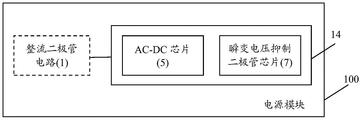
Fig. 4 is a circuit schematic diagram illustrating the power module 100 according to the present invention. As shown in fig. 4, the power module 100 of the present invention includes an AC-DC chip (or referred to as an IC power management chip) 5 and a transient voltage suppressing diode (TVS) chip 7. The AC-DC chip 5 may be provided with a plurality of pads and configured to perform management and control of the power module 100, while the TVS chip has a plurality of pins connected to the AC-DC chip. According to the present invention, the AC-DC chip 5 and the transient voltage suppression diode (TVS) chip 7 are integrated in a package 14 (e.g., a plastic package) having a plurality of pins, and the AC-DC chip 5 and the TVS chip 7 are connected to the associated pins of the package 14 through associated pads and pins, so as to realize power output, such as driving an LED circuit or charging an external portable device, in operation. In one embodiment, the rectifier diode circuit 1 (e.g., a high voltage rectifier bridge circuit) has a plurality of pins connected to the package 14 and is configured to convert an input ac power to a dc power.
Fig. 5 is a block diagram illustrating a power module according to an embodiment of the present invention. The power supply block shown in this block diagram modifies the circuit configuration shown in fig. 1 to provide a linear control drive scheme. The power module described in this embodiment is not only suitable for driving the LED lamp set with high efficiency, but also suitable for application in a charger.
As shown in fig. 5, the circuit configuration does not integrate a rectifier bridge diode, but includes an AC-DC chip (including MOSFET)5, a TVS chip 7, and a freewheeling diode chip 6, which are integrated in a package 14. The package body 14 has a plurality of pins and is internally provided with the aforementioned three chips, at least two lead frames 11, 12 having independent pads, and a plurality of metal leads 13. The AC-DC chip 5 can be functionally connected to the circuit by means of copper frame soldering or silver paste bonding and a plurality of bonding wires, and provides four pins, the copper frame being provided with at least two pads. In an exemplary connection, one pad on the AC-DC chip 5 may be connected to a high voltage terminal (HV) of the package 14 via a wire bond, which may be shared with a rectifier bridge circuit or the high voltage terminal of the chip outside the package. Further, one pad on the AC-DC chip 5 may be connected to a high voltage control pin (DRAIN) of the package 14 by a bonding wire, and the ground pad of the AC-DC chip 5 and the diode rectifying chip common terminal are connected to a common ground terminal (GND) by a bonding wire. In addition, the sampling terminal of the AC-DC chip 5 is externally connected to a terminal (CS) via a bonding wire. The TVS chip 7 and the freewheel diode chip 6 may be connected to a high voltage terminal (HV) and a high voltage control terminal (DRAIN) of the package 14 by means of two internal copper pads and bonding wires. The circuit has simple structure, higher output capability and better reliability.
Fig. 6 is a structural view illustrating a power module according to another embodiment of the present invention. The power supply module shown in this block diagram modifies the circuit configuration shown in fig. 3 to provide an isolated control drive scheme.
As shown in fig. 6, the power supply module includes an AC-DC chip 5 (including MOSFET) and a freewheeling diode 6 chip integrated in a package 14. The package 14 has a plurality of pins and is internally provided with lead frames 11, 12 including the two chips, at least two bonding pads, and a plurality of metal leads 13. In an exemplary connection, the AC-DC chip 5 may be functionally connected to the circuit by copper frame soldering or silver paste bonding and a plurality of bonding wires, one pad on the AC-DC chip 5 is connected to a high voltage terminal (HV) of the package 14 by a bonding wire, and another pad on the AC-DC chip 5 is connected to a high voltage control terminal (DRAIN) of the package by a bonding wire. The ground pad of the AC-DC chip 5 and the common ground of the diode rectifying chip may be connected to a common Ground (GND) through a bonding wire, and the sampling terminal of the AC-DC chip 5 is externally connected to a terminal (CS) through a bonding wire. One pad on the freewheeling diode chip 6 may be linked to the high-voltage control terminal DRAIN of the package 14 by a bonding lead.
Fig. 7 is a structural view illustrating a power module according to still another embodiment of the present invention. The power supply module shown in this block diagram modifies the circuit configuration shown in fig. 3 to provide isolated control drive.
As shown in fig. 7, the power module includes an AC-DC chip (including MOSFET)5 and a TVS chip 7 integrated in a package 14. The package 14 has a plurality of pins and is internally provided with the two chips, the lead frames 11 and 12 with at least two bonding pads, and a plurality of metal leads 13. In an exemplary connection, the AC-DC chip 5 achieves functional connection of the circuit by copper frame soldering or silver paste bonding and a plurality of bonding wires. One pad on the AC-DC chip 5 is connected to a high voltage terminal (HV) of the package 14 by a bonding wire, and the other pad on the AC-DC chip 5 is connected to a high voltage control terminal (DRAIN) of the package by a bonding wire. In addition, the ground pad of the AC-DC chip 5 may be connected to a common Ground (GND) through a bonding wire with a common ground of a diode rectifying circuit or a chip (such as a rectifying bridge circuit shown in the drawing) outside the package, and the sampling terminal of the AC-DC chip 5 is externally connected to one terminal (CS) through a bonding wire. One pad on TVS chip 7 may be linked to the high voltage terminal (HV) of the package by a bond wire.
Fig. 8 is a structural view illustrating a power module according to still another embodiment of the present invention. The power supply module shown in this block diagram modifies the circuit configuration shown in fig. 3 to provide isolated control drive. This circuit module does not have integrated rectifier bridge diode in the packaging body equally to the AC-DC chip of adoption does not contain the MOSFET transistor, but uses independent MOSFET transistor, makes the utility model discloses a power module has bigger driving force, thereby more is suitable for high-power LED drive and the application of the quick charger of heavy current.
As shown in fig. 8, the power supply module includes a separate AC-DC chip 5, a discrete power MOSFET transistor chip 15, a TVS chip 7 and a freewheeling diode chip 6, which are integrated in a package 14. The package body 14 has a plurality of pins and is internally provided with the aforementioned four chips, at least three lead frames with independent pads, and a plurality of metal leads 13. At least four pins of the external lead have defined functions, and other pins improve heat dissipation and physical functions. In an exemplary connection, the AC-DC chip 5 may be functionally connected to the circuit by copper frame soldering or silver paste bonding and a plurality of bonding wires, wherein one pad on the AC-DC chip 5 is connected to the high voltage terminal (HV) of the package 14 by the bonding wire, and one pad on the AC-DC chip 5 is connected to the gate (G) of the MOSFET transistor by the bonding wire. Further, the ground pad of the AC-DC chip 5 is connected to the common ground terminal (GND) by a bonding wire, and the sampling terminal of the AC-DC chip 5 is externally connected to a terminal (CS) by a bonding wire. The freewheeling diode chip 6 and the TVS chip 7 can be connected to the high voltage terminal (HV) and the high voltage control terminal (DRAIN) of the package 14 by means of two internal copper pads and bonding wires. The gate of the individual MOSFET transistor chip 15 can be controlled by a signal of the AC-DC chip 5 through a bonding wire, its source (S) can be connected to pin CS through a bonding wire, and its DRAIN (D) is connected to a high voltage control terminal (DRAIN) of the package 14 through a lead frame.
Fig. 9 is a structural view showing a power module according to still another embodiment of the present invention. The power supply module shown in this block diagram modifies the circuit configuration shown in fig. 3 to provide isolated control drive. Specifically, the power supply module includes an AC-DC chip 5, a MOSFET chip 15, and a freewheeling diode 6, which are integrated in one package to form a single integrated circuit.
As shown in fig. 9, the package body 14 has a plurality of pins and is internally provided with the aforementioned three chips, at least three lead frames 11, 12, 16 with pads, and a plurality of metal leads 13. The AC-DC chip 5 can realize the functional connection of the circuit by copper frame soldering or silver paste bonding and a plurality of bonding wires. In one exemplary connection, one pad on the AC-DC chip 5 is connected to the high voltage terminal (HV) of the package 14 by a bonding wire, and the other pad is connected to the MOSFET gate (G) by a bonding wire. Further, the ground pad of the AC-DC chip 5 and the common ground terminal of the diode rectifying chip or circuit outside the package body are connected to the common ground terminal (GND) of the package body 14 through a bonding wire, and the sampling terminal of the AC-DC chip 5 may be externally connected to a terminal (CS) through a bonding wire. The drain of the MOSFET may be connected to the DRAIM terminal. The freewheeling diode chip 6 may be soldered to the frame pad and connected to the TVS tube outside the package 14, and the front side of the chip may be linked to the high voltage control terminal (DRAIN) of the package 14 by bonding wires.
Fig. 10 is a structural view illustrating a power module according to another embodiment of the present invention. The power supply module shown in this block diagram modifies the circuit configuration shown in fig. 3 to provide an isolated drive scheme. Specifically, the power supply module includes one AC-DC chip 5, one MOSFET chip 15, and one TVS chip 7, which are integrated in one package to form a single integrated circuit.
As shown in fig. 10, the package body 14 has a plurality of pins and is internally provided with the aforementioned three chips, at least three lead frames 11, 12, 16 with pads, and a plurality of metal leads 13. In an exemplary connection, the AC-DC chip 5 may be functionally connected to the circuit by means of copper frame soldering or silver paste bonding and a plurality of bonding wires. One pad on the AC-DC chip 5 may be connected to a high voltage terminal (HV) of the package 14 by a bonding wire, and the other pad of the AC-DC chip 5 is connected to a MOSFET gate (G) by a bonding wire. Further, the ground pad of the AC-DC chip 5 may be connected to a common ground pin (GND) of the package 14 through a bonding wire with a common ground of a diode rectifying chip or circuit outside the package 14, and the sampling terminal of the AC-DC chip 5 may be externally connected to a terminal (CS) through a bonding wire. The drain of the MOSFET may be connected to the high voltage control terminal (DRAIM) of the package 14, while the TVS chip 7 may be soldered to the frame pad and connected to a freewheeling diode outside the package 14, and the front side of the chip may be linked to the high voltage terminal (HV) of the package 14 by bonding wires.
From the above detailed description, those skilled in the art can understand that in the above-described embodiments of the present invention and in various embodiments thereof, the rectifier diode chip or the rectifier bridge circuit may be used to perform the ac-to-dc conversion. AC-DC chips can integrate control logic circuits and can be classified into two types including MOSFET transistors and those without MOSFET transistors. The freewheeling diode may be a fast recovery diode to freewheel or sink the reverse current and ensure magnetic recovery of the inductor. The TVS tube or chip may be in series with a freewheeling diode to absorb the loop current to ensure magnetic recovery of the inductor.
The utility model discloses a copper lead frame can regard as integrated chip welding carrier and play the electric connection effect. Further, the utility model discloses a bonding lead can be ultrasonic bonding, gold wire ball bonding and laser welding on the lead wire technology, can compatible silicon aluminium silk, thick aluminum wire, gold thread and copper line in the material. In addition, the number of pins of the package of the present invention may be plural (for example, not limited to eight pins), and other numbers of pins may be allowed as necessary.
The technical solution of the present invention is described in detail above with reference to the accompanying drawings of the present invention. Through the description above, those skilled in the art can understand the utility model discloses overcome multi-chip connection technology barrier and high-voltage power device and power management logic control circuit's compatible design, as multi-chip group circuit module, for the user provides economic high efficiency integration solution, do not increase the volume of chip when reducing drive power supply components and parts number, can improve production efficiency, reduce the volume cost of power, make drive circuit board have higher integrated level, better price/performance ratio has enlarged power module's application scope. The LED power supply is particularly suitable for LED illumination and portable mobile phone chargers with higher requirements on the size and the cost of a power supply board.
While various embodiments of the present invention have been shown and described herein, it will be obvious to those skilled in the art that such embodiments are provided by way of example only. Numerous modifications, changes, and substitutions will occur to those skilled in the art without departing from the spirit and scope of the present invention. It should be understood that various alternatives to the embodiments of the invention described herein may be employed in practicing the invention. The following claims are intended to define the scope of the invention and, therefore, to cover module compositions, equivalents, or alternatives falling within the scope of these claims.