CN201867778U - Electronic device and optical sensing module thereof - Google Patents
Electronic device and optical sensing module thereof Download PDFInfo
- Publication number
- CN201867778U CN201867778U CN2010202793005U CN201020279300U CN201867778U CN 201867778 U CN201867778 U CN 201867778U CN 2010202793005 U CN2010202793005 U CN 2010202793005U CN 201020279300 U CN201020279300 U CN 201020279300U CN 201867778 U CN201867778 U CN 201867778U
- Authority
- CN
- China
- Prior art keywords
- light source
- lens
- sensitive chip
- circuit board
- light
- Prior art date
- Legal status (The legal status is an assumption and is not a legal conclusion. Google has not performed a legal analysis and makes no representation as to the accuracy of the status listed.)
- Expired - Fee Related
Links
Images


Landscapes
- Studio Devices (AREA)
Abstract
本实用新型揭示一种光学感应模块,该光学感应模块包括一光源、传输光源发射光线的透镜、感光芯片及电路板,其中该光源及感光芯片均设置于电路板上并与电路板电性连接,该透镜设于感光芯片上方,包括设置为一整体的照明光路与成像光路,其中照明光路包括一反射面,同时该透镜还设有供目标物体放置的操作区域,该反射面将光源发射的光线反射至操作区域,其中经反射面反射的光线的入射角大于外部介质与该透镜表面的临界角,从而该光线在透镜内形成全反射,而目标物体放置在操作区域后,全反射条件被破坏,经反射面反射的光线经目标物体表面反射后而照射到感光芯片上。
The utility model discloses an optical sensing module. The optical sensing module includes a light source, a lens for transmitting light emitted by the light source, a photosensitive chip and a circuit board, wherein the light source and the photosensitive chip are both arranged on the circuit board and electrically connected with the circuit board. , the lens is arranged above the photosensitive chip, and includes an illumination optical path and an imaging optical path arranged as a whole, wherein the illumination optical path includes a reflective surface, and the lens is also provided with an operating area for placing a target object, and the reflective surface transmits the light emitted by the light source The light is reflected to the operating area, wherein the incident angle of the light reflected by the reflective surface is greater than the critical angle between the external medium and the lens surface, so that the light forms total reflection in the lens, and after the target object is placed in the operating area, the total reflection condition is obtained Destruction, the light reflected by the reflective surface is reflected by the surface of the target object and then irradiates the photosensitive chip.
Description
【技术领域】【Technical field】
本实用新型有关一种光学感应装置,特别是应用于电子装置上对使用者的手指或其他物体的图像进行光学感应的模块。 The utility model relates to an optical sensing device, in particular to a module used in electronic devices for optical sensing of images of users' fingers or other objects. the
【背景技术】【Background technique】
鼠标、触控板及轨迹球是最为常用的人机接口设备,而这些设备存在的问题是体积较大、结构复杂,不易整合在手机、电子书等便携式电子装置上。虽然业界也有将触摸屏技术引入手机等便携式电子装置上,但是由于触摸屏成本较高,并且对使用环境要求较高,同时操作也不是很方便,不利于推广使用。 Mouse, touchpad, and trackball are the most commonly used human-machine interface devices, but these devices have the problems of large size and complex structure, and are not easy to be integrated on portable electronic devices such as mobile phones and e-books. Although the industry also introduces touch screen technology into portable electronic devices such as mobile phones, the cost of the touch screen is high, and the requirements for the use environment are high, and the operation is not very convenient, which is not conducive to popularization and use. the
针对上述问题,业界也开发出利用光学影像处理技术对电子装置屏幕的光标进行控制的光学指示装置,具体可参考本申请人申请的中国专利200920069182.2号所示,其中图1为200920069182.2号专利所揭示的薄形光学指示模块的结构示意图,该光学指示模块1包括光源10、透镜11、感光芯片12及电路板13。其中该光源10及感光芯片12均安装在电路板13上并与电路板13电性连接,而该透镜设于感光芯片12及光源10上方,该透镜11可由透明塑料制成,包括照明光路110与成像光路111,其中该照明光路110包括一凹球面112,该凹球面112设于透镜11相对光源10的表面,并且光源10设置于凹球面112的中心。另外该透镜11在邻近凹球面112的另一表面设有双曲面反射面113,并且在与该双曲面反射面113相对的另一侧设有透射平面114,如此光源10发射的光线垂直于凹球面112而入射至透镜11内,之后经过双曲面反射面113反射,也呈垂直于透射平面114的平行光射出,而此透射出的平行光照射在导航面板115上,其中一部分光线经导航面板115折射而散布在导航面板115表面,当手指放置在该导航面板115上后,此部分光线再被手指表面反射,从而再通过成像光路111的非球面透镜116而照射在感光芯片12上以形成图像,如此再利用光学影像处理技术实际电子装置屏幕光标的控制。在具体实施时,该感光芯片12与光源10外围还设有一壳体14,该壳体14设有分别收容感光芯片12与光源10的第一与第二收 容空间140、141,此第一与第二收容空间140、141相互隔离以防止光源10散射的光影响感光芯片12对图像的采集。并且该壳体14的上壁(未标号)上还设有定位孔(未标号),以便与设于透镜11底端的定位柱117配合而令透镜11组设于壳体14上。另外,该壳体14还设有一凹部142,以收容非球面透镜116。该专利所揭示的光学指示装置虽能实现预定的功能,但存在的第一个不足之处在于垂直于透射平面114的平行光照射在导航面板115上时,一部分光线经过折射散布于导航面板115上可能造成眩目,降低使用的舒适度,第二个不足是此光学指示模块元件较多,也不利于降低制造成本,同时高度较高,不便整合在日益轻薄的便携式电子装置上。 In response to the above problems, the industry has also developed an optical pointing device that uses optical image processing technology to control the cursor on the screen of an electronic device. For details, please refer to the Chinese patent No. 200920069182.2 filed by the applicant, in which Figure 1 is disclosed by the patent No. 200920069182.2 The structural schematic diagram of the thin optical indicating module of , the optical indicating module 1 includes a
【实用新型内容】【Content of utility model】
本实用新型的目的在于提供一种光学感应模块,其通过各种元件的结构安排与光路设计,以克服现有技术中因眩目降低使用舒适度的缺陷。 The purpose of this utility model is to provide an optical sensing module, which overcomes the defect of reducing the comfort of use due to glare in the prior art through the structural arrangement of various components and the design of the optical path. the
为实现上述目的,实施本实用新型的光学感应模块包括一光源、传输光源发射光线的透镜、感光芯片及电路板,其中该光源及感光芯片均设置于电路板上并与电路板电性连接,该透镜设于感光芯片上方,包括设置为一整体的照明光路与成像光路,其中照明光路包括一反射面,同时该透镜还设有供目标物体放置的操作区域,该反射面将光源发射的光线反射至操作区域,其中目标物体未放置在操作区域时,经反射面反射的光线的入射角大于外部介质与该透镜表面的临界角,该光线在透镜内形成全反射,而目标物体放置在操作区域后,该目标物体的折射率大于透镜的折射率,全反射条件被破坏,经反射面反射的光线经的目标物体表面反射后通过成像光路照射到感光芯片上。 In order to achieve the above object, the optical sensing module implementing the utility model includes a light source, a lens for transmitting light emitted by the light source, a photosensitive chip and a circuit board, wherein the light source and the photosensitive chip are both arranged on the circuit board and electrically connected to the circuit board, The lens is arranged above the photosensitive chip, and includes an illumination optical path and an imaging optical path that are arranged as a whole, wherein the illumination optical path includes a reflective surface, and the lens is also provided with an operating area for placing a target object, and the reflective surface receives the light emitted by the light source Reflected to the operating area, where the target object is not placed in the operating area, the incident angle of the light reflected by the reflective surface is greater than the critical angle between the external medium and the lens surface, the light forms total reflection in the lens, and the target object is placed in the operating area After the area, the refractive index of the target object is greater than the refractive index of the lens, the total reflection condition is destroyed, and the light reflected by the reflective surface is reflected by the surface of the target object and then irradiates the photosensitive chip through the imaging optical path. the
为实现上述目的,实施本实用新型的另一种光学感应模块包括一光源、传输光源发射光线的透镜、感光芯片及电路板,其中该感光芯片设置于电路板上并与电路板电性连接,该透镜设于感光芯片上方,包括设置为一整体的照明光路与成像光路,其中照明光路包括一反射面,同时该透镜还设有供目标物体放置的操作区域,该反射面将光源发射的光线反射至操作区域,并且在此过程中光线并不离开透镜介质,透镜的折射率为n,透镜外的外部介质折射率为m,目标物体的折射率为k,其中依据上述主要特征,该感光芯片外围设有一遮光壳体,并且该遮光壳体在与感光芯片邻近的壁面上设有一非球面透镜,经目标物体表面反射后的光线经该非球面透镜聚集后照射在感光芯 片上。 In order to achieve the above object, another optical sensing module implementing the utility model includes a light source, a lens for transmitting light emitted by the light source, a photosensitive chip and a circuit board, wherein the photosensitive chip is arranged on the circuit board and electrically connected to the circuit board, The lens is arranged above the photosensitive chip, and includes an illumination optical path and an imaging optical path that are arranged as a whole, wherein the illumination optical path includes a reflective surface, and the lens is also provided with an operating area for placing a target object, and the reflective surface receives the light emitted by the light source Reflected to the operating area, and the light does not leave the lens medium in the process, the refractive index of the lens is n, the refractive index of the external medium outside the lens is m, and the refractive index of the target object is k, wherein according to the above main characteristics, the photosensitive A light-shielding housing is arranged on the periphery of the chip, and the light-shielding housing is provided with an aspheric lens on the wall adjacent to the photosensitive chip. the
依据上述主要特征,所述光源为相干光源。 According to the main features above, the light source is a coherent light source. the
依据上述主要特征,所述的光源为激光光源。 According to the above main features, the light source is a laser light source. the
依据上述主要特征,所述光源为非相干光源。 According to the above main features, the light source is an incoherent light source. the
依据上述主要特征,该透镜相对光源的表面为一凹球面,该光源设于该凹球面的中心。 According to the above main features, the surface of the lens opposite to the light source is a concave spherical surface, and the light source is arranged at the center of the concave spherical surface. the
依据上述主要特征,该感光芯片与光源外围还设有一遮光壳体,该遮光壳体设有分别收容感光芯片与光源的第一与第二收容空间,此第一与第二收容空间相互隔离。 According to the main features above, a light-shielding housing is provided around the photosensitive chip and the light source. The light-shielding housing is provided with first and second storage spaces for respectively housing the photosensitive chip and the light source. The first and second storage spaces are isolated from each other. the
依据上述主要特征,该感光芯片、光源及壳体为一整体。 According to the main features above, the photosensitive chip, the light source and the casing are integrated. the
依据上述主要特征,该电路板为柔性印刷电路板,光源及感光芯片均设置于该柔性印刷电路板上。 According to the above main features, the circuit board is a flexible printed circuit board, and the light source and the photosensitive chip are all arranged on the flexible printed circuit board. the
依据上述主要特征,该感光芯片外围设有一遮光壳体,并且该遮光壳体在与感光芯片邻近的壁面上设有一非球面透镜,经目标物体表面反射后的光线经该非球面透镜聚集后照射在感光芯片上。 According to the above main features, the photosensitive chip is provided with a light-shielding shell on the periphery, and the light-shielding shell is provided with an aspheric lens on the wall adjacent to the photosensitive chip, and the light reflected by the surface of the target object is collected by the aspheric lens and irradiated. on the photosensitive chip. the
依据上述主要特征,该透镜邻近感光芯片的侧面凸出设有二挡壁,该二挡壁与感光芯片邻近的表面设有防透光层,该感光芯片容设于该二挡壁之间。 According to the above main features, the side of the lens adjacent to the photosensitive chip is protruded with two barrier walls, and the surface of the two barrier walls adjacent to the photosensitive chip is provided with an anti-transmission layer, and the photosensitive chip is accommodated between the two barrier walls. the
本实用新型另一目的在于提供一种使用该光学感应装置的电子装置,该光学感应电子装置通过各种元件的结构安排与光路设计,以克服现有技术中因眩目降低使用舒适度的缺陷。 Another object of the present invention is to provide an electronic device using the optical sensing device. The optical sensing electronic device overcomes the defect of reducing comfort due to glare in the prior art through the structural arrangement of various components and the design of the optical path. . the
为实现上述目的,实施本实用新型的电子装置,包括一外壳及主电路板,并且该外壳上装设有一光学感应模块,该光学感应模块与主电路板电性连接,该光学感应模块包括一光源、传输光源发射光线的透镜、感光芯片及电路板,其中该光源及感光芯片均设置于电路板上并与电路板电性连接,该透镜设于感光芯片上方,包括设置为一整体的照明光路与成像光路,其中照明光路包括一反射面,同时该透镜还设有供目标物体放置的操作区域,该反射面将光源发射的光线反射至操作区域,其中该透镜相对感光芯片的表面凸出设有一聚光透镜,经目标物体表面反射后的光线经该聚光透镜聚集后照射在感光芯片上。 In order to achieve the above object, the electronic device implementing the utility model includes a casing and a main circuit board, and an optical sensing module is installed on the casing, the optical sensing module is electrically connected to the main circuit board, and the optical sensing module includes a light source . A lens for transmitting light emitted by the light source, a photosensitive chip and a circuit board, wherein the light source and the photosensitive chip are both arranged on the circuit board and electrically connected to the circuit board. The lens is arranged above the photosensitive chip, including an integrated lighting optical path and the imaging light path, wherein the illumination light path includes a reflective surface, and the lens is also provided with an operating area for placing the target object, and the reflective surface reflects the light emitted by the light source to the operating area, wherein the lens protrudes from the surface of the photosensitive chip. There is a condensing lens, and the light reflected by the surface of the target object is condensed by the condensing lens and irradiated on the photosensitive chip. the
为实现上述目的,实施本实用新型的另一种电子装置包括一外壳及主电 路板,并且该外壳上装设有一光学感应模块,该光学感应模块与主电路板电性连接,该光学感应模块包括一光源、传输光源发射光线的透镜、感光芯片及电路板,其中该感光芯片设置于电路板上并与电路板电性连接,该透镜设于感光芯片上方,包括设置为一整体的照明光路与成像光路,其中照明光路包括一反射面,同时该透镜还设有供目标物体放置的操作区域,该反射面将光源发射的光线反射至操作区域,并且在此过程中光线并不离开透镜介质,透镜的折射率为n,透镜外的外部介质折射率为m,目标物体的折射率为k,其中该透镜相对感光芯片的表面凸出设有一聚光透镜,经目标物体表面反射后的光线经该聚光透镜聚集后照射在感光芯片上。 In order to achieve the above object, another electronic device implementing the utility model includes a casing and a main circuit board, and an optical sensing module is installed on the casing, the optical sensing module is electrically connected to the main circuit board, and the optical sensing module It includes a light source, a lens for transmitting light emitted by the light source, a photosensitive chip and a circuit board, wherein the photosensitive chip is arranged on the circuit board and electrically connected to the circuit board, the lens is arranged above the photosensitive chip, and includes an integral lighting optical path And the imaging light path, wherein the illumination light path includes a reflective surface, and the lens also has an operating area for the target object to be placed, the reflective surface reflects the light emitted by the light source to the operating area, and the light does not leave the lens medium during the process , the refractive index of the lens is n, the refractive index of the external medium outside the lens is m, and the refractive index of the target object is k, wherein the lens is protruding from the surface of the photosensitive chip with a condenser lens, the light reflected by the surface of the target object After being collected by the condenser lens, it is irradiated on the photosensitive chip. the
依据上述主要特征,所述光源为相干光源。 According to the main features above, the light source is a coherent light source. the
依据上述主要特征,所述的光源为激光光源。 According to the above main features, the light source is a laser light source. the
依据上述主要特征,所述光源为非相干光源。 According to the above main features, the light source is an incoherent light source. the
依据上述主要特征,该透镜相对光源的表面为一凹球面,该光源设于该凹球面的中心。 According to the above main features, the surface of the lens opposite to the light source is a concave spherical surface, and the light source is arranged at the center of the concave spherical surface. the
依据上述主要特征,该感光芯片与光源外围还设有一遮光壳体,该遮光壳体设有分别收容感光芯片与光源的第一与第二收容空间,此第一与第二收容空间相互隔离。 According to the main features above, a light-shielding housing is provided around the photosensitive chip and the light source. The light-shielding housing is provided with first and second storage spaces for respectively housing the photosensitive chip and the light source. The first and second storage spaces are isolated from each other. the
依据上述主要特征,该感光芯片、光源及遮光壳体为一整体。 According to the main features above, the photosensitive chip, the light source and the light-shielding housing are integrated. the
依据上述主要特征,该电路板为柔性印刷电路板,光源及感光芯片均设置于该柔性印刷电路板上。 According to the above main features, the circuit board is a flexible printed circuit board, and the light source and the photosensitive chip are all arranged on the flexible printed circuit board. the
依据上述主要特征,该感光芯片外围设有一遮光壳体,并且该遮光壳体在与感光芯片邻近的壁面上设有一非球面透镜,经目标物体表面反射后的光线经该非球面透镜聚集后照射在感光芯片上。 According to the above main features, the photosensitive chip is provided with a light-shielding shell on the periphery, and the light-shielding shell is provided with an aspheric lens on the wall adjacent to the photosensitive chip, and the light reflected by the surface of the target object is collected by the aspheric lens and irradiated. on the photosensitive chip. the
依据上述主要特征,该透镜邻近感光芯片的侧面凸出设有二挡壁,该二挡壁与感光芯片邻近的表面设有防透光层,该感光芯片容设于该二挡壁之间。 According to the above main features, the side of the lens adjacent to the photosensitive chip is protruded with two barrier walls, and the surface of the two barrier walls adjacent to the photosensitive chip is provided with an anti-transmission layer, and the photosensitive chip is accommodated between the two barrier walls. the
为实现上述目的,实施本实用新型的另一种电子装置至少包括显示屏幕、主电路板及壳体,并且该电子装置还包括一光学感应模块,该光学感应模块包括一感应芯片及透镜,该感应芯片焊接于主电路板上,包括一光源、感光芯片及遮光壳体,该透镜设于感应芯片上方,包括设置为一整体的照明光路与成像光路,其中照明光路包括一反射面,同时该透镜还设有供目标物体放 置的操作区域,该反射面将光源发射的光线反射至操作区域,其中该透镜相对感光芯片的表面凸出设有一聚光透镜,经目标物体表面反射后的光线经该聚光透镜聚集后照射在感光芯片上。 In order to achieve the above object, another electronic device implementing the utility model includes at least a display screen, a main circuit board and a housing, and the electronic device also includes an optical sensing module, which includes a sensing chip and a lens. The sensor chip is welded on the main circuit board, including a light source, photosensitive chip and light-shielding housing. The lens is arranged above the sensor chip, including an integral lighting optical path and imaging optical path, wherein the illuminating optical path includes a reflective surface, and the lens The lens is also provided with an operating area for the target object to be placed. The reflective surface reflects the light emitted by the light source to the operating area, wherein the lens is protruded from the surface of the photosensitive chip with a condenser lens, and the light reflected by the surface of the target object After being collected by the condenser lens, it is irradiated on the photosensitive chip. the
为实现上述目的,实施本实用新型的再一种电子装置至少包括显示屏幕、主电路板及壳体,并且该电子装置还包括一光学感应模块,该光学感应模块包括一感应芯片及透镜,该感应芯片焊接于主电路板上,包括一光源、感光芯片及遮光壳体,该透镜设于感应芯片上方,包括设置为一整体的照明光路与成像光路,其中照明光路包括一反射面,同时该透镜还设有供目标物体放置的操作区域,该反射面将光源发射的光线反射至操作区域,并且在此过程中光线并不离开透镜介质,透镜的折射率为n,透镜外的外部介质折射率为m,目标物体的折射率为k,其该透镜相对感光芯片的表面凸出设有一聚光透镜,经目标物体表面反射后的光线经该聚光透镜聚集后照射在感光芯片上。 In order to achieve the above object, another electronic device implementing the utility model includes at least a display screen, a main circuit board and a casing, and the electronic device also includes an optical sensing module, which includes a sensing chip and a lens. The sensor chip is welded on the main circuit board, including a light source, photosensitive chip and light-shielding housing. The lens is arranged above the sensor chip, including an integral lighting optical path and imaging optical path, wherein the illuminating optical path includes a reflective surface, and the lens The lens also has an operating area for the target object to be placed. The reflective surface reflects the light emitted by the light source to the operating area, and the light does not leave the lens medium during the process. The refractive index of the lens is n, and the external medium outside the lens refracts The refractive index of the target object is m, and the refractive index of the target object is k. The lens protrudes from the surface of the photosensitive chip with a condenser lens. the
依据上述主要特征,所述光源为相干光源。 According to the main features above, the light source is a coherent light source. the
依据上述主要特征,所述的光源为激光光源。 According to the above main features, the light source is a laser light source. the
依据上述主要特征,所述光源为非相干光源。 According to the above main features, the light source is an incoherent light source. the
依据上述主要特征,该透镜邻近光源的表面为凹球面,该光源设于该凹球面的中心。 According to the above main features, the surface of the lens adjacent to the light source is a concave spherical surface, and the light source is arranged at the center of the concave spherical surface. the
依据上述主要特征,该遮光壳体设有分别收容感光芯片与光源的第一与第二收容空间,此第一与第二收容空间相互隔离。 According to the above main features, the light-shielding housing is provided with first and second accommodating spaces for respectively accommodating the photosensitive chip and the light source, and the first and second accommodating spaces are isolated from each other. the
依据上述主要特征,该遮光壳体在与感光芯片邻近的壁面上设有一非球面透镜,经目标物体表面反射后的光线经该非球面透镜聚集后照射在感光芯片上。 According to the above main features, the light-shielding housing is provided with an aspheric lens on the wall adjacent to the photosensitive chip, and the light reflected by the surface of the target object is collected by the aspheric lens and irradiated on the photosensitive chip. the
与现有技术相比较,本实用新型通过令当目标物体未放置在操作区域上时,透镜的反射面反射的光线的入射角大于外部介质与该透镜表面的临界角,从而该光线在透镜内形成全反射,从而防止造成眩目以提高使用的舒适度,而目标物体放置在操作区域后,或者由于目标物体的折射率大于透镜的折射率从而全反射条件被破坏,或者当目标物体的折射率小于透镜的折射率时,由于经反射面反射的光线的入射角小于目标物体与该透镜表面的临界角从而全反射条件被破坏,由此经反射面反射的光线经目标物体表面反射后而照射到感光芯片上以形成图像,同时本实用新型通过直接在透镜表面设置供目标物体放置的操作区域,从而不需设置导航面板,并且反射面及聚光透镜等均 整体设置在透镜上,从而利于降低该光学感应模块的整体高度,同时该光学感应模块不需其他单独或活动的元件,从而显得结构简单,易于制造,由此也可降低该光学感应模块的制造成本。 Compared with the prior art, the utility model makes the incident angle of the light reflected by the reflective surface of the lens larger than the critical angle between the external medium and the lens surface when the target object is not placed on the operating area, so that the light is within the lens Form total reflection, so as to prevent glare and improve the comfort of use, and the target object is placed behind the operating area, or because the refractive index of the target object is greater than the refractive index of the lens, the total reflection condition is destroyed, or when the refraction of the target object When the index is less than the refractive index of the lens, since the incident angle of the light reflected by the reflective surface is smaller than the critical angle between the target object and the lens surface, the total reflection condition is destroyed, so the light reflected by the reflective surface is reflected by the surface of the target object. It is irradiated on the photosensitive chip to form an image. At the same time, the utility model directly sets an operation area for placing the target object on the surface of the lens, so that there is no need to set a navigation panel, and the reflective surface and the condensing lens are all set on the lens as a whole, so that It is beneficial to reduce the overall height of the optical sensing module, and at the same time, the optical sensing module does not need other independent or movable components, so the structure is simple and easy to manufacture, thereby reducing the manufacturing cost of the optical sensing module. the
【附图说明】【Description of drawings】
图1为现有光学感应模块的结构示意图。 FIG. 1 is a schematic structural diagram of an existing optical sensing module. the
图2为实施本实用新型的光学感应模块的结构示意图。 Fig. 2 is a schematic structural diagram of an optical sensing module implementing the utility model. the
图3为实施本实用新型的光学感应模块另一使用状态示意图。 FIG. 3 is a schematic diagram of another usage state of the optical sensing module implementing the present invention. the
【具体实施方式】【Detailed ways】
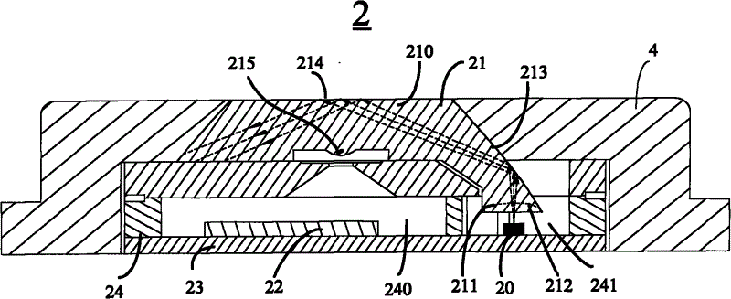
请参阅图2所示,为实施本实用新型的光学感应模块的结构示意图,其中该光学感应模块2包括光源20、透镜21、感光芯片22及电路板23。其中该光源20及感光芯片22均安装在电路板23上并与电路板23电性连接。在具体实施时,该光源20可以是相干光源(如激光)或者也可为非相干光源,较佳地该光源20是通过表面粘贴技术安装在电路板23上。而该电路板23可以是印刷电路板,也可以是柔性印刷电路板,并且该电路板23一端设有与使用该光学感应模块2的电路装置的电路板(未图示)相连接的接口,如金手指或电连接器等以与使用该光学感应模块2的电子装置的主电路板(未图示)电性连接。当然,此电路板23也可为使用该光学感应模块2的电子装置的电路板,即光源20与感光芯片22直接组设于该电子装置的电路板上。 Please refer to FIG. 2 , which is a structural diagram of an optical sensing module implementing the present invention, wherein the
透镜21设于感光芯片22及光源20上方,包括设置为一整体的照明光路(未标号)与成像光路(未标号),在结构上该透镜21包括一板状部210及凸出部211,该凸出部211与光源20相对的表面形成一凹球面212,并且光源20设置于凹球面212的中心,如此光源20发射的光线便可垂直于凹球面212入射至透镜21内,从而保持较高的光线透射率。同时,该透镜21的凸出部211在邻近凹球面212的另一表面设有照明光路的反射面213。另外,该透镜21的板状部210远离电路板23的表面并且与感光芯片22正对的位置设有供目标物体(如使用者手指)放置的操作区域214,而该透镜21的板状部210相对电路板23的表面并且与感光芯片22正对的位置设凸出设有一聚光透镜215。在实施时,该透镜21由透光材质制成,例如玻璃或透明的树脂,并且其折射率大于外部介质(如空气)的折射率。其中假如该透镜21的材质为透明树脂,其折射率为1.514,则空气与该透镜21表面的临界角为41.34度,如此只要对反射面213与光源20之间的高度及反射面213的曲率进行调 整,即可保证经反射面213反射的光线的入射角大于空气与透镜21表面的临界角,如此该光线在透镜21内部形成全反射,最后从透镜21的一侧射出,如此则没有光线从该透镜21表面折射出去,从而防止眩目,以提高使用的舒适度。再者,也可在该光学感应模块2外围再设置一盖体4,以形成一单独的元件模块,可以直接使用在手机、电子书等电子装置的外壳(未图示)上,并与该电子装置的主电路板(未图示)电性连接。 The
请参阅图3所示,为实施本实用新型的光学感应模块另一使用状态示意图,当目标物体3放置在透镜21的操作区域214上后,目标物体3的折射率比透镜21的折射率大(如目标物体可为不透明物体或手指),从而全反射条件被破坏,如此经反射面213反射的光线经目标物体3表面反射并经透镜21的聚光透镜215聚集后而照射到感光芯片22上,从而形成影像,之后与该感光芯片连接的数据处理单元(未图示)利用影像处理技术而实现对使用该光学感应模块的电子装置的屏幕光标进行控制或进行光学指纹识别。 Please refer to FIG. 3 , which is a schematic diagram of another usage state of the optical sensing module implementing the present utility model. When the
较佳地,在实施时为防止外部的光线及光源20的光线被散射至感光芯片22上,可在该感光芯片22外围设有一遮光壳体24,该遮光壳体24设有分别收容感光芯片22与光源20的第一与第二收容空间240、241,此第一与第二收容空间240、241相互隔离。当然,也可以在遮光壳体24与感光芯片22正对的壁面上设置一非球面透镜(为成像光路的一部分),经目标物体3表面反射后的光线经该非球面透镜聚集后照射在感光芯片22上,如此该透镜21上则不需设置聚光透镜215。或者,也可不需单独设置遮光壳体24,只需在透镜21邻近感光芯片22的侧面凸出设有二挡壁(未图示),该二挡壁邻近感光芯片22的表面设有防透光层(未图示),该感光芯片22容设于该二挡壁之间,如此也可防止外部的光线及光源20的光线被散射至感光芯片22上。 Preferably, in order to prevent external light and light from the
再者,在实施时,该光源20、感光芯片22及遮光壳体24可制造为一整体,即形成一单独的感应芯片,从而可直接焊接在电路板23上,之后再与透镜21形成一单独的模块。 Furthermore, during implementation, the
另外,上述的叙述中是假定目标物体3的折射率比透镜21的折射率大从而破坏全反射条件,当然也有一种情形是目标物体3的折射率小于透镜21的折射率,即透镜的折射率为n,透镜外的外部介质折射率为m,目标物体的折射率为k,并且透镜的折射率n大于外部介质折射率m,并且目标物体的折射率k小于透镜的折射率n,如此当目标物体未放置在操作区域上时,经反 射面反射的光线的入射角大于等于arcsin(m/n),即外部介质与该透镜21表面的临界角,如此经反射面反射的光线在透镜内形成全反射,而当目标物体放置在操作区域上后,由于目标物体的折射率k小于透镜的折射率n,因此目标物体与透镜的表面也会存在一个临界角,即arcsin(k/n),如果经反射面反射的光线的入射角大于此目标物体与透镜的表面的临界角,该光线也会在透镜内形成全反射而不能照射至感光芯片上形成感应图像,如此必须保证经反射面反射的光线的入射角要小于arcsin(k/n),即小于目标物体与该透镜表面的临界角,此时全反射条件被破坏,经反射面反射的光线经目标物体表面反射后才能照射到感光芯片上,即此种情形下需保证经反射面反射的光线的入射角大于等于arcsin(m/n)并小于等于arcsin(k/n),才能在目标物体未放置在操作区域上时,此光线形成全反射,而目标特体放置在操作区域上时,此光线才能被目标物体表面反射后照射到感光芯片上。 In addition, in the above-mentioned narration, it is assumed that the refractive index of the
当然,本实用新型也可以另外一种方式在电子装置上实施,该电子装置至少包括显示屏幕、主电路板及壳体,并且该电子装置还包括一光学感应模块,该光学感应模块包括一感应芯片及透镜,该感应芯片焊接于主电路板上,包括一光源、感光芯片及遮光壳体,该透镜设于感应芯片上方,该透镜包括一反射面与供目标物体放置的操作区域。与图2与图3所述的实施方式不同之处在于将光源、感光芯片及遮光壳体形成一独立的感应芯片,并且该感应芯片直接焊接在电子装置的主电路板上,之后再在该感应芯片上安装透镜等元件。 Of course, the utility model can also be implemented on an electronic device in another way, the electronic device at least includes a display screen, a main circuit board and a casing, and the electronic device also includes an optical sensing module, which includes a sensing Chip and lens, the sensing chip is welded on the main circuit board, including a light source, photosensitive chip and light-shielding housing, the lens is arranged above the sensing chip, and the lens includes a reflective surface and an operating area for placing a target object. The difference from the embodiment described in Fig. 2 and Fig. 3 is that the light source, the photosensitive chip and the light-shielding housing are formed into an independent sensing chip, and the sensing chip is directly welded on the main circuit board of the electronic device, and then on the Components such as lenses are installed on the sensing chip. the
与现有技术相比较,本实用新型通过令当目标物体未放置在操作区域上时,透镜的反射面反射的光线的入射角大于外部介质与该透镜表面的临界角,从而该光线在透镜内形成全反射,从而防止造成眩目以提高使用的舒适度,而目标物体放置在操作区域后,或者由于目标物体的折射率大于透镜的折射率从而全反射条件被破坏,或者当目标物体的折射率小于透镜的折射率时,由于经反射面反射的光线的入射角小于目标物体与该透镜表面的临界角从而全反射条件被破坏,由此经反射面反射的光线经目标物体表面反射后而照射到感光芯片上以形成图像。再者,由于直接在透镜表面设置供目标物体放置的操作区域,从而不需设置导航面板,并且反射面及聚光透镜等均整体设置在透镜上,从而利于降低该光学感应模块的整体高度,同时该光学感应模块不需其他单独或活动的元件,从而显得结构简单,易于制造,由此也可降低 该光学感应模块的制造成本。 Compared with the prior art, the utility model makes the incident angle of the light reflected by the reflective surface of the lens larger than the critical angle between the external medium and the lens surface when the target object is not placed on the operating area, so that the light is within the lens Form total reflection, so as to prevent glare and improve the comfort of use, and the target object is placed behind the operating area, or because the refractive index of the target object is greater than the refractive index of the lens, the total reflection condition is destroyed, or when the refraction of the target object When the index is less than the refractive index of the lens, since the incident angle of the light reflected by the reflective surface is smaller than the critical angle between the target object and the lens surface, the total reflection condition is destroyed, so the light reflected by the reflective surface is reflected by the surface of the target object. Illuminates onto a photosensitive chip to form an image. Furthermore, since the operation area for placing the target object is directly set on the surface of the lens, there is no need to set a navigation panel, and the reflective surface and the condensing lens are all set on the lens as a whole, thereby helping to reduce the overall height of the optical sensing module. At the same time, the optical sensing module does not need other independent or movable components, so it is simple in structure and easy to manufacture, thereby reducing the manufacturing cost of the optical sensing module. the
Claims (54)
Priority Applications (1)
| Application Number | Priority Date | Filing Date | Title |
|---|---|---|---|
| CN2010202793005U CN201867778U (en) | 2010-08-02 | 2010-08-02 | Electronic device and optical sensing module thereof |
Applications Claiming Priority (1)
| Application Number | Priority Date | Filing Date | Title |
|---|---|---|---|
| CN2010202793005U CN201867778U (en) | 2010-08-02 | 2010-08-02 | Electronic device and optical sensing module thereof |
Publications (1)
| Publication Number | Publication Date |
|---|---|
| CN201867778U true CN201867778U (en) | 2011-06-15 |
Family
ID=44138930
Family Applications (1)
| Application Number | Title | Priority Date | Filing Date |
|---|---|---|---|
| CN2010202793005U Expired - Fee Related CN201867778U (en) | 2010-08-02 | 2010-08-02 | Electronic device and optical sensing module thereof |
Country Status (1)
| Country | Link |
|---|---|
| CN (1) | CN201867778U (en) |
Cited By (6)
| Publication number | Priority date | Publication date | Assignee | Title |
|---|---|---|---|---|
| CN103049138A (en) * | 2011-10-12 | 2013-04-17 | 光宝新加坡有限公司 | Integrated optical module and finger scanning device thereof |
| CN106022323A (en) * | 2016-07-26 | 2016-10-12 | 昆山龙腾光电有限公司 | Finger identification system, finger identification method and fingerprint identification device |
| CN106684202A (en) * | 2017-01-04 | 2017-05-17 | 京东方科技集团股份有限公司 | Photosensitive assembly, fingerprint recognition panel and apparatus |
| CN107918450A (en) * | 2016-10-05 | 2018-04-17 | 三星电子株式会社 | Electronic device including biometric sensor |
| CN110087200A (en) * | 2012-01-07 | 2019-08-02 | 三星电子株式会社 | Electronic device and electronic equipment |
| US11409327B2 (en) | 2013-07-11 | 2022-08-09 | Samsung Electronics Co., Ltd. | User terminal device for displaying contents and methods thereof |
-
2010
- 2010-08-02 CN CN2010202793005U patent/CN201867778U/en not_active Expired - Fee Related
Cited By (12)
| Publication number | Priority date | Publication date | Assignee | Title |
|---|---|---|---|---|
| CN103049138A (en) * | 2011-10-12 | 2013-04-17 | 光宝新加坡有限公司 | Integrated optical module and finger scanning device thereof |
| CN110087200A (en) * | 2012-01-07 | 2019-08-02 | 三星电子株式会社 | Electronic device and electronic equipment |
| US11165896B2 (en) | 2012-01-07 | 2021-11-02 | Samsung Electronics Co., Ltd. | Method and apparatus for providing event of portable device having flexible display unit |
| US11409327B2 (en) | 2013-07-11 | 2022-08-09 | Samsung Electronics Co., Ltd. | User terminal device for displaying contents and methods thereof |
| US11675391B2 (en) | 2013-07-11 | 2023-06-13 | Samsung Electronics Co., Ltd. | User terminal device for displaying contents and methods thereof |
| US12066859B2 (en) | 2013-07-11 | 2024-08-20 | Samsung Electronics Co., Ltd. | User terminal device for displaying contents and methods thereof |
| CN106022323A (en) * | 2016-07-26 | 2016-10-12 | 昆山龙腾光电有限公司 | Finger identification system, finger identification method and fingerprint identification device |
| CN106022323B (en) * | 2016-07-26 | 2019-09-10 | 昆山龙腾光电有限公司 | Finger recognition system and finger identification method and fingerprint identification device |
| CN107918450A (en) * | 2016-10-05 | 2018-04-17 | 三星电子株式会社 | Electronic device including biometric sensor |
| CN107918450B (en) * | 2016-10-05 | 2023-08-04 | 三星电子株式会社 | Electronic device comprising a biometric sensor |
| CN106684202A (en) * | 2017-01-04 | 2017-05-17 | 京东方科技集团股份有限公司 | Photosensitive assembly, fingerprint recognition panel and apparatus |
| CN106684202B (en) * | 2017-01-04 | 2018-03-23 | 京东方科技集团股份有限公司 | A kind of photosensory assembly, fingerprint recognition panel and device |
Similar Documents
| Publication | Publication Date | Title |
|---|---|---|
| TWI635306B (en) | Optical apparatus | |
| CN201867778U (en) | Electronic device and optical sensing module thereof | |
| US8049726B2 (en) | Optical trace detecting module | |
| CN201465046U (en) | Thin Optical Indicator Module | |
| CN102063223A (en) | Pointing device and electronic apparatus | |
| US10515253B2 (en) | Optical fingerprint sensor | |
| CN105893932A (en) | Optical device | |
| TWI433009B (en) | Optical touch apparatus | |
| CN104423579A (en) | Electronic Device Having Proximity Touch Function And Control Method Thereof | |
| CN106650561A (en) | Fingerprint image capturing device and fingerprint image capturing module thereof | |
| CN105072998A (en) | Palm vein image capture device | |
| TW200947275A (en) | Optical trace detection module | |
| CN108564023A (en) | Fingerprint identification device and display equipment | |
| CN109564338A (en) | Lens group, fingerprint identification device and electronic equipment | |
| KR101697131B1 (en) | Interactive display device | |
| CN102346574A (en) | Electronic device and optical sensing module thereof | |
| WO2006092665A2 (en) | Continuous base beneath optical sensor and optical homodyning system | |
| CN102375621A (en) | Optical navigation device | |
| CN102486702A (en) | Reflective optical detection device and electronic equipment | |
| CN102200864B (en) | Optical touch device | |
| CN201522712U (en) | Image capturing module capable of electrically connecting two circuit substrates | |
| CN208953768U (en) | Lens group, fingerprint identification device and electronic equipment | |
| CN101825797A (en) | Photo induction touch-control liquid crystal display device | |
| CN108683756B (en) | Fingerprint identification assembly, display device and electronic device | |
| CN201828885U (en) | Thin-type optical indicating device |
Legal Events
| Date | Code | Title | Description |
|---|---|---|---|
| C14 | Grant of patent or utility model | ||
| GR01 | Patent grant | ||
| DD01 | Delivery of document by public notice |
Addressee: Gao Yong Document name: Notification to Pay the Fees |
|
| DD01 | Delivery of document by public notice |
Addressee: Gao Yong Document name: Notification of Termination of Patent Right |
|
| C17 | Cessation of patent right | ||
| CF01 | Termination of patent right due to non-payment of annual fee |
Granted publication date: 20110615 Termination date: 20130802 |