CN1952764B - Thin film transistor array panel and liquid crystal display - Google Patents
Thin film transistor array panel and liquid crystal display Download PDFInfo
- Publication number
- CN1952764B CN1952764B CN2006101359515A CN200610135951A CN1952764B CN 1952764 B CN1952764 B CN 1952764B CN 2006101359515 A CN2006101359515 A CN 2006101359515A CN 200610135951 A CN200610135951 A CN 200610135951A CN 1952764 B CN1952764 B CN 1952764B
- Authority
- CN
- China
- Prior art keywords
- pixel
- electrode
- gate
- line
- film transistor
- Prior art date
- Legal status (The legal status is an assumption and is not a legal conclusion. Google has not performed a legal analysis and makes no representation as to the accuracy of the status listed.)
- Expired - Fee Related
Links
Images


Classifications
-
- G—PHYSICS
- G02—OPTICS
- G02F—OPTICAL DEVICES OR ARRANGEMENTS FOR THE CONTROL OF LIGHT BY MODIFICATION OF THE OPTICAL PROPERTIES OF THE MEDIA OF THE ELEMENTS INVOLVED THEREIN; NON-LINEAR OPTICS; FREQUENCY-CHANGING OF LIGHT; OPTICAL LOGIC ELEMENTS; OPTICAL ANALOGUE/DIGITAL CONVERTERS
- G02F1/00—Devices or arrangements for the control of the intensity, colour, phase, polarisation or direction of light arriving from an independent light source, e.g. switching, gating or modulating; Non-linear optics
- G02F1/01—Devices or arrangements for the control of the intensity, colour, phase, polarisation or direction of light arriving from an independent light source, e.g. switching, gating or modulating; Non-linear optics for the control of the intensity, phase, polarisation or colour
- G02F1/13—Devices or arrangements for the control of the intensity, colour, phase, polarisation or direction of light arriving from an independent light source, e.g. switching, gating or modulating; Non-linear optics for the control of the intensity, phase, polarisation or colour based on liquid crystals, e.g. single liquid crystal display cells
- G02F1/133—Constructional arrangements; Operation of liquid crystal cells; Circuit arrangements
- G02F1/1333—Constructional arrangements; Manufacturing methods
- G02F1/1343—Electrodes
-
- G—PHYSICS
- G02—OPTICS
- G02F—OPTICAL DEVICES OR ARRANGEMENTS FOR THE CONTROL OF LIGHT BY MODIFICATION OF THE OPTICAL PROPERTIES OF THE MEDIA OF THE ELEMENTS INVOLVED THEREIN; NON-LINEAR OPTICS; FREQUENCY-CHANGING OF LIGHT; OPTICAL LOGIC ELEMENTS; OPTICAL ANALOGUE/DIGITAL CONVERTERS
- G02F1/00—Devices or arrangements for the control of the intensity, colour, phase, polarisation or direction of light arriving from an independent light source, e.g. switching, gating or modulating; Non-linear optics
- G02F1/01—Devices or arrangements for the control of the intensity, colour, phase, polarisation or direction of light arriving from an independent light source, e.g. switching, gating or modulating; Non-linear optics for the control of the intensity, phase, polarisation or colour
- G02F1/13—Devices or arrangements for the control of the intensity, colour, phase, polarisation or direction of light arriving from an independent light source, e.g. switching, gating or modulating; Non-linear optics for the control of the intensity, phase, polarisation or colour based on liquid crystals, e.g. single liquid crystal display cells
- G02F1/133—Constructional arrangements; Operation of liquid crystal cells; Circuit arrangements
- G02F1/136—Liquid crystal cells structurally associated with a semi-conducting layer or substrate, e.g. cells forming part of an integrated circuit
- G02F1/1362—Active matrix addressed cells
- G02F1/136286—Wiring, e.g. gate line, drain line
-
- G—PHYSICS
- G09—EDUCATION; CRYPTOGRAPHY; DISPLAY; ADVERTISING; SEALS
- G09G—ARRANGEMENTS OR CIRCUITS FOR CONTROL OF INDICATING DEVICES USING STATIC MEANS TO PRESENT VARIABLE INFORMATION
- G09G3/00—Control arrangements or circuits, of interest only in connection with visual indicators other than cathode-ray tubes
- G09G3/20—Control arrangements or circuits, of interest only in connection with visual indicators other than cathode-ray tubes for presentation of an assembly of a number of characters, e.g. a page, by composing the assembly by combination of individual elements arranged in a matrix no fixed position being assigned to or needed to be assigned to the individual characters or partial characters
- G09G3/34—Control arrangements or circuits, of interest only in connection with visual indicators other than cathode-ray tubes for presentation of an assembly of a number of characters, e.g. a page, by composing the assembly by combination of individual elements arranged in a matrix no fixed position being assigned to or needed to be assigned to the individual characters or partial characters by control of light from an independent source
- G09G3/36—Control arrangements or circuits, of interest only in connection with visual indicators other than cathode-ray tubes for presentation of an assembly of a number of characters, e.g. a page, by composing the assembly by combination of individual elements arranged in a matrix no fixed position being assigned to or needed to be assigned to the individual characters or partial characters by control of light from an independent source using liquid crystals
- G09G3/3611—Control of matrices with row and column drivers
- G09G3/3648—Control of matrices with row and column drivers using an active matrix
- G09G3/3659—Control of matrices with row and column drivers using an active matrix the addressing of the pixel involving the control of two or more scan electrodes or two or more data electrodes, e.g. pixel voltage dependant on signal of two data electrodes
-
- G—PHYSICS
- G09—EDUCATION; CRYPTOGRAPHY; DISPLAY; ADVERTISING; SEALS
- G09G—ARRANGEMENTS OR CIRCUITS FOR CONTROL OF INDICATING DEVICES USING STATIC MEANS TO PRESENT VARIABLE INFORMATION
- G09G2310/00—Command of the display device
- G09G2310/02—Addressing, scanning or driving the display screen or processing steps related thereto
- G09G2310/0202—Addressing of scan or signal lines
- G09G2310/0205—Simultaneous scanning of several lines in flat panels
-
- G—PHYSICS
- G09—EDUCATION; CRYPTOGRAPHY; DISPLAY; ADVERTISING; SEALS
- G09G—ARRANGEMENTS OR CIRCUITS FOR CONTROL OF INDICATING DEVICES USING STATIC MEANS TO PRESENT VARIABLE INFORMATION
- G09G3/00—Control arrangements or circuits, of interest only in connection with visual indicators other than cathode-ray tubes
- G09G3/20—Control arrangements or circuits, of interest only in connection with visual indicators other than cathode-ray tubes for presentation of an assembly of a number of characters, e.g. a page, by composing the assembly by combination of individual elements arranged in a matrix no fixed position being assigned to or needed to be assigned to the individual characters or partial characters
- G09G3/34—Control arrangements or circuits, of interest only in connection with visual indicators other than cathode-ray tubes for presentation of an assembly of a number of characters, e.g. a page, by composing the assembly by combination of individual elements arranged in a matrix no fixed position being assigned to or needed to be assigned to the individual characters or partial characters by control of light from an independent source
- G09G3/36—Control arrangements or circuits, of interest only in connection with visual indicators other than cathode-ray tubes for presentation of an assembly of a number of characters, e.g. a page, by composing the assembly by combination of individual elements arranged in a matrix no fixed position being assigned to or needed to be assigned to the individual characters or partial characters by control of light from an independent source using liquid crystals
- G09G3/3607—Control arrangements or circuits, of interest only in connection with visual indicators other than cathode-ray tubes for presentation of an assembly of a number of characters, e.g. a page, by composing the assembly by combination of individual elements arranged in a matrix no fixed position being assigned to or needed to be assigned to the individual characters or partial characters by control of light from an independent source using liquid crystals for displaying colours or for displaying grey scales with a specific pixel layout, e.g. using sub-pixels
-
- G—PHYSICS
- G09—EDUCATION; CRYPTOGRAPHY; DISPLAY; ADVERTISING; SEALS
- G09G—ARRANGEMENTS OR CIRCUITS FOR CONTROL OF INDICATING DEVICES USING STATIC MEANS TO PRESENT VARIABLE INFORMATION
- G09G3/00—Control arrangements or circuits, of interest only in connection with visual indicators other than cathode-ray tubes
- G09G3/20—Control arrangements or circuits, of interest only in connection with visual indicators other than cathode-ray tubes for presentation of an assembly of a number of characters, e.g. a page, by composing the assembly by combination of individual elements arranged in a matrix no fixed position being assigned to or needed to be assigned to the individual characters or partial characters
- G09G3/34—Control arrangements or circuits, of interest only in connection with visual indicators other than cathode-ray tubes for presentation of an assembly of a number of characters, e.g. a page, by composing the assembly by combination of individual elements arranged in a matrix no fixed position being assigned to or needed to be assigned to the individual characters or partial characters by control of light from an independent source
- G09G3/36—Control arrangements or circuits, of interest only in connection with visual indicators other than cathode-ray tubes for presentation of an assembly of a number of characters, e.g. a page, by composing the assembly by combination of individual elements arranged in a matrix no fixed position being assigned to or needed to be assigned to the individual characters or partial characters by control of light from an independent source using liquid crystals
- G09G3/3611—Control of matrices with row and column drivers
- G09G3/3614—Control of polarity reversal in general
Landscapes
- Physics & Mathematics (AREA)
- Nonlinear Science (AREA)
- Engineering & Computer Science (AREA)
- Crystallography & Structural Chemistry (AREA)
- General Physics & Mathematics (AREA)
- Chemical & Material Sciences (AREA)
- Mathematical Physics (AREA)
- Optics & Photonics (AREA)
- Computer Hardware Design (AREA)
- Theoretical Computer Science (AREA)
- Microelectronics & Electronic Packaging (AREA)
- Liquid Crystal (AREA)
- Liquid Crystal Display Device Control (AREA)
- Control Of Indicators Other Than Cathode Ray Tubes (AREA)
Abstract
本发明涉及一种薄膜晶体管阵列板,包括:多个像素,包括以矩阵布置的像素电极以及连接到该像素电极的开关元件;连接到该开关元件的第一和第二栅极线,沿行方向延伸且对应于一行像素电极;以及连接到该开关元件的第一和第二数据线,沿列方向延伸且对应于三个像素列。在该薄膜晶体管阵列板中,当所述三个像素列被称为第一至第三像素列时,在该第一和第二像素列中的所述像素电极经所述开关元件连接到该第一数据线,且该第三像素列中的所述像素电极经该开关元件连接到该第二数据线。
The invention relates to a thin film transistor array panel, comprising: a plurality of pixels, including pixel electrodes arranged in a matrix and switching elements connected to the pixel electrodes; first and second gate lines connected to the switching elements along the row extending in a direction and corresponding to one row of pixel electrodes; and first and second data lines connected to the switching element extending in a column direction and corresponding to three pixel columns. In the thin film transistor array panel, when the three pixel columns are referred to as first to third pixel columns, the pixel electrodes in the first and second pixel columns are connected to the a first data line, and the pixel electrodes in the third pixel column are connected to the second data line through the switch element.
Description
技术领域technical field
本发明涉及具有薄膜晶体管阵列板的液晶显示器。The present invention relates to a liquid crystal display having a thin film transistor array panel.
背景技术Background technique
液晶显示器包括两个显示板,一个具有像素电极,另一个具有公共电极,具有介电各向异性的液晶层在他们之间。像素电极以矩阵布置,并连接到开关元件例如薄膜晶体管(TFT)。数据电压依次施加到像素电极的行。公共电极被提供以公共电压。像素电极、公共电极和各向异性介电液晶层形成液晶电容器结构。液晶电容器和与其连接的开关元件构成像素单元。A liquid crystal display includes two display panels, one having pixel electrodes and the other having a common electrode, with a liquid crystal layer having dielectric anisotropy between them. The pixel electrodes are arranged in a matrix, and are connected to switching elements such as thin film transistors (TFTs). The data voltages are sequentially applied to rows of pixel electrodes. The common electrode is supplied with a common voltage. The pixel electrode, the common electrode and the anisotropic dielectric liquid crystal layer form a liquid crystal capacitor structure. A liquid crystal capacitor and a switching element connected thereto constitute a pixel unit.
当电压施加到液晶显示器的两个电极时,在液晶层中产生电场。电场强度控制光穿过液晶层的透射率,由此显示所需图像。为了防止显示的衰减,每一帧、每一列或每个像素周期地反转数据电压相对于公共电压的极性。When a voltage is applied to the two electrodes of the liquid crystal display, an electric field is generated in the liquid crystal layer. The strength of the electric field controls the transmittance of light through the liquid crystal layer, thereby displaying a desired image. In order to prevent degradation of the display, the polarity of the data voltage with respect to the common voltage is periodically reversed every frame, every column, or every pixel.
液晶显示器包括传递栅极信号以控制开关元件的栅极线、传递将被施加到电场生成电极的数据电压的数据线、产生栅极信号的栅极驱动器、以及产生数据电压的数据驱动器。一般地,栅极驱动器和数据驱动器由多个驱动器IC芯片构成。The liquid crystal display includes gate lines transmitting gate signals to control switching elements, data lines transmitting data voltages to be applied to electric field generating electrodes, a gate driver generating gate signals, and a data driver generating data voltages. Generally, a gate driver and a data driver are composed of a plurality of driver IC chips.
发明内容Contents of the invention
为了减少驱动器IC芯片的数量并由此降低制造成本,减少数据驱动器IC芯片的数量尤为重要,因为数据驱动器IC芯片比栅极驱动电路芯片更贵。In order to reduce the number of driver IC chips and thereby reduce manufacturing costs, it is particularly important to reduce the number of data driver IC chips because data driver IC chips are more expensive than gate drive circuit chips.
根据本发明一实施例,对每三个像素列设置两条数据线,由此减少为数据线供给信号的数据驱动芯片的数量。虽然栅极线的数量翻倍,但因为栅极驱动芯片不贵,所以栅极驱动芯片数量的增加对制造成本没有显著影响。另外,由于为栅极线供给驱动信号的栅极驱动电路执行非常简单的功能,所以栅极驱动电路可以通过利用薄膜晶体管形成工艺集成到衬底中,由此减少栅极驱动芯片的数量。According to an embodiment of the present invention, two data lines are provided for every three pixel columns, thereby reducing the number of data driving chips for supplying signals to the data lines. Although the number of gate lines is doubled, the increase in the number of gate drive chips does not have a significant impact on manufacturing cost because the gate drive chips are not expensive. In addition, since a gate driving circuit supplying a driving signal to a gate line performs a very simple function, the gate driving circuit can be integrated into a substrate by using a thin film transistor forming process, thereby reducing the number of gate driving chips.
薄膜晶体管阵列板包括对应于一行像素电极在行方向上延伸连接到开关元件的第一和第二栅极线、以及对应于三个像素列在列方向上延伸连接到开关元件的第一和第二数据线。关于三个像素列的组,第一和第二像素列中的像素电极经开关元件连接到第一数据线,第三像素列中的像素电极经开关元件连接到第二数据线。The thin film transistor array board includes first and second gate lines corresponding to one row of pixel electrodes extending in the row direction and connected to the switching elements, and corresponding to three pixel columns extending in the column direction and connected to the switching elements first and second gate lines. data line. Regarding the group of three pixel columns, the pixel electrodes in the first and second pixel columns are connected to the first data line via the switching element, and the pixel electrodes in the third pixel column are connected to the second data line via the switching element.
薄膜晶体管阵列板包括向第一和第二栅极线供给栅极导通或栅极截止电压的栅极驱动电路。此外,向第一栅极线施加栅极导通电压时,栅极驱动电路向第二栅极线施加栅极导通电压。The thin film transistor array panel includes a gate driving circuit supplying a gate-on or gate-off voltage to the first and second gate lines. In addition, when the gate-on voltage is applied to the first gate line, the gate driving circuit applies the gate-on voltage to the second gate line.
薄膜晶体管阵列板还包括数据驱动电路,其向第一和第二数据线提供图像信号,并且数据驱动电路可提供两点反转驱动信号。The thin film transistor array panel also includes a data driving circuit that provides image signals to the first and second data lines, and the data driving circuit can provide two-dot inversion driving signals.
薄膜晶体管阵列板还可包括与第一至第三像素列对应的冗余数据线。冗余数据线可以连接到第一数据线,可以对冗余数据线施加预定电压。The thin film transistor array panel may further include redundant data lines corresponding to the first to third pixel columns. A redundant data line may be connected to the first data line, and a predetermined voltage may be applied to the redundant data line.
薄膜晶体管阵列板还可包括:连接部分,其每个把第一数据线连接到第二数据线;引线部分,其把第一和第二数据线连接到数据驱动电路;以及连接元件,其把引线部分连接到连接部分。至少部分第三数据线可以在引线部分与将被连接到数据驱动电路的连接部分之间通过。The thin film transistor array panel may further include: connection parts each connecting the first data line to the second data line; lead parts connecting the first and second data lines to the data driving circuit; and connection elements connecting the first data line to the second data line; The lead part is connected to the connection part. At least part of the third data line may pass between the lead part and the connection part to be connected to the data driving circuit.
当一个像素列组包括顺序布置的第一至第三像素列时,偶数像素列组的第三数据线可以在引线部分与将被连接到数据驱动电路的连接部分之间通过,并且奇数像素列组的第三数据线可以不在引线部分与连接部分之间通过。When a pixel column group includes the first to third pixel columns arranged in sequence, the third data line of the even pixel column group can pass between the lead part and the connection part to be connected to the data driving circuit, and the odd pixel column The third data line of the group may not pass between the lead part and the connection part.
每个像素电极可包括沿不同方向倾斜的两个平行四边形电极片,两个电极片的斜边可以彼此相交,从而形成一对曲边。Each pixel electrode may include two parallelogram-shaped electrode pieces inclined in different directions, and the oblique sides of the two electrode pieces may intersect each other to form a pair of curved sides.
当用作一个像素电极的该对子像素电极被称作第一和第二子像素电极时,第一子像素电极可以与第一存储电极线交迭,第二子像素电极可以与第二存储电极线交迭。不同的电压可以施加到第一存储电极线和第二存储电极线。When the pair of subpixel electrodes used as one pixel electrode are referred to as first and second subpixel electrodes, the first subpixel electrode may overlap with the first storage electrode line, and the second subpixel electrode may overlap with the second storage electrode line. The electrode lines overlap. Different voltages may be applied to the first storage electrode line and the second storage electrode line.
该薄膜晶体管阵列板还可包括与第二子像素电极交迭的第三存储电极线。此外,不同的电压可以施加到第一存储电极线和第二存储电极线,相同的电压可以施加到第二存储电极线和第三存储电极线。The thin film transistor array panel may further include a third storage electrode line overlapping the second subpixel electrode. In addition, different voltages may be applied to the first storage electrode line and the second storage electrode line, and the same voltage may be applied to the second storage electrode line and the third storage electrode line.
每个开关元件可包括连接到第一栅极线或第二栅极线的栅电极、连接到第一至第三数据线的任一个的源电极、以及在栅电极上与源电极相对且具有扩展部分的漏电极。在第一和第三像素列中漏电极的扩展部分可以与第一存储电极线交迭,在第二像素列中漏电极的扩展部分可以与第二存储电极线交迭。每个子像素电极可包括沿不同方向倾斜的两个平行四边形电极片,两个电极片的斜边可以彼此相交,从而形成一对曲边。Each switching element may include a gate electrode connected to the first gate line or the second gate line, a source electrode connected to any one of the first to third data lines, and a gate electrode opposite to the source electrode and having The drain electrode of the extension. The extended portion of the drain electrode may overlap the first storage electrode line in the first and third pixel columns, and the extended portion of the drain electrode may overlap the second storage electrode line in the second pixel column. Each sub-pixel electrode may include two parallelogram-shaped electrode pieces inclined in different directions, and oblique sides of the two electrode pieces may intersect each other to form a pair of curved sides.
附图说明Description of drawings
通过下面结合附图的详细描述,本发明的前述目的和特点将变得更加清晰,其中:Through the following detailed description in conjunction with the accompanying drawings, the aforementioned purposes and features of the present invention will become clearer, wherein:
图1是示出根据本发明一示例性实施例的液晶显示器的框图;1 is a block diagram illustrating a liquid crystal display according to an exemplary embodiment of the present invention;
图2是根据本发明一示例性实施例的液晶显示器的一个像素的等效电路图;2 is an equivalent circuit diagram of a pixel of a liquid crystal display according to an exemplary embodiment of the present invention;
图3是示出根据本发明一示例性实施例的薄膜晶体管阵列板的电路图;3 is a circuit diagram illustrating a thin film transistor array panel according to an exemplary embodiment of the present invention;
图4是根据本发明一示例性实施例的薄膜晶体管阵列板的布局图;4 is a layout diagram of a thin film transistor array panel according to an exemplary embodiment of the present invention;
图5是薄膜晶体管阵列板沿图4的V-V′线截取的剖视图;Fig. 5 is a cross-sectional view of the thin film transistor array board taken along the line V-V' of Fig. 4;
图6是薄膜晶体管阵列板沿图4的VI-VI′线截取的剖视图;Fig. 6 is a cross-sectional view of the thin film transistor array board taken along line VI-VI' of Fig. 4;
图7A和7B是时间图(timing chart),示出根据本发明一示例性实施例的液晶显示器的驱动电压;7A and 7B are timing charts showing driving voltages of a liquid crystal display according to an exemplary embodiment of the present invention;
图8-12以及图14和15是布局图,示出根据本发明另一示例性实施例的薄膜晶体管阵列板的布局图;8-12 and FIGS. 14 and 15 are layout diagrams showing a layout diagram of a thin film transistor array panel according to another exemplary embodiment of the present invention;
图13是沿图12的XIII-XIII线截取的剖视图。Fig. 13 is a sectional view taken along line XIII-XIII of Fig. 12 .
具体实施方式Detailed ways
下面将结合附图对本发明作全面的描述,附图中示出了本发明的优选实施例。为了清楚起见,附图中夸大了层、膜、板、区的厚度。整个说明书中用相似的附图标记表示相似的元件。应理解,当诸如层、膜、区或衬底的元件被称为在另一元件“上”时,它可以直接位于另一元件上,或者也可以存在中间元件。相反,当一个元件被称为“直接”在另一元件“上”时,则不存在中间元件。The present invention will now be fully described with reference to the accompanying drawings, in which preferred embodiments of the invention are shown. In the drawings, the thickness of layers, films, panels and regions are exaggerated for clarity. Like reference numerals are used to refer to like elements throughout the specification. It will be understood that when an element such as a layer, film, region, or substrate is referred to as being "on" another element, it can be directly on the other element or intervening elements may also be present. In contrast, when an element is referred to as being "directly on" another element, there are no intervening elements present.
如图1所示,根据本发明一示例性实施例的液晶显示器包括液晶板组件300、连接到液晶板组件300的栅极驱动器400和数据驱动器500、连接到数据驱动器500的灰度电压发生器800、以及用于控制上述部件的信号控制器600。在等效电路图中,液晶板组件300连接到多个显示信号线G1-1-Gn-2以及D1-1-Dm-2,并且包括基本以矩阵布置的多个像素。As shown in FIG. 1, a liquid crystal display according to an exemplary embodiment of the present invention includes a liquid crystal panel assembly 300, a gate driver 400 and a data driver 500 connected to the liquid crystal panel assembly 300, and a grayscale voltage generator connected to the data driver 500. 800, and a signal controller 600 for controlling the above components. In the equivalent circuit diagram, the liquid crystal panel assembly 300 is connected to a plurality of display signal lines G 1-1 -G n-2 and D 1-1 -D m-2 , and includes a plurality of pixels substantially arranged in a matrix.
显示信号线G1-1-Gn-2以及D1-1-Dm-2包括用于传递栅极信号(称作“扫描信号”)的多个栅极线G1-1-Gn-2和用于传递数据信号的多个数据线D1-1-Dm-2。栅极线G1-1-Gn-2基本在行方向上延伸,从而彼此平行,数据线D1-1-Dm-2基本在列方向上延伸,从而彼此平行。The display signal lines G 1-1 -G n-2 and D 1-1 -D m-2 include a plurality of gate lines G 1-1 -G n for transmitting gate signals (referred to as "scanning signals") -2 and a plurality of data lines D 1-1 -D m-2 for transmitting data signals. The gate lines G 1-1 -G n-2 extend substantially in the row direction so as to be parallel to each other, and the data lines D 1-1 -D m-2 extend substantially in the column direction so as to be parallel to each other.
每个像素包括连接到显示信号线G1-1-Gn-2以及D1-1-Dm-2之一的开关元件Q、连接到开关元件Q的液晶电容器CLC、以及存储电容器CST。如果需要的话,可以省去存储电容器CST。Each pixel includes a switching element Q connected to one of the display signal lines G 1-1 -G n-2 and D 1-1 -D m-2 , a liquid crystal capacitor C LC connected to the switching element Q, and a storage capacitor C ST . The storage capacitor C ST can be omitted if desired.
开关元件Q是三端子元件,例如薄膜晶体管,且设置在下板100上。开关元件Q的控制端子连接到栅极线G1-1-Gn-2,其输入端子连接到数据线D1-1-Dm-2,其输出端子连接到液晶电容器CLC和存储电容器CST。The switching element Q is a three-terminal element such as a thin film transistor, and is provided on the
液晶电容器CLC有两个端子,下板100的像素电极191和上板200的公共电极270,液晶层3在两电极之间作为电介质材料。像素电极191连接到开关元件Q,公共电极270形成在上板200的整个表面上并被提供以公共电压Vcom。与图2所示的结构不同,公共电极270可设置在下板100上,在该情况下,两电极191和270中的至少一个可形成为线形或条形。The liquid crystal capacitor C LC has two terminals, the
充当液晶电容器CLC的辅助元件的存储电容器CST包括设置在下板100上的信号线(未示出)、像素电极191和置于其间的绝缘体。对信号线施加预定电压例如公共电压Vcom。供选地,存储电容器CST可以是像素电极191、绝缘体和形成在绝缘体上的前栅极线的叠置结构。The storage capacitor C ST serving as an auxiliary element of the liquid crystal capacitor C LC includes a signal line (not shown) disposed on the
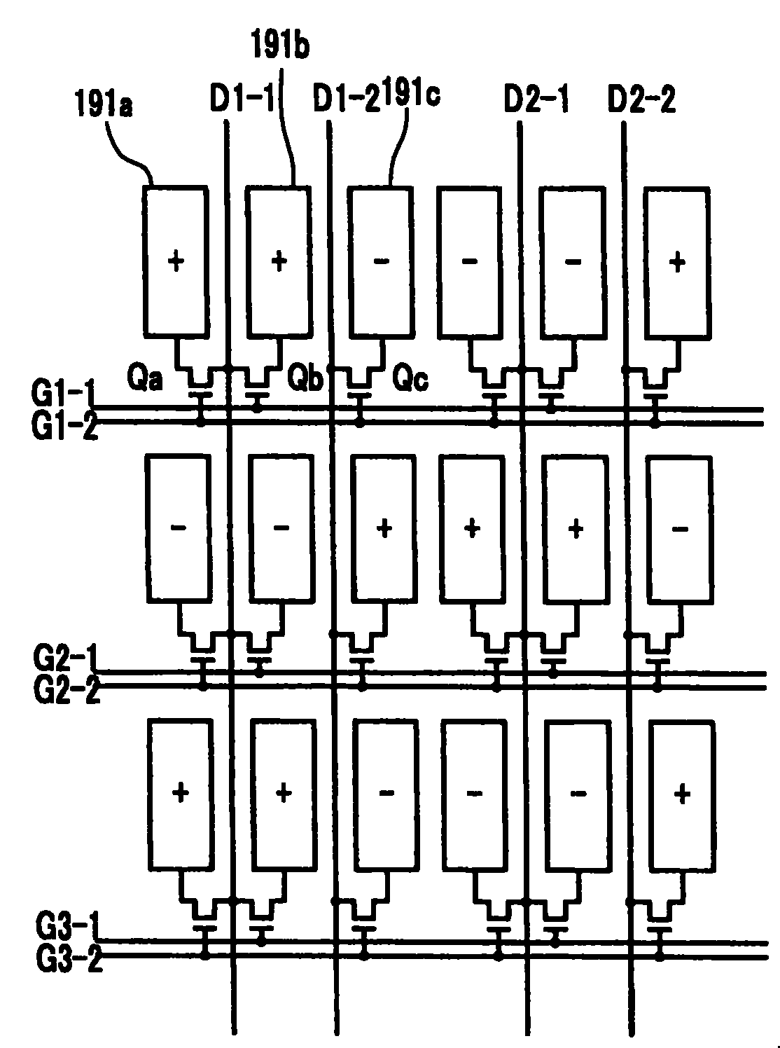
如图3所示,每对栅极线G1-n和G1-(n+1)(n是自然数)依次设置在像素191的对应行之下。每条数据线D1-1、D1-2、D2-1、D2-2等设置在相邻的两列像素之间。假设三个像素列属于一个像素列组,则数据线的对D1-1和D1-2、D2-1和D2-2等被包括在一个像素列组中,从而没有数据线设置在一个像素列组和另一像素列组之间。像素电极191、栅极线G1-1-Gn-2和数据线D1-1-Dm-2将在后面详细描述。As shown in FIG. 3 , each pair of gate lines G 1-n and G 1-(n+1) (n is a natural number) is sequentially disposed under the corresponding row of
多对栅极线G1-1-Gn-2设置在像素电极191a、191b和191c下面,并且经布置在像素电极191a、191b和191c下面的开关元件Qa、Qb和Qc连接到像素电极191a、191b和191c。在此结构中,当一对栅极线Gn-1和Gn-2的上栅极线称作第一栅极线Gn-1,其下栅极线称作第二栅极线Gn-2时,第一栅极线Gn-1连接到像素列组的第一像素列中的像素电极191b,第二栅极线Gn-2连接到像素列组的第一和第三像素列中的第一和第三像素电极191a和191c。A plurality of pairs of gate lines G 1-1 -G n-2 are disposed under the
设置在像素电极191a、191b和191c之间的多对数据线D1-1-Dm-2经布置在像素电极191a、191b和191c下面的开关元件Qa、Qb和Qc连接到对应的像素电极191a、191b和191c。在此结构中,当一像素列组中两条数据线的左数据线称作第一数据线Dm-1且其右数据线称作第二数据线Dm-2时,第一数据线Dm-1连接到设置在第一数据线Dm-1两侧的第一和第二像素列中的像素电极191a和191b,并且第二数据线Dm-2连接到设置在第二数据线Dm-2右侧的第三像素列中的像素电极191c。Pairs of data lines D1-1 - Dm-2 disposed between the
即,第一像素列中的开关元件Qa连接到第二栅极线Gn-2、第一数据线Dm-1以及第一像素列中的像素电极191a,第二像素列中的开关元件Qb连接到第一栅极线Gn-1、第一数据线Dm-1以及第二像素列中的像素电极191b。此外,第三像素列中的开关元件Qc连接到第二栅极线Gn-2、第二数据线Dm-2和第三像素列中的像素电极191c。That is, the switching element Qa in the first pixel column is connected to the second gate line Gn -2 , the first data line Dm -1 , and the
为了进行彩色显示,每个像素具体显示一种基色(空间划分),或者像素随时间交替显示基色(时间划分),这使基色被空间或时间合成,由此显示所需颜色。作为空间划分的示例,图2示出每个像素在与像素电极191对应的区域中具有用于显示红、绿和蓝之一的滤色片230。与图2所示的结构不同,滤色片230可设置在下板100的像素电极191之上或之下。For color display, each pixel specifically displays a primary color (spatial division), or pixels alternately display primary colors over time (temporal division), which allows the primary colors to be spatially or temporally synthesized, thereby displaying a desired color. As an example of space division, FIG. 2 shows that each pixel has a
在图3中,优选一像素列组的第一至第三像素列分别为红、绿和蓝像素列。供选地,第一至第三像素列可以由红、绿和蓝像素列的不同组合形成。In FIG. 3 , preferably, the first to third pixel columns of a pixel column group are red, green and blue pixel columns, respectively. Alternatively, the first to third pixel columns may be formed of different combinations of red, green and blue pixel columns.
用于使光偏振的偏振片(未示出)安装到液晶板组件300的两个显示板100和200中至少一个的外表面。A polarizing plate (not shown) for polarizing light is mounted to an outer surface of at least one of the two
接下来将参考图4-6详细描述液晶板组件300的薄膜晶体管阵列板100的结构。图4是布局图,示出根据本发明一示例性实施例的薄膜晶体管阵列板,图5是薄膜晶体管阵列板的沿图4的V-V′线截取的剖视图,图6是薄膜晶体管阵列板的沿图4的VI-VI′线截取的剖视图。Next, the structure of the thin film
如上所述,根据本发明一示例性实施例的液晶显示器包括薄膜晶体管阵列板100、与薄膜晶体管阵列板100相对的公共电极板200、以及置于薄膜晶体管阵列板100和公共电极板200之间的液晶层3。As described above, a liquid crystal display according to an exemplary embodiment of the present invention includes a thin film
接下来将详细描述薄膜晶体管阵列板100。多对栅极线121和122以及防漏光元件126形成在由例如透明玻璃制成的绝缘基板110上。Next, the thin film
成对的栅极线121和122在水平方向上延伸。每条栅极线121的部分向上突出,从而形成栅电极124b,并且每条栅极线122的部分向下突出,从而形成栅电极124a和124c。栅极线121连接到集成于基板110中的栅极驱动电路(未示出),栅极线122的一端129具有较大的宽度,用于与其它层或外部器件的连接。The paired
在彼此相邻的两对栅极线121和122之间沿垂直方向纵向地形成防漏光元件126,且在每个像素的像素区的两侧设置两个防漏光元件126。A light
栅极线121和122以及防漏光元件126可以由例如诸如铝(Al)或铝合金的铝基金属材料、诸如银(Ag)或银合金的银基金属材料、诸如铜(Cu)或铜合金的铜基金属材料、诸如钼(Mo)或钼合金的钼基金属材料、铬(Cr)、钽(Ta)或钛(Ti)形成。供选地,栅极线121和122以及防漏光元件126可包括具有不同物理属性的两层膜,即下层(未示出)和上层(未示出)。上层可以由低电阻金属材料例如,诸如铝(Al)或铝合金的铝基金属材料、诸如银(Ag)或银合金的银基金属材料、诸如铜(Cu)或铜合金的铜基金属材料形成,以减小栅极线121和122以及防漏光元件126中的信号延迟或电压降。相反,下层可以由与形成上层的材料不同的材料形成,即可以用尤其与ITO(氧化铟锡)和IZO(氧化铟锌)具有良好接触特性的材料例如铬、钼(Mo)、钼合金、钽(Ta)或钛(Ti)形成。铬/铝-钕(Nd)合金可以作为下层与上层结合的示例。The gate lines 121 and 122 and the light
栅极线121和122以及防漏光元件126的侧表面相对于基板110的表面倾斜,优选倾斜30°-80°角。Side surfaces of the
由例如氮化硅(SiNx)形成的栅极绝缘层140形成在栅极线121和122以及防漏光元件126上。A
由氢化非晶硅(缩写为a-Si)或多晶硅形成的多个半导体岛154a、154b和154c例如形成在栅极绝缘层140上。半导体岛154a、154b和154c分别位于栅电极124a、124b和124c之上,两半导体154a和154b之间的连接部分覆盖栅极线121和122。半导体154c延伸从而覆盖两条栅极线121和122。A plurality of
在半导体154a、154b和154c上形成由含硅化物或高浓度掺杂的n型杂质的n型氢化非晶硅形成的多个欧姆接触岛163a、163b、165a和165b。在半导体岛154a和154b上分别设置一对欧姆接触163a和165a以及一对欧姆接触163b和165b。在半导体154c上形成一对岛状欧姆接触(未示出)。A plurality of
半导体154a、154b和154c以及欧姆接触163a、163b、165a和165b的侧表面也相对于基板110的表面倾斜,优选以约30°-80°角倾斜。The side surfaces of the
在欧姆接触163a、163b、165a和165b以及栅极绝缘层140上分别形成多对数据线171和172以及多个漏电极175a、175b和175c。A plurality of pairs of
数据线171和172在垂直方向上延伸从而交叉栅极线121和122并传递数据电压。每条数据线171和172的端部179具有较大宽度,用于到其他层或外部器件的连接。从数据线171和172沿右和左方向延伸到漏电极175a、175b和175c的多个钩形分支分别形成源电极173a、173b和173c。漏电极175a、175b和175c每个具有一个具有线形的末端和一个具有较大宽度用于连接到其他层的末端。数据线171具有沿右和左方向延伸的源电极173a和173b,源电极173a和173b分别设置在半导体154a和154b上。数据线172具有沿右方向延伸的源电极173c,源电极173c设置在半导体154c上。The data lines 171 and 172 extend in a vertical direction so as to cross the
栅电极124a、124b和124c,源电极173a、173b和173c,以及漏电极175a、175b和175c与半导体岛154a、154b和154c一起形成薄膜晶体管(TFT)。薄膜晶体管的沟道形成在源电极173a、173b和173c与漏电极175a、175b和175c之间在半导体岛154a、154b和154c中。The
数据线171和172以及漏电极175a、175b和175c可以由难熔金属材料例如钼基金属材料、铬、钽或钛形成,或者他们可具有多层结构,上层具有低电阻,下层具有良好的接触特性。The data lines 171 and 172 and the
数据线171和172以及漏电极175a、175b和175c的侧表面也倾斜约30°-80°,类似于栅极线121和122。The side surfaces of the
欧姆接触163a、163b、165a和165b仅设置在布置于欧姆接触之下的半导体154a、154b和154c与布置于欧姆接触之上的数据线171以及漏电极175a、175b和175c之间,用于降低接触电阻。The
如上所述,半导体岛154a、154b和154c覆盖栅极线121和122与数据线171和172或漏电极175a、175b和175c之间的边界,从而防止数据线171和172中断。As described above, the
在数据线171和172,漏电极175a、175b和175c,以及半导体154a、154b和154c的暴露部分上形成钝化层180。钝化层180由具有良好的平坦化特性和光敏性的有机材料,具有小于4.0的低介电常数的绝缘材料例如通过等离子增强化学气相沉积(PECVD)形成的a-Si∶C∶O或a-Si∶O∶F,或无机材料例如氮化硅形成。供选地,钝化层180可以形成为有机材料膜和氮化硅膜的两层结构。A
在钝化层180中形成多个接触孔185a、185b、185c和182,使得数据线171和172的端部179以及漏电极175a、175b和175c被暴露,并且还在钝化层180中形成多个接触孔181以暴露栅极线122的端部129和栅绝缘层140。A plurality of
在钝化层180上形成例如由ITO或IZO形成的多个像素电极191a、191b和191c以及多个接触辅助件81和82。A plurality of
像素电极191a、191b和191c经接触孔185a、185b和185c物理连接且电连接到漏电极175a、175b和175c,分别从漏电极175a、175b和175c提供数据电压。被提供以数据电压的像素电极191a、191b和191c以及被提供以公共电压Vcom的显示板200的公共电极270产生电场,这导致像素电极191a、191b和191c与公共电极270之间的液晶层3的液晶分子重新排列。
像素电极191a、191b或191c和公共电极270形成液晶电容器CLC,液晶电容器CLC在薄膜晶体管截止后维持施加到其上的电压。为了增强电压维持性能,存储电容器CST并联连接到液晶电容器CLC。存储电容器CST通过使像素电极190和与像素电极190相邻的前栅极线122交迭来形成。The pixel
像素电极191a、191b和191c分别覆盖漏电极175a、175b和175c的扩展端部,防漏光元件126布置地与每个像素电极191a、191b和191c的左右侧交迭。防漏光元件126防止光由于数据线171和172的电压而从数据线171和172泄漏。The
接触孔81和82分别经接触孔181和182连接到栅极线122的端部129和数据线171和172的端部179。接触辅助件81和82用于确保外部器件与栅极线122以及数据线171和172的端部129和179之间的连接,并保护连接部分。当用于向栅极线122提供扫描信号的栅极驱动器(未示出)集成到显示板中时,接触辅助件81可以充当用于将栅极驱动器连接到栅极线122的端部129的元件。如果需要,接触辅助件81可以被省去。The contact holes 81 and 82 are connected to the
根据本发明另一示例性实施例,像素电极191a、191b和191c由透明导电聚合物形成。在反射型液晶显示器中,像素电极可以由不透明反射金属形成。在此情况下,接触辅助件81和82可由与形成像素电极191a、191b和191c的材料特别地ITO和IZO不同的材料形成。According to another exemplary embodiment of the present invention, the
在像素电极191a、191b和191c上形成配向层(未示出)以配向液晶层3。An alignment layer (not shown) is formed on the
在具有上述结构的薄膜晶体管阵列板中,对每三像素列形成两条数据线171和172。因此,可以将数据线的数量减少到常规薄膜晶体管阵列板中的三分之二。因此,用于向数据线提供信号的数据驱动芯片的数量也减少,产生较低的制造成本。相反,栅极线的数量翻倍,导致栅极驱动芯片的数量翻倍。但是,因为栅极驱动芯片不贵,所以这对制成成本没有显著影响。另外,因为用于向栅极线121供给驱动信号的栅极驱动电路执行非常简单的功能,所以可以利用薄膜晶体管形成工艺把栅极驱动电路集成到基板110中,这能够防止栅极驱动芯片数量的增加。In the thin film transistor array panel having the above structure, two
在具有上述结构的薄膜晶体管阵列板中,当属于一个像素列组的三像素列布置成对应于红绿蓝像素列时,红绿蓝像素在整个显示区具有相同的形状。因此,可以确保显示的均匀性并提高显示质量。接下来,将参考图1-3描述具有上述薄膜晶体管阵列板的液晶显示器的驱动。In the thin film transistor array panel having the above structure, when three pixel columns belonging to one pixel column group are arranged to correspond to the red, green and blue pixel columns, the red, green and blue pixels have the same shape in the entire display area. Therefore, uniformity of display can be ensured and display quality can be improved. Next, driving of a liquid crystal display having the above thin film transistor array panel will be described with reference to FIGS. 1-3.
参见图1,灰度电压发生器800产生与像素的透射率有关的两对灰度电压。其中一对灰度电压相对于公共电压Vcom具有正值,另一对灰度电压相对于公共电压Vcom具有负值。Referring to FIG. 1, the gray voltage generator 800 generates two pairs of gray voltages related to the transmittance of a pixel. One pair of grayscale voltages has a positive value relative to the common voltage Vcom, and the other pair of grayscale voltages has a negative value relative to the common voltage Vcom.
栅极驱动器400连接到液晶板组件300的栅极线G1-1-Gn-2,并且施加栅极信号给栅极线G1-1-Gn-2,每个栅极信号包括外界提供的栅极导通电压Von和栅极截止电压Voff的组合。栅极驱动器400由多个IC构成。The gate driver 400 is connected to the gate lines G 1-1 -G n-2 of the liquid crystal panel assembly 300, and applies gate signals to the gate lines G 1-1 -G n-2 , each gate signal including an external A combination of gate-on voltage V on and gate-off voltage V off is provided. The gate driver 400 is composed of a plurality of ICs.
数据驱动器500连接到液晶板组件300的数据线D1-1-Dm-2,选择灰度电压发生器800产生的灰度电压,并将选取的灰度电压作为数据信号施加给像素。The data driver 500 is connected to the data lines D1-1 - Dm-2 of the liquid crystal panel assembly 300, selects the gray voltage generated by the gray voltage generator 800, and applies the selected gray voltage as a data signal to the pixels.
栅极驱动IC或数据驱动IC的每个可以以芯片的形式安装在FPC基板上,FPC基板可以安置在液晶板组件300上。供选地,他们可以直接安装在玻璃基板上,不使用FPC基板(玻璃上芯片(COG)安装法),或者执行与这些IC相同功能的电路可以与像素的薄膜晶体管一起直接形成在液晶板组件300中。信号控制器600控制栅极驱动器400和数据驱动器500。Each of the gate driving IC or the data driving IC may be mounted on an FPC substrate in the form of a chip, and the FPC substrate may be placed on the liquid crystal panel assembly 300 . Alternatively, they can be mounted directly on a glass substrate without using an FPC substrate (chip-on-glass (COG) mounting method), or circuits that perform the same functions as these ICs can be formed directly on the liquid crystal panel assembly together with the thin film transistors of the pixels 300 in. The signal controller 600 controls the gate driver 400 and the data driver 500 .
接下来将详细描述液晶显示器的操作。信号控制器600从外部图形控制器(未示出)接收输入图像信号R、G和B以及输入控制信号,用于控制输入图像信号R、G和B的显示。例如,下列信号的任一种可以用作输入控制信号:垂直同步信号Vsync、水平同步信号Hsync、主时钟信号MCLK、以及数据使能信号(enable signal)DE。信号控制器600根据输入控制信号将输入图像信号R、G和B处理为适于液晶板组件300的工作条件从而产生例如栅极控制信号CONT1和数据控制信号CONT2。然后,信号控制器600将栅极控制信号CONT1传递给栅极驱动器400,并将数据控制信号CONT2和处理过的图像信号DAT传递给数据驱动器500。图像信号R、G和B的处理包括根据液晶板组件300的像素分布重新布置图像信号R、G和B。Next, the operation of the liquid crystal display will be described in detail. The signal controller 600 receives input image signals R, G, and B and input control signals for controlling display of the input image signals R, G, and B from an external graphics controller (not shown). For example, any one of the following signals may be used as the input control signal: a vertical synchronization signal Vsync, a horizontal synchronization signal Hsync, a main clock signal MCLK, and a data enable signal DE. The signal controller 600 processes the input image signals R, G, and B to be suitable for the working conditions of the liquid crystal panel assembly 300 according to the input control signal to generate, for example, a gate control signal CONT1 and a data control signal CONT2 . Then, the signal controller 600 transfers the gate control signal CONT1 to the gate driver 400 , and transfers the data control signal CONT2 and the processed image signal DAT to the data driver 500 . The processing of the image signals R, G, and B includes rearranging the image signals R, G, and B according to the pixel distribution of the liquid crystal panel assembly 300 .
栅极控制信号CONT1包括指示栅极导通电压Von开始输出的扫描起始信号STV和用于控制栅极导通电压Von的输出时间和输出电压的至少一个时钟信号。The gate control signal CONT1 includes a scan start signal STV indicating start of output of the gate-on voltage Von and at least one clock signal for controlling an output time and an output voltage of the gate-on voltage Von.
数据控制信号CONT2包括指示开始传递图像信号DAT的水平同步起始信号STH、允许向数据线D1-1-Dm-2施加数据电压的加载信号TP、用于反转数据电压相对于公共电压Vcom的极性(以下将“数据电压相对于公共电压的极性”简称为“数据电压的极性”)的反转信号RVS、以及数据时钟信号HCLK。The data control signal CONT2 includes a horizontal synchronization start signal STH indicating to start transferring the image signal DAT, a load signal TP for allowing data voltages to be applied to the data lines D1-1 - Dm-2 , and an inversion of the data voltage relative to the common voltage The inversion signal RVS of the polarity of Vcom (hereinafter, "the polarity of the data voltage relative to the common voltage" is simply referred to as "the polarity of the data voltage"), and the data clock signal HCLK.
数据驱动器500响应于从信号控制器600传递的数据控制信号CONT2顺序接收用于一行像素的图像数据DAT的组,从灰度电压发生器800产生的灰度电压中选择对应于每个图像数据DAT的灰度电压,把图像数据DAT转变成对应的数据电压,以及将数据电压施加给数据线D1-1-Dm-2。The data driver 500 sequentially receives groups of image data DAT for one row of pixels in response to the data control signal CONT2 delivered from the signal controller 600, and selects a group corresponding to each image data DAT from gray voltages generated by the gray voltage generator 800. grayscale voltage, convert the image data DAT into corresponding data voltages, and apply the data voltages to the data lines D 1-1 -D m-2 .
栅极驱动器400根据来自信号控制器600的栅极控制信号CONT1将栅极导通电压Von顺序施加到栅极线G1-1至Gn-2,从而导通连接到栅极线G1-1-Gn-2的开关元件Q。然后,施加到数据线D1-1至Dm-2的数据电压通过处于导通状态的开关元件Q应用到对应的像素。The gate driver 400 sequentially applies the gate turn-on voltage V on to the gate lines G 1-1 to G n-2 according to the gate control signal CONT1 from the signal controller 600, thereby conducting the connection to the gate line G 1 Switching element Q of -1 -G n-2. Then, the data voltages applied to the data lines D1-1 to Dm-2 are applied to corresponding pixels through the switching elements Q in a turned-on state.
施加到像素的数据电压与公共电压Vcom之间的差是液晶电容器CLC的充电电压,即像素电压。液晶分子的排列方向依赖于像素电压的水平,这导致通过液晶层3的光的偏振发生改变。偏振的变化导致安装在显示板100和200上的偏振片(未示出)对光的透射率的变化。The difference between the data voltage applied to the pixel and the common voltage Vcom is the charging voltage of the liquid crystal capacitor C LC , that is, the pixel voltage. The alignment direction of the liquid crystal molecules depends on the level of the pixel voltage, which causes the polarization of light passing through the liquid crystal layer 3 to change. The change in polarization results in a change in transmittance of light by polarizers (not shown) installed on the
在此结构中,用于像素列组的第一和第二像素列的图像数据经第一数据线Dm-1传递,用于像素列组的第三像素列的图像数据经第二数据线Dm-2传递。经第一数据线Dm-1传递的图像数据通过经第一和第二栅极线G1-1-Gn-2传递的扫描信号被选取,且然后被提供给第一列或第二列中的像素。经第二数据线Dm-2传递的图像数据通过经第二栅极线Gn-2传递的扫描信号被选取,且然后被提供给第三列的像素。In this structure, the image data for the first and second pixel columns of the pixel column group are transmitted through the first data line Dm -1 , and the image data for the third pixel column of the pixel column group are transmitted through the second data line D m-2 pass. The image data transferred through the first data line D m-1 is selected by the scan signal transferred through the first and second gate lines G 1-1 -G n-2 , and then supplied to the first column or the second pixels in the column. The image data transferred through the second data line Dm -2 is selected by the scan signal transferred through the second gate line Gn -2 , and then provided to the pixels of the third column.
栅极线Gn-1和Gn-2的数量是与根据本发明示例性实施例的薄膜晶体管阵列板具有相同分辨率的常规薄膜晶体管阵列板的两倍。因此,给予每条栅极线的导通时间与栅极线数量的增加成比例地缩短。随着栅极导通时间变短,对像素电极充电所需的时间也缩短。但是,当栅极导通时间过短时,像素电极可能达不到目标电压。为了解决此问题,可以进行交迭驱动,如图7A和7B所示。The number of gate lines Gn -1 and Gn -2 is twice that of a conventional thin film transistor array panel having the same resolution as the thin film transistor array panel according to an exemplary embodiment of the present invention. Therefore, the conduction time given to each gate line is shortened in proportion to the increase in the number of gate lines. As the gate-on time is shortened, the time required to charge the pixel electrode is also shortened. However, when the gate conduction time is too short, the pixel electrode may not reach the target voltage. To solve this problem, overlapping driving can be performed, as shown in Figs. 7A and 7B.
图7A和7B是时间图,示出根据本发明示例性实施例的液晶显示器的驱动电压。在图7A中,栅极导通电压同时施加给第一栅极线Gn-1和第二栅极线Gn-2,以对第一和第三像素列预充电,同时第二像素列也被充电。即使在施加给第一栅极线Gn-1的栅极导通电压变为栅极截止电压后,栅极导通电压施加到第二栅极线Gn-2预定的时间,使得第一和第三像素列被充电。即,栅极导通电压被连续施加给第二栅极线Gn-2第一栅极线Gn-1的导通时间以及栅极导通时间之后的预定时间。7A and 7B are timing charts illustrating driving voltages of a liquid crystal display according to an exemplary embodiment of the present invention. In FIG. 7A, the gate turn-on voltage is applied to the first gate line Gn -1 and the second gate line Gn -2 at the same time to precharge the first and third pixel columns, while the second pixel column is also charged. Even after the gate-on voltage applied to the first gate line Gn -1 becomes the gate-off voltage, the gate-on voltage is applied to the second gate line Gn -2 for a predetermined time, so that the first and the third pixel column is charged. That is, the gate-on voltage is continuously applied to the second gate line Gn -2 for the turn-on time of the first gate line Gn -1 and a predetermined time after the gate-on time.
在图7B中,在施加给第一栅极线Gn-1的栅极导通电压变为栅极截止电压之前,栅极导通电压施加给第一栅极线Gn-1,且栅极导通电压还施加给第二栅极线Gn-2,从而对第一和第三像素列预充电,同时第二像素列也被充电。即使在施加给第一栅极线Gn-1的栅极导通电压变为栅极截止电压之后,栅极导通电压施加到第二栅极线Gn-2预定的时间,使得第一和第三像素列被充电。即,栅极导通电压被连续施加到第二栅极线Gn-2第一栅极线Gn-1的导通时间以及栅极导通时间之后的预定时间。In FIG. 7B, before the gate-on voltage applied to the first gate line Gn -1 becomes the gate-off voltage, the gate-on voltage is applied to the first gate line Gn -1 , and the gate The turn-on voltage is also applied to the second gate line G n-2 , thereby precharging the first and third pixel columns, while the second pixel column is also charged. Even after the gate-on voltage applied to the first gate line Gn -1 becomes the gate-off voltage, the gate-on voltage is applied to the second gate line Gn -2 for a predetermined time so that the first and the third pixel column is charged. That is, the gate-on voltage is continuously applied to the second gate line Gn -2 for the turn-on time of the first gate line Gn -1 and a predetermined time after the gate-on time.
此交迭驱动对于两点反转驱动、即按照+、+、-、-、+、+、-、-顺序的反转驱动是有用的。在两点反转驱动中,可以用具有相同极性的电压对第一和第三像素列进行预充电和主充电。This overlapping driving is useful for two-point inversion driving, that is, inversion driving in the order of +, +, -, -, +, +, -, -. In two-point inversion driving, the first and third pixel columns may be precharged and main charged with voltages having the same polarity.
接下来将参考图8-14详细描述根据本发明另一示例性实施例的薄膜晶体管阵列板。图8是布局图,示出根据本发明另一示例性实施例的薄膜晶体管阵列板。Next, a thin film transistor array panel according to another exemplary embodiment of the present invention will be described in detail with reference to FIGS. 8-14 . FIG. 8 is a layout diagram illustrating a thin film transistor array panel according to another exemplary embodiment of the present invention.
图8所示的像素布置类似于图4所示的像素布置。即,在一行像素电极191a、191b和191c之下顺序布置一对栅极线121和122,并且对每三个像素列设置两条数据线171和172。The pixel arrangement shown in FIG. 8 is similar to the pixel arrangement shown in FIG. 4 . That is, a pair of
本示例性实施例与图4所示的示例性实施例的不同之处在于为第三像素列供给图像信号的数据线172设置在第三像素列的右侧。本示例性实施例的特征在于像素区域中在左侧的防漏光元件128连接到栅极线122。当前栅极线用于形成存储电容器时,防漏光元件128和栅极线122之间的连接使得能够增大存储电容器的电容。因此,在本示例性实施例中,栅极线122的宽度与图4所示的示例性实施例相比可以被窄化,这能够提高开口率(apertureratio)。半导体具有与数据线171和172以及漏电极175a、175b和175c基本相同的平面图案,并且在源电极173a、173b和173c以及漏电极175a、175b和175c之间具有暴露部分154a、154b和154c。光阻挡元件127形成在数据线171和172之下。光阻挡元件127防止当背光发射的光入射到形成于数据线171和172之下的半导体上时产生的光电子引起的光泄漏。This exemplary embodiment is different from the exemplary embodiment shown in FIG. 4 in that the
与图4所示的示例性实施例类似,图8所示的本实施例可以减少数据驱动芯片的数量,并因而降低制造成本。此外,根据本实施例,可以在整个显示区以相同结构形成红绿蓝像素并因而确保显示的均匀性。Similar to the exemplary embodiment shown in FIG. 4, the present embodiment shown in FIG. 8 can reduce the number of data driving chips, and thus reduce manufacturing costs. Furthermore, according to the present embodiment, it is possible to form red, green and blue pixels in the same structure throughout the display area and thus ensure display uniformity.
图9是布局图,示出根据本发明再一示例性实施例的薄膜晶体管阵列板。下面将描述图9所示的薄膜晶体管阵列板与图4所示的薄膜晶体管阵列板之间的差异。FIG. 9 is a layout diagram illustrating a thin film transistor array panel according to still another exemplary embodiment of the present invention. Differences between the thin film transistor array panel shown in FIG. 9 and the thin film transistor array panel shown in FIG. 4 will be described below.
存储电极线131在形成栅极线121和122的相同层中形成为与栅极线121和122分隔开。存储电极线131具有向上和向下突出的多个存储电极133a。The
用于对第一像素列,即属于一个像素列组的三个像素列中的右像素列供给图像信号的数据线172设置在第一像素列的左侧,用于向第二像素列和第三像素列提供图像信号的数据线171设置在第二像素列和第三像素列之间。除了数据线171和172之外,在第一像素列和第二像素列之间形成不连接到薄膜晶体管的冗余数据线174。冗余数据线174在显示区以外连接到数据线171。漏电极175a包括具有较大宽度的扩展部分177a,扩展部分177a设置成交迭存储电极133a。提供扩展部分以增大存储电容器的电容。A
在数据线171、172和174以及漏电极175a上形成预定厚度的由有机绝缘材料制成的钝化层(未示出)。像素电极191a、191b和191c以较大宽度形成在钝化层上,从而交迭数据线171、172和174以及栅极线122。由有机绝缘材料形成的较大厚度的钝化层能够减少数据线171、172和174与像素电极191a、191b和191c之间的耦合。因此,像素电极191a、191b和191c可以形成为部分覆盖数据线171、172和174,这能够确保高开口率。A passivation layer (not shown) made of an organic insulating material is formed to a predetermined thickness on the
冗余数据线174可以防止光从两相邻像素列之间的边界处泄漏。The
在第三像素列中,因为栅极线121交迭下一行的像素电极,所以能够防止由于像素电极与当前行中的栅极线的交迭导致的寄生电容的增加,该寄生电容会造成闪烁(flicker)。In the third pixel column, since the
图10是布局图,示出根据本发明又一示例性实施例的薄膜晶体管阵列板。FIG. 10 is a layout diagram illustrating a thin film transistor array panel according to still another exemplary embodiment of the present invention.
与图9所示的示例性实施例相比,图10所示的示例性实施例的特征在于公共电极电压Vcom施加到冗余数据线174。因为两条栅极线121和122设置在下一行的像素电极191a、191b和191c之下,所以可以防止由于像素电极191a、191b和191c与当前行中的栅极线121和122的交迭导致的寄生电容的增加,该寄生电容会造成闪烁。Compared with the exemplary embodiment shown in FIG. 9 , the exemplary embodiment shown in FIG. 10 is characterized in that the common electrode voltage Vcom is applied to the
图11是布局图,示出根据本发明又一示例性实施例的薄膜晶体管阵列板。FIG. 11 is a layout diagram illustrating a thin film transistor array panel according to still another exemplary embodiment of the present invention.
与图9所示的示例性实施例相比,图11所示的示例性实施例的特征在于薄膜晶体管形成为连接到冗余数据线174,而不是在数据线171的左侧形成薄膜晶体管,且冗余数据线174经薄膜晶体管连接到设置在冗余数据线174右侧的像素电极191a。但是,因为冗余数据线174在显示区外连接到数据线171,图11所示的示例性实施例采用与图9所示的示例性实施例相同的驱动方法。即,将被提供给第一像素列和第二像素列的图像信号在导通信号被提供给栅极线122时施加到数据线171、172和174,将被提供给第三像素列的图像信号在导通信号被提供给栅极线121时施加到数据线171和174。根据图11所示的示例性实施例的薄膜晶体管阵列板可以执行图7A或7B所示的交迭驱动。Compared with the exemplary embodiment shown in FIG. 9 , the exemplary embodiment shown in FIG. 11 is characterized in that the thin film transistor is formed to be connected to the
图12是根据本发明又一示例性实施例的液晶显示器的布局图,图13是沿图12的XIII-XIII线截取的剖视图。FIG. 12 is a layout view of a liquid crystal display according to still another exemplary embodiment of the present invention, and FIG. 13 is a cross-sectional view taken along line XIII-XIII of FIG. 12 .
图12和13所示的液晶显示器是垂直配向型液晶显示器的一个示例,其中液晶分子的主轴垂直于显示板100和200的表面配向,电介质突出物或切除部分用作当施加电场时控制液晶分子的配向的配向控制装置。The liquid crystal display shown in FIGS. 12 and 13 is an example of a vertical alignment type liquid crystal display, in which the main axes of the liquid crystal molecules are aligned perpendicular to the surfaces of the
参见图12和13,根据本发明一示例性实施例的液晶板组件包括薄膜晶体管阵列板100、公共电极板200、以及置于显示板100和200之间的液晶层3。Referring to FIGS. 12 and 13 , a liquid crystal panel assembly according to an exemplary embodiment of the present invention includes a thin film
首先将详细描述薄膜晶体管阵列板100。多对栅极线121和122以及多条存储电极线131形成在由例如透明玻璃形成的绝缘基板110上。First, the thin film
栅极线121和122传递栅极信号,并且基本沿水平方向延伸。在像素之上和之下分别形成一对栅极线121和122。每条栅极线121包括向下凸出的多个栅电极124a和124c,每条栅极线122包括向上凸出的多个栅电极124c。The gate lines 121 and 122 transfer gate signals and extend substantially in a horizontal direction. A pair of
存储电极线131被提供以预定电压,并基本平行于栅极线121和122延伸,从而彼此相邻。每条存储电极线131包括向上和向下凸出的存储电极133a、133b和133c。存储电极线131的形状和布置可以改变。The
栅极线121和122以及存储电极线131可以由诸如铝(Al)或铝合金的铝基金属材料、诸如银(Ag)或银合金的银基金属材料、诸如铜(Cu)或铜合金的铜基金属材料、诸如钼(Mo)或钼合金的钼基金属材料、铬(Cr)、钽(Ta)或钛(Ti)形成。供选地,栅极线121和122以及存储电极线131可包括具有不同物理特性的两个导电层(未示出)的多层结构。两导电层之一可以由具有低电阻率的金属材料形成,例如铝基金属材料、银基金属材料或铜基金属材料,以减少信号延迟或电压降。相反,另一层可由与形成所述一层的材料不同的材料形成,即,具有良好的化学、物理特性以及尤其与ITO(氧化铟锡)和IZO(氧化铟锌)有良好电接触特性的材料,例如钼基金属材料、铬、钽或钛。例如,铬层和铝(合金)可以分别用作下层和上层,或者铝(合金)层和钼(合金)层可以分别用作下层和上层。但是,栅极线121和122以及存储电极线131可以由上述金属材料以外的导体或金属材料形成。栅极线121和122以及存储电极线131的侧表面相对于基板110的表面倾斜,优选倾斜30°-80°角。The gate lines 121 and 122 and the
例如由氮化硅(SiNx)或氧化硅(SiOx)形成的栅绝缘层140形成在栅极线121和122以及存储电极线131上。A
在栅绝缘层140上形成多个半导体条151,半导体条151例如由氢化非晶硅(非晶硅简称为a-Si)或多晶硅形成。半导体条151包括分别位于栅电极124a、124b和124c之上的凸出部分154a、154b和154c。A plurality of semiconductor strips 151 are formed on the
在每个半导体条151之上形成多个欧姆接触条161和欧姆接触岛165。欧姆接触条161具有在半导体条151的凸出部分154a、154b或154c之上与欧姆接触岛165相对的凸出部分163。欧姆接触条161例如可以由诸如重掺杂以n型杂质的n+氢化非晶硅或硅化物的材料形成。A plurality of ohmic contact strips 161 and
每个半导体条151以及欧姆接触161和165的侧表面相对于基板110的表面倾斜约30°-80°。The side surfaces of each
在欧姆接触161和165以及栅绝缘层140上形成包含多条数据线171、172、174、171′、172′和174′以及多个漏电极175a、175b和175c的数据导体。A data conductor including a plurality of
数据线171、172、174、171′、172′和174′传递数据信号且基本沿垂直方向延伸,从而交叉栅极线121和122以及存储电极线131。数据线171、172和174包括分别朝向栅电极124a、124b和124c延伸且具有U形的源电极173a、173b和173c,开口部分面向右侧。数据线171和174通过连接部分171a彼此连接,并且数据线171′和174′通过连接部分171a′彼此连接。连接部分171a和171a′的端部扩展。The data lines 171 , 172 , 174 , 171 ′, 172 ′, and 174 ′ transfer data signals and extend substantially in a vertical direction so as to cross the
漏电极175a、175b和175c与数据线171、172、174、171′、172′和174′分隔开,从而分别以栅电极124a、124b和124c为中心与源电极173a、173b和173c相对。两漏电极175a和175c分别从围绕两漏电极175a和175c的源电极173a和173c向栅极线121延伸,并以90°角向下方向弯曲。漏电极175b从围绕漏电极175b的源电极173b向栅极线121延伸,并以90°角向上方向延伸。漏电极175a、175b和175c在与存储电极133a、133b和133c交迭的位置分别具有扩展部分177a、177b和177c。扩展部分177a、177b和177c用于增大存储电容器的电容。驱动信号引线178和178′在显示区外形成于栅绝缘层140上。The
假设一个像素列组由三个像素列组成,用于驱动奇数像素列组的数据线171、172和174的引线部分具有与用于驱动偶数像素列组的数据线171′、172′和174′的引线部分不同的布置结构。即,数据线172直线形成在与引线178和连接部分171a之间的空间分隔开的位置。但数据线172′以直角弯曲两次,从而在引线178′和连接部分171a′之间通过。Assuming that a pixel column group is composed of three pixel columns, the lead parts for driving the
数据线171、172、174、171′、172′和174′在奇数像素列组和偶数像素列组中以不同布置结构形成的原因是,当用数据驱动芯片来驱动根据本发明该示例性实施例的液晶显示器时,执行一致的点反转驱动。The reason why the
数据线171、172、174、171′、172′和174′,漏电极175a、175b和175c,以及驱动信号引线178和178′具有与欧姆接触161和165基本相同的平面图案,且还具有与半导体151基本相同的平面图案,除了在源电极173a、173b和173c与漏电极175a、175b和175c之间以外。The data lines 171, 172, 174, 171', 172', and 174', the
栅电极124a、124b或124c,源电极173a、173b或173c,以及漏电极175a、175b或175c与半导体154a、154b或154c一起形成薄膜晶体管(TFT)。薄膜晶体管的沟道形成在源电极173a、173b或173c与漏电极175a、175b或175c之间在半导体154a、154b或154c中。The
数据导体171、172、174、171′、172′、174′、175a、175b和175c可以由难熔金属材料例如钼、铬、钽、钛、或其合金形成,或者它们可具有难熔金属层(未示出)和具有低电阻的导电层(未示出)的多层结构。多层结构的例子包括以铬或钼(合金)层作为下层,以铝(合金)层作为上层的两层结构,以及以钼(合金)层作为下层,以铝(合金)层作为中间层,以钼(合金)层作为上层的三层结构。但是,数据导体171、175a、175b可以由除上述金属材料以外的各种导体或金属材料形成。
优选数据导体171、172、174、171′、172′、174′、175a、175b和175c的侧表面相对于基板110的表面以30°-80°角倾斜。It is preferable that the side surfaces of the
欧姆接触161和165仅设置在半导体151、154a、154b和154c与数据导体171、172、174、171′、172′、174′、175a、175b和175c之间,以降低其间的接触电阻。半导体151、154a、154b和154c分别暴露于源电极173a、173b和173c与漏电极175a、175b和175c之间,并且还具有不被数据导体171、172、174、171′、172′、174′、175a、175b和175c覆盖的暴露部分。
在数据导体171、172、174、171′、172′、174′、175a、175b和175c上以及半导体154a、154b和154c的暴露部分上形成钝化层180。钝化层180有小介电常数,并由较大厚度的有机绝缘体形成。以此方式,即使当像素电极191a、191b和191c分别与数据线171、172和174交迭时,像素电极191a、191b和191c与数据线171、172和174之间的距离增大,并且电介质材料的介电常数减小,这导致小的电容。优选有机绝缘体具有小于4.0的介电常数,且其可以具有光敏性。钝化层180可以由非有机绝缘体形成。此外,钝化层180可以具有下无机层和上有机层的双层结构,以提高有机层的绝缘特性并防止暴露的半导体154a、154b和154c被损坏。A
在钝化层180中形成用于暴露数据线连接部分171a和171a′的多个接触孔181,用于暴露漏电极175a、175b和175c的扩展部分177a、177b和177c的多个接触孔185,以及用于暴露引线部分178和178′的多个接触孔182。在钝化层180和栅绝缘层140中形成用于暴露栅极线121的端部的多个接触孔(未示出)、A plurality of
在钝化层180上形成多个像素电极191a、191b和191c以及多个连接元件84和86。像素电极和连接元件可以由透明导电材料例如ITO或IZO形成,或者由反射性金属材料例如铝、银、铬或它们的合金形成。A plurality of
像素电极191a、191b和191c每个包括沿不同方向倾斜的两个平行四边形电极片。两个电极片的斜边彼此交叉,从而形成一对弯曲边缘。The
像素电极191a、191b和191c经接触孔185分别连接到漏电极175a、175b和175c。The
像素电极191a、191b和191c,上板200的公共电极270,以及置于其间的液晶层3形成液晶电容器CLC。液晶电容器CLC在薄膜晶体管截止后保持所施加的电压。The
像素电极191a、191b和191c以及连接到像素电极191a、191b和191c的漏电极175a、175b和175c分别交迭存储电极133a、133b和133c,从而形成存储电容器CST。存储电容器CST提高了液晶电容器CLC的电压保持特性能。The
连接元件84通过接触孔181和182与连接部分171a和引线178接触,从而连接连接部分171a和引线178。连接元件86经接触孔181和182与连接部分171a′和引部分178′连接,且跨过数据线172′连接连接部分171a′和引线178′。奇数像素列组的连接部分171a和引线178可以彼此直接连接。但是,奇数像素列组的连接部分171a和引线178经连接元件84彼此连接,以便使布线负载与偶数像素列组匹配。The
接下来描述上板200。在例如由透明玻璃或塑料形成的绝缘基板210上形成光阻挡元件220。光阻挡元件220可包括与像素电极191a、191b和191c的弯曲边缘对应的弯曲部分(未示出)以及与薄膜晶体管对应的四边形部分(未示出)。光阻挡元件220防止光在像素电极191a、191b和191c之间泄漏,并定义与像素电极191a、191b和191c相对的开口区。Next, the
在基板210和光阻挡元件220上形成多个滤色片230。滤色片230设置在被光阻挡元件220包围的区域中,并且可以沿像素电极191a、191b和191c的列延伸。每个滤光片230可以显示红绿蓝三基色之一。A plurality of
公共电极270形成在滤色片230和光阻挡元件220上。公共电极270由透明导电材料例如ITO或IZO形成。The
在公共电极270上形成凸起271a、271b和271c。凸起271a、271b和271c可以由有机材料或无机材料形成。凸起271a、271b和271c的数量取决于设计因素。光阻挡元件220与凸起271a、271b和271c交迭,这使得能够防止光从凸起271a、271b和271c泄漏。凸起271a、271b和271c的每个在平面图中布置在把像素电极191a、191b或191c沿水平方向分成两部分的位置,并且包括在平面图中与像素电极191a、191b或191c的上和下侧交迭的弯曲部分、以及在中心沿垂直方向横向延伸的中心部分。
分别在显示板100和200的内表面上形成配向层(未示出)。配向层11和21可以是垂直配向层。Alignment layers (not shown) are formed on inner surfaces of the
在显示板100和200的外表面上设置偏振片(12、22)。两偏振片的偏振轴彼此正交。优选偏振轴相对于像素电极191a、191b和191c的曲边以约45°角倾斜。在反射型液晶显示器中,可以省去两个偏振片中的一个。Polarizing plates (12, 22) are provided on the outer surfaces of the
液晶显示器可以包括用于向偏振片12和22、延迟层、显示板100和200以及液晶层3提供光的背光单元(未示出)。The liquid crystal display may include a backlight unit (not shown) for providing light to the
液晶层3具有负介电各向异性。当不施加电场时,液晶层3的液晶分子排列地使其主轴相对于两显示板的表面垂直。The liquid crystal layer 3 has negative dielectric anisotropy. When no electric field is applied, the liquid crystal molecules of the liquid crystal layer 3 are aligned such that their major axes are perpendicular to the surfaces of the two display panels.
凸起271a、271b和271c可以被形成于公共电极270中的切除部分(未示出)或者被凹陷部分(未示出)替代。凸起271a、271b和271c可以设置在场发生电极191和270之下。凸起271a、271b和271c改变公共电极270与像素电极191a、191b和191c之间产生的电场,从而控制液晶的排列。The
在具有上述结构的薄膜晶体管阵列板中,因为两条数据线171和174彼此相连,所以用于向数据线供给信号的数据驱动芯片的数量小于常规薄膜晶体管阵列板中的情形,这使得能够降低制造成本。相反,栅极线的数量翻倍,造成栅极驱动芯片的数量翻倍。但是,因为栅极驱动芯片不贵,所以对制造成本没有显著影响。另外,因为用于向栅极线121供给驱动信号的栅极驱动电路执行非常简单的功能,所以利用薄膜晶体管形成工艺可以把栅极驱动电路集成到基板110中,这使得能够防止栅极驱动芯片数量的增加。In the thin film transistor array board having the above structure, since the two
在具有上述结构的薄膜晶体管阵列板中,当属于一个像素列组的三个像素列布置成对应于红绿蓝像素列时,红绿蓝像素在整个显示区具有相同的形状。因此,能够确保显示的均匀性并因而提高显示质量。In the thin film transistor array panel having the above structure, when three pixel columns belonging to one pixel column group are arranged to correspond to the red, green and blue pixel columns, the red, green and blue pixels have the same shape in the entire display area. Therefore, uniformity of display can be ensured and thus display quality can be improved.
图14是布局图,示出根据本发明又一示例性实施例的液晶显示器。与图13所示的示例性实施例相比,图14所示的示例性实施例的特征在于数据线172和172′不与成对的数据线171、174、171′和174′交叉,无论是奇数像素阵列组还是偶数像素阵列组。FIG. 14 is a layout diagram illustrating a liquid crystal display according to still another exemplary embodiment of the present invention. Compared with the exemplary embodiment shown in FIG. 13, the exemplary embodiment shown in FIG. 14 is characterized in that the
当通过用于两点反转驱动的数据驱动芯片驱动具有上述结构的液晶显示器时,三点反转驱动如图3所示地进行。When the liquid crystal display having the above structure is driven by the data driving chip for two-dot inversion driving, three-dot inversion driving is performed as shown in FIG. 3 .
图15是布局图,示出根据本发明又一示例性实施例的液晶显示器。根据图15所示的示例性实施例的液晶显示器的层结构基本类似于根据图12和13所示的示例性实施例的液晶显示器,因而将省去对他们的完整描述。因此下面将仅描述液晶显示器的层的布置结构。FIG. 15 is a layout diagram illustrating a liquid crystal display according to still another exemplary embodiment of the present invention. The layer structure of the liquid crystal display according to the exemplary embodiment shown in FIG. 15 is substantially similar to the liquid crystal display according to the exemplary embodiment shown in FIGS. 12 and 13 , and thus their complete description will be omitted. Therefore, only the arrangement structure of the layers of the liquid crystal display will be described below.
多对栅极线121和122沿水平方向延伸。多组存储电极线131a、131b和131c平行于栅极线121和122形成。栅极线121具有多个栅电极124a和124b,栅极线122具有多个栅电极124c。存储电极线131a、131b和131c分别具有存储电极131a、133b和133c。Pairs of
多条数据线171、172和174与栅极线121和122以及存储电极线131a、131b和131c交叉,从而不与其电连接。数据线171具有多对源电极173bd和173bu,数据线172具有多对源电极173cd和173cu,数据线174具有多对源电极173ad和173au。两条数据线171和174在显示区之外彼此连接。A plurality of
多对漏电极175ad和175au在源电极173ad和173au以及栅电极124a上彼此相对。漏电极175ad和175au分别向下和向上延伸,且在其端部具有与存储电极133a和133c交迭的扩展部分177ad和177au。多对漏电极175bd和175bu在源电极173bd和173bu以及栅电极124b上彼此相对。漏电极175bd和175bu分别向下和向上延伸,且在其端部具有分别与存储电极133b和133c交迭的扩展部分177bd和177bu。多对漏电极175cd和175cu在源电极173cd和173cu以及栅电极124c上彼此相对。漏电极175cd和175cu分别向下和向上延伸,并在其端部具有分别与存储电极133b和133c交迭的扩展部分177bd和177bu。Pairs of drain electrodes 175ad and 175au are opposed to each other on the source electrodes 173ad and 173au and the
形成薄膜晶体管的接触辅助件(未示出)和半导体(未示出)的结构与上述示例性实施例中的相同,因此将省去其描述。The structures of a contact assistant (not shown) and a semiconductor (not shown) forming a thin film transistor are the same as those in the above-described exemplary embodiments, and thus descriptions thereof will be omitted.
在属于一个像素列组的三个像素列的第一像素列中形成多对子像素电极191cu和191cd。在第二像素列中形成多对子像素电极191au和191ad。在第三像素列中形成多对子像素电极191bu和191bd。Plural pairs of subpixel electrodes 191cu and 191cd are formed in a first pixel column of three pixel columns belonging to one pixel column group. Plural pairs of subpixel electrodes 191au and 191ad are formed in the second pixel column. Plural pairs of subpixel electrodes 191bu and 191bd are formed in the third pixel column.
子像素电极191au、191ad、191bu、191bd、191cu和191cd每个包括沿不同方向倾斜的两个平行四边形电极片。两电极片的斜边彼此相交从而形成一对弯曲边缘。子像素电极191au和191ad、191bu和191bd、或191cu和191cd相对于栅极线121具有反演对称(inversion symmetry)。The subpixel electrodes 191au, 191ad, 191bu, 191bd, 191cu, and 191cd each include two parallelogram-shaped electrode pieces inclined in different directions. The hypotenuses of the two electrode sheets meet each other to form a pair of curved edges. The subpixel electrodes 191au and 191ad, 191bu and 191bd, or 191cu and 191cd have inversion symmetry with respect to the
子像素电极191au和191ad分别经接触孔185au和185ad连接到漏电极的扩展部分177au和177ad。子像素电极191bu和191bd分别经接触孔185bu和185bd连接到漏电极的扩展部分177bu和177bd。子像素电极191cu和191cd分别经接触孔185cu和185cd连接到漏电极的扩展部分177cu和177cd。The subpixel electrodes 191au and 191ad are connected to the extension portions 177au and 177ad of the drain electrode through the contact holes 185au and 185ad, respectively. The subpixel electrodes 191bu and 191bd are connected to the expansion portions 177bu and 177bd of the drain electrodes through the contact holes 185bu and 185bd, respectively. The subpixel electrodes 191cu and 191cd are connected to the extended portions 177cu and 177cd of the drain electrodes via the contact holes 185cu and 185cd, respectively.
上板的凸起271au、271ad、271bu、271bd、271cu和271cd布置在沿水平方向将每个子像素电极191au、191ad、191bu、191bd、191cu和191cd划分开的位置。每个凸起包括在平面图中与子像素电极191au、191ad、191bu、191bd、191cu和191cd的上下边交迭的弯曲部分和在中心沿垂直方向横向延伸的中心部分。The protrusions 271au, 271ad, 271bu, 271bd, 271cu, and 271cd of the upper plate are arranged at positions dividing each sub-pixel electrode 191au, 191ad, 191bu, 191bd, 191cu, and 191cd in the horizontal direction. Each protrusion includes a curved portion overlapping upper and lower sides of the subpixel electrodes 191au, 191ad, 191bu, 191bd, 191cu, and 191cd in plan view and a center portion laterally extending in a vertical direction at the center.
在液晶显示器中,当对栅极线121施加电压时,第一像素列和第二像素列中的子像素电极191au、191ad、191cu和191cd被充以图像信号电压。然后,当对栅极线121施加截止电压并对栅极线122施加导通电压时,第三像素列中的子像素电极191bu和191bd被充以图像信号电压。每对子像素电极191au和191ad、191bu和191bd、191cu和191cd形成一个像素电极。因此,为了用图像信号电压对一个像素行充电,栅极导通电压必须施加到一对栅极线121和122。In the liquid crystal display, when a voltage is applied to the
在图像信号电压被冲到一像素行中的所有子像素电极191au、191ad、191bu、191bd、191cu和191cd的同时,存储电极线131a、131b和131c保持在浮置状态。随后,当对下一栅极线121施加栅极导通电压从而用图像信号电压对下一像素行中的子像素电极191au、191ad、191bu、191bd、191cu和191cd充电时,对前一像素行中处于浮置状态的存储电极线131a、131b和131c施加预定电压。在此情况下,相同的电压被施加到两条存储电极线131a和131b,但是不同的电压被施加到存储电极线131c。如果需要,不同的电压可以被施加到存储电极线131a和131b。The
当对处于浮置状态的存储电极线131a、131b和131c施加电压时,处于浮置状态的像素电极191au、191ad、191bu、191bd、191cu和191cd的电压改变。此时,不同的电压施加到存储电极线131a和131b以及存储电极线131c,这导致上子像素电极191au、191bu和191cu的电压与下子像素电极191ad、191bd和191cd的电压不同。然后,在一个像素中形成具有不同电压的两个区域,这导致侧表面中咖玛曲线的畸变减小。When a voltage is applied to the
在具有上述结构的薄膜晶体管阵列板中,因为两条数据线171和174彼此连接,用于向数据线供给信号的数据驱动芯片的数量小于常规薄膜晶体管阵列板的情形,这使得能够降低制造成本。相反,栅极线的数量翻倍,这导致栅极驱动芯片的数量翻倍。但是,因为栅极驱动芯片不贵,所以对制造成本没有显著影响。另外,因为用于向栅极线121供给驱动信号的栅极驱动电路执行非常简单的功能,所以可以利用薄膜晶体管形成工艺把栅极驱动电路集成到基板110中,这使得能够防止栅极驱动芯片的数量增加。In the thin film transistor array board having the above structure, since the two
在具有上述结构的薄膜晶体管阵列板中,当属于一个像素列组的三个像素列布置成对应于红绿蓝像素列时,红绿蓝像素在整个显示区中具有相同的形状。因此,能够确保显示的均匀性并由此提高显示质量。In the thin film transistor array panel having the above structure, when three pixel columns belonging to one pixel column group are arranged to correspond to the red, green and blue pixel columns, the red, green and blue pixels have the same shape in the entire display area. Therefore, uniformity of display can be ensured and thus display quality can be improved.
与常规薄膜晶体管阵列板相比,根据本发明的示例性实施例,能够减少向数据线供给信号的数据驱动芯片的数量,由此降低制造成本。在具有上述结构的薄膜晶体管阵列板中,当属于一个像素列组的三个像素列布置成对应于红绿蓝像素列时,红绿蓝像素在整个显示区具有相同的形状。因此,能够确保显示的均匀性并因而提高显示质量。Compared with a conventional thin film transistor array panel, according to exemplary embodiments of the present invention, the number of data driving chips supplying signals to data lines can be reduced, thereby reducing manufacturing costs. In the thin film transistor array panel having the above structure, when three pixel columns belonging to one pixel column group are arranged to correspond to the red, green and blue pixel columns, the red, green and blue pixels have the same shape in the entire display area. Therefore, uniformity of display can be ensured and thus display quality can be improved.
应理解,虽然结合示例性实施例描述了本发明,但在不脱离本发明思想和范围的前提下,本领域的技术人员可以对本发明做各种修改和等效布置。It should be understood that although the present invention has been described in conjunction with exemplary embodiments, those skilled in the art can make various modifications and equivalent arrangements to the present invention without departing from the spirit and scope of the present invention.
本申请要求享有2005年10月17日向韩国知识产权局提交的韩国专利申请No.10-2005-0097704的优先权,在此引用其全部内容作为参考。This application claims priority from Korean Patent Application No. 10-2005-0097704 filed with the Korean Intellectual Property Office on October 17, 2005, the entire contents of which are incorporated herein by reference.
Claims (19)
Applications Claiming Priority (2)
| Application Number | Priority Date | Filing Date | Title |
|---|---|---|---|
| KR97704/05 | 2005-10-17 | ||
| KR1020050097704A KR20070041988A (en) | 2005-10-17 | 2005-10-17 | Thin Film Transistor Display Panel and Liquid Crystal Display |
Publications (2)
| Publication Number | Publication Date |
|---|---|
| CN1952764A CN1952764A (en) | 2007-04-25 |
| CN1952764B true CN1952764B (en) | 2010-07-14 |
Family
ID=38008211
Family Applications (1)
| Application Number | Title | Priority Date | Filing Date |
|---|---|---|---|
| CN2006101359515A Expired - Fee Related CN1952764B (en) | 2005-10-17 | 2006-10-17 | Thin film transistor array panel and liquid crystal display |
Country Status (5)
| Country | Link |
|---|---|
| US (1) | US20070085797A1 (en) |
| JP (1) | JP2007114778A (en) |
| KR (1) | KR20070041988A (en) |
| CN (1) | CN1952764B (en) |
| TW (1) | TW200719066A (en) |
Cited By (1)
| Publication number | Priority date | Publication date | Assignee | Title |
|---|---|---|---|---|
| US9940866B2 (en) | 2015-06-01 | 2018-04-10 | Apple Inc. | Electronic device having display with curved edges |
Families Citing this family (30)
| Publication number | Priority date | Publication date | Assignee | Title |
|---|---|---|---|---|
| KR101046927B1 (en) * | 2004-09-03 | 2011-07-06 | 삼성전자주식회사 | Thin film transistor array panel |
| WO2008064922A1 (en) * | 2006-12-01 | 2008-06-05 | Gemidis Nv | Layout of pixel cells |
| JP5542296B2 (en) | 2007-05-17 | 2014-07-09 | 株式会社半導体エネルギー研究所 | Liquid crystal display device, display module, and electronic device |
| JP5542297B2 (en) | 2007-05-17 | 2014-07-09 | 株式会社半導体エネルギー研究所 | Liquid crystal display device, display module, and electronic device |
| CN101354506B (en) * | 2007-07-25 | 2010-04-21 | 北京京东方光电科技有限公司 | Pixel structure of thin-film transistor LCD device |
| CN101561596B (en) * | 2008-04-18 | 2011-08-31 | 群康科技(深圳)有限公司 | Active matrix display device |
| KR101469029B1 (en) * | 2008-11-28 | 2014-12-05 | 삼성디스플레이 주식회사 | Liquid crystal display |
| TWI396026B (en) * | 2009-07-22 | 2013-05-11 | Au Optronics Corp | Pixel array |
| KR101375845B1 (en) | 2009-09-15 | 2014-03-19 | 엘지디스플레이 주식회사 | Liquid crystal display device and method of fabricating thereof |
| CN101814261B (en) * | 2010-04-16 | 2012-09-05 | 华映视讯(吴江)有限公司 | Color sequential liquid crystal display and drive method thereof |
| CN102495503A (en) * | 2011-11-22 | 2012-06-13 | 深圳市华星光电技术有限公司 | Array substrate and driving method thereof |
| CN103163698B (en) * | 2011-12-08 | 2015-09-16 | 上海中航光电子有限公司 | TFT-LCD array substrate and manufacture method thereof |
| CN102654988A (en) * | 2012-03-23 | 2012-09-05 | 京东方科技集团股份有限公司 | Liquid crystal display drive circuit, liquid crystal display zone and drive method of liquid crystal display |
| KR101969952B1 (en) * | 2012-06-05 | 2019-04-18 | 삼성디스플레이 주식회사 | Display device |
| TWI502262B (en) * | 2013-06-28 | 2015-10-01 | Au Optronics Corp | Pixel array |
| GB2519084A (en) * | 2013-10-08 | 2015-04-15 | Plastic Logic Ltd | Transistor addressing |
| KR102243210B1 (en) * | 2014-08-19 | 2021-04-23 | 삼성디스플레이 주식회사 | Display apparatus |
| CN104155821B (en) * | 2014-08-20 | 2018-02-02 | 上海中航光电子有限公司 | TFT array substrate and driving method thereof, display panel and display device |
| KR102339159B1 (en) * | 2015-02-03 | 2021-12-15 | 삼성디스플레이 주식회사 | Display panel and display apparatus including the same |
| CN104835451B (en) * | 2015-05-22 | 2017-07-18 | 京东方科技集团股份有限公司 | A kind of display base plate, display device and its driving method |
| TWI567724B (en) | 2015-06-22 | 2017-01-21 | 矽創電子股份有限公司 | Driving module for display device and related driving method |
| TWI561890B (en) * | 2015-08-10 | 2016-12-11 | Au Optronics Corp | Pixel array, display panel and curved display panel |
| CN105467704A (en) * | 2015-12-29 | 2016-04-06 | 昆山龙腾光电有限公司 | Display panel, display device and drive method |
| KR102693166B1 (en) | 2016-12-02 | 2024-08-09 | 티씨엘 차이나 스타 옵토일렉트로닉스 테크놀로지 컴퍼니 리미티드 | Display panel and method of reparing the same |
| CN106851255B (en) * | 2017-03-29 | 2018-09-14 | 京东方科技集团股份有限公司 | Stereoscopic display driving method, device and display equipment |
| US11353759B2 (en) * | 2018-09-17 | 2022-06-07 | Nuclera Nucleics Ltd. | Backplanes with hexagonal and triangular electrodes |
| JP7155452B2 (en) * | 2019-12-13 | 2022-10-18 | 株式会社半導体エネルギー研究所 | Transmissive liquid crystal display device, electronic equipment |
| JP6842527B2 (en) * | 2019-12-13 | 2021-03-17 | 株式会社半導体エネルギー研究所 | Liquid crystal display device |
| JP6831491B2 (en) * | 2020-10-09 | 2021-02-17 | 株式会社半導体エネルギー研究所 | Transmissive liquid crystal display device |
| JP7237439B1 (en) | 2022-07-01 | 2023-03-13 | 株式会社半導体エネルギー研究所 | Transmissive liquid crystal display device, electronic equipment |
Citations (3)
| Publication number | Priority date | Publication date | Assignee | Title |
|---|---|---|---|---|
| US5949396A (en) * | 1996-12-28 | 1999-09-07 | Lg Semicon Co., Ltd. | Thin film transistor-liquid crystal display |
| US6075505A (en) * | 1996-08-30 | 2000-06-13 | Nec Corporation | Active matrix liquid crystal display |
| CN1555506A (en) * | 2002-05-27 | 2004-12-15 | ���ǵ�����ʽ���� | Thin film transistor panel for liquid crystal display |
Family Cites Families (7)
| Publication number | Priority date | Publication date | Assignee | Title |
|---|---|---|---|---|
| JP2947350B2 (en) * | 1997-06-12 | 1999-09-13 | 富士通株式会社 | Liquid crystal display |
| TW491959B (en) * | 1998-05-07 | 2002-06-21 | Fron Tec Kk | Active matrix type liquid crystal display devices, and substrate for the same |
| JP4050100B2 (en) * | 2002-06-19 | 2008-02-20 | シャープ株式会社 | Active matrix substrate and display device |
| TWI254810B (en) * | 2002-09-13 | 2006-05-11 | Himax Tech Inc | Layout structure for a liquid crystal display |
| KR100913303B1 (en) * | 2003-05-06 | 2009-08-26 | 삼성전자주식회사 | LCD Display |
| KR20050063016A (en) * | 2003-12-19 | 2005-06-28 | 삼성전자주식회사 | Multi-domain thin film transistor array panel and liquid crystal display including the same |
| US7986296B2 (en) * | 2004-05-24 | 2011-07-26 | Au Optronics Corporation | Liquid crystal display and its driving method |
-
2005
- 2005-10-17 KR KR1020050097704A patent/KR20070041988A/en not_active Ceased
-
2006
- 2006-09-27 TW TW095135695A patent/TW200719066A/en unknown
- 2006-10-10 US US11/546,156 patent/US20070085797A1/en not_active Abandoned
- 2006-10-13 JP JP2006280175A patent/JP2007114778A/en not_active Withdrawn
- 2006-10-17 CN CN2006101359515A patent/CN1952764B/en not_active Expired - Fee Related
Patent Citations (3)
| Publication number | Priority date | Publication date | Assignee | Title |
|---|---|---|---|---|
| US6075505A (en) * | 1996-08-30 | 2000-06-13 | Nec Corporation | Active matrix liquid crystal display |
| US5949396A (en) * | 1996-12-28 | 1999-09-07 | Lg Semicon Co., Ltd. | Thin film transistor-liquid crystal display |
| CN1555506A (en) * | 2002-05-27 | 2004-12-15 | ���ǵ�����ʽ���� | Thin film transistor panel for liquid crystal display |
Cited By (2)
| Publication number | Priority date | Publication date | Assignee | Title |
|---|---|---|---|---|
| US9940866B2 (en) | 2015-06-01 | 2018-04-10 | Apple Inc. | Electronic device having display with curved edges |
| US9965995B2 (en) | 2015-06-01 | 2018-05-08 | Apple Inc. | Electronic device having display with curved edges |
Also Published As
| Publication number | Publication date |
|---|---|
| JP2007114778A (en) | 2007-05-10 |
| US20070085797A1 (en) | 2007-04-19 |
| CN1952764A (en) | 2007-04-25 |
| KR20070041988A (en) | 2007-04-20 |
| TW200719066A (en) | 2007-05-16 |
Similar Documents
| Publication | Publication Date | Title |
|---|---|---|
| CN1952764B (en) | Thin film transistor array panel and liquid crystal display | |
| KR101160839B1 (en) | Liquid crystal display | |
| KR101061854B1 (en) | LCD and its driving method | |
| US8159429B2 (en) | Liquid crystal display and method thereof | |
| US10223958B2 (en) | Display device and driving method thereof | |
| TW583435B (en) | A liquid crystal display | |
| CN100430783C (en) | LCD Monitor | |
| KR101071256B1 (en) | Thin Film Transistor Display Panel and Liquid Crystal Display | |
| US8184220B2 (en) | Liquid crystal display, thin film transistor substrate and method thereof | |
| US7894034B2 (en) | Thin film transistor array panel with improved connection to test lines having auxiliary test line with plural extending conductive layers in contact with at least one test line | |
| CN101109880B (en) | LCD device and method thereof | |
| US20080024406A1 (en) | Liquid Crystal Display | |
| US8339534B2 (en) | Display device | |
| KR101006438B1 (en) | Liquid crystal display | |
| KR20080009897A (en) | Liquid crystal display | |
| EP2846185A1 (en) | FFS-type active-matrix LCD | |
| JP2008015529A (en) | Display device and liquid crystal display device | |
| KR20080009889A (en) | Liquid crystal display | |
| US8711302B2 (en) | Liquid crystal display | |
| KR101080356B1 (en) | Thin film transistor, thin film transistor array panel, and display device | |
| KR101061852B1 (en) | Thin Film Transistor Display Panel and Liquid Crystal Display | |
| KR101143001B1 (en) | Liquid crystal display | |
| KR101061851B1 (en) | Thin Film Transistor Display Panel and Liquid Crystal Display | |
| KR20060028539A (en) | Thin Film Transistor Display Panel and Liquid Crystal Display | |
| KR20080028664A (en) | Liquid crystal display device and driving method thereof |
Legal Events
| Date | Code | Title | Description |
|---|---|---|---|
| C06 | Publication | ||
| PB01 | Publication | ||
| C10 | Entry into substantive examination | ||
| SE01 | Entry into force of request for substantive examination | ||
| C14 | Grant of patent or utility model | ||
| GR01 | Patent grant | ||
| C17 | Cessation of patent right | ||
| CF01 | Termination of patent right due to non-payment of annual fee |
Granted publication date: 20100714 Termination date: 20111017 |