CN1892386A - Liquid crystal display device capable of reducing leakage current, and fabrication method thereof - Google Patents
Liquid crystal display device capable of reducing leakage current, and fabrication method thereof Download PDFInfo
- Publication number
- CN1892386A CN1892386A CNA2006100947007A CN200610094700A CN1892386A CN 1892386 A CN1892386 A CN 1892386A CN A2006100947007 A CNA2006100947007 A CN A2006100947007A CN 200610094700 A CN200610094700 A CN 200610094700A CN 1892386 A CN1892386 A CN 1892386A
- Authority
- CN
- China
- Prior art keywords
- liquid crystal
- substrate
- electrode
- source
- drain electrode
- Prior art date
- Legal status (The legal status is an assumption and is not a legal conclusion. Google has not performed a legal analysis and makes no representation as to the accuracy of the status listed.)
- Granted
Links
Images


Classifications
-
- G—PHYSICS
- G02—OPTICS
- G02F—OPTICAL DEVICES OR ARRANGEMENTS FOR THE CONTROL OF LIGHT BY MODIFICATION OF THE OPTICAL PROPERTIES OF THE MEDIA OF THE ELEMENTS INVOLVED THEREIN; NON-LINEAR OPTICS; FREQUENCY-CHANGING OF LIGHT; OPTICAL LOGIC ELEMENTS; OPTICAL ANALOGUE/DIGITAL CONVERTERS
- G02F1/00—Devices or arrangements for the control of the intensity, colour, phase, polarisation or direction of light arriving from an independent light source, e.g. switching, gating or modulating; Non-linear optics
- G02F1/01—Devices or arrangements for the control of the intensity, colour, phase, polarisation or direction of light arriving from an independent light source, e.g. switching, gating or modulating; Non-linear optics for the control of the intensity, phase, polarisation or colour
- G02F1/13—Devices or arrangements for the control of the intensity, colour, phase, polarisation or direction of light arriving from an independent light source, e.g. switching, gating or modulating; Non-linear optics for the control of the intensity, phase, polarisation or colour based on liquid crystals, e.g. single liquid crystal display cells
- G02F1/133—Constructional arrangements; Operation of liquid crystal cells; Circuit arrangements
- G02F1/136—Liquid crystal cells structurally associated with a semi-conducting layer or substrate, e.g. cells forming part of an integrated circuit
-
- H—ELECTRICITY
- H10—SEMICONDUCTOR DEVICES; ELECTRIC SOLID-STATE DEVICES NOT OTHERWISE PROVIDED FOR
- H10D—INORGANIC ELECTRIC SEMICONDUCTOR DEVICES
- H10D30/00—Field-effect transistors [FET]
- H10D30/60—Insulated-gate field-effect transistors [IGFET]
- H10D30/67—Thin-film transistors [TFT]
- H10D30/6729—Thin-film transistors [TFT] characterised by the electrodes
- H10D30/673—Thin-film transistors [TFT] characterised by the electrodes characterised by the shapes, relative sizes or dispositions of the gate electrodes
-
- H—ELECTRICITY
- H10—SEMICONDUCTOR DEVICES; ELECTRIC SOLID-STATE DEVICES NOT OTHERWISE PROVIDED FOR
- H10D—INORGANIC ELECTRIC SEMICONDUCTOR DEVICES
- H10D86/00—Integrated devices formed in or on insulating or conducting substrates, e.g. formed in silicon-on-insulator [SOI] substrates or on stainless steel or glass substrates
- H10D86/40—Integrated devices formed in or on insulating or conducting substrates, e.g. formed in silicon-on-insulator [SOI] substrates or on stainless steel or glass substrates characterised by multiple TFTs
- H10D86/441—Interconnections, e.g. scanning lines
-
- H—ELECTRICITY
- H10—SEMICONDUCTOR DEVICES; ELECTRIC SOLID-STATE DEVICES NOT OTHERWISE PROVIDED FOR
- H10D—INORGANIC ELECTRIC SEMICONDUCTOR DEVICES
- H10D86/00—Integrated devices formed in or on insulating or conducting substrates, e.g. formed in silicon-on-insulator [SOI] substrates or on stainless steel or glass substrates
- H10D86/40—Integrated devices formed in or on insulating or conducting substrates, e.g. formed in silicon-on-insulator [SOI] substrates or on stainless steel or glass substrates characterised by multiple TFTs
- H10D86/60—Integrated devices formed in or on insulating or conducting substrates, e.g. formed in silicon-on-insulator [SOI] substrates or on stainless steel or glass substrates characterised by multiple TFTs wherein the TFTs are in active matrices
-
- G—PHYSICS
- G02—OPTICS
- G02F—OPTICAL DEVICES OR ARRANGEMENTS FOR THE CONTROL OF LIGHT BY MODIFICATION OF THE OPTICAL PROPERTIES OF THE MEDIA OF THE ELEMENTS INVOLVED THEREIN; NON-LINEAR OPTICS; FREQUENCY-CHANGING OF LIGHT; OPTICAL LOGIC ELEMENTS; OPTICAL ANALOGUE/DIGITAL CONVERTERS
- G02F1/00—Devices or arrangements for the control of the intensity, colour, phase, polarisation or direction of light arriving from an independent light source, e.g. switching, gating or modulating; Non-linear optics
- G02F1/01—Devices or arrangements for the control of the intensity, colour, phase, polarisation or direction of light arriving from an independent light source, e.g. switching, gating or modulating; Non-linear optics for the control of the intensity, phase, polarisation or colour
- G02F1/13—Devices or arrangements for the control of the intensity, colour, phase, polarisation or direction of light arriving from an independent light source, e.g. switching, gating or modulating; Non-linear optics for the control of the intensity, phase, polarisation or colour based on liquid crystals, e.g. single liquid crystal display cells
- G02F1/133—Constructional arrangements; Operation of liquid crystal cells; Circuit arrangements
- G02F1/136—Liquid crystal cells structurally associated with a semi-conducting layer or substrate, e.g. cells forming part of an integrated circuit
- G02F1/1362—Active matrix addressed cells
- G02F1/136209—Light shielding layers, e.g. black matrix, incorporated in the active matrix substrate, e.g. structurally associated with the switching element
Landscapes
- Physics & Mathematics (AREA)
- Nonlinear Science (AREA)
- Liquid Crystal (AREA)
- Engineering & Computer Science (AREA)
- Microelectronics & Electronic Packaging (AREA)
- Mathematical Physics (AREA)
- Chemical & Material Sciences (AREA)
- Crystallography & Structural Chemistry (AREA)
- General Physics & Mathematics (AREA)
- Optics & Photonics (AREA)
- Thin Film Transistor (AREA)
- Devices For Indicating Variable Information By Combining Individual Elements (AREA)
Abstract
能够减小漏电流的液晶显示装置及其制造方法。本发明公开了一种能够通过减小背光所引起的漏电流而提高图像质量的液晶显示装置,以及该液晶显示装置的制造方法。该液晶显示装置包括:第一和第二基板;以第一方向排列在第一基板上的多条选通线;与选通线相连的栅极;通过与选通线垂直交叉而限定多个像素的多条数据线;形成在栅极上并与数据线分隔开预定间隔的源极和漏极;形成在像素区中并与漏极电连接的像素电极;用于将数据线电连接至源极的连接图案;布置在栅极与源/漏极之间的半导体层;以及形成在第一基板与第二基板之间的液晶层。
A liquid crystal display device capable of reducing leakage current and a manufacturing method thereof. The invention discloses a liquid crystal display device capable of improving image quality by reducing leakage current caused by backlight, and a manufacturing method of the liquid crystal display device. The liquid crystal display device comprises: first and second substrates; a plurality of gate lines arranged on the first substrate in a first direction; gates connected to the gate lines; A plurality of data lines of the pixel; a source electrode and a drain electrode formed on the gate and separated from the data line by a predetermined interval; a pixel electrode formed in the pixel region and electrically connected to the drain electrode; for electrically connecting the data line a connection pattern to the source; a semiconductor layer disposed between the gate and the source/drain; and a liquid crystal layer formed between the first substrate and the second substrate.
Description
技术领域technical field
本发明涉及液晶显示装置,更具体地,涉及一种能够通过减小由背光造成的漏电流而提高图像质量的液晶显示装置,以及这种液晶显示装置的制造方法。The present invention relates to a liquid crystal display device, and more particularly, to a liquid crystal display device capable of improving image quality by reducing leakage current caused by a backlight, and a method of manufacturing the liquid crystal display device.
背景技术Background technique
在显示装置,尤其是诸如液晶显示装置的平板显示器的情况下,在每个像素中形成有诸如薄膜晶体管(TFT)的有源器件,用于驱动该显示装置。通常,将显示装置的这种驱动方法称为有源矩阵驱动法。在有源驱动法中,将多个有源器件分别设置在排列为矩阵形状的多个像素中,用于驱动这些像素。In the case of a display device, especially a flat panel display such as a liquid crystal display device, an active device such as a thin film transistor (TFT) is formed in each pixel for driving the display device. Generally, such a driving method of a display device is called an active matrix driving method. In the active driving method, a plurality of active devices are respectively arranged in a plurality of pixels arranged in a matrix shape for driving the pixels.
图1是表示有源矩阵型液晶显示装置的平面图。参照图1,该液晶显示装置是使用TFT作为有源器件的TFT LCD。在TFT LCD中水平和垂直地设置有N×N个像素。在TFT LCD的每个像素中,在用于从外部驱动电路接收扫描信号的选通线4和用于接收图像信号的数据线6的交叉处都形成有TFT。TFT包括:连接至选通线4的栅极3;半导体层8,其形成在栅极3上,并在向栅极3施加扫描信号时被激活;以及形成在半导体层8上的源极5a和漏极5b。在像素1的显示区中形成有像素电极10,其与源极5a和漏极5b相连,通过半导体层8的激活经由源极5a和漏极5b接收图像信号,并对液晶(未示出)进行操作。FIG. 1 is a plan view showing an active matrix type liquid crystal display device. Referring to FIG. 1, the liquid crystal display device is a TFT LCD using TFTs as active devices. N×N pixels are arranged horizontally and vertically in the TFT LCD. In each pixel of the TFT LCD, a TFT is formed at the intersection of the gate line 4 for receiving scanning signals from an external driving circuit and the
图2是表示布置在每个像素中的TFT的结构的剖面图。如图2所示,TFT包括:栅极3,形成在由诸如玻璃的透明绝缘体制成的基板15上;栅极绝缘层11,层叠在其上形成有栅极3的基板15的整个表面上;半导体层8,形成在栅极绝缘层11上,并在向栅极3施加信号时被激活;形成在半导体层8上的源极5a和漏极5b;以及形成在漏极5a和源极5b上用于保护该器件的钝化层13。这里,TFT的漏极5b与形成在像素中的像素电极10电连接。因此,当经由源极5a和漏极5b向像素电极施加信号时,像素电极10驱动液晶以显示图像。FIG. 2 is a cross-sectional view showing the structure of a TFT arranged in each pixel. As shown in FIG. 2, the TFT includes: a
另一方面,在4掩模工艺中,半导体层8与源极5a和漏极5b是由同一道掩模工艺形成的。源极5a和漏极5b被形成为与半导体层8相对应。On the other hand, in the 4-mask process, the
然而,在现有技术的TFT结构中,背光的光(由箭头表示)照射在半导体层8上,用于激活半导体层8,这增大了漏电流(off-current)。结果,由于背光的光增大了掉电流,在屏幕上产生了余像,所以现有技术的液晶显示装置的图像质量降低。However, in the prior art TFT structure, the light (indicated by the arrow) of the backlight is irradiated on the
发明内容Contents of the invention
因此,本发明的目的是提供一种能够通过减小漏电流来提高图像质量的液晶显示装置及其制造方法。Accordingly, an object of the present invention is to provide a liquid crystal display device capable of improving image quality by reducing leakage current and a method of manufacturing the same.
为了实现这些和其他优点,根据本发明的目的,如此处具体实施和广义描述的,提供了一种液晶显示装置,包括:第一和第二基板;以第一方向排列在第一基板上的多条选通线;从选通线引出的栅极;通过与选通线垂直交叉而限定多个像素的多条数据线;形成在栅极上并与数据线隔开预定间隔的源极和漏极;形成在像素区中并与漏极电连接的像素电极;用于将数据线电连接至源极的连接图案;布置在栅极与源/漏极之间的半导体层;以及形成在第一基板与第二基板之间的液晶层。To achieve these and other advantages, and in accordance with the object of the present invention, as embodied and broadly described herein, there is provided a liquid crystal display device comprising: first and second substrates; a plurality of gate lines; a gate drawn from the gate line; a plurality of data lines defining a plurality of pixels by vertically intersecting the gate line; a source electrode and a gate electrode formed on the gate and separated from the data line by a predetermined interval a drain electrode; a pixel electrode formed in the pixel region and electrically connected to the drain electrode; a connection pattern for electrically connecting the data line to the source electrode; a semiconductor layer arranged between the gate electrode and the source/drain electrode; A liquid crystal layer between the first substrate and the second substrate.
优选地,与数据线相对应地形成有半导体图案,并在栅极和半导体层之间形成有栅绝缘膜。Preferably, a semiconductor pattern is formed corresponding to the data line, and a gate insulating film is formed between the gate electrode and the semiconductor layer.
优选地,源极被形成为U形,用于通过增大沟道宽度而提高开关速度。Preferably, the source is formed in a U shape for increasing switching speed by increasing the channel width.
优选地,连接图案通过接触孔将数据线电连接至源极,漏极通过漏极接触孔电连接至像素电极。钝化层形成在基板的包括数据线和源/漏极在内的整个表面上。Preferably, the connection pattern electrically connects the data line to the source through the contact hole, and the drain electrically connects to the pixel electrode through the drain contact hole. A passivation layer is formed on the entire surface of the substrate including the data lines and source/drain electrodes.
连接图案的一侧部分与数据线的同侧部分接触,而其另一侧部分与源极的同侧部分接触。像素电极的一侧部分与漏极的同侧部分接触。钝化层形成在源极和漏极的隔离区域中。钝化层由SiOx制成。One side portion of the connection pattern is in contact with the same side portion of the data line, and the other side portion thereof is in contact with the same side portion of the source electrode. One side portion of the pixel electrode is in contact with the same side portion of the drain electrode. A passivation layer is formed in the isolation regions of the source and drain. The passivation layer is made of SiOx .
另外,钝化层还可以形成在数据线、连接图案和源/漏极上。In addition, a passivation layer may also be formed on the data lines, connection patterns and source/drain electrodes.
根据本发明的另一方面,提供了一种液晶显示装置的制造方法,包括以下步骤:制备第一和第二基板;形成以第一方向排列在第一基板上的多条选通线,以及多个栅极;形成用于通过与选通线垂直交叉而限定多个像素区的多条数据线,以及与数据线分隔开预定间隔的源极和漏极;形成与像素区内的漏极电连接的像素电极,以及用于使数据线与源极电连接的连接图案;以及在第一基板与第二基板之间形成液晶层。According to another aspect of the present invention, there is provided a method of manufacturing a liquid crystal display device, comprising the steps of: preparing first and second substrates; forming a plurality of gate lines arranged in a first direction on the first substrate, and a plurality of gates; forming a plurality of data lines for defining a plurality of pixel regions by perpendicularly crossing the gate lines, and a source and a drain separated from the data lines by a predetermined interval; forming a drain connected to the pixel region A pixel electrode electrically connected to the electrode, and a connection pattern for electrically connecting the data line to the source electrode; and a liquid crystal layer formed between the first substrate and the second substrate.
优选地,这种液晶显示装置的制造方法还包括以下步骤:在栅极与源/漏极之间形成半导体层;在栅极与半导体层之间形成栅绝缘膜;以及在基板的包括源/漏极在内的整个表面上形成钝化层。另外,这种液晶显示装置的制造方法还包括以下步骤:在钝化层上形成接触孔,以使数据线与源极电连接。Preferably, the manufacturing method of this liquid crystal display device further includes the following steps: forming a semiconductor layer between the gate and the source/drain; forming a gate insulating film between the gate and the semiconductor layer; A passivation layer is formed on the entire surface including the drain. In addition, the manufacturing method of this liquid crystal display device further includes the following steps: forming a contact hole on the passivation layer, so as to electrically connect the data line to the source electrode.
根据本发明的又一方面,提供了一种液晶显示装置的制作方法,包括以下步骤:制备第一和第二基板;形成以第一方向排列在第一基板上的多条选通线,以及多个栅极;在第一基板上形成像素电极和连接图案;在第一基板上形成用于通过和选通线垂直交叉而限定多个像素区的多条数据线、通过该连接图案与数据线接触的源极以及与像素电极接触的漏极,该源/漏极与数据线分隔开预定间隔;以及在第一基板与第二基板之间形成液晶层。According to still another aspect of the present invention, there is provided a method for manufacturing a liquid crystal display device, comprising the following steps: preparing first and second substrates; forming a plurality of gate lines arranged in a first direction on the first substrate, and A plurality of gates; forming pixel electrodes and connection patterns on the first substrate; forming a plurality of data lines for defining a plurality of pixel regions by vertically intersecting the gate lines on the first substrate, and connecting the connection patterns with the data lines on the first substrate a source electrode in contact with a line and a drain electrode in contact with the pixel electrode, the source/drain being separated from the data line by a predetermined interval; and a liquid crystal layer formed between the first substrate and the second substrate.
优选地,这种液晶显示装置的制造方法还包括以下步骤:在栅极和源/漏极之间形成半导体层;在栅极与半导体层之间形成栅绝缘膜;以及在暴露至源极和漏极的隔离区的半导体层上形成钝化层。钝化层通过O2等离子体工艺形成。Preferably, the manufacturing method of this liquid crystal display device further includes the following steps: forming a semiconductor layer between the gate and the source/drain; forming a gate insulating film between the gate and the semiconductor layer; A passivation layer is formed on the semiconductor layer of the isolation region of the drain. The passivation layer is formed by O2 plasma process.
另外,这种液晶显示装置的制造方法还包括以下步骤:在栅极与源/漏极之间形成半导体层;在栅极与半导体层之间形成栅绝缘膜;以及在源极和漏极上形成钝化层。In addition, the manufacturing method of this liquid crystal display device also includes the following steps: forming a semiconductor layer between the gate and the source/drain; forming a gate insulating film between the gate and the semiconductor layer; form a passivation layer.
如上所述,本发明通过省略数据线与源极之间的半导体图案而去除了背光的光所造成的漏电流。也就是说,在通常的4掩模工艺中,半导体层被形成为与数据线和源/漏极相对应。特别是,由于源极是从数据线引出的,所以半导体图案除了对应于选通线的区域以外都暴露给背光的光。因此,暴露给背光的光的半导体图案被激活,从而增大了漏电流。然而,本发明通过去除形成在数据线和栅极之间并暴露给背光的光的半导体图案,而防止出现漏电流。As described above, the present invention removes the leakage current caused by the light of the backlight by omitting the semiconductor pattern between the data line and the source electrode. That is, in a general 4-mask process, semiconductor layers are formed corresponding to data lines and source/drain electrodes. In particular, since the source electrode is drawn from the data line, the semiconductor pattern is exposed to the light of the backlight except the area corresponding to the gate line. Accordingly, the semiconductor pattern exposed to the light of the backlight is activated, thereby increasing leakage current. However, the present invention prevents leakage current from occurring by removing a semiconductor pattern formed between a data line and a gate electrode and exposed to light of a backlight.
结合附图来通过对本发明的以下详细说明,本发明的以上和其他目的、特征、方面和优点将变得更加明了。The above and other objects, features, aspects and advantages of the present invention will become more apparent through the following detailed description of the present invention in conjunction with the accompanying drawings.
附图说明Description of drawings
所包含的附图用于提供对本发明的进一步理解,其被并入并构成说明书的一部分,附图示出了本发明的实施例,并连同说明书一起用于解释本发明的原理。The accompanying drawings are included to provide a further understanding of the invention and are incorporated in and constitute a part of this specification, illustrate embodiments of the invention and together with the description serve to explain the principle of the invention.
在附图中:In the attached picture:
图1是表示现有技术液晶显示装置的示意性平面图;1 is a schematic plan view showing a prior art liquid crystal display device;
图2是沿图1的线I-I’截取的剖面图;Fig. 2 is a sectional view taken along line I-I' of Fig. 1;
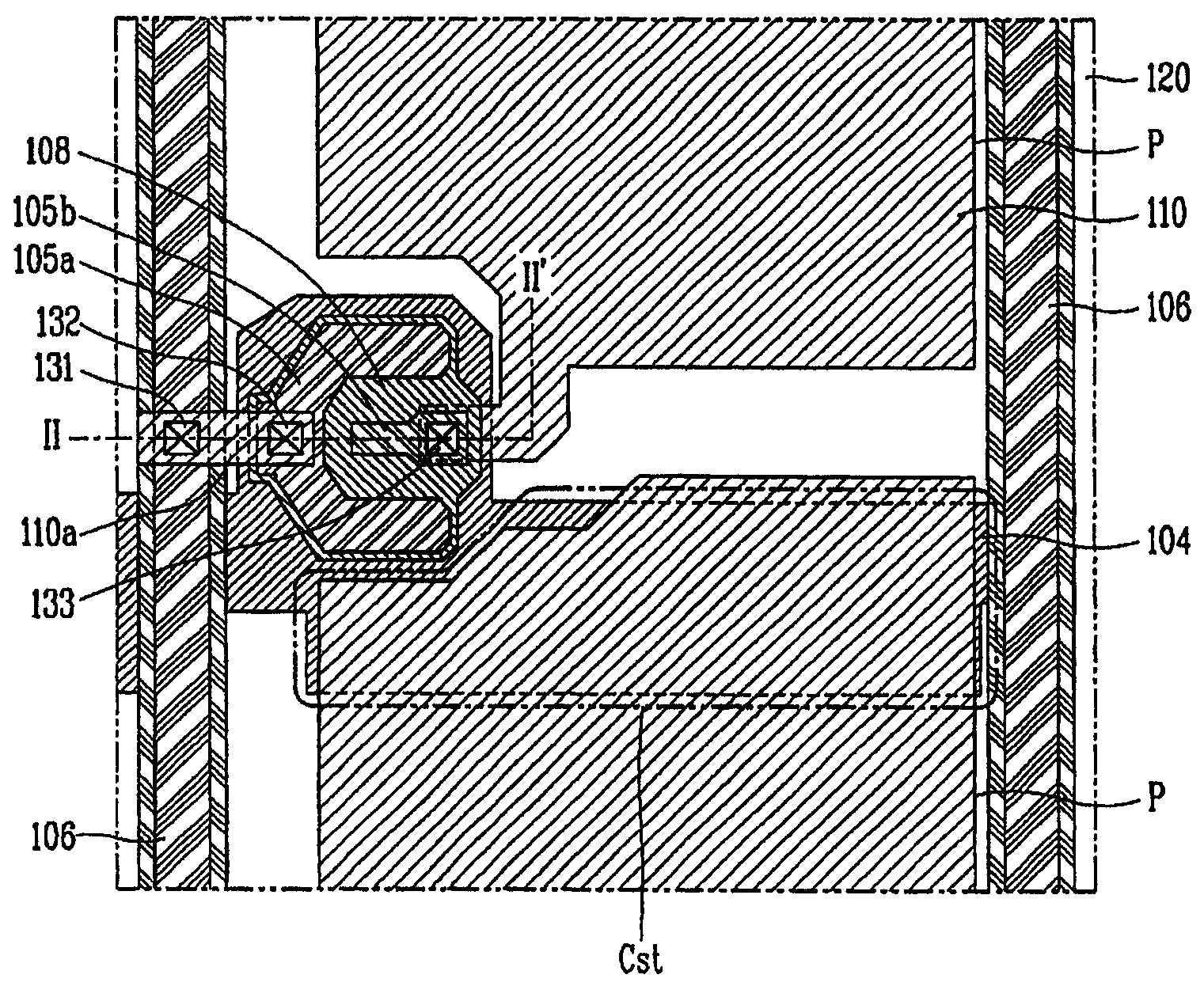
图3a是表示根据本发明第一实施例的液晶显示装置的平面图;3a is a plan view showing a liquid crystal display device according to a first embodiment of the present invention;
图3b是沿图3a的线II-II’截取的剖面图;Figure 3b is a sectional view taken along line II-II' of Figure 3a;
图4a是表示根据本发明第二实施例的液晶显示装置的平面图;4a is a plan view showing a liquid crystal display device according to a second embodiment of the present invention;
图4b是沿图4a的线III-III’截取的剖面图;Figure 4b is a sectional view taken along line III-III' of Figure 4a;
图5a至5d是表示根据本发明的液晶显示装置的制造方法的剖面图;以及5a to 5d are sectional views showing a method of manufacturing a liquid crystal display device according to the present invention; and
图6a至6c是表示根据本发明的液晶显示装置的制造方法的平面图。6a to 6c are plan views showing a method of manufacturing a liquid crystal display device according to the present invention.
具体实施方式Detailed ways
下面将详细说明本发明的优选实施例,其实例在附图中示出。Reference will now be made in detail to preferred embodiments of the invention, examples of which are illustrated in the accompanying drawings.
下面将参照附图来说明根据本发明的能够减小漏电流的液晶显示装置及其制造方法。A liquid crystal display device capable of reducing leakage current and a method of manufacturing the same according to the present invention will be described below with reference to the accompanying drawings.
图3a和3b示出了根据本发明第一实施例的液晶显示装置。图3a是表示选通线的相邻像素的一部分的平面图,图3b是言图3a的线II-II’截取的剖面图。3a and 3b show a liquid crystal display device according to a first embodiment of the present invention. FIG. 3a is a plan view showing a part of adjacent pixels of a gate line, and FIG. 3b is a cross-sectional view taken along line II-II' of FIG. 3a.
如图3a和3b所示,液晶显示装置100包括:以第一方向排列在透明基板120上的多条选通线104;以垂直于选通线104的方向排列用于限定多个像素P的多条数据线106;以及形成在选通线104和数据线106的交叉处的TFT。这里,每个TFT都包括:从选通线104引出的栅极103;半导体层108,形成在栅极103上,并与形成在数据线106的下部的半导体图案108a隔离开;以及形成在半导体层108上与栅极103相对应的源/漏极105a和105b。As shown in Figures 3a and 3b, the liquid crystal display device 100 includes: a plurality of
在栅极103与半导体层108之间布置有栅绝缘膜111。在包括数据线106和源/漏极105a和105b的基板上形成有钝化层113。A
在像素区P中形成有通过漏极接触孔113与漏极105b电连接的像素电极110。源极105b通过连接图案110a与数据线106电连接。这里,连接图案110a分别通过形成在数据线106上的第一接触孔131和形成在源极105a上的第二接触孔132与数据线106和源极105a相接触。In the pixel region P, a
像素电极110延伸至选通线104的上部,用于与选通线104形成存储电容器Cst。另外,在钝化层113上形成有像素电极110和连接图案110a。The
如上所述,在这种液晶显示装置中,形成在数据线106的下部的半导体图案108a与TFT的半导体层108彼此隔离开,用于防止背光导致的漏电流。As described above, in such a liquid crystal display device, the
通常,在由4掩模工艺制得的液晶显示装置中,在数据线的下部形成有半导体图案,TFT的源极从数据线延伸至半导体层的上部。因此,半导体图案沿源极形成并与半导体层结合。结果,半导体图案形成在数据线与半导体层之间,且暴露给背光的光,由此产生漏电流(参见图2)。Generally, in a liquid crystal display device manufactured by a 4-mask process, a semiconductor pattern is formed under a data line, and a source of a TFT extends from the data line to an upper portion of the semiconductor layer. Accordingly, a semiconductor pattern is formed along the source and combined with the semiconductor layer. As a result, a semiconductor pattern is formed between the data line and the semiconductor layer, and is exposed to light of a backlight, thereby generating leakage current (see FIG. 2 ).
相反,根据本发明,形成在数据线106与半导体层108之间的半导体图案被去除,从而防止了背光产生漏电流。数据线106和源极105a通过连接图案110a彼此电连接。特别地,半导体层108和源极105a以及漏极105b形成在栅极103的区域中,通过栅极103完全遮断了背光的光。On the contrary, according to the present invention, the semiconductor pattern formed between the
因此,由于去除了暴露给背光的光的半导体图案而不会产生漏电流。尽管与数据线相对应地形成半导体图案,但是该半导体图案与半导体层隔离开来,不会在TFT中产生漏电流。Therefore, no leakage current is generated due to the removal of the semiconductor pattern exposed to the light of the backlight. Although the semiconductor pattern is formed corresponding to the data line, the semiconductor pattern is isolated from the semiconductor layer and does not generate leakage current in the TFT.
这种液晶显示装置可通过4掩模工艺制得。即,通过第一掩模工艺形成栅极和选通线,通过第二掩模工艺形成半导体层、源极和漏极以及数据线。在第二掩模工艺中使用衍射掩模(或半调掩模)。通过第三掩模工艺形成接触孔(漏接触孔等),通过第四掩模工艺形成像素电极。Such a liquid crystal display device can be fabricated through a 4-mask process. That is, gates and gate lines are formed through a first mask process, and semiconductor layers, source and drain electrodes, and data lines are formed through a second mask process. A diffraction mask (or halftone mask) is used in the second mask process. A contact hole (drain contact hole, etc.) is formed through a third mask process, and a pixel electrode is formed through a fourth mask process.
另一方面,这种液晶显示装置还可以通过3掩模工艺制得。图4a和4b示出了通过3掩模工艺制得的液晶显示装置。图4a是平面图,而图4b是沿图4a的线III-III’截取的剖面图。On the other hand, this liquid crystal display device can also be manufactured through a 3-mask process. 4a and 4b show a liquid crystal display device fabricated by a 3-mask process. Fig. 4a is a plan view, and Fig. 4b is a sectional view taken along line III-III' of Fig. 4a.
除了像素电极的形成位置以外,图4a和4b的液晶显示装置的整体结构与图3a和3b的液晶显示装置的相同。下面将对结构差别进行说明。The overall structure of the liquid crystal display device of FIGS. 4a and 4b is the same as that of the liquid crystal display device of FIGS. 3a and 3b except for the formation position of the pixel electrode. The structural differences will be explained below.
如图4a和4b所示,源极205a和数据线206形成有预定间隔,并通过连接图案210a彼此电连接。连接图案210a的一侧与数据线206的一侧相接触,而其另一侧与源极205的一侧相接触,由此使数据线206和源极205a电连接。这里,源极205a被形成为U形以形成U形沟道,从而增大TFT的开关速度。在由选通线204和数据线206限定的像素区P中形成有与TFT的漏极205b相接触的像素电极210。像素电极210的一部分还与漏极205b的一侧相接触。As shown in FIGS. 4a and 4b, the source electrode 205a and the data line 206 are formed with a predetermined interval and are electrically connected to each other through the connection pattern 210a. One side of the connection pattern 210a is in contact with one side of the data line 206, and the other side thereof is in contact with one side of the source electrode 205, thereby electrically connecting the data line 206 and the source electrode 205a. Here, the source electrode 205a is formed in a U shape to form a U-shaped channel, thereby increasing the switching speed of the TFT. A pixel electrode 210 in contact with the drain electrode 205 b of the TFT is formed in the pixel region P defined by the gate line 204 and the data line 206 . A part of the pixel electrode 210 is also in contact with one side of the drain electrode 205b.
另一方面,栅绝缘膜211形成在栅极203上,连接图案210a和像素图案210形成在栅绝缘膜211上。由SiOx制成的钝化层213形成在暴露在源极205a与漏极205b之间的半导体层上。钝化层213可以形成在基板的包括源极205a和漏极205b的整个表面上。然而,如果将钝化层213形成在基板的整个表面上,就必须暴露出用于和驱动单元相连的焊盘单元(未示出)。因此,增大了掩模工艺数。然而,钝化层213可以仅形成在通过Q2等离子体而露出的半导体层上,而不会增加掩模工艺。On the other hand, a gate insulating film 211 is formed on the gate electrode 203 , and a connection pattern 210 a and a pixel pattern 210 are formed on the gate insulating film 211 . A passivation layer 213 made of SiOx is formed on the semiconductor layer exposed between the source electrode 205a and the drain electrode 205b. A passivation layer 213 may be formed on the entire surface of the substrate including the source electrode 205a and the drain electrode 205b. However, if the passivation layer 213 is formed on the entire surface of the substrate, a pad unit (not shown) for connection with the driving unit must be exposed. Therefore, the number of mask processes increases. However, the passivation layer 213 may be formed only on the semiconductor layer exposed by the Q2 plasma without increasing the mask process.
下面将参照附图来说明使用3掩模工艺的液晶显示装置制造方法。Hereinafter, a method of manufacturing a liquid crystal display device using a 3-mask process will be described with reference to the accompanying drawings.
图5a至5d和图6a至6c示出了根据本发明的液晶显示装置的制造方法。图5a至5d是剖面图,图6a至6c是平面图。5a to 5d and 6a to 6c illustrate a method of manufacturing a liquid crystal display device according to the present invention. 5a to 5d are sectional views, and FIGS. 6a to 6c are plan views.
如图5a和6a所示,制备透明基板,通过第一掩模工艺在该基板上形成选通线304以及从选通线304引出的TFT的栅极303。在基板的包括栅极303的整个表面上形成栅绝缘膜311。通过第二掩模工艺,分别在栅绝缘膜311上形成半导体图案308a和TFT的半导体层308。这里,形成半导体图案308a是为了对稍后形成的数据线306进行修补。半导体层308被形成为与栅极303相对应。PR图案350用作形成半导体图案308a和半导体层308所用的掩模,其并未被去除。As shown in FIGS. 5 a and 6 a , a transparent substrate is prepared, and a gate line 304 and a
如图5b所示,在基板的包括PR图案的整个表面上淀积透明导电材料,例如ITO或IZO,并去除PR图案350。因此,如图5c所示,在像素区P中形成了像素电极310,并形成了连接图案310a,以使半导体图案308a与TFT的半导体层308相连接。As shown in FIG. 5b, a transparent conductive material, such as ITO or IZO, is deposited on the entire surface of the substrate including the PR pattern, and the
参照图5d和6d,通过第三掩模工艺形成:数据线306,与选通线304垂直交叉并部分接触连接图案310a的一侧;源极305a,形成在半导体层308上,并与数据线306间隔有预定的间隔,其一侧与连接图案310a的另一侧相连,以与数据线306电连接;以及漏极305b,形成在半导体层308上,并与源极305a间隔有预定的间隔,其一侧与像素电极310的一部分相连。Referring to Figures 5d and 6d, a third mask process is used to form: a
如图5d和6c所示,在暴露在源极305a和漏极305b之间的半导体层308上通过Q2等离子体工艺形成由SiOx制成的钝化层313。半导体层308由a-Si制成。当对a-Si的表面进行Q2等离子工艺时,会在其上形成SiOx。As shown in FIGS. 5d and 6c, a
使用3掩模工艺的液晶显示装置的制造方法简化了整个工艺,并通过省略昂贵的衍射掩模而缩减的工艺成本。The manufacturing method of the liquid crystal display device using the 3-mask process simplifies the overall process and reduces the process cost by omitting the expensive diffraction mask.
如上所述,本发明提供了一种能够防止背光所产生的漏电流的液晶显示装置,以及其制造方法。即,形成在数据线下部的半导体图案和TFT的半导体层彼此隔离开,从而去除了暴露给背光的光的半导体图案。因此,TFT的源极与数据线分隔开预定间隔,并通过利用像素电极形成的连接图案与数据线电连接。As described above, the present invention provides a liquid crystal display device capable of preventing leakage current generated by a backlight, and a manufacturing method thereof. That is, the semiconductor pattern formed under the data line and the semiconductor layer of the TFT are isolated from each other, thereby removing the semiconductor pattern exposed to the light of the backlight. Accordingly, the source electrode of the TFT is separated from the data line by a predetermined interval, and is electrically connected to the data line through a connection pattern formed using the pixel electrode.
结果,暴露给背光的光的半导体层被去除,从而防止了漏电流的产生。通过防止漏电流的产生,液晶显示装置的图像质量可以得到显著提高。As a result, the semiconductor layer exposed to the light of the backlight is removed, thereby preventing the generation of leakage current. By preventing the generation of leakage current, the image quality of the liquid crystal display device can be significantly improved.
因为在不脱离本发明的精神和基本特征的情况下,可以以多种形式实施本发明,所以应该理解,上述实施例并不限于以上说明书的任意细节,除非另有指定,否则应该解释为落入所附权利要求中所限定的本发明的精神和范围内,因此,所附权利要求旨在涵盖落入其范围或者等同范围内的所有改变和修改。Because the invention can be embodied in various forms without departing from the spirit and essential characteristics of the invention, it should be understood that the above-described embodiments are not limited to any details of the above description, and unless otherwise specified, should be construed as falling into the Being within the spirit and scope of the invention as defined in the appended claims, the appended claims are therefore intended to cover all changes and modifications which come within the scope or equivalents thereof.
Claims (19)
Applications Claiming Priority (2)
| Application Number | Priority Date | Filing Date | Title |
|---|---|---|---|
| KR1020050055963A KR101152528B1 (en) | 2005-06-27 | 2005-06-27 | Liquid crystal display device capable of reducing leakage current and fabrication method thereof |
| KR1020050055963 | 2005-06-27 |
Publications (2)
| Publication Number | Publication Date |
|---|---|
| CN1892386A true CN1892386A (en) | 2007-01-10 |
| CN100454122C CN100454122C (en) | 2009-01-21 |
Family
ID=37513766
Family Applications (1)
| Application Number | Title | Priority Date | Filing Date |
|---|---|---|---|
| CNB2006100947007A Expired - Fee Related CN100454122C (en) | 2005-06-27 | 2006-06-26 | Liquid crystal display device capable of reducing leakage current and manufacturing method thereof |
Country Status (6)
| Country | Link |
|---|---|
| US (1) | US8134155B2 (en) |
| JP (1) | JP4473235B2 (en) |
| KR (1) | KR101152528B1 (en) |
| CN (1) | CN100454122C (en) |
| DE (1) | DE102006028320B4 (en) |
| TW (1) | TWI337406B (en) |
Cited By (2)
| Publication number | Priority date | Publication date | Assignee | Title |
|---|---|---|---|---|
| CN100428039C (en) * | 2005-11-23 | 2008-10-22 | 北京京东方光电科技有限公司 | A TFT LCD pixel structure |
| CN105870197A (en) * | 2016-04-21 | 2016-08-17 | 京东方科技集团股份有限公司 | Thin film transistor, fabrication method thereof, array substrate and display device |
Families Citing this family (14)
| Publication number | Priority date | Publication date | Assignee | Title |
|---|---|---|---|---|
| CN101416320B (en) * | 2006-01-31 | 2011-08-31 | 出光兴产株式会社 | TFT substrate, reflective TFT substrate, and manufacturing method thereof |
| KR101330399B1 (en) * | 2007-02-02 | 2013-11-15 | 엘지디스플레이 주식회사 | Thin film transistor device for liquid crystal display and manufacturing method thereof |
| US9176353B2 (en) | 2007-06-29 | 2015-11-03 | Semiconductor Energy Laboratory Co., Ltd. | Liquid crystal display device |
| US7738050B2 (en) * | 2007-07-06 | 2010-06-15 | Semiconductor Energy Laboratory Co., Ltd | Liquid crystal display device |
| US7897971B2 (en) * | 2007-07-26 | 2011-03-01 | Semiconductor Energy Laboratory Co., Ltd. | Display device |
| US8786793B2 (en) * | 2007-07-27 | 2014-07-22 | Semiconductor Energy Laboratory Co., Ltd. | Display device and manufacturing method thereof |
| JP2009105390A (en) * | 2007-10-05 | 2009-05-14 | Semiconductor Energy Lab Co Ltd | Semiconductor device and manufacturing method thereof |
| JP5377940B2 (en) * | 2007-12-03 | 2013-12-25 | 株式会社半導体エネルギー研究所 | Semiconductor device |
| JP5615605B2 (en) * | 2010-07-05 | 2014-10-29 | 三菱電機株式会社 | FFS mode liquid crystal device |
| JP2012053372A (en) * | 2010-09-03 | 2012-03-15 | Hitachi Displays Ltd | Liquid crystal display device |
| KR101789236B1 (en) | 2010-12-24 | 2017-10-24 | 삼성디스플레이 주식회사 | Thin film transistor and flat display device |
| CN103187423B (en) | 2013-02-04 | 2016-03-23 | 合肥京东方光电科技有限公司 | A kind of oxide film transistor array substrate and preparation method thereof, display floater |
| CN203983289U (en) * | 2014-06-17 | 2014-12-03 | 京东方科技集团股份有限公司 | Thin-film transistor, array base palte and display unit |
| CN104752345B (en) * | 2015-04-27 | 2018-01-30 | 深圳市华星光电技术有限公司 | Thin-film transistor array base-plate and preparation method thereof |
Family Cites Families (9)
| Publication number | Priority date | Publication date | Assignee | Title |
|---|---|---|---|---|
| JP3002099B2 (en) | 1994-10-13 | 2000-01-24 | 株式会社フロンテック | Thin film transistor and liquid crystal display device using the same |
| JP3716580B2 (en) * | 1997-02-27 | 2005-11-16 | セイコーエプソン株式会社 | Liquid crystal device and manufacturing method thereof, and projection display device |
| JPH1140814A (en) | 1997-07-18 | 1999-02-12 | Furontetsuku:Kk | Thin film transistor substrate, liquid crystal display device, and method of manufacturing thin film transistor substrate |
| JP4100655B2 (en) * | 1999-12-21 | 2008-06-11 | エルジー.フィリップス エルシーデー カンパニー,リミテッド | Thin film transistor manufacturing method |
| JP4211250B2 (en) | 2000-10-12 | 2009-01-21 | セイコーエプソン株式会社 | Transistor and display device including the same |
| KR100743101B1 (en) * | 2001-05-07 | 2007-07-27 | 엘지.필립스 엘시디 주식회사 | Liquid crystal display device and manufacturing method thereof and pixel repair method using same |
| JP4604440B2 (en) * | 2002-02-22 | 2011-01-05 | 日本電気株式会社 | Channel etch type thin film transistor |
| JP4551049B2 (en) | 2002-03-19 | 2010-09-22 | 三菱電機株式会社 | Display device |
| JP2004342923A (en) * | 2003-05-16 | 2004-12-02 | Seiko Epson Corp | Liquid crystal device, active matrix substrate, display device, and electronic device |
-
2005
- 2005-06-27 KR KR1020050055963A patent/KR101152528B1/en not_active Expired - Fee Related
-
2006
- 2006-06-20 DE DE102006028320.1A patent/DE102006028320B4/en not_active Expired - Fee Related
- 2006-06-26 CN CNB2006100947007A patent/CN100454122C/en not_active Expired - Fee Related
- 2006-06-26 US US11/474,356 patent/US8134155B2/en not_active Expired - Fee Related
- 2006-06-27 JP JP2006176660A patent/JP4473235B2/en not_active Expired - Fee Related
- 2006-06-27 TW TW095123466A patent/TWI337406B/en not_active IP Right Cessation
Cited By (2)
| Publication number | Priority date | Publication date | Assignee | Title |
|---|---|---|---|---|
| CN100428039C (en) * | 2005-11-23 | 2008-10-22 | 北京京东方光电科技有限公司 | A TFT LCD pixel structure |
| CN105870197A (en) * | 2016-04-21 | 2016-08-17 | 京东方科技集团股份有限公司 | Thin film transistor, fabrication method thereof, array substrate and display device |
Also Published As
| Publication number | Publication date |
|---|---|
| KR20070000546A (en) | 2007-01-03 |
| DE102006028320B4 (en) | 2014-05-22 |
| JP4473235B2 (en) | 2010-06-02 |
| JP2007011351A (en) | 2007-01-18 |
| US8134155B2 (en) | 2012-03-13 |
| US20060289867A1 (en) | 2006-12-28 |
| DE102006028320A1 (en) | 2006-12-28 |
| KR101152528B1 (en) | 2012-06-01 |
| TWI337406B (en) | 2011-02-11 |
| TW200709426A (en) | 2007-03-01 |
| CN100454122C (en) | 2009-01-21 |
Similar Documents
| Publication | Publication Date | Title |
|---|---|---|
| CN1324387C (en) | Array baseboard of LCD and its producing method | |
| CN100335957C (en) | In-plane switching mode liquid crystal display device and method for fabricating the same | |
| CN1222048C (en) | Transistor and display comprising it | |
| CN100335958C (en) | IPS type LCD and method for fabricating the same | |
| CN1716067A (en) | Liquid crystal display device and manufacturing method thereof | |
| CN1892386A (en) | Liquid crystal display device capable of reducing leakage current, and fabrication method thereof | |
| CN1773356A (en) | Liquid crystal display device and manufacturing method thereof | |
| CN1495477A (en) | Display substrate, liquid crystal display and method of manufacturing the liquid crystal display | |
| CN102566168A (en) | Array substrate, manufacturing method thereof and liquid crystal display device | |
| CN101064322A (en) | Electro-optical device and electronic apparatus | |
| CN1280308A (en) | Film transistor array and its producing method | |
| CN1503042A (en) | TFT array circuit board and its manufacturing method | |
| CN1862349A (en) | Liquid crystal display and manufacturing method therefor | |
| CN1255701C (en) | Active matrix crystal display devices and manufacturing methods thereof | |
| CN1834758A (en) | In-plane switching mode liquid crystal display device and fabrication method thereof | |
| CN1637546A (en) | Array substrate for a transflective liquid crystal display device and fabricating method thereof | |
| CN1628264A (en) | Thin film transistor array panel for a liquid crystal display | |
| CN1991544A (en) | Liquid crystal display device and method of manufacturing the same | |
| CN1797162A (en) | Liquid crystal display device and fabricating method thereof | |
| CN1584712A (en) | Liquid crystal display panel with narrow frame design and manufacturing method thereof | |
| CN1637539A (en) | Liquid crystal display device and method for fabricating the same | |
| CN1342965A (en) | Display panel and display equipment | |
| CN1641450A (en) | Liquid crystal display and manufacturing method thereof, transistor array substrate and manufacturing method thereof | |
| CN1256618C (en) | Liquid crystal display and manufacturing method thereof | |
| CN1716632A (en) | Double gate thin film transistor, pixel structure and manufacturing method thereof |
Legal Events
| Date | Code | Title | Description |
|---|---|---|---|
| C06 | Publication | ||
| PB01 | Publication | ||
| C10 | Entry into substantive examination | ||
| SE01 | Entry into force of request for substantive examination | ||
| C14 | Grant of patent or utility model | ||
| GR01 | Patent grant | ||
| CF01 | Termination of patent right due to non-payment of annual fee | ||
| CF01 | Termination of patent right due to non-payment of annual fee |
Granted publication date: 20090121 Termination date: 20200626 |