CN1866557A - Light-emitting device, method for making the same, and nitride semiconductor substrate - Google Patents
Light-emitting device, method for making the same, and nitride semiconductor substrate Download PDFInfo
- Publication number
- CN1866557A CN1866557A CNA2006100092371A CN200610009237A CN1866557A CN 1866557 A CN1866557 A CN 1866557A CN A2006100092371 A CNA2006100092371 A CN A2006100092371A CN 200610009237 A CN200610009237 A CN 200610009237A CN 1866557 A CN1866557 A CN 1866557A
- Authority
- CN
- China
- Prior art keywords
- light
- layer
- semiconductor substrate
- type
- emitting device
- Prior art date
- Legal status (The legal status is an assumption and is not a legal conclusion. Google has not performed a legal analysis and makes no representation as to the accuracy of the status listed.)
- Pending
Links
Images


Classifications
-
- H—ELECTRICITY
- H10—SEMICONDUCTOR DEVICES; ELECTRIC SOLID-STATE DEVICES NOT OTHERWISE PROVIDED FOR
- H10H—INORGANIC LIGHT-EMITTING SEMICONDUCTOR DEVICES HAVING POTENTIAL BARRIERS
- H10H20/00—Individual inorganic light-emitting semiconductor devices having potential barriers, e.g. light-emitting diodes [LED]
- H10H20/80—Constructional details
- H10H20/81—Bodies
- H10H20/819—Bodies characterised by their shape, e.g. curved or truncated substrates
-
- H—ELECTRICITY
- H10—SEMICONDUCTOR DEVICES; ELECTRIC SOLID-STATE DEVICES NOT OTHERWISE PROVIDED FOR
- H10H—INORGANIC LIGHT-EMITTING SEMICONDUCTOR DEVICES HAVING POTENTIAL BARRIERS
- H10H20/00—Individual inorganic light-emitting semiconductor devices having potential barriers, e.g. light-emitting diodes [LED]
- H10H20/80—Constructional details
- H10H20/81—Bodies
- H10H20/822—Materials of the light-emitting regions
- H10H20/824—Materials of the light-emitting regions comprising only Group III-V materials, e.g. GaP
- H10H20/825—Materials of the light-emitting regions comprising only Group III-V materials, e.g. GaP containing nitrogen, e.g. GaN
-
- H10W72/884—
Landscapes
- Led Devices (AREA)
- Drying Of Semiconductors (AREA)
- Led Device Packages (AREA)
Abstract
根据本发明的发光器件,包括:GaN衬底(1);GaN衬底(1)的第一主表面侧上的n型AlxGa1-xN层(3);与n型AlxGa1-xN层(3)相比更远离GaN衬底(1)设置的p型AlxGa1-xN层(5);以及位于n型AlxGa1-xN层(3)和p型AlxGa1-xN层(5)之间的多量子阱(MQW)(4)。在该发光器件中,p型AlxGa1-xN层(5)侧被向下安装,以及光从第二主表面(1a)发射,其中第二主表面是与第一主表面相对的GaN衬底(1)的主表面。在GaN衬底(1)的第二主表面(1a)上形成半球形凸部(82)。
A light-emitting device according to the present invention, comprising: a GaN substrate (1); an n-type AlxGa1 -xN layer (3) on the first main surface side of the GaN substrate (1); and an n-type AlxGa The p-type Al x Ga 1-x N layer (5) arranged farther away from the GaN substrate (1) than the 1-x N layer (3); and the n-type Al x Ga 1-x N layer (3) and Multiple quantum wells (MQW) (4) between p-type AlxGa1 -xN layers (5). In the light emitting device, the p-type AlxGa1 -xN layer (5) side is mounted downward, and light is emitted from the second main surface (1a), which is opposite to the first main surface The main surface of the GaN substrate (1). A hemispherical protrusion (82) is formed on the second main surface (1a) of the GaN substrate (1).
Description
技术领域technical field
本发明涉及一种发光器件及其制造方法,以及一种氮化物半导体衬底。更具体地说,本发明涉及由氮化物半导体形成的发光器件及其制造方法,以及氮化物半导体衬底。在本发明中,“发光器件”可以指基本上由氮化物半导体衬底和其上层叠的半导体层形成的半导体元件,或可以单独地指半导体芯片,或可以单独地指密封在树脂中的、具有安装在安装部件中的半导体芯片的器件。而且,也可以同时以两种含义使用该术语。此外,半导体芯片也可以被单独地称为“芯片”。此外,在芯片中,衬底和其上形成的外延层可以简单地称为“衬底”。The invention relates to a light-emitting device, a manufacturing method thereof, and a nitride semiconductor substrate. More specifically, the present invention relates to a light emitting device formed of a nitride semiconductor, a method of manufacturing the same, and a nitride semiconductor substrate. In the present invention, a "light emitting device" may refer to a semiconductor element formed substantially from a nitride semiconductor substrate and a semiconductor layer laminated thereon, or may refer to a semiconductor chip alone, or may refer to a semiconductor chip sealed in a resin alone, A device having a semiconductor chip mounted in a mounting part. Moreover, the term can also be used in both senses at the same time. In addition, a semiconductor chip may also be referred to as a "chip" individually. Also, in a chip, a substrate and an epitaxial layer formed thereon may simply be referred to as a "substrate".
背景技术Background technique
目前,白色发光二极管(LED)通常用于照明和紧凑的电子设备,如便携式信息终端。但是,它们将来可以用于大空间中或大面积上的照明的可能性是存在的。为了使LED用于大空间和大面积的照明成为可能,必须增加LED的光输出。Currently, white light-emitting diodes (LEDs) are commonly used for lighting and compact electronic devices such as portable information terminals. However, the possibility exists that they may be used for lighting in large spaces or over large areas in the future. In order to make it possible for LEDs to be used for lighting large spaces and large areas, it is necessary to increase the light output of LEDs.
用于增加LED的光输出的一种方法是将LED内产生的光有效地输出到外面,即,增加光提取效率。用于增加光提取效率的常规技术的例子包括:发光器件具有由蓝宝石等形成的衬底,其中使用喷砂(blasting)处理在与形成氮化物半导体层的表面相对的后表面上形成具有凸凹形状的光反射表面(例如,参见日本特开专利公开号2004-56088);一种发光器件,其中在由蓝宝石等形成的衬底的上述后表面上采用沟槽形成和研磨相结合形成能够作为透镜的弯曲形状;以及在蓝宝石衬底上层叠的氮化镓(GaN)器件,在GaN层上形成电极和通过刻蚀n-GaN层表面来在n-GaN表面上形成具有0.5-1微米直径的半球形凸部(例如,非专利文献:D.W.Kim和其它三人的″Highly efficientvertical laser-liftoff GaN-based light-emitting diodes formed byoptimization of the cathode structure″,Applied Physics Letters 86,052108(2005))。One method for increasing the light output of an LED is to efficiently output light generated within the LED to the outside, ie, to increase light extraction efficiency. Examples of conventional techniques for increasing light extraction efficiency include: a light-emitting device having a substrate formed of sapphire or the like, in which a surface having a convex-concave shape is formed on the rear surface opposite to the surface on which the nitride semiconductor layer is formed using a blasting process. (for example, see Japanese Laid-Open Patent Publication No. 2004-56088); a light-emitting device in which a combination of groove formation and grinding is used to form a lens capable of serving as a lens on the above-mentioned rear surface of a substrate formed of sapphire or the like curved shape; and gallium nitride (GaN) devices stacked on a sapphire substrate, forming electrodes on the GaN layer and forming a 0.5-1 micron diameter electrode on the n-GaN surface by etching the surface of the n-GaN layer Hemispherical convex portion (for example, non-patent literature: "Highly efficient vertical laser-liftoff GaN-based light-emitting diodes formed by optimization of the cathode structure" by D.W. Kim and others, Applied Physics Letters 86, 052108 (2005)).
在日本特开专利公开号2004-56088中公开的发光器件中,执行喷砂处理,以形成凸凹形状,但是当使用该方法时精确地控制凹/凸形的形状是困难的。此外,在日本特开专利公开号2004-56088中,还给出使用划片机和激光处理作为用于形成反射表面的方法的例子,但是利用这些方法形成诸如半球形表面的形状是困难的。In the light emitting device disclosed in Japanese Laid-Open Patent Publication No. 2004-56088, sandblasting is performed to form a concave-convex shape, but it is difficult to precisely control the concave/convex shape when this method is used. Furthermore, in Japanese Laid-Open Patent Publication No. 2004-56088, examples are also given of using a dicing machine and laser processing as methods for forming a reflective surface, but it is difficult to form a shape such as a hemispherical surface with these methods.
此外,在日本专利号3362836的说明书中,通过使用划片机或激光形成沟槽,然后进行研磨,来形成弯曲的表面形状,但是由于该方法结合划片机步骤和研磨步骤,与简单地使用划片机相比,增加了制作步骤的数目。结果,增加了发光器件的制作成本。Furthermore, in the specification of Japanese Patent No. 3362836, a curved surface shape is formed by forming grooves using a dicing machine or a laser followed by grinding, but since this method combines a dicing machine step and a grinding step, it is different from simply using Compared with the dicing machine, the number of production steps is increased. As a result, the manufacturing cost of the light emitting device increases.
在上述非专利文献中,通过刻蚀蓝宝石衬底上层叠的GaN层(n-GaN层)的表面来形成半球形凸部,以致形成的凸部的直径受层叠的GaN层的厚度限制。更具体地说,为了形成有较大直径的凸部,GaN层必须层叠足够的厚度,但是用于较厚的GaN层的层叠步骤需要更多时间,导致发光器件的制作成本增加。In the above non-patent literature, hemispherical protrusions are formed by etching the surface of a GaN layer (n-GaN layer) stacked on a sapphire substrate so that the diameter of the formed protrusion is limited by the thickness of the stacked GaN layer. More specifically, in order to form protrusions with larger diameters, GaN layers must be stacked to a sufficient thickness, but the stacking step for thicker GaN layers requires more time, resulting in increased manufacturing costs of light emitting devices.
本发明的目的是克服这些问题和提供一种发光器件、用于制造该发光器件的方法以及可以用于制造该发光器件的氮化物半导体衬底,其中可以提高光提取效率而不增加制作成本。An object of the present invention is to overcome these problems and provide a light emitting device, a method for manufacturing the light emitting device, and a nitride semiconductor substrate usable for manufacturing the light emitting device, in which light extraction efficiency can be improved without increasing manufacturing cost.
发明内容Contents of the invention
根据本发明的发光器件是包括以下结构的发光器件:氮化物半导体衬底;在氮化物半导体衬底的第一主表面侧上布置的n型氮化物半导体层;与该n型氮化物半导体层相比,更远离氮化物半导体衬底设置的p型氮化物半导体衬底;以及位于n型氮化物半导体层和p型氮化物半导体层之间的发光层。在该发光器件中,p型氮化物半导体层侧被向下安装,以及光从氮化物半导体衬底的第二主表面发射,该第二主表面是与第一主表面相对的主表面。在氮化物半导体衬底的第二主表面上形成半球形凸部。A light-emitting device according to the present invention is a light-emitting device comprising the following structure: a nitride semiconductor substrate; an n-type nitride semiconductor layer arranged on the first main surface side of the nitride semiconductor substrate; and the n-type nitride semiconductor layer In contrast, a p-type nitride semiconductor substrate disposed farther from the nitride semiconductor substrate; and a light emitting layer positioned between the n-type nitride semiconductor layer and the p-type nitride semiconductor layer. In this light emitting device, the p-type nitride semiconductor layer side is mounted downward, and light is emitted from the second main surface of the nitride semiconductor substrate, which is the main surface opposite to the first main surface. A hemispherical convex portion is formed on the second main surface of the nitride semiconductor substrate.
在该结构中,在作为氮化物半导体衬底的发光表面的第二主表面1a上形成半球形凸部,从而这些凸部起透镜的作用以允许垂直于第二主表面的光的有效提取。结果,当仅仅使用KOH溶液等对第二主表面进行非镜面化抛光,或通过切割等在第二主表面上形成沟槽时,与没有形成凸部时相比较,可以增加发光器件中的光使用效率。In this structure, hemispherical convex portions are formed on the second
用于制造根据本发明的具有氮化物半导体衬底的发光器件的方法包括:用于制备氮化物半导体衬底的步骤;以及用于形成半球形凸部的步骤。在用于形成半球形凸部的步骤中,通过在氮化物半导体衬底的第二主表面上执行反应离子刻蚀而除去部分第二主表面,来形成半球形凸部,该第二主表面与形成发光层的第一主表面相对。A method for manufacturing a light emitting device having a nitride semiconductor substrate according to the present invention includes: a step for preparing a nitride semiconductor substrate; and a step for forming a hemispherical protrusion. In the step for forming the hemispherical protrusion, the hemispherical protrusion is formed by performing reactive ion etching on the second main surface of the nitride semiconductor substrate to remove part of the second main surface. It is opposite to the first main surface where the light emitting layer is formed.
结果,凸部可以使用反应离子刻蚀来形成,而不需要切割或研磨等。与执行切割等相比,这可以简化发光器件的制作步骤,因此允许以低成本制造本发明的发光器件。As a result, the convex portion can be formed using reactive ion etching without cutting or grinding or the like. This can simplify the manufacturing steps of the light emitting device compared to performing dicing or the like, thus allowing the light emitting device of the present invention to be manufactured at low cost.
在本发明的氮化物半导体衬底中,在一个主表面上形成半球形凸部。当使用该氮化物半导体衬底来制造发光器件时,使用形成凸部的表面作为发光器件的光提取表面,与使用没有凸部的衬底相比,这可以制造具有高的光提取效率的发光器件。In the nitride semiconductor substrate of the present invention, hemispherical protrusions are formed on one main surface. When this nitride semiconductor substrate is used to manufacture a light-emitting device, the surface on which the protrusions are formed is used as the light-extracting surface of the light-emitting device, which can produce light-emitting devices with high light-extraction efficiency compared to using a substrate without protrusions. device.
氮化物半导体“衬底”指具有足够的厚度以允许被单独运载且不同于“膜”和“层”的板状物体,“膜”和“层”在运载过程中不独立地保持它们自己的形状。Nitride semiconductor "substrate" refers to a plate-shaped object having a thickness sufficient to allow it to be carried alone and is different from "film" and "layer" which do not independently maintain their own during carrying shape.
利用本发明,在氮化物半导体衬底的第二主表面上形成半球形凸部,以便在使用该氮化物半导体衬底的发光器件中,可以提高光提取效率。With the present invention, hemispherical protrusions are formed on the second main surface of a nitride semiconductor substrate, so that light extraction efficiency can be improved in a light emitting device using the nitride semiconductor substrate.
附图说明Description of drawings
图1是示出了用作根据本发明的发光器件的LED的第一实施例的图。FIG. 1 is a diagram showing a first embodiment of an LED used as a light emitting device according to the present invention.
图2是示出了包含图1中的LED的发光层的层状结构的图。FIG. 2 is a diagram showing a layered structure including a light emitting layer of the LED in FIG. 1 .
图3是示出了用于制造图1和图2所示的LED中使用的芯片的方法的流程图。FIG. 3 is a flowchart illustrating a method for manufacturing a chip used in the LED shown in FIGS. 1 and 2 .
图4是示出了由晶片获得具有图2所示结构的芯片时,晶片的状态的图。FIG. 4 is a diagram showing the state of the wafer when a chip having the structure shown in FIG. 2 is obtained from the wafer.
图5是示出了图4所示的电极的布置的图。FIG. 5 is a diagram showing the arrangement of electrodes shown in FIG. 4 .
图6是示出了根据图1至图5所示的本发明LED的第一实施例的选择性例子的图。Fig. 6 is a diagram showing an alternative example of the first embodiment of the LED according to the present invention shown in Figs. 1 to 5 .
图7是示出了图6的LED的平面图。FIG. 7 is a plan view illustrating the LED of FIG. 6 .
图8是示出了由晶片获得具有图6和7所示的LED中使用的层状结构的芯片时,晶片的状态的图。FIG. 8 is a diagram showing the state of the wafer when a chip having the layered structure used in the LED shown in FIGS. 6 and 7 is obtained from the wafer.
图9是示出了根据本发明的GaN衬底的第二实施例的简化图,该GaN衬底包括将形成本发明的发光器件中使用的芯片的多个区域。Fig. 9 is a simplified diagram showing a second embodiment of a GaN substrate according to the present invention, the GaN substrate including a plurality of regions that will form a chip used in a light emitting device of the present invention.
图10是图9所示的区域X的简化细节平面图。FIG. 10 is a simplified detailed plan view of area X shown in FIG. 9 .
图11是沿图10中的XI-XI线段的简化剖面图。Fig. 11 is a simplified sectional view along line XI-XI in Fig. 10 .
图12示出了LED的第二比较样品的简化图。Figure 12 shows a simplified diagram of a second comparative sample of LEDs.
图13是示出了由半球形凸部高度和光输出之间的关系的模拟所确定的结果的曲线。FIG. 13 is a graph showing the results determined from the simulation of the relationship between the height of the hemispherical convex portion and the light output.
图14是示出了氧浓度对GaN衬底的比电阻的影响的图。FIG. 14 is a graph showing the effect of oxygen concentration on the specific resistance of a GaN substrate.
图15是示出了当GaN衬底的厚度是400微米时,氧浓度对具有450nm波长的光的透射率的影响的图。FIG. 15 is a graph showing the influence of oxygen concentration on the transmittance of light having a wavelength of 450 nm when the thickness of the GaN substrate is 400 micrometers.
图16是示出了对于根据图1所示的本发明的LED,当由具有不同厚度和氧浓度的GaN衬底制造灯时,灯的光输出和电流通过其均匀地流动的平面尺寸的测量结果的图。16 is a measurement showing the light output of the lamp and the plane size through which current flows uniformly when the lamp is fabricated from GaN substrates having different thicknesses and oxygen concentrations for the LED according to the present invention shown in FIG. 1 A graph of the results.
具体实施方式Detailed ways
接下来,将使用这些图描述本发明的实施例和例子。在下面的图中,相似或相关的元件被指定相同的数字,并且它们的描述将不被重复。Next, embodiments and examples of the present invention will be described using these drawings. In the following figures, similar or related elements are assigned the same numerals, and their descriptions will not be repeated.
(第一实施例)(first embodiment)
图1示出了用作根据本发明的发光器件的LED的第一实施例。图2示出了包含图1中的LED的发光层的层状结构。下面将参考图1和2描述根据本发明的LED的第一实施例。Fig. 1 shows a first embodiment of an LED used as a light emitting device according to the present invention. FIG. 2 shows a layered structure comprising a light-emitting layer of the LED in FIG. 1 . A first embodiment of an LED according to the invention will be described below with reference to FIGS. 1 and 2 .
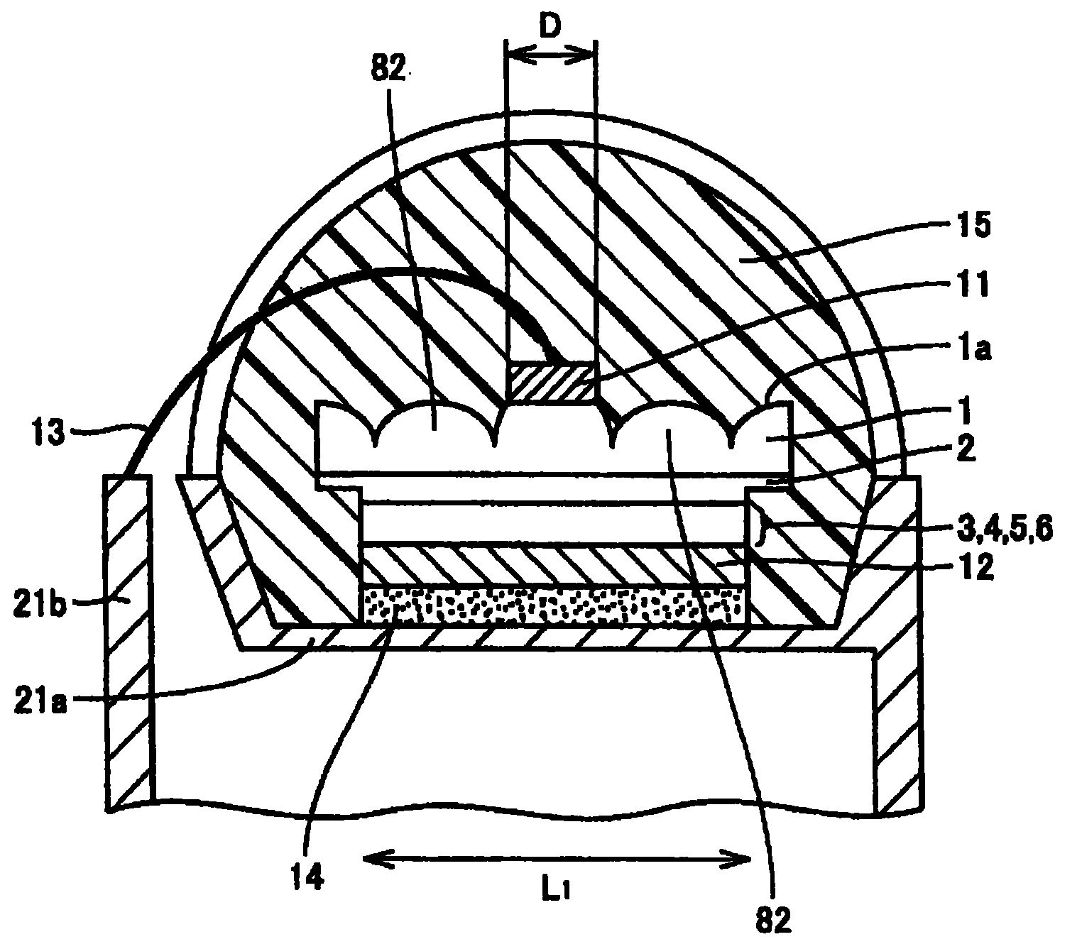
如图1所示,在GaN衬底1的第一主表面侧形成p电极12和包含之后将详细描述的发光层等的层状结构。在该实施例中,使用导电粘结剂14将p电极12向下安装在引线框座21a上。As shown in FIG. 1 , a p-
GaN衬底1的第二主表面1a是从发光层发射光的表面,以及在该表面上布置n电极11。在第二主表面1a上使用反应离子刻蚀(RIE)形成多个半球形凸部82。n电极11被大致布置在第二主表面1a的中心,以便它不覆盖整个第二主表面。n电极11可以被布置为以便它覆盖凸部82中的一个凸部的顶点。此外,n电极11可以被布置为它完全地覆盖凸部82中的一个凸部,或它可以被布置为覆盖多个凸部82。但是,存在不被n电极11覆盖的高比例是重要的。如果开口比率高,那么就减少了由于n电极11阻挡的光,并增加了发射到外部的光的发射效率。Second
n电极11通过导线13电连接到引线21b。导线13和上述层状结构用作为密封部件的环氧基树脂15密封。在上述结构中,图2示出了从GaN衬底1至p电极12的层状结构的细节。在图2中,图1中的层状结构被垂直地反转。The n-
如图2所示,在GaN衬底1上形成n型GaN外延层2,以及其上形成n型AlxGa1-xN层3。在该结构上形成由AlxGa1-xN层和AlxInyGa1-x-yN层形成的多量子阱(MQW)4。p型AlxGa1-xN层5被布置为在它和n型AlxGa1-xN层3之间插入多量子阱4。此外,在p型AlxGa1-xN层5上布置p型GaN层6。在上述结构中,在多量子阱4处发射光。此外,如图1所示,p电极12形成在p型GaN层6上并向下安装,以便它覆盖p型GaN层6的整个上表面。As shown in FIG. 2, an n-type
接下来,将参考图3至图5,简要地描述用于制造图1和图2所示的LED的方法。图3是示出了用于制造图1和图2所示的LED中使用的芯片的方法的流程图。图4示出了由晶片获得具有图2所示结构的芯片时晶片的状态。图5是示出了图4所示的电极布置的图。Next, a method for manufacturing the LED shown in FIGS. 1 and 2 will be briefly described with reference to FIGS. 3 to 5 . FIG. 3 is a flowchart illustrating a method for manufacturing a chip used in the LED shown in FIGS. 1 and 2 . FIG. 4 shows the state of the wafer when a chip having the structure shown in FIG. 2 is obtained from the wafer. FIG. 5 is a diagram showing the arrangement of electrodes shown in FIG. 4 .
首先,执行图3所示的衬底制备步骤(S10)。更具体地说,首先制备GaN衬底。然后,在GaN衬底的第一主表面上使用薄膜形成方法如MOCVD(金属有机物化学气相淀积),以形成下列层状结构:(Si掺杂的n型GaN层/作为限制层的Si掺杂的n型Al0.2Ga0.8N层/由GaN层和In0.15Ga0.85N层构成的多个双层结构形成的MQW(多量子阱)/作为限制层的Mg掺杂的p型Al0.2Ga0.8N层/Mg掺杂的p型GaN层)。接下来,该晶片可以被活化,以降低Mg掺杂的p型层的电阻。使用光刻和RIE(反应离子刻蚀)从Mg掺杂的p型层侧至Si掺杂的n型层利用Cl基气体刻蚀该晶片。由该刻蚀形成元件隔离沟槽25,如图4所示,并且元件被分离。First, the substrate preparation step (S10) shown in FIG. 3 is performed. More specifically, a GaN substrate is prepared first. Then, a film forming method such as MOCVD (Metal Organic Chemical Vapor Deposition) is used on the first main surface of the GaN substrate to form the following layered structure: (Si-doped n-type GaN layer/Si-doped Doped n-type Al 0.2 Ga 0.8 N layer/MQW (Multiple Quantum Well) formed by multiple double-layer structures composed of GaN layer and In 0.15 Ga 0.85 N layer/Mg-doped p-type Al 0.2 Ga as confinement layer 0.8 N layer/Mg-doped p-type GaN layer). Next, the wafer can be activated to reduce the resistance of the Mg-doped p-type layer. The wafer was etched with Cl-based gas from the Mg-doped p-type layer side to the Si-doped n-type layer using photolithography and RIE (Reactive Ion Etching). An
接下来,在作为GaN衬底的第二主表面(主表面)的后N表面上执行光刻、气相淀积和剥离,从而以预定间距(距离L2)在芯片的中心形成n电极11,当从上面观看时,n电极11具有正方形形状(参见图4和图5)。n电极11可以形成为从与GaN衬底接触的底层开始由(Ti层/Al层/Ti层/Au层)形成的层状结构。然后为了使n电极11和GaN衬底的后表面之间的接触电阻是预定值,在氮气(N2)气氛中加热GaN衬底。Next, photolithography, vapor deposition, and lift-off are performed on the rear N surface which is the second main surface (main surface) of the GaN substrate, thereby forming
接下来,形成与p型GaN层接触并具有预定厚度的导体层,以形成p电极。例如,可以通过形成具有预定厚度的Ni层来形成该导体层,以便它与GaN层接触,以及在其整个表面上形成具有预定厚度的Au层(参见图4和图5)。在此情况下,为了使p电极和p型GaN层之间的接触电阻是预定值,可以在惰性气体气氛中加热GaN衬底。Next, a conductor layer is formed in contact with the p-type GaN layer and has a predetermined thickness to form a p-electrode. For example, the conductor layer can be formed by forming a Ni layer with a predetermined thickness so that it is in contact with the GaN layer, and an Au layer with a predetermined thickness on the entire surface thereof (see FIGS. 4 and 5 ). In this case, in order to make the contact resistance between the p-electrode and the p-type GaN layer a predetermined value, the GaN substrate may be heated in an inert gas atmosphere.
接下来,执行使用图3所示的RIE(S20)来形成半球形凸部的步骤。更具体地说,在GaN衬底的后表面(N表面)上执行RIE,以形成半球形凸部82。用于RIE的反应气体可以是氯气(Cl气体)等。由于形成n电极11的N表面的区域的外周边部分被该RIE操作部分地除去,因此在n电极11的下面形成具有平坦顶表面的凸部。n电极11被布置在凸部的顶表面上。此外,RIE操作在除形成n电极11的区域以外的N表面的区域中形成半球形凸部82。凸部82的宽度W(参见图4)大约为凸部82的高度的两倍。凸部82的高度至少是0.2微米且不超过100微米。此外,可以在形成上述n电极11的步骤之前执行RIE半球形凸部步骤(S20)。Next, a step of forming a hemispherical convex portion using RIE ( S20 ) shown in FIG. 3 is performed. More specifically, RIE is performed on the rear surface (N surface) of the GaN substrate to form hemispherical
然后,如图4和图5所示,执行划片,以便芯片边界50作为侧表面出现并且所得的芯片形成发光器件。参考图1,芯片被安装,以便芯片的p型GaN层侧与引线框的安装部件21a接触,得到发光器件。被涂敷到安装部件的导电粘结剂14固定发光器件和安装部件并提供连续性。然后,在通过引线结合连接n电极和引线框的引线部件之后,环氧基树脂15将该结构密封在树脂中,从而由发光器件形成灯。此外,为了增加发光器件的散热,可以执行安装,以便发光器件的p型GaN层的整个表面与安装部件接触。此外,导电粘结剂14可以使用具有良好导热性的Ag基材料,以及引线框可以使用具有良好导热性的CuW基材料。Then, as shown in FIGS. 4 and 5 , dicing is performed so that the
图6示出了根据图1至图5所示的本发明实施例的LED的第一实施例的选择性例子。图7是示出了从上面观看时图6的LED形状的图。下面将参考图6和图7描述根据本发明的LED的第一实施例的选择性例子。Fig. 6 shows an alternative example of a first embodiment of an LED according to the embodiment of the invention shown in Figs. 1 to 5 . Fig. 7 is a diagram showing the shape of the LED of Fig. 6 when viewed from above. An optional example of the first embodiment of the LED according to the present invention will be described below with reference to FIGS. 6 and 7 .
图6和图7所示的LED具有与图1和图2所示的LED基本上相同的结构,除了n电极11被布置在GaN衬底的四个拐角附近之外。此外,在图6和图7所示的LED中,围绕安装的半导体芯片布置反光杯37。The LED shown in FIGS. 6 and 7 has substantially the same structure as the LED shown in FIGS. 1 and 2 except that n-
用于制造图6和图7所示的LED的方法基本上与用于制造图1和图2所示的LED的方法相同。图8示出了获得具有用于图6和7所示的LED的层状结构的芯片时晶片的状态。在此情况下,由于每个芯片具有较大数目的n电极11,每个n电极11的面积优选小于图1和图2所示的LED的n电极11的面积。The method for manufacturing the LED shown in FIGS. 6 and 7 is basically the same as the method for manufacturing the LED shown in FIGS. 1 and 2 . FIG. 8 shows the state of the wafer when a chip having a layered structure for the LED shown in FIGS. 6 and 7 is obtained. In this case, since each chip has a larger number of n-
(第二实施例)(second embodiment)
在上述第一实施例中,通过划片GaN衬底1获得的芯片被安装在引线框中,以形成发光器件。但是,代替将GaN衬底1分为芯片以形成发光器件,可以存在通过对如下衬底进行加工来更容易地进行处理的情况,其中在所述衬底上,执行了RIE半球形凸部形成步骤(S20)以在GaN衬底1上形成半球形凸部82。图9是示出了根据本发明的GaN衬底的第二实施例的简化图,该GaN衬底包括将形成发光器件的芯片的多个区域。图10是图9所示的区域X的简化细节图。图11是沿图10中的XI-XI线段的简化剖面图。如图9至图11所示,在第二主表面1a上形成多个半球形凸部82,第二主表面1a是GaN衬底1的主表面中的一个。通过在它们被分开之前以在GaN衬底1上形成多个芯片的方式处理它们更容易进行多个芯片的处理。In the first embodiment described above, chips obtained by dicing the
[第一例子][first example]
为了研究本发明的发光器件的优点,制备如下所述的样品,并且对于预定电流来测量蓝光输出值。首先,将描述制备的样品。In order to investigate the advantages of the light emitting device of the present invention, samples as described below were prepared, and blue light output values were measured for a predetermined current. First, the prepared samples will be described.
(第一发明样品):第一发明样品的LED具有与图1和图2所示的LED基本上相同的结构。用于制造第一发明样品的LED的方法也与用于制造参考图4到图5描述的发光器件的方法基本上类似。更具体地说,执行以下操作。(First Invention Sample): The LED of the first invention sample has substantially the same structure as the LED shown in FIGS. 1 and 2 . The method for manufacturing the LED of the first invention sample was also basically similar to the method for manufacturing the light emitting device described with reference to FIGS. 4 to 5 . More specifically, do the following.
(S1-1)使用具有从c面偏移0.5度的GaN的偏向衬底。衬底的氧浓度是5E18/cm3,位错密度是1E7/cm2,以及厚度是400微米。(S1-1) An offset substrate with GaN offset from the c-plane by 0.5 degrees is used. The oxygen concentration of the substrate was 5E18/cm 3 , the dislocation density was 1E7/cm 2 , and the thickness was 400 µm.
(S1-2)使用MOCVD(金属有机物化学气相淀积)在Ga表面上形成层状结构,Ga表面是GaN衬底的第一主表面:(Si掺杂的n型GaN层/作为限制层的Si掺杂的n型Al0.2Ga0.8N层/通过层叠由GaN层和In0.15Ga0.85N层构成的三个双层结构形成的MQW(多量子阱)/作为限制层的Mg掺杂的p型Al0.2Ga0.8N层/Mg掺杂的p型GaN层)(S1-2) Use MOCVD (Metal Organic Chemical Vapor Deposition) to form a layered structure on the Ga surface, which is the first main surface of the GaN substrate: (Si-doped n-type GaN layer/ Si-doped n-type Al 0.2 Ga 0.8 N layer/MQW (Multiple Quantum Well) formed by stacking three double-layer structures consisting of GaN layer and In 0.15 Ga 0.85 N layer/Mg-doped p type Al 0.2 Ga 0.8 N layer/Mg-doped p-type GaN layer)
(S1-3)光发射波长是450nm。(S1-3) The light emission wavelength is 450 nm.
(S1-4)晶片被活化,以减小Mg掺杂的p型层的电阻。通过霍尔测量确定载流子浓度,并且对于Mg掺杂的p型Al0.2Ga0.8N层,载流子浓度是5E17/cm3,并且对于Mg掺杂的p型GaN层,载流子浓度是1E18/cm3。(S1-4) The wafer is activated to reduce the resistance of the Mg-doped p-type layer. The carrier concentration was determined by Hall measurements, and for the Mg-doped p-type Al 0.2 Ga 0.8 N layer, the carrier concentration was 5E17/cm 3 , and for the Mg-doped p-type GaN layer, the carrier concentration is 1E18/cm 3 .
(S1-5)使用Cl基气体在晶片上执行光刻和RIE(反应离子刻蚀),以从Mg掺杂的p型层侧刻蚀到Si掺杂的n型层。(S1-5) Photolithography and RIE (Reactive Ion Etching) were performed on the wafer using a Cl-based gas to etch from the Mg-doped p-type layer side to the Si-doped n-type layer.
该刻蚀的结果是,形成如图4所示的元件隔离沟槽25,并且元件被隔离。元件隔离沟槽25的宽度L3是100微米。As a result of this etching,
(S1-6)在作为GaN衬底的第二主表面的后N表面上执行光刻、气相淀积和剥离,以距离L2=2mm的间距在芯片的中心处形成从上面观看时具有正方形形状的n电极,其每个边具有200微米(200微米□)的宽度(D)(参见图4和图5)。对于n电极。形成与GaN衬底1接触的具有以下结构的层状结构,从底部开始:(Ti层20nm/Al层100nm/Ti层20nm/Au层200nm)。该结构在氮气(N2)气氛中加热,以获得不超过1E-5Ω·cm2的接触电阻。(S1-6) Perform photolithography, vapor deposition, and lift-off on the rear N surface that is the second main surface of the GaN substrate to form a square shape when viewed from above at the center of the chip at a pitch of L 2 =2 mm. Shaped n-electrodes having a width (D) of 200 microns (200 microns □) on each side (see FIGS. 4 and 5 ). For the n-electrode. A layered structure having the following structure in contact with the
(S1-7)对于p电极,形成与p型GaN层接触的具有4nm厚度的Ni层,以及在该结构的顶上,在整个表面上形成具有4nm厚度的Au层(参见图4和图5)。该结构在惰性气体气氛中加热,以获得5E-4Ω·cm2的接触电阻。(S1-7) For the p-electrode, a Ni layer with a thickness of 4 nm is formed in contact with the p-type GaN layer, and on top of the structure, an Au layer with a thickness of 4 nm is formed on the entire surface (see FIGS. 4 and 5 ). The structure was heated in an inert gas atmosphere to obtain a contact resistance of 5E-4 Ω cm.
(S1-8)然后,在衬底的N表面上执行反应离子刻蚀(RIE)。结果,通过除去N层的部分表面层,在N表面上形成多个半球形。在该结构的顶上,形成具有V形截面的沟槽80。如图4所示,圆顶形凸部82的高度T3的平均值是30微米并且凸部82的宽度是60微米。用于反应离子刻蚀工艺的特定条件如下。首先,在RIE装置的处理容器中安装GaN衬底1,N表面向上。然后,使用下列工艺条件执行RIE处理:处理容器内部为20mtorr的压力;施加300W的功率;100%氯(Cl2)气体作为反应气体;50sccm(标准的cc/min)(即,0.05升/分)作为用作反应气体的氯气的流量;以及120分钟的处理时间。结果,在衬底的N表面上形成多个半球形凸部82。(S1-8) Then, reactive ion etching (RIE) is performed on the N surface of the substrate. As a result, a plurality of hemispheres are formed on the N surface by removing part of the surface layer of the N layer. On top of this structure, a
(S1-9)然后,如图4和图5所示,执行划片,以便芯片边界50作为侧表面出现和所得的芯片形成发光器件。在发光器件芯片中,发光表面是1.9mm□(具有1.9mm侧边的正方形),并且发光层是1.9mm□。更具体地说,在图5中,L1=1.9mm和L2=2mm。此外,元件隔离沟槽宽度L3=100微米并且n电极的每个侧边的宽度D=200微米(n电极是200微米□)。(S1-9) Then, as shown in FIGS. 4 and 5, dicing is performed so that the
(S1-10)参考图1,芯片被安装,以便芯片的p型GaN层侧与引线框的安装部件21a接触,产生发光器件。涂覆到安装部件的导电粘结剂14固定发光器件和安装部件并提供连续性。(S1-10) Referring to FIG. 1, the chip is mounted so that the p-type GaN layer side of the chip is in contact with the mounting
(S1-11)为了提供自该发光器件的良好的散热,芯片被安装为使得发光器件的p型GaN层的整个表面与安装部件接触。此外,导电粘结剂使用具有良好导热性的Ag基材料,并且引线框使用具有良好导热性的CuW基材料。结果,获得的热阻是8℃/W。(S1-11) In order to provide good heat dissipation from the light emitting device, the chip was mounted such that the entire surface of the p-type GaN layer of the light emitting device was in contact with the mounting member. In addition, an Ag-based material with good thermal conductivity is used for the conductive adhesive, and a CuW-based material with good thermal conductivity is used for the lead frame. As a result, the thermal resistance obtained was 8°C/W.
(S1-12)此外,使用引线结合连接n电极和引线框的引线部件,使用环氧基树脂密封该结构,以便该发光器件形成灯。(S1-12) Furthermore, the n-electrode and the lead member of the lead frame were connected using wire bonding, and the structure was sealed with epoxy resin so that the light emitting device formed a lamp.
(第一比较样品):第一比较样品的LED具有与第一发明样品的LED基本上相同的结构,但是在GaN衬底1的N表面上形成的半球形凸部的尺寸不同于第一发明样品的LED。更具体地说,在第一比较样品的LED中,在GaN衬底1的N表面上形成的半球形凸部的平均高度是20nm(0.02微米)并且凸部的宽度是40nm(0.04微米)。(First comparative sample): The LED of the first comparative sample has substantially the same structure as that of the LED of the first invention sample, but the size of the hemispherical convex portion formed on the N surface of the
用于制造第一比较样品的LED的方法如下。The method for manufacturing the LED of the first comparative sample was as follows.
(S2-1)-(S2-7):与第一发明样品的(S1-1)-(S1-7)基本上相同。(S2-1)-(S2-7): Basically the same as (S1-1)-(S1-7) of the first invention sample.
(S2-8):基本上类似于第一发明样品的(S1-8),但是RIE工艺条件是不同的。更具体地说,RIE处理时间是5秒。结果,半球形凸部82的平均高度是20nm(0.02微米)并且凸部82的宽度是40nm(0.04微米)。(S2-8): Basically similar to (S1-8) of the first inventive sample, but the RIE process conditions are different. More specifically, the RIE processing time is 5 seconds. As a result, the average height of the
(S2-9)-(S2-12):与第一发明样品的(S1-9)-(S1-12)基本上相同。换句话说,用于制造第一比较样品的LED的方法基本上类似于用于制造第一发明样品的方法,但是在步骤(S2-8),RIE处理时间是不同的,对应于第一发明样品的步骤(S1-8)(在第一比较样品中RIE处理时间较短)。结果,形成的凸部82的高度和宽度小于第一发明样品的高度和宽度。(S2-9)-(S2-12): substantially the same as (S1-9)-(S1-12) of the first invention sample. In other words, the method for manufacturing the LED of the first comparative sample is basically similar to the method for manufacturing the first inventive sample, but in the step (S2-8), the RIE processing time is different, corresponding to the first inventive Steps (S1-8) of the samples (the RIE processing time was shorter in the first comparative sample). As a result, the height and width of the formed
(第二比较样品):第二比较样品的具有与第一比较样品的LED基本上相同的结构,除了在GaN衬底1的N表面上没有形成半球形凸部之外,如图12所示。图12是第二比较样品的LED的简化图。(Second comparative sample): The LED of the second comparative sample has substantially the same structure as that of the first comparative sample, except that no hemispherical convex portion is formed on the N surface of the
用于制造第二比较样品的LED的方法如下。The method for manufacturing the LED of the second comparative sample was as follows.
(S3-1)-(S3-7):与第一发明样品的(S1-1)-(S1-7)基本上相同。(S3-1)-(S3-7): Basically the same as (S1-1)-(S1-7) of the first invention sample.
(S3-8)-(S3-11):与第一发明样品的(S1-9)-(S1-12)基本上相同。(S3-8)-(S3-11): Basically the same as (S1-9)-(S1-12) of the first invention sample.
(测试和结果)(test and results)
在积分球中安装第一发明样品以及第一和第二比较样品,施加预定电流(2A)并且所得的光被聚焦,以及比较由探测器输出的光。结果,第一发明样品提供1.1W的输出。来自第一比较样品的输出是0.8W。来自第二比较样品的输出是0.8W。因此,其中通过在GaN衬底的出光侧(第二主表面侧)上执行RIE来形成具有预定尺寸的半球形凸部82的第一发明样品,与第一和第二比较样品相比,提供了较高的光输出,这是因为如下原因,诸如GaN衬底1和环氧基树脂15之间的较大接触边界表面面积,由于边界表面相对于发光表面具有各种角度而阻止边界表面处的全内反射的趋势,等等。The first inventive sample and the first and second comparison samples were installed in the integrating sphere, a predetermined current (2A) was applied and the resulting light was focused, and the light output by the detector was compared. As a result, the first inventive sample provided an output of 1.1W. The output from the first comparative sample was 0.8W. The output from the second comparative sample was 0.8W. Therefore, the first inventive sample in which the hemispherical
上述第一发明样品和第一比较样品仅仅半球形凸部82的尺寸不同,通过模拟确定半球形凸部82的尺寸(高度)和光输出之间的关系。在图13中示出了该结果。图13是示出了用于确定半球形凸部高度和光输出之间关系的模拟的结果的曲线。图13的水平轴表示半球形凸部高度(单位:微米)。水平轴具有对数刻度。此外,图13的垂直轴表示光输出(单位:W)。在图13中,通过黑色方块表示第一发明样品和上述第一比较样品的测试结果,并通过实线表示由模拟确定的半球形凸部高度和光输出之间的关系。如图13所示,当半球形凸部82的高度超过1微米时,从LED输出的光显著地改善。The first inventive sample and the first comparative sample differ only in the size of the hemispherical
在模拟中假定LED的主要结构与第一发明样品的结构相同,以及一起形成的所有半球形凸部(圆顶结构)在形状上都是半球形。半球形凸部的高度被定义为凸部的平均高度。通过测量预定数目的凸部的高度(和宽度)并计算平均值来确定平均高度(和宽度)。更具体地说,以预定放大倍率研究衬底的N表面上的三个随机位置和从视野内随机地选择五个凸部。然后,对3个位置×5个凸部=15个凸部,测量高度和宽度数据,并计算高度和宽度数据的平均值。以此方式可以获得凸部的平均高度和宽度。It was assumed in the simulation that the main structure of the LED was the same as that of the first invention sample, and that all the hemispherical protrusions (dome structures) formed together were hemispherical in shape. The height of the hemispherical protrusions is defined as the average height of the protrusions. The average height (and width) is determined by measuring the height (and width) of a predetermined number of protrusions and calculating the average. More specifically, three random positions on the N-surface of the substrate were studied at a predetermined magnification and five protrusions were randomly selected from within the field of view. Then, height and width data were measured for 3 positions×5 convex portions=15 convex portions, and the average value of the height and width data was calculated. In this way the average height and width of the protrusions can be obtained.
[第二例子][Second example]
在本发明的第二例子中,GaN衬底的氧浓度和比电阻以及透射率之间的关系被确定。基于该关系,对于p型向下安装的预定发光面积,可以确定最佳GaN衬底厚度和的氧浓度之间的关系,即,其中GaN衬底是发光表面的发光器件。如上所述,由于在p型向下安装中,发光表面是GaN衬底,氧浓度是特别重要的,其中氧浓度是比电阻和透射率的主要因素。In the second example of the present invention, the relationship between the oxygen concentration of the GaN substrate and the specific resistance and transmittance was determined. Based on this relationship, the relationship between the optimum GaN substrate thickness and oxygen concentration can be determined for a predetermined light emitting area of p-type downward mounting, ie, a light emitting device in which the GaN substrate is the light emitting surface. As described above, since the light emitting surface is a GaN substrate in p-type downward mounting, the oxygen concentration is particularly important, where the oxygen concentration is a major factor of specific resistance and transmittance.
图14示出了关于GaN衬底的比电阻的氧浓度的效果。基于图14,利用至少1E17/cm3的氧浓度,可以获得不超过0.5Ωcm的比电阻。此外,图15示出了当GaN衬底的厚度是400微米时,氧浓度对在450nm波长的光的透射率的影响。如果氧浓度超过2E19/cm3,可以看到具有波长450nm的光的透射率突然减小。图14和图15表明增加氧浓度减小了GaN衬底的比电阻并增大了发光表面但是减小了光的透射率。因此,在用于p型向下安装的发光器件中的GaN衬底中,GaN衬底的氧浓度、厚度和发光的平面尺寸是极其重要的。FIG. 14 shows the effect of oxygen concentration on the specific resistance of a GaN substrate. Based on FIG. 14 , with an oxygen concentration of at least 1E17/cm 3 , a specific resistance of no more than 0.5 Ωcm can be obtained. Furthermore, FIG. 15 shows the influence of the oxygen concentration on the transmittance of light at a wavelength of 450 nm when the thickness of the GaN substrate is 400 micrometers. If the oxygen concentration exceeds 2E19/cm 3 , it can be seen that the transmittance of light having a wavelength of 450 nm suddenly decreases. Figures 14 and 15 show that increasing the oxygen concentration reduces the specific resistance of the GaN substrate and increases the light-emitting surface but reduces the transmittance of light. Therefore, in a GaN substrate used in a p-type down-mounted light emitting device, the oxygen concentration, thickness, and planar size of light emission of the GaN substrate are extremely important.
图16示出了对于根据图1所示的本发明的LED,当由具有不同厚度和氧浓度的GaN衬底制造灯时,测量光输出和均匀地流过电流的平面尺寸的结果。该LED使用与上述第一发明样品的步骤基本上相同的步骤来制造。FIG. 16 shows the results of measuring light output and plane size through which current uniformly flows when lamps are fabricated from GaN substrates having different thicknesses and oxygen concentrations for the LED according to the present invention shown in FIG. 1 . This LED was fabricated using substantially the same procedure as that of the first inventive sample described above.
由图16可以看到,对于来自灯的光输出,当厚度增加或氧含量增加时,光输出易于减小。此外,对于均匀地流过电流的最大平面尺寸,当厚度增加或氧浓度增加时,该值易于增加。It can be seen from Fig. 16 that for the light output from the lamp, the light output tends to decrease when the thickness increases or the oxygen content increases. Furthermore, for the maximum plane size through which current flows uniformly, the value tends to increase when the thickness increases or the oxygen concentration increases.
参考图16,如果均匀地流过电流的平面尺寸是具有4mm侧边(5mm侧边)的正方形,当LED具有300微米□(具有300微米侧边的正方形)的发光表面和发光层是300微米□时,当将20mA施加到本发明的LED时,对于具有200微米厚度的GaN衬底,至少6E18/cm3的氧浓度(对于具有5mm侧边的正方形,至少8E18/cm3)将提供至少8mW的光输出。换句话说,对于300微米正方形的本发明的LED,当电流密度被调整为施加20mA时,对于具有4mm侧边(5mm侧边)的正方形,这对应于施加3.6A(5.6A),并且可以获得均匀的光输出,具有与3.6A(5.6A)的施加电流成正比的至少1.4W(2.3W)的光输出。Referring to FIG. 16, if the planar size through which current flows uniformly is a square with 4mm sides (5mm sides), when the LED has a light emitting surface of 300 microns (square with 300 micron sides) and the light emitting layer is 300 microns When 20 mA is applied to the LED of the present invention, an oxygen concentration of at least 6E18/cm 3 for a GaN substrate with a thickness of 200 microns (at least 8E18/cm 3 for a square with 5 mm sides) will provide at least 8mW light output. In other words, for a 300 micron square LED of the invention, when the current density is adjusted to apply 20mA, this corresponds to applying 3.6A (5.6A) for a square with 4mm sides (5mm sides), and can A uniform light output is obtained, with a light output of at least 1.4W (2.3W) proportional to an applied current of 3.6A (5.6A).
对于与200微米厚度例子相同的目标性能,在400微米厚度的GaN衬底中,对于具有4mm侧边的正方形可以使用至少3E18/cm3的氧浓度(对于5mm侧边的正方形,可以使用至少4E18/cm3的氧浓度)。但是,在400微米厚度下,只有当氧浓度不超过2E19/cm3时,才可以获得对应于当20mA被施加到具有上述尺寸的本发明的LED时的至少8mW的光输出。For the same target performance as in the 200 micron thickness example, in a 400 micron thick GaN substrate, an oxygen concentration of at least 3E18/cm can be used for a square with 4mm sides (for a square with 5mm sides, at least 4E18 /cm 3 oxygen concentration). However, at a thickness of 400 microns, a light output corresponding to at least 8 mW when 20 mA is applied to the LED of the invention having the above-mentioned dimensions can be obtained only when the oxygen concentration does not exceed 2E19/cm 3 .
而且,对于具有600微米厚度的GaN衬底,利用具有上述尺寸的本发明的LED,对于20mA提供至少8mW光输出的氧浓度的极限值仅仅是略微地高于2.5E18/cm3的值,该值是在具有4mm侧边的正方形中对于均匀电流的氧浓度。因此,满足上述两个条件的氧浓度范围是窄的范围。对于具有3mm侧边的正方形,对于均匀电路流动的氧浓度至少约2E18/cm3,因此氧浓度容许范围略微地大于4mm侧边的正方形的氧浓度容许范围。Moreover, for a GaN substrate with a thickness of 600 micrometers, with the LED of the invention having the above-mentioned dimensions, the limit value of the oxygen concentration for 20mA providing a light output of at least 8mW is only slightly higher than a value of 2.5E18/cm 3 , which Values are the oxygen concentration for a uniform current in a square with 4 mm sides. Therefore, the oxygen concentration range that satisfies the above two conditions is a narrow range. For a square with 3 mm sides, the oxygen concentration for uniform circuit flow is at least about 2E18/cm 3 , so the oxygen concentration tolerance is slightly larger than for a square with 4 mm sides.
此外,根据图16,当GaN衬底的厚度是200微米-400微米时,可以看到当具有上述尺寸的本发明的LED施加20mA时,允许电流在具有10mm侧边的正方形中均匀地流动和获得至少8mW的等效输出,对于实际使用,氧浓度范围足够宽。可以看到,在200微米的厚度下,氧含量可以具有小于2E19/cm3的下限。此外,在400微米的厚度下,可以具有至少8E18/cm3的氧含量。In addition, according to FIG. 16, when the thickness of the GaN substrate is 200 μm-400 μm, it can be seen that when 20 mA is applied to the LED of the present invention having the above-mentioned size, the current is allowed to flow uniformly in a square with a side of 10 mm and An equivalent output of at least 8mW is obtained, and the oxygen concentration range is wide enough for practical use. It can be seen that at a thickness of 200 microns, the oxygen content may have a lower limit of less than 2E19/cm 3 . Furthermore, at a thickness of 400 microns, there may be an oxygen content of at least 8E18/cm 3 .
接下来,尽管与如上所述的例子可能有某些重叠,但是下面将概述本发明的例子。Next, an example of the present invention will be outlined below, although there may be some overlap with the examples described above.
如图1和图6所示,根据本发明的发光器件具有氮化物半导体衬底(GaN衬底1);在氮化物半导体衬底的第一主表面侧上的n型氮化物半导体层(n型AlxGa1-xN层3);相对于n型氮化物半导体层更远离氮化物半导体衬底设置的p型半导体层(p型AlxGa1-xN层5);并且位于n型氮化物半导体层和p型氮化物半导体层之间的发光层(多量子阱(MQW4))。在该发光器件中,p型氮化物半导体层侧被向下安装,以及光从第二主表面1a发射,其中第二主表面1a是与氮化物半导体衬底的第一主表面相对的主表面。在氮化物半导体衬底的第二主表面1a上形成半球形凸部82。As shown in FIGS. 1 and 6, a light emitting device according to the present invention has a nitride semiconductor substrate (GaN substrate 1); an n-type nitride semiconductor layer (n type AlxGa1 - xN layer 3); relative to the n-type nitride semiconductor layer, the p-type semiconductor layer (p-type AlxGa1 -xN layer 5) arranged farther away from the nitride semiconductor substrate; The light emitting layer (multiple quantum well (MQW4)) between the p-type nitride semiconductor layer and the p-type nitride semiconductor layer. In this light emitting device, the p-type nitride semiconductor layer side is mounted downward, and light is emitted from the second
利用该结构,由于在作为氮化物半导体衬底的出光表面的第二主表面1a上形成半球形凸部82,凸部82的透镜效果使得能够在垂直于第二主表面1a的方向上有效地提取光。结果,与没有形成凸部82时相比,当使用KOH溶液等简单地对第二主表面1a进行非镜面化抛光时,或当执行切割等以在第二主表面1a上形成沟槽时,可以提高发光器件的光使用效率。With this structure, since the hemispherical
此外,在上述结构中,n电极11被布置在具有低电阻的氮化物半导体衬底(GaN衬底1)的后表面(第二主表面)上,即使当覆盖比率低时,即,n电极11的开口比率高时,电流也能够流过氮化物半导体衬底。结果,可以减小发射表面处吸收的光的比例,并且可以提高发光效率。当然,不仅可以从第二主表面而且可以从侧表面发生光的发射。上述情况也适用于下述的发光器件。Furthermore, in the above structure, n-
此外,由于未使用具有高电阻的p型氮化物半导体层侧作为发光表面,在p型氮化物半导体层的整个表面上可以形成p型电极层(p电极12),因此提供了对于使用高电流有益的、同时限制热量产生、并传送产生的热量的结构。因此,可以显著地减轻与热量有关的因素的影响的限制。结果,不必使用具有交错的p电极和n电极的梳状结构,以便减小电阻。In addition, since the side of the p-type nitride semiconductor layer having high resistance is not used as the light-emitting surface, a p-type electrode layer (p-electrode 12) can be formed on the entire surface of the p-type nitride semiconductor layer, thus providing a possibility for using a high current. Beneficial structure that simultaneously limits heat generation and transmits the heat generated. Therefore, the limitation of the influence of heat-related factors can be significantly alleviated. As a result, it is not necessary to use a comb structure with interleaved p- and n-electrodes in order to reduce resistance.
而且,由于GaN衬底1具有优越的导电性,因此不必为浪涌电压提供特殊的保护电路,同时提供优越的高耐压性。此外,由于不需要复杂的处理步骤,因此可以容易地减小制作成本。Also, since the
在上述发光器件中,氮化物半导体衬底可以由GaN或AlxGa1-xN(0<=x<=1)形成。如果使用GaN衬底1作为氮化物半导体衬底,那么高电流密度可以被施加到衬底,使得可以从发光器件发射高亮度的光(高光通量)。此外,如果使用GaN或AlxGa1-xN(0<=x<=1)来形成氮化物半导体衬底,那么可以使用具有良好导热性,即,优越的散热的氮化物半导体衬底来形成LED发光器件。结果,即使施加高电流密度,也可以提供足够的散热,因此使得可以减小由热量引起的对LED的损坏。这使得可以获得能够长时间输出稳定光的发光器件。In the above light emitting device, the nitride semiconductor substrate may be formed of GaN or AlxGa1 -xN (0<=x<=1). If
在上述发光器件中,氮化物半导体衬底可以是GaN衬底1。通过氧掺杂,GaN衬底1是n型的,并且氧浓度可以是至少1E17(1×10¹⁷)/cm3和不超过2E19(2×1019)/cm3。在此情况下,电流均匀地流过GaN衬底1,以便可以从GaN衬底1的大致整个第二主表面发射足够的光。In the above light emitting device, the nitride semiconductor substrate may be a
在上述发光器件中,半球形凸部82的高度T3(参见图4)可以是至少0.2微米并且不超过100微米,以及沿氮化物半导体衬底(GaN衬底1)的厚度轴未形成有凸部82的部分的厚度T2(参见图4)可以是至少100微米并且不超过600微米。此外,凸部82的宽度(W)(参见图4)可以是凸部82的高度T3的大约两倍,以及更具体地说至少0.4微米并且不超过200微米。此外,凸部82的高度T2和宽度W可以是凸部82的平均高度和平均宽度。平均高度和平均宽度可以通过例如测量预定数目的凸部的高度和宽度并且计算平均值来确定。更具体地说,当以预定放大倍率观察时,对于衬底的N表面上的三个随机点,对视野内的随机地选择的五个凸部测量高度和宽度。然后,测量这3×5=15个凸部的高度和宽度数据,以及可以通过计算高度和宽度数据的平均值来确定平均高度和宽度。In the above-mentioned light emitting device, the height T 3 (see FIG. 4 ) of the hemispherical
考虑光的费涅耳反射,当该结构的尺寸至少接近(提取的光的波长:λ)/(氮化物半导体衬底的折射率:n)时,呈现出氮化物半导体衬底(GaN衬底1)的结构的优点,并且光提取效率通常增加。假定从发光器件提取的光的波长是420nm-480nm并且氮化物半导体衬底是GaN衬底1,GaN衬底1的折射率是2.5。基于该数据,来确定光提取效率增加时的结构尺寸的下限。结果,认为如果结构的尺寸至少是0.2微米(200nm),那么结构的优点开始生效,以及来自第二主表面1a的光提取效率增加,其中第二主表面1a是光提取表面。此外,尽管较大的结构显示出较大的光提取效率,但是如果该结构(凸部82)的尺寸(例如,高度T3)变得太大,那么凸部82的形成变得耗时。当凸部82的形成变得耗时的时候,发光器件的制作周期增加,最终增加发光器件的制作成本。结果,约100微米的值可以被认为是可以在实际的工艺周期内形成凸部82的尺寸(高度)。此外,由于凸部82的宽度W将接近高度的两倍,因此宽度W将至少是0.4微米和不超过200微米。Considering Fresnel reflection of light, when the size of the structure is at least close to (wavelength of extracted light: λ)/(refractive index of nitride semiconductor substrate: n), a nitride semiconductor substrate (GaN substrate 1), and the light extraction efficiency generally increases. Assuming that the wavelength of light extracted from the light emitting device is 420nm-480nm and the nitride semiconductor substrate is
此外,考虑未形成凸部82的部分处氮化物半导体衬底的厚度(相邻凸部82之间的GaN衬底1的最薄部分处的厚度T2),必须提供足够的厚度,以允许提供给发光层(MQW4)的电流流动(即,如果GaN衬底1的厚度T1(参见图4)太薄,那么从建立在第二主表面1a侧上的n电极11提供的电流不足以流过发光层的整个表面,因此阻止光从发光层的整个表面有效地发射)。因此,为了使提供给GaN衬底的电流提供足够的流动,优选其上未形成凸部82的部分处的氮化物半导体衬底的厚度T1至少是100微米。Furthermore, considering the thickness of the nitride semiconductor substrate at the portion where the
为了尽可能大地形成凸部82,对于GaN衬底1,较大厚度T1将是有效的。但是,如果GaN衬底1的厚度T1太大,那么对于通过GaN衬底1透射和从第二主表面1a发射的光,GaN衬底1的透射率变得太低。此外,当GaN衬底1变厚时,用于GaN衬底1的材料成本增加,最终导致发光器件的制作成本更大。考虑这些因素,对于其上未形成凸部82的部分处的GaN衬底1的厚度T2,约600微米的上限将使与透射率和制作成本有关的问题保持在可接受的范围内。In order to form the
在上述发光器件中,半球形凸部82的高度T3优选至少是1微米,并且更优选是2微米。此外,优选凸部82的高度T3不超过80微米。In the above-mentioned light emitting device, the height T3 of the hemispherical
如果从发光器件提取的光是蓝光,那么本发明人确定对于凸部82,至少1微米的高度显著地提高光提取效率。结果,优选凸部82的高度至少是1微米。此外,如果凸部82的高度是至少2微米,那么它可以可靠地提高光提取效率。If the light extracted from the light emitting device is blue light, the inventors determined that for the
在上述发光器件中,可以使用反应离子刻蚀在第二主表面1a上形成凸部82。因此,可以使用反应离子刻蚀形成该凸部82,而不需要切割或研磨。结果,与执行切割等相比,可以简化发光器件的制作步骤。这些使得可以减小发光器件的制作成本。In the light emitting device described above, the
用于制造具有根据本发明的氮化物半导体衬底的发光器件的方法包括:用于制备氮化物半导体衬底的步骤(衬底制备步骤(S10));以及用于形成半球形凸部的步骤(RIE半球形凸部形成步骤(S20))。在半球形凸部形成步骤(S20)中,通过在氮化物半导体衬底(GaN衬底1)的第二主表面1a上执行反应离子刻蚀来除去部分第二主表面1a,而形成半球形凸部82,其中第二主表面1a与形成发光层的侧上的第一主表面相对。The method for manufacturing a light emitting device having a nitride semiconductor substrate according to the present invention includes: a step for preparing a nitride semiconductor substrate (substrate preparation step (S10)); and a step for forming a hemispherical convex portion (RIE hemispherical convex portion forming step (S20)). In the hemispherical protrusion forming step (S20), a part of the second
这使得可以利用反应离子刻蚀形成凸部82,而不需要切割或研磨等。与执行切割等相比,这可以简化发光器件的制作步骤,因此使得能够以低成本制造本发明的发光器件。This makes it possible to form the
在根据本发明的氮化物半导体衬底(GaN衬底1)中,在单个主表面(第二主表面1a)上形成半球形凸部82。在此情况下,使用氮化物半导体衬底(GaN衬底1)制造发光器件和使用其上形成凸部82的表面作为该发光器件的光提取表面,与使用其上未形成凸部82的衬底相比,可以制造具有更高的光提取效率的发光器件。In the nitride semiconductor substrate (GaN substrate 1) according to the present invention, the hemispherical
氮化物半导体衬底可以是GaN衬底1。通过氧掺杂,GaN衬底1是n型的,以及优选氧浓度至少是IE17氧原子/cm3和不超过2E19原子/cm3。在此情况下,由于电流可以均匀地流过整个GaN衬底1,因此在使用GaN衬底1制造的发光器件中,可以从GaN衬底1的大致整个第二主表面发射足够的光。The nitride semiconductor substrate may be a
考虑用作氮化物半导体衬底的GaN衬底1中的氧浓度,如果该浓度超过2E19原子/cm3,那么GaN衬底1的光(特别是蓝光)的透射率被减小,最终导致GaN衬底1的低的光透射率。此外,如果GaN衬底1的氧浓度小于1E17原子/cm3,那么GaN衬底1的比电阻被降低,以致从GaN衬底1提供到电极的电流未以足够的均匀性提供到发光层4。结果,该发光器件的光输出较低。Considering the oxygen concentration in the
在该氮化物半导体衬底中,半球形凸部82的高度可以至少是0.2微米且不超过100微米。考虑氮化物半导体衬底的厚度,未形成凸部82的部分处的厚度T2(参见图4)可以是至少100微米和不超过600微米。此外,凸部82的宽度(W)(参见图4)可以是凸部82的高度T3的大约两倍(参见图4),以及更具体地说,可以是至少0.4微米且不超过200微米。In this nitride semiconductor substrate, the height of the
在此情况下,凸部82的结构的优越性开始生效,并且在使用其上形成凸部82的表面作为提取表面的发光器件中可以提高光提取效率。如果凸部的高度至少是0.2微米,如上所述,那么凸部82的结构的优越性开始生效。此外,如果凸部82的高度T3不超过100微米,则用于形成凸部82的反应离子刻蚀的处理时间将在可行范围内。In this case, the superiority of the structure of the
此外,如果当未形成凸部82的部分处的氮化物半导体衬底的厚度T2是至少100微米时,使用氮化物半导体衬底制造发光器件,那么可以通过衬底提供电流,以便电流流过发光器件的整个发光层(MQW4)。此外,如果其上未形成凸部82的部分的厚度T2不超过600微米,那么可以限制与衬底的光透射率减小相关的问题。In addition, if the nitride semiconductor substrate is used to manufacture a light-emitting device when the thickness T2 of the nitride semiconductor substrate at the portion where the
在上述氮化物半导体衬底中,半球形凸部82的高度T3优选是至少1微米和更优选是2微米。此外,优选地,凸部82的高度T3更优选地不超过80微米。In the above-mentioned nitride semiconductor substrate, the height T3 of the hemispherical
当使用GaN衬底1制造发光器件时,如果凸部82的高度T3是至少1微米,那么与未形成凸部82相比,可以显著地提高其上形成凸部82的表面(第二主表面1a)的光提取效率。此外,如果凸部82的高度T3是至少2微米,那么将可靠地提供光提取效率的提高。When manufacturing a light-emitting device using a
在上述氮化物半导体衬底中,可以通过反应离子刻蚀在第二主表面1a形成凸部82。在此情况下,可以通过反应离子刻蚀形成该凸部82,而不需要切割或研磨等。结果,与执行切割等相比,可以简化用于氮化物半导体衬底的制作步骤。In the aforementioned nitride semiconductor substrate, the
上面描述了本发明的实施例和例子,但是本发明的上述实施例和例子只不过是例子,以及本发明的范围不局限于本发明的这些实施例。本发明的范围由权利要求的范围表示和也包括与权利要求等效的范围。The embodiments and examples of the present invention are described above, but the above-described embodiments and examples of the present invention are merely examples, and the scope of the present invention is not limited to these embodiments of the present invention. The scope of the present invention is indicated by the scope of the claims and also includes the scope equivalent to the claims.
在本发明的发光器件中,使用具有高导电性的氮化物半导体衬底,在发光表面上形成半球形凸部,以及执行p型向下安装。结果:(1)可以提高光提取效率;(2)高输出的光发射是可能的,且具有优越的散热和不需要复杂的电极结构;(3)提供优越的导电性,并提供大面积发光和优越的静电电压抵抗性,不需要用于保护发光元件免受瞬态电压和静电放电影响的保护电路;(4)由于没有从发光层至衬底的从高折射率至低折射率的显著不连续性,在发光元件和发射表面之间不易于发生全内反射,因此防止全内反射引起的效率减小和侧表面的树脂退化;(5)由于在低压下发光,因此不需要大容量的电源供给,使该结构特别适于汽车照明装置;(6)该简单结构使制造容易和廉价,以及也便于维护。结果,预计本发明将用于大范围的照明产品,包括汽车照明装置。In the light-emitting device of the present invention, a nitride semiconductor substrate having high conductivity is used, a hemispherical convex portion is formed on the light-emitting surface, and p-type downward mounting is performed. Results: (1) The light extraction efficiency can be enhanced; (2) High-output light emission is possible with superior heat dissipation and no complicated electrode structure; (3) Provides superior electrical conductivity and provides large-area light emission And superior electrostatic voltage resistance, no protection circuit for protecting light-emitting elements from transient voltage and electrostatic discharge is required; Discontinuity, total internal reflection is not prone to occur between the light-emitting element and the emitting surface, thus preventing efficiency reduction caused by total internal reflection and resin degradation of the side surface; (5) Since light is emitted at low pressure, a large capacity is not required (6) The simple structure makes manufacturing easy and cheap, and also facilitates maintenance. As a result, it is expected that the present invention will find use in a wide range of lighting products, including automotive lighting fixtures.
Claims (6)
Applications Claiming Priority (2)
| Application Number | Priority Date | Filing Date | Title |
|---|---|---|---|
| JP2005144110A JP2006324324A (en) | 2005-05-17 | 2005-05-17 | Light emitting device, method for manufacturing light emitting device, and nitride semiconductor substrate |
| JP2005144110 | 2005-05-17 |
Publications (1)
| Publication Number | Publication Date |
|---|---|
| CN1866557A true CN1866557A (en) | 2006-11-22 |
Family
ID=36933567
Family Applications (1)
| Application Number | Title | Priority Date | Filing Date |
|---|---|---|---|
| CNA2006100092371A Pending CN1866557A (en) | 2005-05-17 | 2006-02-15 | Light-emitting device, method for making the same, and nitride semiconductor substrate |
Country Status (8)
| Country | Link |
|---|---|
| US (1) | US7423284B2 (en) |
| EP (1) | EP1724845A3 (en) |
| JP (1) | JP2006324324A (en) |
| KR (1) | KR20060119738A (en) |
| CN (1) | CN1866557A (en) |
| CA (1) | CA2528751A1 (en) |
| SG (1) | SG127832A1 (en) |
| TW (1) | TWI380484B (en) |
Cited By (2)
| Publication number | Priority date | Publication date | Assignee | Title |
|---|---|---|---|---|
| CN104040736A (en) * | 2011-12-28 | 2014-09-10 | 同和电子科技有限公司 | Group-III nitride semiconductor element and manufacturing method therefor |
| CN110600598A (en) * | 2019-08-21 | 2019-12-20 | 苏州紫灿科技有限公司 | Inverted ultraviolet LED with double-layer nano array structure and preparation method |
Families Citing this family (13)
| Publication number | Priority date | Publication date | Assignee | Title |
|---|---|---|---|---|
| JP2007220865A (en) * | 2006-02-16 | 2007-08-30 | Sumitomo Chemical Co Ltd | Group 3 nitride semiconductor light emitting device and method of manufacturing the same |
| JP2007300069A (en) * | 2006-04-04 | 2007-11-15 | Toyoda Gosei Co Ltd | LIGHT EMITTING ELEMENT, LIGHT EMITTING DEVICE USING THE LIGHT EMITTING ELEMENT, AND METHOD FOR PRODUCING THE LIGHT EMITTING ELEMENT |
| JP5214121B2 (en) * | 2006-08-07 | 2013-06-19 | 新光電気工業株式会社 | Light emitting device |
| KR101172364B1 (en) * | 2006-11-02 | 2012-08-08 | 삼성코닝정밀소재 주식회사 | GaN SINGLE-CRYSTAL SUBSTRATE AND METHOD FOR PROCESSING SURFACES OF GaN SINGLE-CRYSTAL SUBSTRATE |
| JP2009200178A (en) * | 2008-02-20 | 2009-09-03 | Hitachi Cable Ltd | Semiconductor light-emitting device |
| US7741134B2 (en) * | 2008-09-15 | 2010-06-22 | Bridgelux, Inc. | Inverted LED structure with improved light extraction |
| KR101064006B1 (en) * | 2009-03-03 | 2011-09-08 | 엘지이노텍 주식회사 | Light emitting element |
| JP5036840B2 (en) * | 2010-03-25 | 2012-09-26 | 株式会社東芝 | Light emitting element |
| CN102130252B (en) * | 2010-11-03 | 2013-02-27 | 映瑞光电科技(上海)有限公司 | Light emitting diode and manufacturing method thereof |
| KR20120100193A (en) * | 2011-03-03 | 2012-09-12 | 서울옵토디바이스주식회사 | Light emitting diode chip |
| KR20130102341A (en) * | 2012-03-07 | 2013-09-17 | 서울옵토디바이스주식회사 | Light emitting diode having improved light extraction efficiency and method of fabricating the same |
| MD4412C1 (en) * | 2014-08-29 | 2016-11-30 | Алёна ДУРНЯ | Use of 4-({2-butyl-5-[2-carboxy-2-(thiophene-2-ylmethyl)et-1-en-1-yl]-1H-imidazole-1-yl}methyl)benzoic acid to improve vascular elasticity in the prevention of complications of hypertensive genesis |
| JP7262027B2 (en) | 2019-05-17 | 2023-04-21 | パナソニックIpマネジメント株式会社 | Method for manufacturing group III nitride semiconductor |
Family Cites Families (26)
| Publication number | Priority date | Publication date | Assignee | Title |
|---|---|---|---|---|
| US5787104A (en) * | 1995-01-19 | 1998-07-28 | Matsushita Electric Industrial Co., Ltd. | Semiconductor light emitting element and method for fabricating the same |
| US5814839A (en) * | 1995-02-16 | 1998-09-29 | Sharp Kabushiki Kaisha | Semiconductor light-emitting device having a current adjusting layer and a uneven shape light emitting region, and method for producing same |
| US6091083A (en) * | 1997-06-02 | 2000-07-18 | Sharp Kabushiki Kaisha | Gallium nitride type compound semiconductor light-emitting device having buffer layer with non-flat surface |
| JP3362836B2 (en) | 1997-12-26 | 2003-01-07 | 日亜化学工業株式会社 | Method for manufacturing optical semiconductor device |
| JP3469484B2 (en) * | 1998-12-24 | 2003-11-25 | 株式会社東芝 | Semiconductor light emitting device and method of manufacturing the same |
| US7064355B2 (en) * | 2000-09-12 | 2006-06-20 | Lumileds Lighting U.S., Llc | Light emitting diodes with improved light extraction efficiency |
| US7009210B2 (en) * | 2000-10-06 | 2006-03-07 | Alphion Corporation | Method and apparatus for bit-rate and format insensitive performance monitoring of lightwave signals |
| US7023022B2 (en) * | 2000-11-16 | 2006-04-04 | Emcore Corporation | Microelectronic package having improved light extraction |
| WO2002041364A2 (en) * | 2000-11-16 | 2002-05-23 | Emcore Corporation | Led packages having improved light extraction |
| US6891201B2 (en) * | 2001-01-15 | 2005-05-10 | Sharp Kabushiki Kaisha | Nitride semiconductor laser element and optical device containing it |
| EP1378949A4 (en) * | 2001-03-21 | 2006-03-22 | Mitsubishi Cable Ind Ltd | Semiconductor light-emitting device |
| EP1398839B1 (en) * | 2001-04-23 | 2012-03-28 | Panasonic Corporation | Light emitting device comprising light emitting diode chip |
| JP4055503B2 (en) * | 2001-07-24 | 2008-03-05 | 日亜化学工業株式会社 | Semiconductor light emitting device |
| JP2003115377A (en) * | 2001-10-03 | 2003-04-18 | Nec Corp | Light emitting device, method of manufacturing the same, and display device using the same |
| DE10158754A1 (en) * | 2001-11-30 | 2003-06-18 | Osram Opto Semiconductors Gmbh | Light emitting semiconductor component, uses conductive adhesive material for joining semiconductor body electrically and thermally to carrier |
| JP3782357B2 (en) * | 2002-01-18 | 2006-06-07 | 株式会社東芝 | Manufacturing method of semiconductor light emitting device |
| EP2262008B1 (en) * | 2002-01-28 | 2015-12-16 | Nichia Corporation | Nitride semiconductor element with supporting substrate and method for producing nitride semiconductor element |
| CN100552987C (en) * | 2002-05-28 | 2009-10-21 | 松下电工株式会社 | Light emitting device, lighting apparatus using the same, and surface light emitting lighting apparatus |
| JP2004056088A (en) * | 2002-05-31 | 2004-02-19 | Toyoda Gosei Co Ltd | Group III nitride compound semiconductor light emitting device |
| US6730940B1 (en) * | 2002-10-29 | 2004-05-04 | Lumileds Lighting U.S., Llc | Enhanced brightness light emitting device spot emitter |
| US6903380B2 (en) * | 2003-04-11 | 2005-06-07 | Weldon Technologies, Inc. | High power light emitting diode |
| US7102175B2 (en) * | 2003-04-15 | 2006-09-05 | Matsushita Electric Industrial Co., Ltd. | Semiconductor light-emitting device and method for fabricating the same |
| JP3841092B2 (en) * | 2003-08-26 | 2006-11-01 | 住友電気工業株式会社 | Light emitting device |
| TWI244221B (en) * | 2004-03-01 | 2005-11-21 | Epistar Corp | Micro-reflector containing flip-chip light emitting device |
| US7419912B2 (en) * | 2004-04-01 | 2008-09-02 | Cree, Inc. | Laser patterning of light emitting devices |
| US7633097B2 (en) * | 2004-09-23 | 2009-12-15 | Philips Lumileds Lighting Company, Llc | Growth of III-nitride light emitting devices on textured substrates |
-
2005
- 2005-05-17 JP JP2005144110A patent/JP2006324324A/en active Pending
- 2005-11-28 TW TW094141791A patent/TWI380484B/en not_active IP Right Cessation
- 2005-12-02 CA CA002528751A patent/CA2528751A1/en not_active Abandoned
- 2005-12-07 EP EP05026744.2A patent/EP1724845A3/en not_active Withdrawn
-
2006
- 2006-02-15 CN CNA2006100092371A patent/CN1866557A/en active Pending
- 2006-02-24 US US11/362,407 patent/US7423284B2/en not_active Expired - Fee Related
- 2006-03-08 KR KR1020060021713A patent/KR20060119738A/en not_active Withdrawn
- 2006-05-16 SG SG200603262A patent/SG127832A1/en unknown
Cited By (2)
| Publication number | Priority date | Publication date | Assignee | Title |
|---|---|---|---|---|
| CN104040736A (en) * | 2011-12-28 | 2014-09-10 | 同和电子科技有限公司 | Group-III nitride semiconductor element and manufacturing method therefor |
| CN110600598A (en) * | 2019-08-21 | 2019-12-20 | 苏州紫灿科技有限公司 | Inverted ultraviolet LED with double-layer nano array structure and preparation method |
Also Published As
| Publication number | Publication date |
|---|---|
| CA2528751A1 (en) | 2006-11-17 |
| KR20060119738A (en) | 2006-11-24 |
| TWI380484B (en) | 2012-12-21 |
| JP2006324324A (en) | 2006-11-30 |
| TW200642119A (en) | 2006-12-01 |
| EP1724845A3 (en) | 2013-10-09 |
| US20060273334A1 (en) | 2006-12-07 |
| US7423284B2 (en) | 2008-09-09 |
| SG127832A1 (en) | 2006-12-29 |
| EP1724845A2 (en) | 2006-11-22 |
Similar Documents
| Publication | Publication Date | Title |
|---|---|---|
| CN1315200C (en) | Semiconductor light emitting element having substrate with unevenness | |
| US9935238B2 (en) | Light-emitting element and lighting system | |
| CN102332520B (en) | Luminescent device | |
| US12237437B2 (en) | Light-emitting device and manufacturing method thereof | |
| CN1855564B (en) | Light-emitting device, method for making the same, and nitride semiconductor substrate | |
| CN1263170C (en) | Nitride compound semiconductor luminating device and manufacture thereof | |
| CN1645634A (en) | Flip chip nitride semiconductor light emitting diode | |
| KR20140019383A (en) | Nitride light-emitting diode element and method for producing same | |
| CN1941437A (en) | GaN-based semiconductor light-emitting diode and manufacturing method thereof | |
| CN1993837A (en) | Positive electrode for semiconductor light emitting devices | |
| CN1870312A (en) | Method of manufacturing light emitting diodes | |
| CN1461498A (en) | Light-emitting devices using LED chips | |
| CN102117870B (en) | Vertical light emitting diode and manufacturing method of the same | |
| CN101076900A (en) | Light emitting device having a plurality of light emitting units and package for mounting the light emitting device | |
| CN1866557A (en) | Light-emitting device, method for making the same, and nitride semiconductor substrate | |
| CN1741294A (en) | Semiconductor light emitting device and manufacturing method for semiconductor light emitting device | |
| CN1941438A (en) | Semiconductor light-emitting device and producing method for the same | |
| KR101877396B1 (en) | Light emitting device | |
| CN1523682A (en) | Semiconductor light emitting element | |
| CN1881628A (en) | Light-emitting device | |
| CN1614795A (en) | Semiconductor light emitting device | |
| US20110057201A1 (en) | LED Element with a Thin-layer Semiconductor Element Made of Gallium Nitride | |
| CN1655372A (en) | Semiconductor light emitting device and method of manufacturing the same | |
| CN1492506A (en) | Flip-chip like light emitting diode assembly package | |
| CN1217423C (en) | Manufacturing method of light emitting diode device |
Legal Events
| Date | Code | Title | Description |
|---|---|---|---|
| C06 | Publication | ||
| PB01 | Publication | ||
| C10 | Entry into substantive examination | ||
| SE01 | Entry into force of request for substantive examination | ||
| C02 | Deemed withdrawal of patent application after publication (patent law 2001) | ||
| WD01 | Invention patent application deemed withdrawn after publication |