CN1796391B - Adhesion promoter, electroactive layer and electroactive device containing same, and method - Google Patents
Adhesion promoter, electroactive layer and electroactive device containing same, and method Download PDFInfo
- Publication number
- CN1796391B CN1796391B CN2005101134894A CN200510113489A CN1796391B CN 1796391 B CN1796391 B CN 1796391B CN 2005101134894 A CN2005101134894 A CN 2005101134894A CN 200510113489 A CN200510113489 A CN 200510113489A CN 1796391 B CN1796391 B CN 1796391B
- Authority
- CN
- China
- Prior art keywords
- layer
- electroactive
- adhesion
- adhesion promoter
- materials
- Prior art date
- Legal status (The legal status is an assumption and is not a legal conclusion. Google has not performed a legal analysis and makes no representation as to the accuracy of the status listed.)
- Expired - Fee Related
Links
Images


Classifications
-
- H—ELECTRICITY
- H10—SEMICONDUCTOR DEVICES; ELECTRIC SOLID-STATE DEVICES NOT OTHERWISE PROVIDED FOR
- H10K—ORGANIC ELECTRIC SOLID-STATE DEVICES
- H10K71/00—Manufacture or treatment specially adapted for the organic devices covered by this subclass
- H10K71/50—Forming devices by joining two substrates together, e.g. lamination techniques
-
- C—CHEMISTRY; METALLURGY
- C09—DYES; PAINTS; POLISHES; NATURAL RESINS; ADHESIVES; COMPOSITIONS NOT OTHERWISE PROVIDED FOR; APPLICATIONS OF MATERIALS NOT OTHERWISE PROVIDED FOR
- C09J—ADHESIVES; NON-MECHANICAL ASPECTS OF ADHESIVE PROCESSES IN GENERAL; ADHESIVE PROCESSES NOT PROVIDED FOR ELSEWHERE; USE OF MATERIALS AS ADHESIVES
- C09J11/00—Features of adhesives not provided for in group C09J9/00, e.g. additives
- C09J11/02—Non-macromolecular additives
-
- H—ELECTRICITY
- H10—SEMICONDUCTOR DEVICES; ELECTRIC SOLID-STATE DEVICES NOT OTHERWISE PROVIDED FOR
- H10K—ORGANIC ELECTRIC SOLID-STATE DEVICES
- H10K85/00—Organic materials used in the body or electrodes of devices covered by this subclass
- H10K85/10—Organic polymers or oligomers
- H10K85/111—Organic polymers or oligomers comprising aromatic, heteroaromatic, or aryl chains, e.g. polyaniline, polyphenylene or polyphenylene vinylene
- H10K85/115—Polyfluorene; Derivatives thereof
-
- H—ELECTRICITY
- H10—SEMICONDUCTOR DEVICES; ELECTRIC SOLID-STATE DEVICES NOT OTHERWISE PROVIDED FOR
- H10K—ORGANIC ELECTRIC SOLID-STATE DEVICES
- H10K50/00—Organic light-emitting devices
- H10K50/10—OLEDs or polymer light-emitting diodes [PLED]
- H10K50/11—OLEDs or polymer light-emitting diodes [PLED] characterised by the electroluminescent [EL] layers
-
- Y—GENERAL TAGGING OF NEW TECHNOLOGICAL DEVELOPMENTS; GENERAL TAGGING OF CROSS-SECTIONAL TECHNOLOGIES SPANNING OVER SEVERAL SECTIONS OF THE IPC; TECHNICAL SUBJECTS COVERED BY FORMER USPC CROSS-REFERENCE ART COLLECTIONS [XRACs] AND DIGESTS
- Y02—TECHNOLOGIES OR APPLICATIONS FOR MITIGATION OR ADAPTATION AGAINST CLIMATE CHANGE
- Y02E—REDUCTION OF GREENHOUSE GAS [GHG] EMISSIONS, RELATED TO ENERGY GENERATION, TRANSMISSION OR DISTRIBUTION
- Y02E10/00—Energy generation through renewable energy sources
- Y02E10/50—Photovoltaic [PV] energy
- Y02E10/549—Organic PV cells
-
- Y—GENERAL TAGGING OF NEW TECHNOLOGICAL DEVELOPMENTS; GENERAL TAGGING OF CROSS-SECTIONAL TECHNOLOGIES SPANNING OVER SEVERAL SECTIONS OF THE IPC; TECHNICAL SUBJECTS COVERED BY FORMER USPC CROSS-REFERENCE ART COLLECTIONS [XRACs] AND DIGESTS
- Y02—TECHNOLOGIES OR APPLICATIONS FOR MITIGATION OR ADAPTATION AGAINST CLIMATE CHANGE
- Y02P—CLIMATE CHANGE MITIGATION TECHNOLOGIES IN THE PRODUCTION OR PROCESSING OF GOODS
- Y02P70/00—Climate change mitigation technologies in the production process for final industrial or consumer products
- Y02P70/50—Manufacturing or production processes characterised by the final manufactured product
-
- Y—GENERAL TAGGING OF NEW TECHNOLOGICAL DEVELOPMENTS; GENERAL TAGGING OF CROSS-SECTIONAL TECHNOLOGIES SPANNING OVER SEVERAL SECTIONS OF THE IPC; TECHNICAL SUBJECTS COVERED BY FORMER USPC CROSS-REFERENCE ART COLLECTIONS [XRACs] AND DIGESTS
- Y10—TECHNICAL SUBJECTS COVERED BY FORMER USPC
- Y10S—TECHNICAL SUBJECTS COVERED BY FORMER USPC CROSS-REFERENCE ART COLLECTIONS [XRACs] AND DIGESTS
- Y10S428/00—Stock material or miscellaneous articles
- Y10S428/917—Electroluminescent
Landscapes
- Engineering & Computer Science (AREA)
- Chemical & Material Sciences (AREA)
- Materials Engineering (AREA)
- Manufacturing & Machinery (AREA)
- Organic Chemistry (AREA)
- Electroluminescent Light Sources (AREA)
- Adhesives Or Adhesive Processes (AREA)
- Battery Electrode And Active Subsutance (AREA)
- Organic Low-Molecular-Weight Compounds And Preparation Thereof (AREA)
- Hybrid Cells (AREA)
- Application Of Or Painting With Fluid Materials (AREA)
Abstract
在本发明的一个实施方式中公开了一种制备电活化装置第一层的方法,包括步骤(i)通过混合至少一种助粘剂材料和至少一种电活化材料制备第一层组合物;和(ii)将该组合物沉积在所述电活化装置的第二电活化层上形成所述第一层;和(iii)任选进一步在所述第一层的与第二层相反的表面上沉积第三层的电活化材料,其中该第一层组合物确保了所述第一层与所述第二层之间或所述第一层与所述第三层之间的粘合,或者所述第一层与所述第二层和所述第三层之间的粘合。
In one embodiment of the present invention is disclosed a method of preparing a first layer of an electroactive device comprising the step (i) of preparing a first layer composition by mixing at least one adhesion promoter material and at least one electroactive material; and (ii) depositing the composition on a second electroactive layer of said electroactive device to form said first layer; and (iii) optionally further coating said first layer on a surface opposite to said second layer depositing a third layer of electroactive material thereon, wherein the first layer composition ensures adhesion between said first layer and said second layer or between said first layer and said third layer, or Adhesion between the first layer and the second layer and the third layer.
Description
关于联邦资助研究和开发的声明 Statement Regarding Federally Funded Research and Development
本发明是在政府支持NIST出资的合同号70NANB3H3030下进行的。政府拥有本发明的某些权益。This invention was made under Contract No. 70NANB3H3030 with Government support to NIST. The government has certain rights in this invention.
发明背景Background of the Invention
本发明一般地涉及助粘剂、含有其的电活化装置和方法。在一实施方式中本发明特别涉及包括至少一个电活化有机层的多层电活化装置中层之间的助粘剂。The present invention relates generally to adhesion promoters, electroactive devices and methods containing the same. In one embodiment the invention particularly relates to adhesion promoters between layers in multilayer electroactive devices comprising at least one electroactive organic layer.
许多包括光电装置、有机光发射装置、电发光装置、光电伏打和有机薄膜晶体管的电活化装置具有两层或多层的有机或无机材料,或这些层的组合。希望通过改进这些层的机械稳定性提高这些装置的性能。改进层之间的粘合作用可以帮助改进机械稳定性,同时降低界面电阻。此类装置中存在的一个特别严重的问题是无机和有机层之间的粘合。例如,二氧化钛层与塑料层的粘合或者光发射聚合物层和阴极金属层的粘合常常出现问题。Many electroactive devices, including optoelectronic devices, organic light emitting devices, electroluminescent devices, photovoltaics, and organic thin film transistors, have two or more layers of organic or inorganic materials, or combinations of these layers. It is desirable to improve the performance of these devices by improving the mechanical stability of these layers. Improved adhesion between layers can help improve mechanical stability while reducing interfacial resistance. A particularly serious problem in such devices is the adhesion between the inorganic and organic layers. For example, adhesion of a titanium dioxide layer to a plastic layer or adhesion of a light-emitting polymer layer to a cathode metal layer often presents problems.
大多数现有技术的有机光发射装置(OLED)是由多层组成。多层OLED示例可以表示为:ITO//HTL//LEP阴极,其中ITO是含有氧化铟锡的阴极,HTL是空穴传输层,LEP是光发射层并且该阴极可以是低功函金属,例如,但不限于Al或Ca。经过蒸气法或者由溶液通过旋转涂层、尖端涂层等方法沉积得到层。一种示例光电伏打装置(PV)采用染料涂层的金属氧化物如二氧化钛来吸收光和从染料激发态分离电荷。例如,TiO2可以沉积在导电金属氧化物如ITO上。这些和其他电活化装置的装置性能取决于层之间的密切接触和保持这种密切接触的能力,这对于柔性材料和装置来说特别关键。所以希望发现方法和装置结构能够在其他性质中使多次装置中层层之间的粘合得到改进。还希望确认有效的助粘剂来产生上述粘合作用。Most prior art organic light emitting devices (OLEDs) are composed of multiple layers. An example of a multilayer OLED can be represented as: ITO//HTL//LEP cathode, where ITO is the cathode containing indium tin oxide, HTL is the hole transport layer, LEP is the light emitting layer and the cathode can be a low work function metal such as , but not limited to Al or Ca. Layers are deposited by vapor methods or from solution by spin coating, tip coating, etc. One example photovoltaic device (PV) employs a dye-coated metal oxide, such as titanium dioxide, to absorb light and separate charge from the dye excited state. For example, TiO2 can be deposited on conductive metal oxides such as ITO. The device performance of these and other electroactive devices depends on intimate contact between layers and the ability to maintain this intimate contact, which is particularly critical for flexible materials and devices. It is therefore desirable to find methods and device structures that enable, among other properties, improved adhesion between layers in multiple devices. It would also be desirable to identify effective adhesion promoters to produce the aforementioned adhesion.
发明详述Detailed description of the invention
简单而言,本发明的一个方面在于一种制造电活化装置中的第一层的方法,包括步骤(i)通过混合至少一种助粘剂材料和至少一种电活化材料制备第一层组合物;和(ii)将该组合物沉积在所述电活化装置的第二电活化层上形成所述第一层;和(iii)任选进一步在所述第一层的与第二层相反的表面上沉积第三层的电活化材料,其中该第一层组合物确保了所述第一层与所述第二层之间或所述第一层与所述第三层之间的粘合,或者所述第一层与所述第二层和所述第三层之间的粘合。Briefly, one aspect of the invention resides in a method of making a first layer in an electroactive device comprising the step (i) of preparing the first layer combination by mixing at least one adhesion promoter material and at least one electroactive material and (ii) depositing the composition on a second electroactive layer of said electroactive device to form said first layer; and (iii) optionally further forming said first layer on said first layer opposite to said second layer Depositing a third layer of electroactive material on the surface of the , wherein the composition of the first layer ensures adhesion between the first layer and the second layer or between the first layer and the third layer , or the bonding between the first layer and the second layer and the third layer.
本发明的另一方面是一种制备电活化装置助的第一层的方法,包括步骤(a)通过混合至少一种助粘剂材料和至少一种电活化材料制备第一层组合物,其中该助粘剂材料含有至少一种选自下列的化合物:四烷醇化钛和原硅酸四烷基酯的混合物,四丁醇化钛和原硅酸四乙酯的混合物;9,9-二取代芴基化合物,α-(1-萘基)-ω-三烷氧基甲硅烷基烷烃,苯乙烯和乙烯基萘的共聚物,甲基丙烯酰氧基烷基三烷氧基硅烷,甲基丙烯酰氧基丙基三甲氧基硅烷,缩水甘油氧基烷基三烷氧基硅烷,缩水甘油氧基丙基三甲氧基硅烷,和其组合;和(b)使该组合物沉积在该电活化装置的第二电活化层上形成第一层,和任选进一步在第一层的与第二层相反的表面上沉积第三电活化层,其中所述第一层组合物确保了所述第一层与所述第二层之间或所述第一层与所述第三层之间的粘合,或者所述第一层与所述第二层和所述第三层之间的粘合。Another aspect of the invention is a method of making a first layer of an electroactive device comprising the step (a) of preparing a first layer composition by mixing at least one adhesion promoter material and at least one electroactive material, wherein The adhesion promoter material contains at least one compound selected from the group consisting of a mixture of titanium tetraalkoxide and tetraalkylorthosilicate, a mixture of titanium tetrabutoxide and tetraethylorthosilicate; 9,9-disubstituted Fluorenyl compounds, α-(1-naphthyl)-ω-trialkoxysilyl alkanes, copolymers of styrene and vinylnaphthalene, methacryloyloxyalkyltrialkoxysilanes, methyl acryloxypropyltrimethoxysilane, glycidoxyalkyltrialkoxysilane, glycidoxypropyltrimethoxysilane, and combinations thereof; and (b) depositing the composition on the electrode A first layer is formed on the second electroactive layer of the active device, and optionally a third electroactive layer is further deposited on the surface of the first layer opposite the second layer, wherein the composition of the first layer ensures that the The adhesion between the first layer and the second layer or between the first layer and the third layer, or the adhesion between the first layer and the second layer and the third layer combine.
本发明的另一方面是含有至少一种助粘剂材料和一种电活化有机材料的致密混合物的电活化层。Another aspect of the invention is an electroactive layer comprising an intimate mixture of at least one adhesion promoter material and an electroactive organic material.
本发明的又一方面是一种包括含有至少一种助粘剂材料和一种电活化有机材料的层的致密混合物的电活化装置。Yet another aspect of the invention is an electroactive device comprising an intimate mixture of layers comprising at least one adhesion promoter material and an electroactive organic material.
本发明的另一方面是一种用于改进电活化装置的层之间的粘合的方法,该方法包括步骤(i)使含有至少一种助粘剂材料的表面处理组合物沉积在第一电活化层的至少一个表面上,和(ii)使第二电活化层沉积在该含有所述助粘剂的表面处理组合物的表面上;其中该组合物确保该电活化装置的所述第一层和所述第二层之间粘合。Another aspect of the present invention is a method for improving adhesion between layers of an electroactive device, the method comprising step (i) depositing a surface treatment composition comprising at least one adhesion promoter material on a first on at least one surface of the electroactive layer, and (ii) depositing a second electroactive layer on the surface of the surface treatment composition containing said adhesion promoter; wherein the composition ensures said first electroactive layer of the electroactive device Adhesion between one layer and said second layer.
本发明的另一方面是一种改进电活化装置中的层之间粘合的方法,包括步骤(i)使含有至少一种助粘剂材料的表面处理组合物沉积在第一电活化层的至少一个表面上,和(ii)使第二电活化层沉积在该含有所述助粘剂的表面处理组合物的表面上;其中所述助粘剂材料包括至少一种下列的化合物:四烷醇化钛和原硅酸四烷基酯的混合物,四丁醇化钛和原硅酸四乙酯的混合物;9,9-二取代芴基化合物,α-(1-萘基)-ω-三烷氧基甲硅烷基烷烃,苯乙烯和乙烯基萘的共聚物,甲基丙烯酰氧基烷基三烷氧基硅烷,甲基丙烯酰氧基丙基三甲氧基硅烷,缩水甘油氧基烷基三烷氧基硅烷,缩水甘油氧基丙基三甲氧基硅烷,和其组合,和其中所述组合物确保该电活化装置的所述第一层和第二层之间的粘合。Another aspect of the present invention is a method of improving adhesion between layers in an electroactive device comprising the step (i) depositing a surface treatment composition comprising at least one adhesion promoter material on a first electroactive layer on at least one surface, and (ii) depositing a second electroactive layer on the surface of the surface treatment composition containing said adhesion promoter; wherein said adhesion promoter material comprises at least one of the following compounds: tetraoxane Mixture of titanium alkoxide and tetraalkylorthosilicate, mixture of titanium tetrabutoxide and tetraethylorthosilicate; 9,9-disubstituted fluorenyl compounds, α-(1-naphthyl)-ω-trioxane Oxysilyl alkanes, copolymers of styrene and vinylnaphthalene, methacryloxyalkyltrialkoxysilanes, methacryloxypropyltrimethoxysilanes, glycidyloxyalkyl Trialkoxysilane, glycidoxypropyltrimethoxysilane, and combinations thereof, and wherein said compositions ensure adhesion between said first and second layers of the electroactive device.
本发明的另一方面是具有表面处理的电活化层,其中该表面处理包括在电活化层的至少一个表面上的含有至少一种助粘剂材料的组合物,其中该组合物确保该层与该电活化装置中至少一个其他层之间粘合;和其中该助粘剂材料含有至少一种选自下列的化合物:四烷醇化钛和原硅酸四烷基酯的混合物,四丁醇化钛和原硅酸四乙酯的混合物;9,9-二取代芴基化合物,α-(1-萘基)-ω-三烷氧基甲硅烷基烷烃,苯乙烯和乙烯基萘的共聚物,甲基丙烯酰氧基烷基三烷氧基硅烷,甲基丙烯酰氧基丙基三甲氧基硅烷,缩水甘油氧基烷基三烷氧基硅烷,缩水甘油氧基丙基三甲氧基硅烷,和其组合。Another aspect of the invention is an electroactive layer having a surface treatment, wherein the surface treatment comprises a composition comprising at least one adhesion promoter material on at least one surface of the electroactive layer, wherein the composition ensures that the layer adheres to Adhesion between at least one other layer in the electroactive device; and wherein the adhesion promoter material comprises at least one compound selected from the group consisting of a mixture of titanium tetraalkoxide and tetraalkyl orthosilicate, titanium tetrabutoxide and tetraethyl orthosilicate; 9,9-disubstituted fluorenyl compounds, α-(1-naphthyl)-ω-trialkoxysilyl alkanes, copolymers of styrene and vinylnaphthalene, Methacryloxyalkyltrialkoxysilane, Methacryloxypropyltrimethoxysilane, Glycidyloxyalkyltrialkoxysilane, Glycidoxypropyltrimethoxysilane, and its combination.
本发明的另一方面在于一种电活化装置,其包括至少一个具有表面处理的电活化层,其中该表面处理包括在电活化层的至少一个表面上的含有至少一种助粘剂材料的组合物,其中该组合物确保该层与该电活化装置中的至少一个其他电活化层粘合;其中该助粘剂材料包括至少一种选自下列的化合物:四烷醇化钛和原硅酸四烷基酯的混合物,四丁醇化钛和原硅酸四乙酯的混合物;9,9-二取代芴基化合物,α-(1-萘基)-ω-三烷氧基甲硅烷基烷烃,苯乙烯和乙烯基萘的共聚物,甲基丙烯酰氧基烷基三烷氧基硅烷,甲基丙烯酰氧基丙基三甲氧基硅烷,缩水甘油氧基烷基三烷氧基硅烷,缩水甘油氧基丙基三甲氧基硅烷,和其组合。Another aspect of the invention resides in an electroactive device comprising at least one electroactive layer having a surface treatment, wherein the surface treatment comprises a combination comprising at least one adhesion promoter material on at least one surface of the electroactive layer. wherein the composition ensures adhesion of the layer to at least one other electroactive layer in the electroactive device; wherein the adhesion promoter material comprises at least one compound selected from the group consisting of titanium tetraalkoxide and tetraorthosilicate Mixtures of alkyl esters, mixtures of titanium tetrabutoxide and tetraethylorthosilicate; 9,9-disubstituted fluorenyl compounds, α-(1-naphthyl)-ω-trialkoxysilylalkanes, Copolymer of styrene and vinylnaphthalene, methacryloxyalkyltrialkoxysilane, methacryloxypropyltrimethoxysilane, glycidyloxyalkyltrialkoxysilane, shrink Glyceryloxypropyltrimethoxysilane, and combinations thereof.
本发明的另一方面在于一种制备电活化装置的方法,该装置包括(a)阳极层,(B)阴极层,(C)得自含助粘剂和第一电活化有机材料的组合物的层,和(D)至少一个含有不同于第一电活化有机材料的电活化有机材料的其他层,该方法包括步骤:(i)提供彼此不同的第一和第二电极层;(ii)形成第一复合结构,该结构包含(a)第一电极层和(b)任选一个或多个各自含有不同电活化有机材料的层,(iii)形成第二复合结构,该结构包含(c)第二电极层;(d)含有助粘剂材料和第一电活化有机材料的致密混合物的层,和(e)任选一个或多个各自含有不同电活化有机材料的层;和(iv)通过层压第一复合结构和第二复合结构形成该装置,其中含有所述助粘剂的层接触电极层和至少一个不同于该第一电活化有机材料的电活化有机材料的其他层并提供它们之间的粘合。Another aspect of the invention resides in a method of making an electroactive device comprising (a) an anode layer, (B) a cathode layer, (C) obtained from a composition comprising an adhesion promoter and a first electroactive organic material and (D) at least one other layer comprising an electroactive organic material different from the first electroactive organic material, the method comprising the steps of: (i) providing first and second electrode layers different from each other; (ii) forming a first composite structure comprising (a) a first electrode layer and (b) optionally one or more layers each comprising a different electroactive organic material, (iii) forming a second composite structure comprising (c ) a second electrode layer; (d) a layer comprising an intimate mixture of an adhesion promoter material and a first electroactive organic material, and (e) optionally one or more layers each comprising a different electroactive organic material; and (iv ) forming the device by laminating a first composite structure and a second composite structure, wherein the layer containing the adhesion promoter is in contact with the electrode layer and at least one other layer of an electroactive organic material different from the first electroactive organic material and Provides a bond between them.
本发明的另一方面在于一种制备电活化装置的方法,该装置包括(a)阳极层,(B)阴极层,(C)得自第一电活化有机材料的层,和(D)至少一个含有不同于第一电活化有机材料的电活化有机材料的其他层,该方法包括步骤:(i)提供彼此不同的第一和第二电极层;(ii)形成第一复合结构,该结构包含(a)第一电极层;(b)沉积在第一电极层的一个表面上的助粘剂材料,和(c)任选一个或多个各自含有不同电活化有机材料的层;(iii)形成第二复合结构,该结构包含(d)第二电极层;和(e)一个或多个各自含有不同电活化有机材料的层;和(iv)通过层压第一复合结构和第二复合结构形成该装置,其中所述助粘剂接触电极层和电活化有机材料层并提供电极层与电活化有机材料层之间的粘合。Another aspect of the invention resides in a method of making an electroactive device comprising (a) an anode layer, (B) a cathode layer, (C) a layer derived from a first electroactive organic material, and (D) at least A further layer comprising an electroactive organic material different from the first electroactive organic material, the method comprising the steps of: (i) providing first and second electrode layers different from each other; (ii) forming a first composite structure, the structure comprising (a) a first electrode layer; (b) an adhesion promoter material deposited on one surface of the first electrode layer, and (c) optionally one or more layers each comprising a different electroactive organic material; (iii ) forming a second composite structure comprising (d) a second electrode layer; and (e) one or more layers each containing a different electroactive organic material; and (iv) by laminating the first composite structure and the second The composite structure forms the device, wherein the adhesion promoter contacts and provides adhesion between the electrode layer and the electroactive organic material layer.
本发明的另一方面提供一种制备电活化装置的方法,该装置包含(A)阳极层,(B)阴极层,(C)得自第一电活化有机材料的层,和(D)至少一个含有不同于第一电活化有机材料的电活化有机材料的其他层,该方法包括步骤:(i)提供彼此不同的第一和第二电极层;(ii)形成第一复合结构,该结构包含(a)第一电极层;(b)一个或多个各自含有不同电活化有机材料的层,和(c)沉积在至少一个电活化有机层的至少一个表面上的助粘剂材料;(iii)形成第二复合结构,该结构包含(d)第二电极层;(e)一个或多个各自含有不同电活化有机材料的层;和任选(f)沉积在至少一个电活化有机层的至少一个表面上的助粘剂材料;和(iv)通过层压第一复合结构和第二复合结构形成该装置,其中所述助粘剂接触包含第一电活化有机材料的第一层和包含不同于该第一电活化有机材料的电活化有机材料的第二层并提供第一层与第二层之间的粘合。Another aspect of the present invention provides a method of making an electroactive device comprising (A) an anode layer, (B) a cathode layer, (C) a layer derived from a first electroactive organic material, and (D) at least A further layer comprising an electroactive organic material different from the first electroactive organic material, the method comprising the steps of: (i) providing first and second electrode layers different from each other; (ii) forming a first composite structure, the structure comprising (a) a first electrode layer; (b) one or more layers each comprising a different electroactive organic material, and (c) an adhesion promoter material deposited on at least one surface of at least one electroactive organic layer; ( iii) forming a second composite structure comprising (d) a second electrode layer; (e) one or more layers each comprising a different electroactive organic material; and optionally (f) deposited on at least one electroactive organic layer and (iv) forming the device by laminating a first composite structure and a second composite structure, wherein the adhesion promoter contacts the first layer comprising the first electroactive organic material and A second layer comprising an electroactive organic material different from the first electroactive organic material provides adhesion between the first layer and the second layer.
本发明的另一方面是式(I)的9,9-而取代芴基化合物:Another aspect of the invention are 9,9-substituted fluorenyl compounds of formula (I):

其中各R独立地是烷基,芳基,卤素,氰基,醇化物,羧酸酯,或羟基;各“x”独立地具有0-芳环上可以被取代位置的数目的值;各R1独立地是C1-C16烷基或芳基;各R1独立地是C1-C16烷基;且各个双键的几何学独立地是顺式或反式。wherein each R is independently alkyl, aryl, halogen, cyano, alcoholate, carboxylate, or hydroxyl; each "x" independently has a value of the number of positions that can be substituted on the aryl ring; each R 1 is independently C 1 -C 16 alkyl or aryl; each R 1 is independently C 1 -C 16 alkyl; and the geometry of each double bond is independently cis or trans.
本发明的另一方面是式(IV)的9,9-二(炔基)芴基化合物:Another aspect of the invention are 9,9-di(alkynyl)fluorenyl compounds of formula (IV):

其中各R独立地是烷基,芳基,卤素,氰基,醇化物,羧酸酯,或羟基;各“x”独立地具有0-芳环上可以被取代位置的数目的值;各R2独立地是C1-C16烷基。wherein each R is independently alkyl, aryl, halogen, cyano, alcoholate, carboxylate, or hydroxyl; each "x" independently has a value of the number of positions that can be substituted on the aryl ring; each R 2 are independently C 1 -C 16 alkyl.
本发明的另一方面是一种制备式(I)的9,9-二取代的芴基化合物的方法:Another aspect of the invention is a process for the preparation of 9,9-disubstituted fluorenyl compounds of formula (I):
该方法包括步骤:The method includes the steps of:
(i)在反应条件下使式(II)的9,9-未取代芴基化合物在溶剂中与碱和式(III)所示的带有可置换基团的取代炔烃接触:(i) under reaction conditions, the 9,9-unsubstituted fluorenyl compound of formula (II) is contacted with a base and a substituted alkyne with a displaceable group shown in formula (III) in a solvent:
其中各R独立地是烷基,芳基,卤素,氰基,醇化物,羧酸酯,或羟基;各“x”独立地具有0至芳环上可以被取代位置的数目的值;各R2独立地是C1-C16烷基;且Z是可置换基团;和wherein each R is independently alkyl, aryl, halogen, cyano, alcoholate, carboxylate, or hydroxyl; each "x" independently has a value from 0 to the number of positions that can be substituted on the aromatic ring; each R 2 are independently C 1 -C 16 alkyl; and Z is a displaceable group; and
(ii)在反应条件下使(i)步骤的反应产物与硅氢化催化剂和式(R1O)3-Si-H的硅氢化试剂接触,其中各R1独立地是C1-C16烷基或芳基。(ii) contacting the reaction product of step (i) with a hydrosilation catalyst and a hydrosilation reagent of formula (R 1 O) 3 -Si-H under reaction conditions, wherein each R 1 is independently a C 1 -C 16 alkane base or aryl.
本发明的许多其他特征、方面和优点将参考下列内容和所附权利要求书后更加清楚。Many other features, aspects and advantages of the present invention will become apparent upon reference to the following and appended claims.
附图简述Brief description of attached drawings
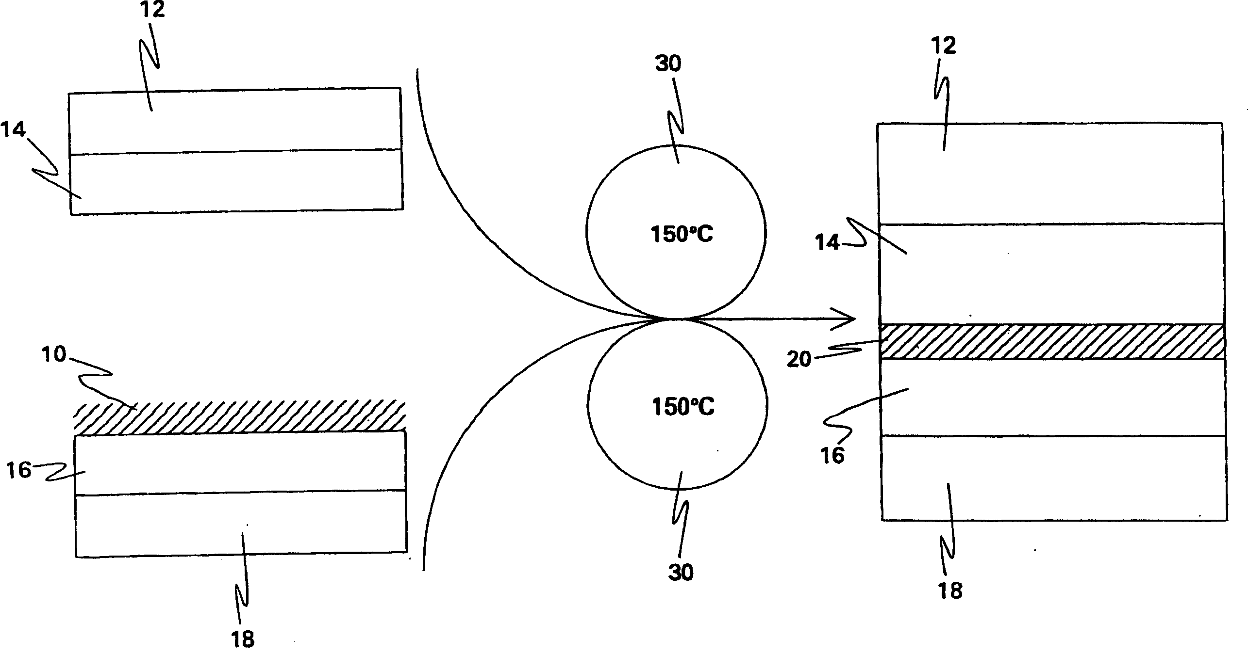
图1是本发明的一个实施方式的图示,表示通过至少一层使用助粘剂的表面处理下在电活化装置的两个电活化有机层之间的助粘作用。Figure 1 is a schematic representation of one embodiment of the present invention showing adhesion promotion between two electroactive organic layers of an electroactive device with at least one layer of surface treatment using an adhesion promoter.
图2是本发明的另一实施方式的图示,表示通过至少一层使用助粘剂的表面处理下在电活化装置的一个电活化有机层和一个金属电极层之间的助粘作用。Figure 2 is a schematic representation of another embodiment of the present invention showing adhesion promotion between an electroactive organic layer and a metal electrode layer of an electroactive device with at least one layer of surface treatment using an adhesion promoter.
图3是本发明的一个实施方式的图示,表示通过助粘剂和至少一个所述层的共沉积作用下电活化装置的两个电活化有机层之间的助粘作用。Figure 3 is a schematic representation of an embodiment of the invention showing adhesion promotion between two electroactive organic layers of an electroactive device by co-deposition of an adhesion promoter and at least one of said layers.
图4是本发明另一实施方式的图示,表示通过助粘剂和至少一个所述层的共沉积作用下电活化装置的一个电活化有机层和一个金属电极层之间的助粘作用。Figure 4 is a schematic representation of another embodiment of the invention showing adhesion promotion between an electroactive organic layer and a metal electrode layer of an electroactive device by co-deposition of an adhesion promoter and at least one of said layers.
发明详述Detailed description of the invention
在下面的说明和权利要求书中,将参考多个具有下面定义的术语。单数形式“一个”、“一种”和“该”包括复数指示含义,除非文中明确另外说明。在此使用的术语“电活化”是指下列材料(1)能够传输、阻断或储存电荷(正电荷或负电荷)的材料;(2)发光的,通常尽管不一定是荧光的,和/或(3)有效地光诱导性电荷产生作用。“电活化装置”是包含电活化材料的装置。在本文中电活化层是电活化装置的层,它包含至少一种电活化有机材料或者至少一种金属电极材料。在此使用的术语“聚合物”可以是指得自基本上单一单体的均聚物或者得自至少两种单体的共聚物,或者均聚物和共聚物两者。In the following description and claims, reference will be made to a number of terms having the following definitions. The singular forms "a", "an" and "the" include plural referents unless the context clearly dictates otherwise. As used herein, the term "electroactive" refers to a material that is (1) capable of transporting, blocking, or storing electrical charges (positive or negative); (2) luminescent, often though not necessarily fluorescent, and/or or (3) effective photo-induced charge generation. An "electroactive device" is a device comprising an electroactive material. An electroactive layer in this context is a layer of an electroactive device which comprises at least one electroactive organic material or at least one metallic electrode material. As used herein, the term "polymer" may refer to a homopolymer derived from substantially a single monomer or a copolymer derived from at least two monomers, or both homopolymers and copolymers.
本发明的多个实施方式中使用的术语“烷基”是指含有碳和氢原子的直链烷基、支链烷基、芳烷基、环烷基、双环烷基、三环烷基和多环烷基,并且其中除了碳和氢以外还任选含有例如选自周期表的第15、16和17族的原子。烷基可以是饱和或不饱和的,并且可以含有例如乙烯基或烯丙基。术语“烷基”还包括醇化基团的烷基部分。除非另外说明,在许多实施方式中正常和支链烷基是那些含有1-约32个碳原子的烷基,并且作为非限定实例包括C1-C32烷基(任选被一个或多个选自C1-C32烷基、C3-C15环烷基和芳基取代);和任选被一个或多个选自C1-C32烷基或芳基取代的C3-C15环烷基。某些非限定实例包括甲基、乙基、正丙基、异丙基、正丁基、仲丁基、叔丁基、戊基、新戊基、己基、庚基、辛基、壬基、癸基、十一烷基和十二烷基。环烷基和二环烷基的一些具体非限定实例包括环丁基、环戊基、环己基、甲基环己基、环庚基、二环庚基和金刚烷基。在许多实施方式中芳烷基包括那些含有7-约14个碳原子的芳烷基;这些包括,但不限于,苄基、苯基丁基、苯基丙基和苯基乙基。在本发明的许多实施方式中使用的术语“芳基”是指取代或未取代的含有6-20个环碳原子的芳基。芳基的一些非限定实例包括选择性被一个或多个选自C1-C32烷基、C3-C15环烷基、芳基和含有选自周期表的第15、16和17族的原子的官能团的基团取代的C6-C20芳基。芳基的一些具体非限定实例包括取代和未取代苯基、联苯基、甲苯基、二甲苯基、萘基和联萘基。The term "alkyl" used in various embodiments of the present invention refers to straight chain alkyl, branched chain alkyl, aralkyl, cycloalkyl, bicycloalkyl, tricycloalkyl and Polycyclic alkyl groups, and which optionally contain, for example, atoms selected from
本发明的一个方面是一种制备电活化装置中第一层的方法,包括步骤(i)通过混合至少一种助粘剂材料和至少一种电活化材料制备第一层组合物;(ii)是该第一层的组合物沉积在该电活化装置的第二电活化层上形成该第一层,其中该第一层组合物确保第一层和第二层之间粘合。在另一实施方式中电活化装置进一步包括电活化材料的第三层,该第三层与第一层相邻并接触且该第一层位于所述第二层和第三层之间。在一具体实施方式中该方法任选进一步包括使该第三层沉积在第一层的与第二层相反的表面上的步骤,其中该第一层组合物确保该第一层和第二层之间或第一层和第三层之间、或第一层与第二层和第三层两者之间粘合。任何层的沉积可以任选在至少一个加热处理步骤之后进行。One aspect of the present invention is a method of making a first layer in an electroactive device comprising the steps of (i) preparing a first layer composition by mixing at least one adhesion promoter material and at least one electroactive material; (ii) The composition of the first layer is deposited on the second electroactive layer of the electroactive device to form the first layer, wherein the first layer composition ensures adhesion between the first layer and the second layer. In another embodiment the electro-active device further comprises a third layer of electro-active material adjacent to and in contact with the first layer and the first layer is located between said second and third layers. In one embodiment the method optionally further comprises the step of depositing the third layer on the surface of the first layer opposite the second layer, wherein the first layer composition ensures that the first layer and the second layer between the first layer and the third layer, or between the first layer and the second layer and the third layer. Deposition of any layers may optionally be followed by at least one heat treatment step.
本发明的另一方面是一种确保或改进电活化装置的两层之间的粘合作用的方法,该方法包括使至少一种助粘剂材料沉积在至少一个电活化有机层或金属电极层的表面上的步骤。该方法通常包括使含有至少一种助粘剂材料的表面处理组合物沉积在至少一个电活化有机层的至少一个表面上或在至少一个金属电极层的一个表面上的步骤。第二电活化层随后可以沉积在该助粘剂上,由此该助粘剂确保该第二层与助粘剂所沉积的层之间发生粘合。在一具体实施方式中含有至少一种助粘剂材料的表面处理组合物沉积在一电活化层的一个表面上或者在一金属电极层的一个表面上。在另一具体实施方式中含有至少一种助粘剂材料的表面处理组合物沉积在至少两个电活化有机层的一个表面上或者一个电活化有机层的一个表面和一个金属电极层的一个表面上。一个以上的电活化层可以用助粘剂材料处理,其中该助粘剂材料可以相同或不同。任何层或表面处理组合物的沉积可以任选在至少一个热处理步骤后进行。Another aspect of the invention is a method of ensuring or improving adhesion between two layers of an electroactive device, the method comprising depositing at least one adhesion promoter material on at least one electroactive organic layer or metal electrode layer steps on the surface. The method generally includes the step of depositing a surface treatment composition comprising at least one adhesion promoter material on at least one surface of at least one electroactive organic layer or on a surface of at least one metal electrode layer. A second electroactive layer can then be deposited on the adhesion promoter, whereby the adhesion promoter ensures adhesion between the second layer and the layer on which the adhesion promoter was deposited. In one embodiment a surface treatment composition comprising at least one adhesion promoter material is deposited on a surface of an electroactive layer or on a surface of a metal electrode layer. In another embodiment a surface treatment composition comprising at least one adhesion promoter material is deposited on one surface of at least two electroactive organic layers or one surface of one electroactive organic layer and one surface of a metal electrode layer superior. More than one electroactive layer may be treated with an adhesion promoter material, where the adhesion promoter materials may be the same or different. Deposition of any layer or surface treatment composition may optionally be followed by at least one heat treatment step.
助粘剂材料包括例如,但不限于,金属化合物或9,9-二取代的芴基化合物。所述金属化合物包括至少一个选自乙酰氧基、乙酰基丙酮酸盐、丙烯酰氧基、烷氧基、氨基丙基、甲醇、羧酸盐、硅烷醇、甲硅烷氧基、亚磷酸盐、磷酸盐、缩水甘油氧基、巯基丙基、卤化物、氯化物、溴化物和氧化物的部分;其中该金属选自硅、锡、锆、铪、铝、锑和钛。金属化合物的实例包括四烷醇化钛,四丁醇化钛,四丙醇化钛,原硅酸四烷基酯,原硅酸四乙酯,四烷醇化锆等化合物及其组合物。Adhesion promoter materials include, for example, but are not limited to, metal compounds or 9,9-disubstituted fluorenyl compounds. The metal compound comprises at least one selected from the group consisting of acetoxy, acetylacetonate, acryloxy, alkoxy, aminopropyl, methanol, carboxylate, silanol, siloxy, phosphite, Moieties of phosphate, glycidyloxy, mercaptopropyl, halide, chloride, bromide and oxide; wherein the metal is selected from the group consisting of silicon, tin, zirconium, hafnium, aluminum, antimony and titanium. Examples of metal compounds include compounds such as titanium tetraalkoxide, titanium tetrabutoxide, titanium tetrapropoxide, tetraalkyl orthosilicate, tetraethyl orthosilicate, zirconium tetraalkoxide, and combinations thereof.
助粘剂的其他实例包括例如,但不限于,α-(1-萘基)-ω-三烷氧基甲硅烷基烷烃类。本发明的一个方面中助粘剂材料是1-(1-萘基)-2-三烷氧基甲硅烷基乙烷,其实例包括1-(1-萘基)-2-三乙氧基甲硅烷基乙烷(NTES),等化合物。此类α-(1-萘基)-ω-三烷氧基甲硅烷基烷烃类的代表性实例全面公开在本申请人的共同待决的系列申请10/761,696,2004年1月20日提交。Other examples of adhesion promoters include, for example, but not limited to, α-(1-naphthyl)-ω-trialkoxysilylalkanes. In one aspect of the invention the adhesion promoter material is 1-(1-naphthyl)-2-trialkoxysilylethane, examples of which include 1-(1-naphthyl)-2-triethoxy Silylethane (NTES), and other compounds. Representative examples of such α-(1-naphthyl)-ω-trialkoxysilylalkanes are fully disclosed in applicant's co-pending
助粘剂材料的其他实例包括选择性与烯基芳族化合物(例如但不限于苯乙烯)共聚的乙烯基萘聚合物。本发明的另一方面中所述助粘剂是苯乙烯和乙烯基萘的共聚物(NAPHSTYR),其中苯乙烯(x)与乙烯基萘(1-x)的比例为x∶1-x,其中x可以从0-约0.6变化。此类共聚物的代表性实例一般性公开在本申请人的共同待决申请中,(GE Docket号148981)。NAPHSTYR的重均分子量在一实施方式中在约8000-约75000的范围内,在另一实施方式中为约12000-约65000的范围内,并且在另一实施方式中在约45000-约65000的范围内。NAPHSTYR的数均分子量(Mn)在一实施方式中在约4000-约30000的范围内,在另一实施方式中在约8000-约28000的范围内,并且在另一实施方式中在约14000-约26000的范围内。在一特定实施方式中NAPHSTYR的Mw值为约50000-约60000的范围内,并且Mn值在约18000-约24000的范围内。Other examples of adhesion promoter materials include vinyl naphthalene polymers selectively copolymerized with alkenyl aromatic compounds such as, but not limited to, styrene. In another aspect of the present invention, the adhesion promoter is a copolymer of styrene and vinylnaphthalene (NAPHSTYR), wherein the ratio of styrene (x) to vinylnaphthalene (1-x) is x: 1-x, where x can vary from 0 to about 0.6. Representative examples of such copolymers are generally disclosed in the applicant's co-pending application, (GE Docket No. 148981). The weight average molecular weight of NAPHSTYR is in the range of about 8000 to about 75000 in one embodiment, in the range of about 12000 to about 65000 in another embodiment, and in the range of about 45000 to about 65000 in another embodiment within range. The number average molecular weight (Mn) of NAPHSTYR is in the range of about 4000 to about 30000 in one embodiment, in the range of about 8000 to about 28000 in another embodiment, and in another embodiment in the range of about 14000 to In the range of about 26000. In a particular embodiment NAPHSTYR has a Mw value in the range of about 50,000 to about 60,000 and a Mn value in the range of about 18,000 to about 24,000.
适当助粘剂的其他实例包括例如,但不限于,甲基丙烯酰氧基烷基三烷氧基硅烷类,其实例包括,但不限于,甲基丙烯酰氧基丙基三甲氧基硅烷(MAPTMS)等化合物。适当助粘剂的其他实例包括例如,但不限于,缩水甘油氧基烷基三烷氧基硅烷类,其实例包括,但不限于,3-缩水甘油氧基丙基三烷氧基硅烷等化合物。在一特定实施方式中适当缩水甘油氧基烷基三烷氧基硅烷类包括3-缩水甘油氧基丙基三甲氧基硅烷(GLYMO)。Other examples of suitable adhesion promoters include, for example, but are not limited to, methacryloxyalkyltrialkoxysilanes, examples of which include, but are not limited to, methacryloxypropyltrimethoxysilane ( MAPTMS) and other compounds. Other examples of suitable adhesion promoters include compounds such as, but not limited to, glycidoxyalkyltrialkoxysilanes, examples of which include, but are not limited to, 3-glycidoxypropyltrialkoxysilane . Suitable glycidoxyalkyltrialkoxysilanes in a particular embodiment include 3-glycidoxypropyltrimethoxysilane (GLYMO).
沉积的方法包括自旋涂层法,浸涂法,逆旋涂层法,绕丝式或Mayer杆式涂法,直接和偏移凹版涂法(direct and offset gravurecoating),槽沟压铸模涂法(slot die coating),叶片涂法,热融涂法,帘幕式涂法,刮旋涂法,挤出法,气刮涂法,喷涂法,旋转筛涂法,多层滑片涂法,共挤出法,半月涂法,逗号和微照像凹版涂法,平版法,朗谬尔法和闪式蒸发,蒸气沉积法,等离子体加速化学-蒸气沉积法(“PECVD”),射频等离子体加速化学-蒸气沉积法(“RFPECVD”),扩展式热等离子体化学-蒸气沉积法(“ETPCVD”),溅射法包括,但不限于,反应性溅射法,电子-回旋加速器-共振等离子体加速化学-蒸气沉积法(“ECRPECVD”),电感耦合等离子体甲酸化学-蒸气沉积法(“ICPECVD”),等技术,和它们的组合。Deposition methods include spin coating, dip coating, reverse spin coating, wire wound or Mayer rod coating, direct and offset gravure coating, groove die coating (slot die coating), blade coating method, hot melt coating method, curtain coating method, scrape spin coating method, extrusion method, air scrape coating method, spray coating method, rotary screen coating method, multi-layer slide coating method, Co-extrusion, half-moon coating, comma and gravure coating, lithography, Langmuir and flash evaporation, vapor deposition, plasma accelerated chemical-vapor deposition (“PECVD”), radio frequency plasma Bulk accelerated chemical-vapor deposition (“RFPECVD”), extended thermal plasma chemical-vapor deposition (“ETPCVD”), sputtering methods including, but not limited to, reactive sputtering, electron-cyclotron-resonance Plasma Accelerated Chemical-Vapor Deposition ("ECRPECVD"), Inductively Coupled Plasma Formic Acid Chemical-Vapor Deposition ("ICPECVD"), and other techniques, and combinations thereof.
例如在自旋涂法中,根据旋转器的参数,例如但不限于,含有电活化材料或助粘剂或两者的溶液或分散体中的固体的速度、百分比可以变化,从而得到所需厚度。所需厚度则一般可能依赖于电活化材料和助粘剂之一或两者以及其他存在的固体的化学和材料性质,并且本领域技术人员无需过度实验就可以很容易地测定。在一具体实施方式中在沉积的溶液或分散体中的电活化材料或助粘剂或两者的浓度可以在约0.01%固体-约10%固体的范围内变化,并且在另一特定书实施方式中是在约0.5%固体-约3%固体的范围内。For example in a spin coating process, depending on the parameters of the spinner, such as but not limited to, the velocity, percentage of solids in a solution or dispersion containing electroactive material or adhesion promoter or both can be varied to obtain the desired thickness . The desired thickness then generally may depend on the chemical and material properties of one or both of the electroactive material and adhesion promoter, and other solids present, and can be readily determined by one skilled in the art without undue experimentation. The concentration of electroactive material or adhesion promoter or both in the deposited solution or dispersion may vary from about 0.01% solids to about 10% solids in one embodiment, and in another embodiment Moderately is in the range of about 0.5% solids to about 3% solids.
本发明的另一方面是含有至少一种助粘剂和至少一种电活化材料的致密混合物的电活化装置的层。在本文中该致密混合物得自该层沉积之前的溶液或分散体中助粘剂和电活化材料的混合物。本发明的另一方面是通过一种方法制备的电活化装置的一层,该方法包括步骤(i)通过混合至少一种助粘剂材料和至少一种电活化材料制备第一层组合物,和(ii)使第一层的组合物沉积在该电活化装置的第二层电活化层上,其中第一层组合物使得第一层和第二层之间粘合。本发明的另一方面在于一种包括一层含有至少一种助粘剂和至少一种电活化有机材料的致密混合物的电活化装置。本发明的另一方面是通过所述方法制备的第一层组合物,该方法包括步骤(i)通过混合至少一种助粘剂材料和至少一种电活化材料制备第一层组合物,和(ii)使第一层的组合物沉积在该电活化装置的第二层电活化层上,其中第一层组合物使得第一层和第二层之间粘合。Another aspect of the invention is a layer of an electroactive device comprising an intimate mixture of at least one adhesion promoter and at least one electroactive material. The dense mixture here results from the mixture of adhesion promoter and electroactive material in solution or dispersion prior to deposition of the layer. Another aspect of the invention is a layer of an electroactive device prepared by a method comprising the step (i) of preparing a first layer composition by mixing at least one adhesion promoter material and at least one electroactive material, and (ii) depositing a first layer composition on the second electroactive layer of the electroactive device, wherein the first layer composition provides adhesion between the first layer and the second layer. Another aspect of the invention resides in an electroactive device comprising a layer of an intimate mixture comprising at least one adhesion promoter and at least one electroactive organic material. Another aspect of the invention is a first layer composition prepared by the method comprising the steps of (i) preparing a first layer composition by mixing at least one adhesion promoter material and at least one electroactive material, and (ii) depositing the composition of the first layer on the second electroactive layer of the electroactive device, wherein the composition of the first layer provides adhesion between the first layer and the second layer.
本发明的另一方面是通过一种方法制备的电活化装置的一层,该方法包括使至少一种助粘剂材料沉积在电活化层的表面上的步骤。本发明的另一方面在于一种包括通过所述方法制备的一层的电活化装置,该方法包括使至少一种助粘剂材料沉积在电活化层的表面上的步骤。在一实施方式中该助粘剂的表面厚度是约1纳米-约100纳米之间。在本发明的另一实施方式中,助粘剂的表面厚度为约1纳米-约10纳米。Another aspect of the invention is a layer of an electroactive device prepared by a method comprising the step of depositing at least one adhesion promoter material on the surface of the electroactive layer. Another aspect of the invention resides in an electroactive device comprising a layer prepared by the method comprising the step of depositing at least one adhesion promoter material on the surface of the electroactive layer. In one embodiment, the surface thickness of the adhesion promoter is between about 1 nanometer and about 100 nanometers. In another embodiment of the present invention, the surface thickness of the adhesion promoter is from about 1 nanometer to about 10 nanometers.
在某些特定实施方式中所述电活化装置的电活化层材料选自电极材料,发光材料,吸光材料,电荷传输材料,电荷注入材料,电荷阻断材料及其组合。在某些特定实施方式中,所述电活化装置选自发光装置,有机发光装置,光电材料,光电导体,光检测器,液晶显示器,有机晶体管或其他分子电子装置部件,和其组合。In some specific embodiments, the electroactive layer material of the electroactive device is selected from electrode materials, light emitting materials, light absorbing materials, charge transport materials, charge injection materials, charge blocking materials and combinations thereof. In certain specific embodiments, the electroactive device is selected from light emitting devices, organic light emitting devices, optoelectronic materials, photoconductors, photodetectors, liquid crystal displays, organic transistors or other molecular electronic device components, and combinations thereof.
在本发明的一个实施方式中电活化装置一般包括:(a)阳极;(b)阴极;和(c)空穴阻断层。在另一实施方式中该电活化装置一般包括:(a)阳极;(b)发光层;(c)空穴阻断层;和(d)阴极。在另一实施方式中该电活化装置常常包括:(i)基片;(ii)在基片上形成的阳极;(iii)在该阳极上形成的导体聚合物或空穴传输材料层;(iv)任选电子阻断层;(v)发光材料层;(vi)空穴阻断材料层,(vii)电子传输材料层;和(viii)在电子传输材料层上形成的阴极。在另一实施方式中,该电活化装置一般包括:(a)阳极;(b)阴极;和(c)发光材料层;在某些其它实施方式中,该电活化装置一般包括:(a)基片;(b)在基片上形成的阳极;(c)在该阳极上形成的导体聚合物和空穴传输材料层;(d)任选电子阻断层;(f)发光材料层;(g)任选的含有空穴阻断材料的层;(h)任选的含有电子传输材料的层;和(i)阴极。在本发明的一实施方式中,具有吸光层的电活化装置一般包括:(a)阳极;(b)阴极和(c)吸光材料层。本发明的电活化装置可以包括附加层例如,但不限于,一个或多个耐磨层,化学抗性层,光致发光层,辐射吸收层,辐射反射层,屏蔽层,平面化层,和其组合。In one embodiment of the invention an electroactive device generally comprises: (a) an anode; (b) a cathode; and (c) a hole blocking layer. In another embodiment the electroactive device generally comprises: (a) an anode; (b) a light emitting layer; (c) a hole blocking layer; and (d) a cathode. In another embodiment the electroactive device often comprises: (i) a substrate; (ii) an anode formed on the substrate; (iii) a layer of conductive polymer or hole transport material formed on the anode; (iv) ) optionally an electron blocking layer; (v) a light emitting material layer; (vi) a hole blocking material layer, (vii) an electron transporting material layer; and (viii) a cathode formed on the electron transporting material layer. In another embodiment, the electroactive device generally includes: (a) an anode; (b) a cathode; and (c) a layer of emissive material; in certain other embodiments, the electroactive device generally includes: (a) A substrate; (b) an anode formed on the substrate; (c) a conductive polymer and a hole transport material layer formed on the anode; (d) an optional electron blocking layer; (f) a light emitting material layer; ( g) an optional layer comprising a hole blocking material; (h) an optional layer comprising an electron transport material; and (i) a cathode. In one embodiment of the present invention, an electroactive device having a light absorbing layer generally includes: (a) an anode; (b) a cathode and (c) a layer of light absorbing material. The electroactive devices of the present invention may include additional layers such as, but not limited to, one or more abrasion resistant layers, chemically resistant layers, photoluminescent layers, radiation absorbing layers, radiation reflecting layers, shielding layers, planarizing layers, and its combination.
发光材料的非限定实例包括聚(N-乙烯基咔唑)及其衍生物;聚芴及其衍生物例如聚(烷基芴),例如聚(9,9-二己基芴),聚(二辛基芴)或聚{9,9-二(3,6-二氧杂庚基)-芴-2,7-二基};聚(对-亚苯基)及其衍生物例如聚(2-癸氧基-1,4-亚苯基)或聚(2,5-二庚基-1,4-亚苯基);聚(对亚苯基亚乙烯基)(“PPV”)及其衍生物例如二烷氧基取代的PPV和氰基取代的PPV;聚噻吩及其衍生物例如聚(3-烷基噻吩),聚(4,4’-二烷基-2,2’-联噻吩),聚(2,5-亚噻酚基亚乙烯基);聚(吡啶亚乙烯基)及其衍生物;聚喹喔啉及其衍生物;和聚喹啉及其衍生物。这些聚合物的混合物,或基于一种或多种这些聚合物和其他的共聚物可以用来改变发光的颜色。Non-limiting examples of luminescent materials include poly(N-vinylcarbazole) and its derivatives; polyfluorene and its derivatives such as poly(alkylfluorene), such as poly(9,9-dihexylfluorene), poly(di octylfluorene) or poly{9,9-bis(3,6-dioxaheptyl)-fluorene-2,7-diyl}; poly(p-phenylene) and its derivatives such as poly(2 -decyloxy-1,4-phenylene) or poly(2,5-diheptyl-1,4-phenylene); poly(p-phenylenevinylene) (“PPV”) and its Derivatives such as dialkoxy-substituted PPV and cyano-substituted PPV; polythiophene and its derivatives such as poly(3-alkylthiophene), poly(4,4'-dialkyl-2,2'-bi Thiophene), poly(2,5-thienylvinylene); poly(pyridylvinylene) and its derivatives; polyquinoxaline and its derivatives; and polyquinoline and its derivatives. Mixtures of these polymers, or copolymers based on one or more of these polymers and others can be used to change the color of the emission.
另一类适当的发光聚合物材料是聚硅烷类。通常,聚硅烷是被多种烷基和/或芳基侧基取代的直链硅主链聚合物。它们是准一维材料并且沿着聚合物主链具有离域sigma-共轭电子。聚硅烷的实例包括聚(二-正丁基硅烷),聚(二-正戊基硅烷,聚(二-正己基硅烷),聚(甲基苯基硅烷),和聚{双(对丁基苯基)硅烷}。Another class of suitable light emitting polymer materials are polysilanes. Typically, polysilanes are linear silicon backbone polymers substituted with various alkyl and/or aryl side groups. They are quasi-one-dimensional materials and have delocalized sigma-conjugated electrons along the polymer backbone. Examples of polysilanes include poly(di-n-butylsilane), poly(di-n-pentylsilane, poly(di-n-hexylsilane), poly(methylphenylsilane), and poly{bis(p-butyl phenyl)silane}.
具有分子量小于例如约5000的由大量分子单元组成的有机材料也常常用作发光材料。此类材料的实例为1,3,5-三{n-(4-二苯基氨基苯基)苯基氨基}苯。有机发光材料也可以是由低分子量有机分子制成,例如苯基蒽,四芳基乙烯,香豆素,红荧烯,四苯基丁二烯,蒽,茉,蔻,或其衍生物。其他适当的材料是低分子量金属有机复合物例如乙酰基丙酮酸铝,乙酰基丙酮酸镓,乙酰基丙酮酸铟,(吡啶甲基甲基酮)-二{2,6-二(叔丁基)酚}铝,(4-甲氧基-吡啶甲基甲基酮)-二(乙酰基丙酮酸)钪,及其混合物。其他有机发射性材料包括选自8-羟基喹啉的有机金属复合物的材料。Organic materials composed of a large number of molecular units having a molecular weight of less than, for example, about 5000 are also frequently used as light-emitting materials. An example of such a material is 1,3,5-tris{n-(4-diphenylaminophenyl)phenylamino}benzene. Organic light-emitting materials can also be made of low molecular weight organic molecules, such as phenylanthracene, tetraarylethene, coumarin, rubrene, tetraphenylbutadiene, anthracene, moss, corone, or their derivatives. Other suitable materials are low molecular weight metal-organic compounds such as aluminum acetylacetonate, gallium acetylacetonate, indium acetylacetonate, (picolylmethyl ketone)-bis{2,6-bis(tert-butyl ) aluminum phenoxide, (4-methoxy-pyridylmethyl ketone)-scandium bis(acetylacetonate), and mixtures thereof. Other organic emissive materials include materials selected from organometallic complexes of 8-hydroxyquinoline.
可以使用的LEP聚合物溶剂的实例包括芳香混合物,二甲苯类,甲苯,THF,氯苯,二氯苯等,及其组合。Examples of LEP polymer solvents that can be used include aromatic mixtures, xylenes, toluene, THF, chlorobenzene, dichlorobenzene, etc., and combinations thereof.
空穴注入增强材料的非限定实例是亚芳基化合物例如,但不限于,3,4,9,10-苝四甲酸二酐,二(1,2,5-噻二唑并)-对醌二(1,3-二硫醇),等。Non-limiting examples of hole injection enhancing materials are arylene compounds such as, but not limited to, 3,4,9,10-perylenetetracarboxylic dianhydride, bis(1,2,5-thiadiazolo)-p-quinone Bis(1,3-dithiol), etc.
空穴传输材料的实例包括三芳基二胺,四苯基二胺,芳香叔胺类,腙衍射,咔唑衍生物,三唑衍生物,咪唑衍生物,具有氨基的噁二唑衍生物,聚噻吩类,等等。Examples of hole transport materials include triaryldiamine, tetraphenyldiamine, aromatic tertiary amines, hydrazone diffraction, carbazole derivatives, triazole derivatives, imidazole derivatives, oxadiazole derivatives having amino groups, poly Thiophenes, etc.
适合电子注入的材料和传输增强材料包括金属有机复合物例如,但不限于,三(8-羟基喹啉)铝,噁二唑衍生物,苝衍生物,吡啶衍生物,嘧啶衍生物,喹啉衍生物,喹唑啉衍生物,二苯基醌衍生物,硝基取代的芴衍生物,等等。Materials suitable for electron injection and transport enhancing materials include metal-organic compounds such as, but not limited to, tris(8-quinolinolato)aluminum, oxadiazole derivatives, perylene derivatives, pyridine derivatives, pyrimidine derivatives, quinoline Derivatives, quinazoline derivatives, diphenylquinone derivatives, nitro-substituted fluorene derivatives, etc.
空穴注入和传输材料的非限定实例包括有机聚合物,例如,但不限于,聚(3,4-亚乙基二氧基噻吩)(“PEDOT”),聚苯胺,等等。Non-limiting examples of hole injection and transport materials include organic polymers such as, but not limited to, poly(3,4-ethylenedioxythiophene) ("PEDOT"), polyaniline, and the like.
空穴阻断层的适当材料包括聚(N-乙酰基咔唑),浴铜灵(“BCP”),二(2-甲基-8-羟基喹啉)三苯基硅烷酸化铝(III),二(2-甲基-8-羟基喹啉)4-酚酸铝(III),二(2-甲基-8-羟基喹啉)4-苯基酚酸铝(III),等。Suitable materials for the hole blocking layer include poly(N-acetylcarbazole), bathocuproine ("BCP"), aluminum(III) bis(2-methyl-8-hydroxyquinoline)triphenylsilane , bis(2-methyl-8-hydroxyquinoline) 4-phenolic acid aluminum (III), bis(2-methyl-8-hydroxyquinoline) 4-phenylphenolic acid aluminum (III), etc.
电活化装置的适当阴极层材料一般包括具有低自有能值的材料。阴极材料的非限定实例例如,但不限于K,Li,Na,Mg,Ca,Sr,Ba,Al,Ag,Au,In,Sn,Zn,Zr,Sc,Y,Mn,Pb,镧系的元素,其合金,特别是Ag-Mg合金,Al-Li合金,In-Mg合金,Al-Ca合金,和Li-Al合金,及其混合物。阴极材料的其他实例可以包括碱金属氟化物,或碱土金属氟化物,此类聚合物的混合物。其他阴极材料例如氧化铟锡,氧化锡,氧化铟,氧化锌,氧化铟锌,氧化锌铟锡,氧化锑,碳毫微管,并且其混合物也适宜。另外,阴极可以由两层组成以提高电子注射。实例包括,但不限于,LiF或NaF的内层,随后是铝或银的外层,或者钙的内层,随后是铝或银的外层。Suitable cathode layer materials for electroactive devices generally include materials with low intrinsic energy values. Non-limiting examples of cathode materials such as, but not limited to, K, Li, Na, Mg, Ca, Sr, Ba, Al, Ag, Au, In, Sn, Zn, Zr, Sc, Y, Mn, Pb, lanthanides Elements, alloys thereof, especially Ag-Mg alloys, Al-Li alloys, In-Mg alloys, Al-Ca alloys, and Li-Al alloys, and mixtures thereof. Other examples of cathode materials may include alkali metal fluorides, or alkaline earth metal fluorides, mixtures of such polymers. Other cathode materials such as indium tin oxide, tin oxide, indium oxide, zinc oxide, indium zinc oxide, zinc indium tin oxide, antimony oxide, carbon nanotubes, and mixtures thereof are also suitable. Additionally, the cathode can consist of two layers to enhance electron injection. Examples include, but are not limited to, an inner layer of LiF or NaF followed by an outer layer of aluminum or silver, or an inner layer of calcium followed by an outer layer of aluminum or silver.
适合电活化装置的阳极材料一般包括具有锆自有能值的材料。阳极材料的实例包括,但不限于,氧化铟锡(ITO),氧化锡,氧化铟,氧化锌,氧化铟锌,镍,金,及其混合物。Anode materials suitable for electro-active devices generally include materials having an intrinsic energy value of zirconium. Examples of anode materials include, but are not limited to, indium tin oxide (ITO), tin oxide, indium oxide, zinc oxide, indium zinc oxide, nickel, gold, and mixtures thereof.
在本发明的另一实施方式中包括式(I)的9,9-二取代芴基化合物:In another embodiment of the present invention include 9,9-disubstituted fluorenyl compounds of formula (I):
其中R独立地是烷基,芳基,卤素,氰基,醇化物,羧酸酯,或羟基;各“x”独立地具有0至芳环上可以被取代位置的数目的值;各R1独立地是C1-C16烷基或芳基;各R2独立地是C1-C16烷基。应注意虽然表示出式(I)中双键的特定几何学,但对两个双键的几何学没有限定作用。有关两个双键各自的几何学可以独立地是顺式或反式。在某些具体实施方式中x为0;各R1相同并且是C1-C16烷基;和各R2相同。在其他具体实施方式中x是0;各R1相同且选自甲基、乙基和正丙基;和各R2相同且选自甲基、乙基、正丙基、异丙基、正丁基、仲丁基、正戊基、异戊基、甲基戊基、正己基,和异己基。wherein R is independently alkyl, aryl, halogen, cyano, alcoholate, carboxylate, or hydroxy; each "x" independently has a value from 0 to the number of positions that can be substituted on the aromatic ring; each R 1 are independently C 1 -C 16 alkyl or aryl; each R 2 is independently C 1 -C 16 alkyl. It should be noted that while the specific geometry of the double bond in formula (I) is shown, there is no limitation on the geometry of the two double bonds. The respective geometries regarding the two double bonds can be independently cis or trans. In certain embodiments x is 0; each R 1 is the same and is C 1 -C 16 alkyl; and each R 2 is the same. In other specific embodiments x is 0; each R is the same and is selected from methyl, ethyl, and n-propyl; and each R is the same and is selected from methyl, ethyl, n-propyl, isopropyl, n-butyl base, sec-butyl, n-pentyl, isopentyl, methylpentyl, n-hexyl, and isohexyl.
在另一实施方式中本发明包括制备式(I)的9,9-二取代芴基化合物的方法。在一示例方法中式(I)的9,9-二取代芴基化合物在第一步中在反应条件下在偶极非质子溶剂中与碱和式(III)的带有可置换基团的取代炔烃接触:In another embodiment the present invention includes a process for the preparation of 9,9-disubstituted fluorenyl compounds of formula (I). In an exemplary process, a 9,9-disubstituted fluorenyl compound of formula (I) is substituted in a first step with a base and a displaceable group of formula (III) under reaction conditions in a dipolar aprotic solvent. Alkyne exposure:

其中R,x和R2如上所述,并且Z是可置换基团。在某些实施方式中Z选自卤化物,溴化物,和氯化物。偶极非质子溶剂实例包括,但不限于,二甲基亚砜,二甲基乙酰胺等。在示例方法中式(II)的9,9-未取代芴基化合物在第一步中反应条件下在非极性溶剂中与碱、相转移催化剂和式(III)的带有可置换基团的取代烯烃接触。实例非极性溶剂包括,但不限于,甲苯,二甲苯,氯苯等。反应条件包括温度、浓度、时间的有效值和适合以所需收率提供所需化合物的变量。可以使用任何有效的碱。在某些实施方式中有效的碱包括碱金属氢氧化物例如氢氧化钠,并且通常为氢氧化钠水溶液。可以使用任何有效的相转移催化剂。在某些实施方式中,有效的相转移催化剂包括季铵盐,例如四烷基卤化铵。本领域技术人员可以很容易地测定相转移催化剂的量而无需过度实验。碱和烯烃化合物(III)的量一般至少分别是9,9-未取代芴基化合物的量的至少2当量。where R, x and R2 are as described above, and Z is a displaceable group. In certain embodiments Z is selected from halides, bromides, and chlorides. Examples of dipolar aprotic solvents include, but are not limited to, dimethylsulfoxide, dimethylacetamide, and the like. In the exemplary method, the 9,9-unsubstituted fluorenyl compound of formula (II) is in a non-polar solvent under the reaction conditions in the first step with a base, a phase transfer catalyst and a compound with a displaceable group of formula (III). Substituted olefin contacts. Example non-polar solvents include, but are not limited to, toluene, xylene, chlorobenzene, and the like. Reaction conditions include effective values for temperature, concentration, time and variables as appropriate to provide the desired compound in the desired yield. Any effective base can be used. Bases useful in certain embodiments include alkali metal hydroxides such as sodium hydroxide, and typically aqueous sodium hydroxide. Any effective phase transfer catalyst can be used. In certain embodiments, effective phase transfer catalysts include quaternary ammonium salts, such as tetraalkylammonium halides. The amount of phase transfer catalyst can be readily determined by one skilled in the art without undue experimentation. The amounts of the base and the olefinic compound (III) are generally at least 2 equivalents to the amount of the 9,9-unsubstituted fluorenyl compound, respectively.
第一步的产物是式(IV)的9,9-二(炔基)芴基化合物:The product of the first step is a 9,9-di(alkynyl)fluorenyl compound of formula (IV):
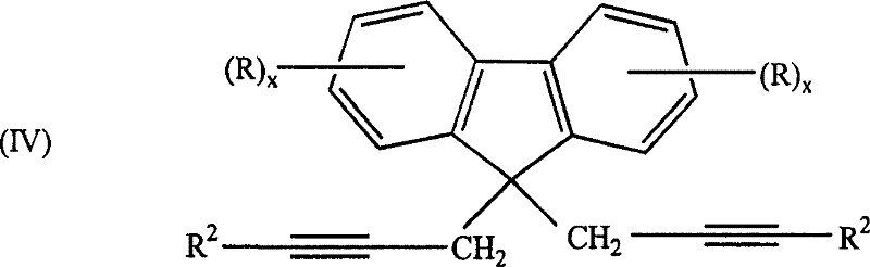
其中R,x和R2如上所述,并且Z是可置换基团。式(IV)的9,9-二(炔基)芴基化合物可以从该步骤1的反应中分离出来并且利用有效方法纯化,或者,如果需要,使用分离或未分离的粗产物。where R, x and R2 are as described above, and Z is a displaceable group. The 9,9-bis(alkynyl)fluorenyl compound of formula (IV) can be isolated from the reaction of this step 1 and purified using efficient methods, or, if desired, the crude product, isolated or not isolated, is used.
在例举方法的典型第二步中,式(IV)的9,9-二(炔基)芴基化合物用有效硅氢化试剂在有效硅氢化催化剂的存在下硅氢化。典型的有效硅氢化试剂含有-Si-H部分并且在许多实施方式中具有式(R1O)3-Si-H,其中R1如上所述。有效硅氢化试剂是本领域熟知的且一般包括周期表的第8、9或10族的金属例如铂。在硅氢化反应中可以任选使用有效溶剂。在一具体实施方式中硅氢化反应在无溶剂条件下进行。所需式(I)的9,9-二取代芴基化合物可以从步骤2的反应中分离并利用任何有效方法纯化,或者,如果需要,使用分离或未分离的粗产物。In a typical second step of the exemplified process, a 9,9-bis(alkynyl)fluorenyl compound of formula (IV) is hydrosilated with an effective hydrosilation reagent in the presence of an effective hydrosilation catalyst. Typical effective hydrosilation reagents contain a -Si-H moiety and in many embodiments have the formula (R 1 O) 3 -Si-H, where R 1 is as described above. Effective hydrosilation agents are well known in the art and generally include metals of
无需进一步解释,本领域技术人员肯定可以根据本文的说明,最大程度地应用本发明。下列实施例为本领域技术人员实施本发明提供进一步的指导。下列实施例和阳极基片(18)包括在0.18毫米厚的聚(对苯二甲酸乙二酯)薄片上存在一导体氧化铟锡(ITO)的薄膜。阴极基片(12)包括在0.18毫米厚的聚(对苯二甲酸乙二酯)薄片上存在一铝的薄膜。Without further elaboration, it is believed that one skilled in the art can, based on the description herein, utilize the present invention to its fullest extent. The following examples provide further guidance to those skilled in the art in the practice of the present invention. The following example and anode substrate (18) consisted of a thin film of a conductor indium tin oxide (ITO) on a 0.18 mm thick polyethylene (ethylene terephthalate) sheet. The cathode substrate (12) consisted of a thin film of aluminum on a 0.18 mm thick poly(ethylene terephthalate) sheet.
实施例1Example 1
图1的实施方式中所例举的本实施例证实,通过用助粘剂表面处理两层中的至少一层可改进电活化装置的两个电活化有机层之间的粘合作用。含有PEDOT-PSS聚合物(水中含固体2.6%)的空穴传输层(16)以3000rpm自旋涂层在阳极基片(18)上并且在110℃下烘烤。对PEDOT-PSS层进行表面处理以改进对后续层的粘合作用。特别是,将含有式(I)的9,9-二取代芴基化合物,其中x为0,并且R1和R2两者为乙基,的溶液(对二甲苯中含约0.1%固体)以3000rpm的速度自旋涂层在PEDOT-PSS层的表面上并且将该新的阴极复合材料在110℃下烘烤。含有美国染料原329(ADS329)的发光聚合物(LEP)材料(14)自旋涂层在该阴极基片(12)上并在110℃下烘烤。阳极复合材料和阴极复合材料叠加并经过辊式层布贴合机在150℃下以1米/分钟的速度操作,如图1所示。向阳极和阴极部分施加7伏特以启动该装配的装置,得到一定量度的电流。测定亮度和电流并且与没有PEDOT-PSS表面处理结构的对照装置进行对比。数据显示,本发明的装置与参比装置相比电流相当或增强。LEP层和PEDOT-PSS层之间的结构粘合程度是通过撕开层压层来确定。与相同装配没有表面处理的层压复合层相比,LEP材料与PEDOT-PSS层的转移增加30%,表明本发明的方法提供了良好的结构粘合作用。This example, illustrated in the embodiment of Figure 1, demonstrates that the adhesion between two electroactive organic layers of an electroactive device can be improved by surface treating at least one of the two layers with an adhesion promoter. A hole transport layer (16) containing PEDOT-PSS polymer (2.6% solids in water) was spin-coated at 3000 rpm on the anode substrate (18) and baked at 110°C. The PEDOT-PSS layer was surface treated to improve adhesion to subsequent layers. In particular, a solution (approximately 0.1% solids in p-xylene) containing a 9,9-disubstituted fluorenyl compound of formula (I) wherein x is 0 and both R and R are ethyl The surface of the PEDOT-PSS layer was spin-coated at 3000 rpm and the new cathode composite was baked at 110°C. A light emitting polymer (LEP) material (14) containing American Dyegen 329 (ADS329) was spin-coated on the cathode substrate (12) and baked at 110°C. The anode composite and the cathode composite were stacked and passed through a roller laminator operating at 150 °C at a speed of 1 m/min, as shown in Figure 1. The assembled device was activated by applying 7 volts to the anode and cathode sections, resulting in a measured current flow. Luminance and current were measured and compared to a control device without the PEDOT-PSS surface treatment structure. The data showed that the devices of the invention had comparable or enhanced currents compared to the reference device. The degree of structural adhesion between the LEP layer and the PEDOT-PSS layer was determined by tearing apart the laminated layers. The transfer of the LEP material to the PEDOT-PSS layer was increased by 30% compared to the same assembly of laminated composite layers without surface treatment, indicating that the method of the present invention provides good structural adhesion.
实施例2Example 2
图2的实施方式中所例举的本实施例证实,通过用助粘剂表面处理两层中的至少一层可改进电活化装置的两个电活化有机层之间的粘合作用。含有PEDOT-PSS聚合物(水中含固体2.6%)的空穴传输层(16)以3000rpm自旋涂层在阳极基片(18)上并且在110℃下烘烤。含有美国染料原329(ADS329)的发光聚合物(LEP)材料(14)自旋涂层在该阳极复合材料的PEDOT-PSS表面上并再次将该复合材料在110℃下烘烤。对阴极表面(12)进行表面处理以改进对后续层的粘合作用。特别是,将含有式(I)的9,9-二取代芴基化合物,其中x为0,并且R1和R2两者为乙基,的溶液(对二甲苯中含约0.1%固体)以3000rpm的速度自旋涂层在阴极的铝表面上并且将该新的阴极复合材料在110℃下烘烤。阳极复合材料和阴极复合材料叠加并经过辊式层布贴合机在150℃下以1米/分钟的速度操作,如图2所示。向阳极和阴极部分施加7伏特以启动该装配的装置得到一定量度的电流。测定亮度和电流并且与没有阴极表面处理结构的对照装置进行对比。数据显示,本发明的装置与参比装置相比电流相当或增强。LEP层和阴极层之间的结构粘合程度是通过撕开层压层来确定。与相同装配没有表面处理的层压复合层相比,LEP材料与阴极层的转移增加50%,表明本发明的方法提供了良好的结构粘合作用。This example, illustrated in the embodiment of Figure 2, demonstrates that the adhesion between two electroactive organic layers of an electroactive device can be improved by surface treating at least one of the two layers with an adhesion promoter. A hole transport layer (16) containing PEDOT-PSS polymer (2.6% solids in water) was spin-coated at 3000 rpm on the anode substrate (18) and baked at 110°C. A light emitting polymer (LEP) material (14) containing American Dyegen 329 (ADS329) was spin-coated on the PEDOT-PSS surface of the anode composite and the composite was baked again at 110°C. The cathode surface (12) is surface treated to improve adhesion to subsequent layers. In particular, a solution (approximately 0.1% solids in p-xylene) containing a 9,9-disubstituted fluorenyl compound of formula (I) wherein x is 0 and both R and R are ethyl The aluminum surface of the cathode was spin coated at 3000 rpm and the new cathode composite was baked at 110°C. The anode composite and the cathode composite were superimposed and passed through a roller laminator operating at 150 °C at a speed of 1 m/min, as shown in Figure 2. Applying 7 volts to the anode and cathode sections to activate the assembled device draws a measured amount of current. Brightness and current were measured and compared to a control device without the cathode surface treatment. The data showed that the devices of the invention had comparable or enhanced currents compared to the reference device. The degree of structural adhesion between the LEP layer and the cathode layer was determined by tearing apart the laminated layers. The transfer of the LEP material to the cathode layer was increased by 50% compared to a laminated composite layer of the same assembly without surface treatment, indicating that the method of the present invention provides good structural adhesion.
实施例3Example 3
本实施例证实通过用助粘剂表面处理两层中的至少一层可改进电活化装置的两个电活化有机层之间的粘合作用。对阴极表面进行表面处理以改进对后续层的粘合作用。测试4种不同的助粘剂:(1)含有约5-10wt.%四丁醇钛和约10-30wt.%硅酸四乙酯(在脂族烃溶剂中约7%固体水平)的市售底漆(SS4155型,购自GE Silicones)用异丙醇稀释(1份SS4155∶10份异丙醇);(2)12毫克(mg)1∶1四丙醇钛/硅酸四乙酯存在于100毫升(ml)异丙醇中;(3)1份SS4155用100份异丙醇稀释;和(4)100mg 1∶1四丙醇化钛/硅酸四乙酯存在于100ml异丙醇中。在独立实验中各助粘剂溶液以4000rpm的速度自旋涂层在阴极基片上,并且各个装置在热板上100℃下加热10分钟。在各种情况中含有美国染料原329(ADS329)的LEP层叠放在原阴极表面上且新的装置经过辊式层布贴合机在150℃下以1米/分钟的速度操作。用卡文探针测定接触电位且与没有阴极基片表面处理的对照装置的接触电位进行对比。在各助粘剂的情况中,数据显示本发明的装置与参比装置相比电流相当或增强。LEP和阴极层之间的结构粘合程度是通过撕开层压层来确定。与相同装配没有表面处理的层压复合层相比,LEP材料与阴极层的转移增加,表明本发明的方法提供了良好的结构粘合作用。This example demonstrates that the adhesion between two electroactive organic layers of an electroactive device can be improved by surface treating at least one of the two layers with an adhesion promoter. The surface of the cathode is surface treated to improve adhesion to subsequent layers. 4 different adhesion promoters were tested: (1) a commercially available adhesive containing about 5-10 wt.% titanium tetrabutoxide and about 10-30 wt.% tetraethylsilicate (about 7% solids level in aliphatic hydrocarbon solvent) Primer (type SS4155 from GE Silicones) diluted with isopropanol (1 part SS4155:10 parts isopropanol); (2) 12 milligrams (mg) 1:1 titanium tetrapropoxide/tetraethylsilicate present in 100 milliliters (ml) of isopropanol; (3) 1 part of SS4155 diluted with 100 parts of isopropanol; and (4) 100 mg of 1:1 titanium tetrapropoxide/tetraethylsilicate in 100 ml of isopropanol . In separate experiments each adhesion promoter solution was spin-coated on the cathode substrate at 4000 rpm and each device was heated on a hot plate at 100°C for 10 minutes. A layer of LEP containing American Dyegen 329 (ADS329) in each case was laminated on the surface of the original cathode and the new device was passed through a roll lamination machine operating at 150°C at a speed of 1 meter/minute. The contact potential was measured with a Calvin probe and compared to that of a control device without cathodic substrate surface treatment. In the case of each adhesion promoter, the data showed that the devices of the invention had comparable or enhanced currents compared to the reference devices. The degree of structural adhesion between the LEP and the cathode layer was determined by tearing apart the laminate. The increased transfer of the LEP material to the cathode layer compared to a laminated composite layer of the same assembly without surface treatment indicates that the method of the present invention provides good structural adhesion.
实施例4Example 4
图2的实施方式中所例举的本实施例证实,通过用助粘剂表面处理两层中的至少一层可改进电活化装置的两个电活化有机层之间的粘合作用。含有PEDOT-PSS聚合物(水中含固体2.6%)的空穴传输层(16)以3000rpm自旋涂层在阳极基片(18)上并且在110℃下烘烤。含有美国染料原329(ADS329)的发光聚合物(LEP)材料(14)自旋涂层在该阳极复合材料的PEDOT-PSS表面上并再次将该复合材料在110℃下烘烤。对阴极表面(12)进行表面处理以改进对后续层的粘合作用。特别是,将含有式(V)的1-(1-萘基)-2-三乙氧基甲硅烷基-乙烷的溶液(对二甲苯中含约0.1%固体)以4000rpm的速度自旋涂层在阴极(12)的铝表面上并且将该新的阴极复合材料在110℃下烘烤。This example, illustrated in the embodiment of Figure 2, demonstrates that the adhesion between two electroactive organic layers of an electroactive device can be improved by surface treating at least one of the two layers with an adhesion promoter. A hole transport layer (16) containing PEDOT-PSS polymer (2.6% solids in water) was spin-coated at 3000 rpm on the anode substrate (18) and baked at 110°C. A light emitting polymer (LEP) material (14) containing American Dyegen 329 (ADS329) was spin-coated on the PEDOT-PSS surface of the anode composite and the composite was baked again at 110°C. The cathode surface (12) is surface treated to improve adhesion to subsequent layers. In particular, a solution containing 1-(1-naphthyl)-2-triethoxysilyl-ethane of formula (V) (about 0.1% solids in p-xylene) was spun at 4000 rpm Coating was done on the aluminum surface of the cathode (12) and the new cathode composite was baked at 110°C.

阳极复合材料和阴极复合材料叠加并经过辊式层布贴合机在150℃下以1米/分钟的速度操作。向阳极和阴极部分施加7伏特以启动该装配的装置得到一定量度的电流。测定亮度和电流并且与没有阴极表面处理结构的对照装置进行对比。数据显示,本发明的装置与参比装置相比电流相当或增强。LEP层和阴极层之间的结构粘合程度是通过撕开层压层来确定。与相同装配没有表面处理的层压复合层相比,LEP材料与阴极表面的转移增加20%,表明本发明的方法提供了良好的结构粘合作用。The anode composite and cathode composite were stacked and passed through a roll laminator operating at 150°C at a speed of 1 m/min. Applying 7 volts to the anode and cathode sections to activate the assembled device draws a measured amount of current. Brightness and current were measured and compared to a control device without the cathode surface treatment. The data showed that the devices of the invention had comparable or enhanced currents compared to the reference device. The degree of structural adhesion between the LEP layer and the cathode layer was determined by tearing apart the laminated layers. The transfer of the LEP material to the cathode surface was increased by 20% compared to a laminated composite layer of the same assembly without surface treatment, indicating that the method of the present invention provides good structural adhesion.
实施例5Example 5
图2的实施方式中所例举的本实施例证实,通过用助粘剂表面处理两层中的至少一层可改进电活化装置的两个电活化有机层之间的粘合作用。含有PEDOT-PSS聚合物(水中含固体2.6%)的空穴传输层(16)以3000rpm自旋涂层在阳极基片(18)上并且在110℃下烘烤。含有美国染料原329(ADS329)的发光聚合物材料(14)自旋涂层在该阳极复合材料的PEDOT-PSS表面上并再次将该复合材料在110℃下烘烤。对阴极表面(12)进行表面处理以改进对后续层的粘合作用。特别是,将含有衍生自苯乙烯和乙烯基萘(约1∶1苯乙烯∶乙烯基萘并且Mw约56000且Mn约22000,采用在对二甲苯中约0.1%固体)的溶液以4000rpm的速度自旋涂层在阴极(12)的铝表面上并且将该新的阴极复合材料在110℃下烘烤。将阳极复合材料和阴极复合材料叠加并经过辊式层布贴合机在150℃下以1米/分钟的速度操作。向阳极和阴极部分施加7伏特以启动该装配的装置得到一定量度的电流。测定亮度和电流并且与没有阴极表面处理结构的对照装置进行对比。数据显示,本发明的装置与参比装置相比电流相当或增强。LEP层和阴极层之间的结构粘合程度是通过撕开层压层来确定。与相同装配没有表面处理的层压复合层相比,LEP材料与阴极表面的转移增加20%,表明本发明的方法提供了良好的结构粘合作用。This example, illustrated in the embodiment of Figure 2, demonstrates that the adhesion between two electroactive organic layers of an electroactive device can be improved by surface treating at least one of the two layers with an adhesion promoter. A hole transport layer (16) containing PEDOT-PSS polymer (2.6% solids in water) was spin-coated at 3000 rpm on the anode substrate (18) and baked at 110°C. A light emitting polymer material (14) containing American Dyegen 329 (ADS329) was spin-coated on the PEDOT-PSS surface of the anode composite and the composite was baked again at 110°C. The cathode surface (12) is surface treated to improve adhesion to subsequent layers. In particular, a solution containing a mixture derived from styrene and vinylnaphthalene (approximately 1:1 styrene:vinylnaphthalene with a Mw of approximately 56,000 and an Mn of approximately 22,000 using approximately 0.1% solids in p-xylene) was heated at a speed of 4000 rpm Spin-coat on the aluminum surface of the cathode (12) and bake the new cathode composite at 110°C. The anode composite and cathode composite were stacked and passed through a roll laminator operating at 150°C at a speed of 1 meter per minute. Applying 7 volts to the anode and cathode sections to activate the assembled device draws a measured amount of current. Brightness and current were measured and compared to a control device without the cathode surface treatment. The data showed that the devices of the invention had comparable or enhanced currents compared to the reference device. The degree of structural adhesion between the LEP layer and the cathode layer was determined by tearing apart the laminated layers. The transfer of the LEP material to the cathode surface was increased by 20% compared to a laminated composite layer of the same assembly without surface treatment, indicating that the method of the present invention provides good structural adhesion.
实施例6Example 6
本实施例证实通过用助粘剂表面处理两层中的至少一层可改进电活化装置的两个电活化有机层之间的粘合作用。含有PEDOT-PSS聚合物(水中含固体2.6%)的空穴传输层(16)以3000rpm自旋涂层在阳极基片(18)上并且在110℃下烘烤。对阴极表面(12)进行表面处理以改进对后续层的粘合作用。特别是,将含有3-缩水甘油氧基丙基三甲氧基硅烷(在对二甲苯中约0.1%固体)的溶液以4000rpm的速度自旋涂层在阴极上并且在110℃下烘烤。将阳极复合材料和阴极基片叠加并经过辊式层布贴合机在150℃下以1米/分钟的速度操作。向阳极和阴极部分施加7伏特以启动该装配的装置得到一定量度的电流。测定亮度和电流并且与没有阴极表面处理结构的对照装置进行对比。数据显示,本发明的装置与参比装置相比电流相当或增强。PEDOT和阴极层之间的结构粘合程度是通过撕开层压层来确定。与相同装配没有表面处理的层压复合层相比,PEDOT-PSS材料与阴极层的转移增加50%,表明本发明的方法提供了良好的结构粘合作用。This example demonstrates that the adhesion between two electroactive organic layers of an electroactive device can be improved by surface treating at least one of the two layers with an adhesion promoter. A hole transport layer (16) containing PEDOT-PSS polymer (2.6% solids in water) was spin-coated at 3000 rpm on the anode substrate (18) and baked at 110°C. The cathode surface (12) is surface treated to improve adhesion to subsequent layers. Specifically, a solution containing 3-glycidoxypropyltrimethoxysilane (about 0.1% solids in p-xylene) was spin-coated on the cathode at 4000 rpm and baked at 110°C. The anode composite and cathode substrate were stacked and passed through a roll laminator operating at 150°C at a speed of 1 m/min. Applying 7 volts to the anode and cathode sections to activate the assembled device draws a measured amount of current. Brightness and current were measured and compared to a control device without the cathode surface treatment. The data showed that the devices of the invention had comparable or enhanced currents compared to the reference device. The degree of structural adhesion between PEDOT and the cathode layer was determined by tearing apart the laminated layers. The transfer of the PEDOT-PSS material to the cathode layer was increased by 50% compared to the same assembly of laminated composite layers without surface treatment, indicating that the method of the present invention provides good structural adhesion.
实施例7Example 7
本实施例证实通过用助粘剂表面处理两层中的至少一层可改进电活化装置的两个电活化有机层之间的粘合作用。含有PEDOT-PSS聚合物(水中含固体2.6%)的空穴传输层(16)以3000rpm自旋涂层在阳极基片(18)上并且在110℃下烘烤。对阴极表面(12)进行表面处理以改进对后续层的粘合作用。特别是,将含有甲基丙烯酰阳极丙基三甲氧基基硅烷(在对二甲苯中约0.1%固体)的溶液以4000rpm的速度自旋涂层在阴极上并且在110℃下烘烤。将阳极复合材料和阴极基片叠加并经过辊式层布贴合机在150℃下以1米/分钟的速度操作。向阳极和阴极部分施加7伏特以启动该装配的装置得到一定量度的电流。测定亮度和电流并且与没有阴极表面处理结构的对照装置进行对比。数据显示,本发明的装置与参比装置相比电流相当或增强。PEDOT和阴极层之间的结构粘合程度是通过撕开层压层来确定。与相同装配没有表面处理的层压复合层相比,PEDOT-PSS材料与阴极层的转移增加50%,表明本发明的方法提供了良好的结构粘合作用。This example demonstrates that the adhesion between two electroactive organic layers of an electroactive device can be improved by surface treating at least one of the two layers with an adhesion promoter. A hole transport layer (16) containing PEDOT-PSS polymer (2.6% solids in water) was spin-coated at 3000 rpm on the anode substrate (18) and baked at 110°C. The cathode surface (12) is surface treated to improve adhesion to subsequent layers. Specifically, a solution containing methacryloyl anodic propyltrimethoxysilane (about 0.1% solids in p-xylene) was spin-coated on the cathode at 4000 rpm and baked at 110°C. The anode composite and cathode substrate were stacked and passed through a roll laminator operating at 150°C at a speed of 1 m/min. Applying 7 volts to the anode and cathode sections to activate the assembled device draws a measured amount of current. Brightness and current were measured and compared to a control device without the cathode surface treatment. The data showed that the devices of the invention had comparable or enhanced currents compared to the reference device. The degree of structural adhesion between PEDOT and the cathode layer was determined by tearing apart the laminated layers. The transfer of the PEDOT-PSS material to the cathode layer was increased by 50% compared to the same assembly of laminated composite layers without surface treatment, indicating that the method of the present invention provides good structural adhesion.
实施例8Example 8
图3的实施方式中所例举的本实施例证实,通过用助粘剂和两层至少一层的材料的混合物共沉积可改进电活化装置的电活化有机层和金属层之间的粘合作用。含有PEDOT-PSS聚合物(水中含固体2.6%)的空穴传输层(16)以3000rpm自旋涂层在阳极基片(18)上并且在110℃下烘烤。将包含约1.7%固体的含美国染料原329(ADS329)的发光聚合物(LEP)材料(14)和约0.01-10%固体的含式(I)9,9-二取代芴基化合物,其中x为0,并且R1和R2均为乙基,的助粘剂在对二甲苯中的混合物以3000rpm自旋涂层在该阴极基片(12)的表面上形成阴极复合材料并且将该复合材料在110℃下烘烤。得到用混合助粘剂-LEP层(140)涂层的阴极(12)。将阳极复合材料和阴极复合材料叠加并经过辊式层布贴合机在150℃下以1米/分钟的速度操作,如图3所示。向阳极和阴极部分施加7伏特以启动该装配的装置得到一定量度的电流。测定亮度和电流并且与没有阴极表面处理结构的对照装置进行对比。数据显示,本发明的装置与参比装置相比电流相当或增强。LEP层和阴极层之间的结构粘合程度是通过撕开层压层来确定。与没有助粘剂化合物的对照装置相比,本发明的装置在LEP材料与阴极层的粘合作用上有所改进。This example, illustrated in the embodiment of Figure 3, demonstrates that the adhesion between the electroactive organic layer and the metal layer of an electroactive device can be improved by co-deposition with an adhesion promoter and a mixture of two or more layers of material effect. A hole transport layer (16) containing PEDOT-PSS polymer (2.6% solids in water) was spin-coated at 3000 rpm on the anode substrate (18) and baked at 110°C. A light emitting polymer (LEP) material (14) containing about 1.7% solids of American Dyeogen 329 (ADS329) and about 0.01-10% solids of a 9,9-disubstituted fluorenyl compound of formula (I), wherein x Be 0, and R 1 and R 2 are ethyl, the mixture of the adhesion promoter in p-xylene forms cathode composite material on the surface of this cathode substrate (12) with 3000rpm spin coating and this composite The material was baked at 110°C. A cathode (12) coated with a hybrid adhesion promoter-LEP layer (140) is obtained. The anode composite material and the cathode composite material were superimposed and passed through a roller lamination machine operating at 150 °C at a speed of 1 m/min, as shown in Figure 3. Applying 7 volts to the anode and cathode sections to activate the assembled device draws a measured amount of current. Brightness and current were measured and compared to a control device without the cathode surface treatment. The data showed that the devices of the invention had comparable or enhanced currents compared to the reference device. The degree of structural adhesion between the LEP layer and the cathode layer was determined by tearing apart the laminated layers. The devices of the invention showed improved adhesion of the LEP material to the cathode layer compared to control devices without the adhesion promoter compound.
实施例9Example 9
图4的实施方式中所例举的本实施例证实,通过用助粘剂和两层至少一层的材料的混合物共沉积可改进电活化装置的电活化有机层和金属层之间的粘合作用。含有PEDOT-PSS聚合物(水中含固体2.6%)的空穴传输层(16)以3000rpm自旋涂层在阳极基片(18)上并且在110℃下烘烤形成阳极复合材料。将二甲苯中约1.7%固体的含美国染料原329(ADS329)的发光聚合物(LEP)材料(14)和约0.01-10%固体的含式(I)9,9-二取代芴基化合物,其中x为0,并且R1和R2均为乙基,的助粘剂在二甲苯中的混合物以3000rpm自旋涂层在该阴极基片(12)的表面上形成阴极复合材料并且随后将该复合材料在110℃下烘烤形成新的阳极复合材料。得到用混合助粘剂-LEP层(140)涂层的阳极复合材料。将阳极复合材料和阴极复合材料叠加并经过辊式层布贴合机在150℃下以1米/分钟的速度操作,如图4所示。向阳极和阴极部分施加7伏特以启动该装配的装置得到一定量度的电流。测定亮度和电流并且与没有阴极表面处理结构的对照装置进行对比。数据显示,本发明的装置与参比装置相比电流相当或增强。LEP层和阴极层之间的结构粘合程度是通过撕开层压层来确定。与没有助粘剂化合物的对照装置相比,本发明的装置在LEP材料与阴极层的粘合作用上有所改进。This example, illustrated in the embodiment of Figure 4, demonstrates that the adhesion between the electroactive organic layer and the metal layer of an electroactive device can be improved by co-deposition with an adhesion promoter and a mixture of two or more layers of material effect. A hole transport layer (16) containing PEDOT-PSS polymer (2.6% solids in water) was spin-coated at 3000 rpm on the anode substrate (18) and baked at 110°C to form the anode composite. A light emitting polymer (LEP) material (14) containing American Dyeogen 329 (ADS329) at about 1.7% solids in xylene and a 9,9-disubstituted fluorenyl compound of formula (I) at about 0.01-10% solids, Wherein x is 0, and R 1 and R 2 are ethyl, the mixture of adhesion promoter in xylene forms cathode composite material on the surface of this cathode substrate (12) with 3000rpm spin coating and subsequently The composite is baked at 110°C to form a new anode composite. An anode composite coated with a hybrid adhesion promoter-LEP layer (140) is obtained. The anode composite material and the cathode composite material were superimposed and passed through a roller lamination machine operating at 150 °C at a speed of 1 m/min, as shown in Figure 4. Applying 7 volts to the anode and cathode sections to activate the assembled device draws a measured amount of current. Brightness and current were measured and compared to a control device without the cathode surface treatment. The data showed that the devices of the invention had comparable or enhanced currents compared to the reference device. The degree of structural adhesion between the LEP layer and the cathode layer was determined by tearing apart the laminated layers. The devices of the invention showed improved adhesion of the LEP material to the cathode layer compared to control devices without the adhesion promoter compound.
实施例10Example 10
式(I)的9,9-二(炔基)芴基化合物的制备:芴在反应条件下与1-溴-2-戊炔和50%氢氧化钠水溶液在二甲基亚砜溶剂中接触。通过质子磁共振光谱;碳-13核磁共振光谱;和质谱描述特征,证实得到所需产物。Preparation of 9,9-bis(alkynyl)fluorenyl compounds of formula (I): fluorene is contacted with 1-bromo-2-pentyne and 50% aqueous sodium hydroxide in dimethylsulfoxide solvent under reaction conditions . Characterization by proton magnetic resonance spectroscopy; carbon-13 nuclear magnetic resonance spectroscopy; and mass spectrometry confirmed the desired product.
实施例11Example 11
式(IV)的9,9-二(炔基)芴基化合物的制备:芴在反应条件下与1-溴-2-戊炔;50%氢氧化钠水溶液;和四丁基溴化铵在甲苯溶剂中接触。通过质子磁共振光谱;碳-13核磁共振光谱;和质谱描述特征,证实得到所需产物。The preparation of 9,9-two (alkynyl) fluorenyl compounds of formula (IV): fluorene is reacted with 1-bromo-2-pentyne under reaction conditions; 50% aqueous sodium hydroxide solution; and tetrabutylammonium bromide in contact with toluene solvent. Characterization by proton magnetic resonance spectroscopy; carbon-13 nuclear magnetic resonance spectroscopy; and mass spectrometry confirmed the desired product.
实施例12Example 12
式(I)的9,9-二(炔基)芴基化合物的制备:式(IV)的9,9-二(炔基)芴基化合物,其中x为0和R2式乙基,在反应条件下与过量三乙氧基硅烷和铂催化剂在无溶剂条件下接触。随后除去过量硅烷。通过质子磁共振光谱;碳-13核磁共振光谱;和质谱描述特征,证实得到所需产物。Preparation of 9,9-di(alkynyl)fluorenyl compounds of formula (I): 9,9-di(alkynyl)fluorenyl compounds of formula (IV), wherein x is 0 and R 2 formula ethyl, in Reaction conditions are contacted with excess triethoxysilane and platinum catalyst under solvent-free conditions. Excess silane is subsequently removed. Characterization by proton magnetic resonance spectroscopy; carbon-13 nuclear magnetic resonance spectroscopy; and mass spectrometry confirmed the desired product.
本发明的上述实施方式具有许多优点,包括,但不限于,确保多层化电活化装置具有改进的机械稳定性的新组合物和方法。The above-described embodiments of the present invention have many advantages, including, but not limited to, new compositions and methods that ensure improved mechanical stability of multilayered electroactive devices.
虽然本发明举例说明且在典型实施方式中描述,不意味着局限于这些详述,因为可以在不脱离本发明实质的条件下进行许多改进和替换。因此,本发明的其他改进和等效方案对于本领域技术人员来说利用常规试验就可实现,并且所有这些改进和等效方案确信属于本发明的实质和范围内,本发明通过下面的权利要求书定义。所有专利、专利申请,和在此引用的文献在此引入作为参考。While the invention has been illustrated and described in typical embodiments, it is not meant to be limited to these details, since many modifications and substitutions can be made without departing from the spirit of the invention. Therefore, other improvements and equivalent schemes of the present invention can be realized by those skilled in the art using routine tests, and all these improvements and equivalent schemes are believed to belong to the spirit and scope of the present invention, and the present invention is defined by the following claims book definition. All patents, patent applications, and documents cited herein are hereby incorporated by reference.
部件目录Parts Catalog
10助粘剂表面处理10 Adhesion Promoter Surface Treatment
12阴极12 Cathode
14发光层14 luminous layer
16空穴传输层16 hole transport layer
18阳极18 anodes
20助粘剂层20 layers of adhesion promoter
30层布贴合机30-layer cloth laminating machine
100电活化装置100 electro-activation device
140助粘剂-电活化材料复合层140 adhesion promoter-electroactive material composite layer
Claims (10)
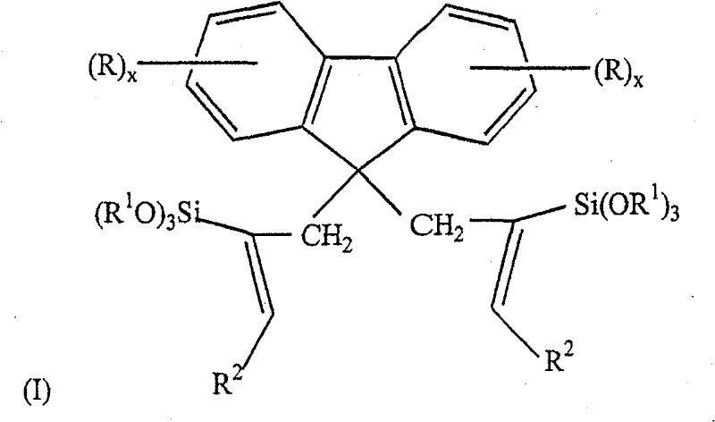
Applications Claiming Priority (2)
| Application Number | Priority Date | Filing Date | Title |
|---|---|---|---|
| US11/013165 | 2004-12-15 | ||
| US11/013,165 US7625596B2 (en) | 2004-12-15 | 2004-12-15 | Adhesion promoter, electroactive layer and electroactive device comprising same, and method |
Publications (2)
| Publication Number | Publication Date |
|---|---|
| CN1796391A CN1796391A (en) | 2006-07-05 |
| CN1796391B true CN1796391B (en) | 2012-02-22 |
Family
ID=35810867
Family Applications (1)
| Application Number | Title | Priority Date | Filing Date |
|---|---|---|---|
| CN2005101134894A Expired - Fee Related CN1796391B (en) | 2004-12-15 | 2005-10-17 | Adhesion promoter, electroactive layer and electroactive device containing same, and method |
Country Status (7)
| Country | Link |
|---|---|
| US (1) | US7625596B2 (en) |
| EP (1) | EP1672718B1 (en) |
| JP (1) | JP5007987B2 (en) |
| KR (1) | KR101134778B1 (en) |
| CN (1) | CN1796391B (en) |
| DE (1) | DE602005025583D1 (en) |
| TW (1) | TWI408193B (en) |
Families Citing this family (29)
| Publication number | Priority date | Publication date | Assignee | Title |
|---|---|---|---|---|
| JP4305425B2 (en) * | 2005-07-20 | 2009-07-29 | セイコーエプソン株式会社 | Electronic devices and electronic equipment |
| US9084546B2 (en) * | 2005-08-31 | 2015-07-21 | The Regents Of The University Of Michigan | Co-electrodeposited hydrogel-conducting polymer electrodes for biomedical applications |
| JP5066805B2 (en) * | 2005-12-12 | 2012-11-07 | 日本電気株式会社 | Electricity storage device |
| US7947148B2 (en) * | 2006-06-01 | 2011-05-24 | The Regents Of The University Of Michigan | Dry adhesion bonding |
| AU2008211760A1 (en) * | 2007-02-02 | 2008-08-07 | G24 Innovations Limited | Photovoltaic cell arrays |
| DE102007021078A1 (en) * | 2007-05-03 | 2008-11-13 | KREUTZER, André | Flat display and method for producing flat displays |
| WO2009025870A1 (en) * | 2007-08-23 | 2009-02-26 | Sri International | Electroluminescent devices employing organic cathodes |
| KR20110008206A (en) | 2008-04-03 | 2011-01-26 | 큐디 비젼, 인크. | Light Emitting Device Including Quantum Dots |
| US9525148B2 (en) | 2008-04-03 | 2016-12-20 | Qd Vision, Inc. | Device including quantum dots |
| ITMI20080927A1 (en) * | 2008-05-20 | 2009-11-21 | Meccaniche Luigi Bander A S P | RELATIVE PHOTOVOLTAIC PANEL PRODUCTION PROCEDURE AND PLANT FOR THE REALIZATION OF SUCH PROCEDURE |
| US7868536B2 (en) * | 2008-10-27 | 2011-01-11 | General Electric Company | Organic light emitting device |
| US9237864B2 (en) | 2009-07-02 | 2016-01-19 | Dexcom, Inc. | Analyte sensors and methods of manufacturing same |
| US20110008525A1 (en) * | 2009-07-10 | 2011-01-13 | General Electric Company | Condensation and curing of materials within a coating system |
| US20120216868A1 (en) * | 2009-10-30 | 2012-08-30 | Takahiro Seike | Manufacturing method of organic photovoltaic cell |
| US9040318B2 (en) * | 2010-04-09 | 2015-05-26 | The Trustees Of Princeton University | Lamination as a modular approach for building organic photosensitive devices |
| KR20130042558A (en) * | 2010-07-16 | 2013-04-26 | 가부시키가이샤 닛폰 쇼쿠바이 | Aqueous electrode binder for secondary battery |
| EP2614513A2 (en) | 2010-09-07 | 2013-07-17 | University College Dublin National University Of Ireland, Dublin | Methods of manufacturing photovoltaic electrodes for dye-sensitized solar cells |
| TW201429708A (en) * | 2012-12-13 | 2014-08-01 | Corning Inc | Glass and methods of making glass articles |
| CN104051651A (en) * | 2013-03-15 | 2014-09-17 | 海洋王照明科技股份有限公司 | Organic electroluminescent device and preparation method thereof |
| CN104051650A (en) * | 2013-03-15 | 2014-09-17 | 海洋王照明科技股份有限公司 | Organic electroluminescent device and preparation method thereof |
| US9362429B2 (en) | 2013-04-30 | 2016-06-07 | Alliance For Sustainable Energy, Llc | Photovoltaic semiconductor materials based on alloys of tin sulfide, and methods of production |
| CN106463678B (en) * | 2014-05-30 | 2020-01-03 | 巴斯夫欧洲公司 | Polymers used as protective layers and other components in electrochemical cells |
| KR102052720B1 (en) | 2016-06-27 | 2019-12-05 | 비아비 솔루션즈 아이엔씨. | High chroma flakes |
| US10928579B2 (en) | 2016-06-27 | 2021-02-23 | Viavi Solutions Inc. | Optical devices |
| US12187900B2 (en) | 2016-06-27 | 2025-01-07 | Viavi Solutions Inc. | High chromaticity pigment flakes and foils |
| CN107033121B (en) * | 2017-05-04 | 2019-05-21 | 华东理工大学 | Four aryl ethylene compound of heterozygosis, polymer and the preparation method and application thereof |
| KR102178216B1 (en) | 2017-09-28 | 2020-11-12 | 주식회사 엘지화학 | A compound useful as an adhesion promoter for polyimide resin and polyimide copolymer prepared using same |
| CN110085833A (en) * | 2019-04-28 | 2019-08-02 | 武汉工程大学 | Coat hollow cubic materials preparation method and its product and application |
| KR102892881B1 (en) | 2020-05-29 | 2025-11-28 | 삼성디스플레이 주식회사 | Hole transporting ink composition, light emitting device, and method for manufacturing the same |
Citations (1)
| Publication number | Priority date | Publication date | Assignee | Title |
|---|---|---|---|---|
| US6596569B1 (en) * | 2002-03-15 | 2003-07-22 | Lucent Technologies Inc. | Thin film transistors |
Family Cites Families (31)
| Publication number | Priority date | Publication date | Assignee | Title |
|---|---|---|---|---|
| US4374760A (en) | 1980-09-12 | 1983-02-22 | Harold Charles | Electro conductive polymer compositions and new materials found useful in their preparation |
| US4898784A (en) * | 1987-12-30 | 1990-02-06 | Shell Oil Company | Tie layer composition and laminated structures containing same |
| JP2656177B2 (en) * | 1991-08-09 | 1997-09-24 | 信越化学工業株式会社 | Distributed EL lamp |
| JP3359073B2 (en) * | 1991-12-24 | 2002-12-24 | 三井化学株式会社 | Organic thin film EL device |
| JPH06313168A (en) * | 1992-05-11 | 1994-11-08 | Idemitsu Kosan Co Ltd | Organic electroluminescent device |
| EP0569827A2 (en) * | 1992-05-11 | 1993-11-18 | Idemitsu Kosan Company Limited | Organic electroluminescence device |
| JPH06124785A (en) * | 1992-10-08 | 1994-05-06 | Idemitsu Kosan Co Ltd | Organic EL element |
| JPH06330034A (en) * | 1993-03-24 | 1994-11-29 | Idemitsu Kosan Co Ltd | Organic electroluminescent device |
| US5503910A (en) * | 1994-03-29 | 1996-04-02 | Idemitsu Kosan Co., Ltd. | Organic electroluminescence device |
| JPH08185973A (en) * | 1994-12-27 | 1996-07-16 | Fuji Xerox Co Ltd | Organic electroluminescent element and its manufacture |
| WO1996033593A1 (en) * | 1995-04-18 | 1996-10-24 | Cambridge Display Technology Limited | Manufacture of organic light emitting devices |
| BR9612111A (en) * | 1995-12-01 | 1999-02-17 | Ciba Geigy Ag | Poli (9'9- spirobisfluorenes), their preparation and use |
| JP4477150B2 (en) * | 1996-01-17 | 2010-06-09 | 三星モバイルディスプレイ株式會社 | Organic thin film EL device |
| US6403236B1 (en) * | 1997-09-04 | 2002-06-11 | Sumitomo Chemical Company, Limited | Polymer light emitting device |
| US5932363A (en) * | 1997-10-02 | 1999-08-03 | Xerox Corporation | Electroluminescent devices |
| GB9722736D0 (en) | 1997-10-29 | 1997-12-24 | Ciba Sc Holding Ag | Adhesive compositions |
| US6248458B1 (en) * | 1997-11-17 | 2001-06-19 | Lg Electronics Inc. | Organic electroluminescent device with improved long-term stability |
| JPH11158648A (en) * | 1997-11-25 | 1999-06-15 | Kitazawa Yakuhin Kk | Surface treatment method |
| JPH11172243A (en) * | 1997-12-10 | 1999-06-29 | Toshiba Corp | Electroluminescent phosphor and method for forming protective film thereof |
| US6525466B1 (en) * | 1999-04-09 | 2003-02-25 | Arizona Board Of Regents On Behalf Of The University Of Arizona | Cathode including a mixture of a metal and an insulator for organic devices and method of making the same |
| JP3940523B2 (en) * | 1999-04-27 | 2007-07-04 | セイコーエプソン株式会社 | Resin composition for inkjet color filter, color filter, and method for producing color filter |
| TWI263636B (en) * | 1999-09-16 | 2006-10-11 | Ciba Sc Holding Ag | Fluorescent maleimides and use thereof |
| JP3819661B2 (en) * | 2000-02-24 | 2006-09-13 | 日東電工株式会社 | Fixing method of pressure-sensitive adhesive sheets and functional films |
| US6358664B1 (en) | 2000-09-15 | 2002-03-19 | 3M Innovative Properties Company | Electronically active primer layers for thermal patterning of materials for electronic devices |
| WO2003013192A1 (en) | 2001-07-27 | 2003-02-13 | The Ohio State University | Methods for fabricating polymer light emitting devices by lamination |
| CN1558921A (en) * | 2001-08-03 | 2004-12-29 | Dsm | Curable composition for display device |
| US6794061B2 (en) * | 2002-01-31 | 2004-09-21 | Eastman Kodak Company | Organic electroluminescent device having an adhesion-promoting layer for use with a magnesium cathode |
| US20040115341A1 (en) | 2002-06-28 | 2004-06-17 | Rantala Juha T. | Adhesion promoter and wetting agent |
| JP4360168B2 (en) * | 2002-10-01 | 2009-11-11 | 東レ株式会社 | Positive photosensitive resin composition |
| US20040232385A1 (en) * | 2003-05-21 | 2004-11-25 | Kram Shari L. | Blend of viscosity modifier and luminescent compound |
| US7101630B2 (en) * | 2003-07-10 | 2006-09-05 | Kawamura Institute Of Chemical Research | Diarylamino group-containing copolymer, organic electroluminescent device, and method of producing hole transport layer for organic electroluminescent device |
-
2004
- 2004-12-15 US US11/013,165 patent/US7625596B2/en not_active Expired - Fee Related
-
2005
- 2005-10-05 TW TW094134845A patent/TWI408193B/en not_active IP Right Cessation
- 2005-10-06 EP EP05256239A patent/EP1672718B1/en not_active Expired - Lifetime
- 2005-10-06 DE DE602005025583T patent/DE602005025583D1/en not_active Expired - Lifetime
- 2005-10-11 JP JP2005296042A patent/JP5007987B2/en not_active Expired - Fee Related
- 2005-10-13 KR KR1020050096595A patent/KR101134778B1/en not_active Expired - Fee Related
- 2005-10-17 CN CN2005101134894A patent/CN1796391B/en not_active Expired - Fee Related
Patent Citations (1)
| Publication number | Priority date | Publication date | Assignee | Title |
|---|---|---|---|---|
| US6596569B1 (en) * | 2002-03-15 | 2003-07-22 | Lucent Technologies Inc. | Thin film transistors |
Also Published As
| Publication number | Publication date |
|---|---|
| KR20060067810A (en) | 2006-06-20 |
| CN1796391A (en) | 2006-07-05 |
| EP1672718A1 (en) | 2006-06-21 |
| US20060127562A1 (en) | 2006-06-15 |
| JP5007987B2 (en) | 2012-08-22 |
| TW200628574A (en) | 2006-08-16 |
| EP1672718B1 (en) | 2010-12-29 |
| DE602005025583D1 (en) | 2011-02-10 |
| JP2006169506A (en) | 2006-06-29 |
| US7625596B2 (en) | 2009-12-01 |
| TWI408193B (en) | 2013-09-11 |
| KR101134778B1 (en) | 2012-04-16 |
Similar Documents
| Publication | Publication Date | Title |
|---|---|---|
| CN1796391B (en) | Adhesion promoter, electroactive layer and electroactive device containing same, and method | |
| US8057918B2 (en) | Organic light-emitting diodes and methods for assembly and enhanced charge injection | |
| US7172822B2 (en) | Network conductor and its production method and use | |
| CN102668158B (en) | Charge transfer film, its preparation method and use its light-emitting component and photo-electric conversion element | |
| EP2549560B1 (en) | Organic electronic device and method of manufacturing the same | |
| JP2000323273A (en) | Electroluminescence element | |
| CN1722339B (en) | Metal compound-metal multilayer electrodes for organic electronic devices | |
| CN102473855A (en) | Polymer Light Emitting Components | |
| CN1883062A (en) | Compound electrodes for electronic devices | |
| KR101451607B1 (en) | Silicone composition and organic light-emitting diode | |
| CN101322259A (en) | Transparent electrodes for organic electronic devices | |
| US20050158579A1 (en) | Organic light-emitting diodes and methods for assembly and enhanced charge injection | |
| WO2017056814A1 (en) | Transparent organic electroluminescence element and method for manufacturing same | |
| US7750175B2 (en) | Organic light-emitting diodes and related hole transport compounds | |
| CN101160673A (en) | Modified electrodes using functional organic materials and electronic devices derived therefrom | |
| JPWO2016084791A1 (en) | Sealing film, functional element, and method for manufacturing sealing film | |
| JP2007529896A (en) | Organic light emitting diode | |
| CN100530745C (en) | Electrophosphorescent arrangement with conducting polymers | |
| JP2015080855A (en) | Sealing film, method for producing the same and functional element sealed with sealing film | |
| JP7112708B2 (en) | Organic EL element | |
| JP3968978B2 (en) | Organic electroluminescence device | |
| JP7487730B2 (en) | Organic electroluminescent element and method for manufacturing organic electroluminescent element | |
| CN119730579A (en) | Flexible transparent conductive electrode with sandwich structure and preparation method thereof | |
| JP2012089261A (en) | Organic electroluminescent element and method of manufacturing the same |
Legal Events
| Date | Code | Title | Description |
|---|---|---|---|
| C06 | Publication | ||
| PB01 | Publication | ||
| C10 | Entry into substantive examination | ||
| SE01 | Entry into force of request for substantive examination | ||
| C14 | Grant of patent or utility model | ||
| GR01 | Patent grant | ||
| CF01 | Termination of patent right due to non-payment of annual fee |
Granted publication date: 20120222 Termination date: 20161017 |
|
| CF01 | Termination of patent right due to non-payment of annual fee |