CN1758495A - Dual-wavelength semiconductor laser light-emitting device and manufacturing method thereof - Google Patents
Dual-wavelength semiconductor laser light-emitting device and manufacturing method thereof Download PDFInfo
- Publication number
- CN1758495A CN1758495A CN 200410084923 CN200410084923A CN1758495A CN 1758495 A CN1758495 A CN 1758495A CN 200410084923 CN200410084923 CN 200410084923 CN 200410084923 A CN200410084923 A CN 200410084923A CN 1758495 A CN1758495 A CN 1758495A
- Authority
- CN
- China
- Prior art keywords
- coating layer
- laser light
- layer
- current injection
- emitting element
- Prior art date
- Legal status (The legal status is an assumption and is not a legal conclusion. Google has not performed a legal analysis and makes no representation as to the accuracy of the status listed.)
- Granted
Links
Images


Landscapes
- Semiconductor Lasers (AREA)
Abstract
Description
技术领域technical field
本发明涉及一种双波长半导体激光发光装置及制造方法,特别是涉及在一基板上两颗不同的激光发光元件,此两颗不同的激光发光元件可分别振荡不同波长的激光。The invention relates to a dual-wavelength semiconductor laser light-emitting device and a manufacturing method, in particular to two different laser light-emitting elements on a substrate, and the two different laser light-emitting elements can respectively oscillate laser light of different wavelengths.
背景技术Background technique
在一基板上要形成具有双波长激光发光元件的半导体激光发光装置,现有的作法大都是在一基板上形成两颗各自独立激光发光元件,这两颗发光元件分别有独立的下包覆层、有源层及上包覆层。现有技术例如美国专利公告号6,468,820及美国专利公开号2003/0197204 A1中对此相关技术有详细介绍,在此仅提供如图1的简要图示以作为现有技术的说明。To form a semiconductor laser light-emitting device with a dual-wavelength laser light-emitting element on a substrate, most of the existing methods are to form two independent laser light-emitting elements on a substrate, and the two light-emitting elements have independent lower cladding layers respectively. , an active layer and an upper cladding layer. Prior art such as US Patent No. 6,468,820 and US Patent Publication No. 2003/0197204 A1 have introduced this related technology in detail, and here only a brief diagram as shown in FIG. 1 is provided as an explanation of the prior art.
如图1所示,在基板30上有一第一激光发光元件区域以I代表、及第二激光发光元件区域以II代表。第一激光发光元件10的第一下包覆层111及第二激光发光元件20的第二下包覆层211各自独立地形成在基板30上。这种结构的制造方法包括多次蚀刻步骤。例如,在沉积第一复合层11之后,必需藉由蚀刻以去除不在区域I的第一复合层11,如此第二激光发光元件20才能形成在基板30上。而且,因为沉积第二复合层21在基板30上时也会同时沉积在第一复合层11的表面上,所以也要藉由蚀刻以去除第一激光区上的第二复合层21。再者,第一激光元件10及第二激光元件10的隔离阱60也是要透过蚀刻工艺加以定义。As shown in FIG. 1 , on the
由于一般蚀刻工艺的实施先后牵涉到掩模的形成及去除等繁复步骤,蚀刻次数太多将增加制造成本,较不具经济效益。因此设计一套更简易的制造方法,减少工艺步骤来制造一种具有双波长激光发光元件的新颖性半导体激光装置是有其必要的。Since the implementation of the general etching process involves complex steps such as mask formation and removal, too many times of etching will increase the manufacturing cost, which is less economical. Therefore, it is necessary to design a simpler manufacturing method and reduce process steps to manufacture a novel semiconductor laser device with a dual-wavelength laser light-emitting element.
发明内容Contents of the invention
本发明的任务是提供一种双波长半导体激光发光装置及其制造方法,以设计一套更简易的制造方法,减少工艺步骤来制造一种具有双波长激光发光元件的新颖性半导体激光装置。The task of the present invention is to provide a dual-wavelength semiconductor laser light-emitting device and its manufacturing method, so as to design a simpler manufacturing method and reduce process steps to manufacture a novel semiconductor laser device with a dual-wavelength laser light-emitting element.
为此,本发明一方面提供一种双波长半导体激光发光装置,包括:To this end, the present invention provides a dual-wavelength semiconductor laser light-emitting device on the one hand, comprising:
一基板;a substrate;
一第一激光发光元件,形成在该基板上,该第一激光发光元件具有一第一下包覆层、一第一有源层及一第一上包覆层;以及A first laser light-emitting element, formed on the substrate, the first laser light-emitting element has a first lower cladding layer, a first active layer, and a first upper cladding layer; and
一第二激光发光元件,形成在该基板上,该第二激光发光元件具有一第二下包覆层、一第二有源层及一第二上包覆层;A second laser light-emitting element, formed on the substrate, the second laser light-emitting element has a second lower cladding layer, a second active layer, and a second upper cladding layer;
其中,该第二有源层堆栈在该第一上包覆层的上方,使该第一上包覆层作为该第二激光发光元件的第二下包覆层。Wherein, the second active layer is stacked on the first upper cladding layer, so that the first upper cladding layer serves as the second lower cladding layer of the second laser light emitting element.
本发明另一方面提供一种用来制造半导体激光发光元件发光装置的方法,该方法包括下列步骤:Another aspect of the present invention provides a method for manufacturing a semiconductor laser light-emitting element light-emitting device, the method comprising the following steps:
(a)提供一基板,该基板具有一第一激光发光元件的一第一下包覆层、一第一有源层及一第一上包覆层;(a) providing a substrate having a first lower cladding layer, a first active layer, and a first upper cladding layer of a first laser light-emitting element;
(b)以该第一上包覆层作为一第二激光发光元件的一第二下包覆层,堆栈该第二激光发光元件的一第二有源层及一第二上包覆层于该第一上包覆层的上方。(b) using the first upper cladding layer as a second lower cladding layer of a second laser light emitting element, stacking a second active layer and a second upper cladding layer of the second laser light emitting element on above the first upper cladding layer.
根据本发明的一种双波长半导体激光发光装置及制造方法,此装置包括形成在一基板上的一第一激光发光元件及一第二激光发光元件。制造方法将第二激光发光元件的一有源层堆栈在第一激光发光元件的一上包覆层的上方,使第一激光发光元件与该第二激光发光元件具有一共享电极,并可分别振荡不同波长的激光。According to a dual-wavelength semiconductor laser light-emitting device and manufacturing method of the present invention, the device includes a first laser light-emitting element and a second laser light-emitting element formed on a substrate. The manufacturing method stacks an active layer of the second laser light-emitting element on top of an upper cladding layer of the first laser light-emitting element, so that the first laser light-emitting element and the second laser light-emitting element have a common electrode, and can be respectively Lasers of different wavelengths are oscillated.
附图说明Description of drawings
图1:现有的半导体激光发光装置剖面图;Figure 1: A cross-sectional view of an existing semiconductor laser light emitting device;
图2a-2n:说明本发明的一实施例的工艺步骤的剖面图;Figures 2a-2n: cross-sectional views illustrating process steps of an embodiment of the present invention;
图3a-3l:说明本发明的另一实施例的工艺步骤的剖面图。Figures 3a-3l: Cross-sectional views illustrating process steps of another embodiment of the present invention.
简单符号说明simple notation
第一激光发光元件10The first laser
第一复合层11first
第一n型下包覆层111The first n-type
第一有源层112first
第一p型上包覆层113The first p-type
第一脊状电流注入区113rThe first ridge
第一非脊状电流注入区113nThe first non-ridge
第一p型欧姆接触层17The first p-type
第二激光发光元件20Second laser
第二复合层21
第二下包覆层211Second
第二有源层212second
第二n型上包覆层213The second n-type
第二脊状电流注入区(current injection region in a ridge form)213rThe second ridge current injection region (current injection region in a ridge form) 213r
第二非脊状电流注入区213nThe second non-ridge
沟槽23、25Groove 23, 25
第二n型欧姆接触层27The second n-type
n型基板30n-
钝化层40
掩模51、52、53、54、55、56、57、58
隔离阱60isolation well 60
具体实施方式Detailed ways
在此提供两个实施例以详加说明本发明的半导体激光发光装置及其制造方法,其中图2a到图2n用来说明实施例1,图3a到图3l则用来说明实施例2。Two embodiments are provided here to illustrate the semiconductor laser light-emitting device and its manufacturing method of the present invention in detail, wherein FIG. 2a to FIG. 2n are used to illustrate
参考实施例1的图2a,提供由GaAs所组成的一n型基板30,在n型基板30上预先区分第一激光发光元件区域I、及第二激光发光元件区域II。n型基板30表面上具有第一复合层11。第一复合层11包括由AlGaAs所组成的第一n型下包覆层111、可振荡一特定波长的多重量子阱结构(multiplequantum well structure)的第一有源层112、及由AlGaAs所组成的第一p型上包覆层113,依次地堆栈在n型基板30上方。第一p型上包覆层113藉蚀刻形成一第一脊状电流注入区113r及一第一非脊状电流注入区113n,其中第一脊状电流注入区113r位在区域I中。Referring to FIG. 2 a of
参考图2b,利用一般微影技术在第一脊状电流注入区113r的上方形成掩模51。接着,参考图2c,采用现有的有机金属蒸气相外延成长(Metal-Organic Vapor Phase Epitaxial Growth,MOVPE)技术,选择性地(selective)对掩模51,在第一非脊状电流注入区113n的上方依次堆栈第二有源层212、及由AlGaAs所组成的第二n型上包覆层213。第二有源层212具有可振荡一特定波长的多重量子阱结构。第二激光振荡波长与第一激光振荡波长可不相同,例如分别为650nm及780nm。如图2c所示,第二有源层212及第二n型上包覆层213合称为一第二复合层21。Referring to FIG. 2b, a
接着,参考图2d-2e。在第二复合层21表面上形成有图案的掩模52。然后藉由蚀刻方式在区域II的第二n型上包覆层213表面上定义一沟槽23及一沟槽25。控制蚀刻速度使蚀刻不会穿透第二n型上包覆层213而侵蚀到第二有源层212,意即沟槽23及沟槽25的底部仍为第二n型上包覆层213,如图2e所示。将掩模52去除之后,第二n型上包覆层213在沟槽23及沟槽25之间的区域即形成第二脊状电流注入区213r。在第二n型上包覆层213表面上,排除第二脊状电流注入区213r、沟槽23及沟槽25,其余的区域即为第二非脊状电流注入区213n,如图2f所示。Next, reference is made to Figures 2d-2e. A patterned
参考图2g,在第二脊状电流注入区上方形成一掩模53。然后采用现有沉积工艺,例如CVD或PVD,选择性地(selective)对掩模51及掩模53,在第二非脊状电流注入区213r的上方表面共形地形成一钝化层40。钝化层40是用来隔离第二n型非脊状电流注入区213n与之后将要形成的第二n型欧姆接触层。钝化层40的材料可为一般含硅、氧或氮的绝缘材料所组成。Referring to FIG. 2g, a mask 53 is formed over the second ridge current injection region. Then, a
然后,进一步说明第二激光发光元件的第二n型欧姆接触层的制作。如图2h所示,藉由选择性蚀刻去除掩模51及掩模53。接着,如图2i所示形成一掩模54覆盖区域I的钝化层40的上表面及第一脊状电流注入区113r的上表面。接着,采用PVD技术,选择性地(selective)对掩模54,沉积一第二n型欧姆接触层27覆盖区域II的钝化层40的上表面及第二脊状电流注入区213r的上表面,如图2j所示。第二n型欧姆接触层27的材料由导电金属所组成。然后,藉由选择性蚀刻将掩模54去除,如图2k所示。Next, the fabrication of the second n-type ohmic contact layer of the second laser light-emitting element will be further described. As shown in FIG. 2h,
图2l-2n进一步说明第一激光元件的第一p型欧姆接触层的制作。第一p型欧姆接触层即为第一激光发光元件10及第二激光发光元件20的共享电极,操作方式在后面将有详细说明。如图2l所示,形成一掩模55覆盖第二n型欧姆接触层27及钝化层40位于第一p型脊状电流注入区113r及第二n型欧姆接触层27之间的区域。接着,藉由PVD技术,选择性地(selective)对掩模55,沉积一第一p型欧姆接触层17覆盖住没有被掩模55覆盖的表面。第一p型欧姆接触层17的材料可由导电金属所组成。然后,如图2n所示,藉由选择性蚀刻将掩模55去除。应要注意的是,掩模55去除之后,第一p型欧姆接触层17与第二n型欧姆接触层27之间将形成一隔离阱60。2l-2n further illustrate the fabrication of the first p-type ohmic contact layer of the first laser element. The first p-type ohmic contact layer is the common electrode of the first laser
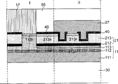
图2n即显示依据本发明所制作的双波长半导体激光发光装置。此装置包括形成在基板30上的第一激光发光元件10及第二激光发光元件20。其中第二激光发光元件20的第二有源层212直接堆栈在第一激光发光元件10的第一上包覆层113的上方,因此第一激光发光元件10与该第二激光发光元件20即具有一共享阳极(即第一p型欧姆接触层17)。操作此双波长半导体激光发光装置时,可将此共享阳极接地,第一激光发光元件的信号线1与第一n型下包覆层111电连接,第二激光发光元件的信号线2则与第二n型欧姆接触层27电连接。为了使这两颗激光发光元件在不同的时间运作,当对信号线1施加正偏压时也要同时对信号线2施加负偏压,或对信号线1施加负偏压时要同时对信号线2施加正偏压,如此即可使第一激光发光元件10与第二激光发光元件20在不同时间分别振荡其特定波长的激光。要注意的是,本发明接地端的位置与图1所示的现有技术并不相同。现有的接地端一般是设置在基板30上,然本发明的接地端则是设置在第一激光发光元件10的第一欧姆接触层17上。FIG. 2n shows a dual-wavelength semiconductor laser light-emitting device manufactured according to the present invention. The device includes a first laser
本领域技术人员应可了解,依照上述的相同方式只要轻易变化材料也可以制造出一共享阴极的结构。Those skilled in the art should understand that a shared cathode structure can also be produced by simply changing the material in the same manner as above.
接下来说明实施例2。在实施例2的图3a-3l中,与实施例1相同的元件采用相同的元件符号。另外,显示在图3a-3c的实施例2的工艺步骤与实施例1的图2a-2c相同,故在此不予赘述。直接参考图3d,利用现有的微影工艺技术在区域II第二复合层21表面上形成一掩模56。然后,选择性蚀刻没有被掩模51及掩模56覆盖的第二n型上包覆层213,并且控制蚀刻速度使蚀刻不会穿透第二n型上包覆层213而侵蚀到第二有源层212。因此,第二n型上包覆层213被掩模56所覆盖区域即形成第二脊状电流注入区213r,而且排除第二脊状电流注入区213r的第二n型上包覆层213的剩余区域即为第二非脊状电流注入区213n。Next, Example 2 will be described. In Figures 3a-3l of
参考图3e,采用现有沉积工艺,例如CVD或PVD,选择性地(selective)对掩模51及掩模56,在第二非脊状电流注入区213n的上方沉积一钝化层40。钝化层40是用来隔离第二n型非脊状电流注入区213n与之后将要形成的第二欧姆接触层。钝化层40的材料可为一般含硅、氧或氮的绝缘材料所组成。Referring to FIG. 3 e , a
然后,进一步说明第二激光发光元件的第二n型欧姆接触层的制作。如图3f所示,藉由选择性蚀刻去除掩模51及掩模56。接着,如图3g所示形成一掩模57覆盖区域I的钝化层40的上表面及第一脊状电流注入区113r的上表面。接着,如图3h所示,采用PVD技术,选择性地(selective)对掩模57,沉积一第二n型欧姆接触层27覆盖区域II的钝化层40的上表面及第二脊状电流注入区213r的上表面。第二n型欧姆接触层27的材料可由导电金属所组成。然后,藉由选择性蚀刻将掩模57去除,如图3i所示。Next, the fabrication of the second n-type ohmic contact layer of the second laser light-emitting element will be further described. As shown in FIG. 3f,
图3j-3l进一步说明第一激光元件的第一p型欧姆接触层的制作。如图3j所示,形成一掩模58覆盖第二n型欧姆接触层27及位于第一脊状电流注入区113r及第二n型欧姆接触层27之间的钝化层40。接着,藉由PVD技术,选择性地(selective)对掩模58,沉积一第一p型欧姆接触层17覆盖住没有被掩模58覆盖的表面,如图3k所示。第一p型欧姆接触层17的材料可由导电金属所组成。然后,藉由选择性蚀刻将掩模58去除,如图3l所示。应要注意的是,掩模58去除之后,第一p型欧姆接触层17与第二n型欧姆接触层27之间将形成一隔离阱60。3j-3l further illustrate the fabrication of the first p-type ohmic contact layer of the first laser element. As shown in FIG. 3 j , a
实施例2所制作的半导体激光发光装置,如图3l所示,第一激光发光元件10与第二激光发光元件20也是在n型基板30上形成共享阳极的结构。此结构的操作方式与实施例1相同。同样地,本领域技术人员应可了解,依照本案相同的方式只要轻易变化材料也可以制造出共享阴极的结构。In the semiconductor laser light-emitting device produced in Example 2, as shown in FIG. 31 , the first laser light-emitting
以上优选实施例的详述,希望能更加清楚描述本发明的特征与精神,而上述所揭露的优选实施例并非对本发明的范畴的限制。相反地,上述的说明以及各种改变及均等性的安排皆为本发明所欲受到保护的范畴。因此,本发明权利要求的范畴应此根据上述的说明作最宽广的解释,并涵盖所有可能均等的改变以及具均等性的安排。The above detailed description of the preferred embodiments hopes to describe the features and spirit of the present invention more clearly, but the preferred embodiments disclosed above do not limit the scope of the present invention. On the contrary, the above description and various changes and equivalent arrangements are all within the scope of protection of the present invention. Therefore, the scope of the claims of the present invention should be interpreted in the broadest way based on the above description, and cover all possible equivalent changes and equivalent arrangements.
Claims (10)
Priority Applications (1)
| Application Number | Priority Date | Filing Date | Title |
|---|---|---|---|
| CNB2004100849236A CN100377457C (en) | 2004-10-10 | 2004-10-10 | Dual wavelength semiconductor laser light emitting device and method of manufacturing the same |
Applications Claiming Priority (1)
| Application Number | Priority Date | Filing Date | Title |
|---|---|---|---|
| CNB2004100849236A CN100377457C (en) | 2004-10-10 | 2004-10-10 | Dual wavelength semiconductor laser light emitting device and method of manufacturing the same |
Publications (2)
| Publication Number | Publication Date |
|---|---|
| CN1758495A true CN1758495A (en) | 2006-04-12 |
| CN100377457C CN100377457C (en) | 2008-03-26 |
Family
ID=36703745
Family Applications (1)
| Application Number | Title | Priority Date | Filing Date |
|---|---|---|---|
| CNB2004100849236A Expired - Lifetime CN100377457C (en) | 2004-10-10 | 2004-10-10 | Dual wavelength semiconductor laser light emitting device and method of manufacturing the same |
Country Status (1)
| Country | Link |
|---|---|
| CN (1) | CN100377457C (en) |
Family Cites Families (3)
| Publication number | Priority date | Publication date | Assignee | Title |
|---|---|---|---|---|
| US5071786A (en) * | 1990-03-08 | 1991-12-10 | Xerox Corporation | Method of making multiple wavelength p-n junction semiconductor laser with separated waveguides |
| JPH11112091A (en) * | 1997-09-30 | 1999-04-23 | Victor Co Of Japan Ltd | Semiconductor laser device |
| US6546035B2 (en) * | 2000-02-29 | 2003-04-08 | Matsushita Electric Industrial Co., Ltd. | Semiconductor laser diode array and method of fabricating the same |
-
2004
- 2004-10-10 CN CNB2004100849236A patent/CN100377457C/en not_active Expired - Lifetime
Also Published As
| Publication number | Publication date |
|---|---|
| CN100377457C (en) | 2008-03-26 |
Similar Documents
| Publication | Publication Date | Title |
|---|---|---|
| US20250089429A1 (en) | Led arrays with dbr | |
| CN1729581A (en) | Method of forming semiconductor mesa structure including self-aligned contact layer and related device | |
| US7406111B2 (en) | Semiconductor laser diode and method for manufacturing the same | |
| TW200828707A (en) | Multiwavelength semiconductor laser array and method of manufacturing the same | |
| JP2007227938A (en) | Nitride-based semiconductor light-emitting device and manufacturing method thereof | |
| CN1360376A (en) | Luminous semiconductor device with improved electroptical characteristic and mfg. method therefor | |
| US20230048093A1 (en) | Micro-led and method of manufacture | |
| KR20100073757A (en) | Light emitting device using micro-rod and method of manufacturing the light emitting device | |
| US8501510B2 (en) | Optoelectronic component with three-dimension quantum well structure and method for producing the same | |
| US20230378237A1 (en) | Led device and method of manufacture | |
| KR20060131652A (en) | Single EL Growth P-N Lateral Junction Nitride Semiconductor Laser Manufacturing Method and Semiconductor Laser Structure | |
| CN1744396A (en) | Method of fabricating laser diode | |
| CN112151650A (en) | Micro light-emitting diode array and preparation method thereof | |
| KR101845611B1 (en) | High Efficiency Light Emitting Diode Having Optical Functionalized Electrodes | |
| JP2022543821A (en) | LED arrays and methods of forming LED arrays | |
| CN1758495A (en) | Dual-wavelength semiconductor laser light-emitting device and manufacturing method thereof | |
| JP2008135441A (en) | Two-dimensional photonic crystal surface emitting laser and manufacturing method thereof | |
| CN1283030C (en) | Array type single transverse mode surface emitting laser device and manufacturing method thereof | |
| US20230317877A1 (en) | Semiconductor light-emitting device and manufacturing method thereof | |
| JP4497606B2 (en) | Semiconductor laser device | |
| TW202123487A (en) | Light emitting diode and method of forming a light emitting diode | |
| US20230109404A1 (en) | Semiconductor Light-Emitting Device And Preparation Method Thereof | |
| US7184456B2 (en) | Dual wavelength semiconductor laser emitting apparatus and manufacturing method thereof | |
| JP2024159042A (en) | Semiconductor light emitting device | |
| KR20230059314A (en) | LED structure, ink for ink-jet and light source comprising the same |
Legal Events
| Date | Code | Title | Description |
|---|---|---|---|
| C06 | Publication | ||
| PB01 | Publication | ||
| C41 | Transfer of patent application or patent right or utility model | ||
| TA01 | Transfer of patent application right |
Effective date of registration: 20060310 Address after: Hsinchu city of Taiwan Province Applicant after: EPISTAR Corp. Address before: Hsinchu Science Industrial Park, Taiwan Applicant before: UNITED EPITAXY CO.,LTD. |
|
| C10 | Entry into substantive examination | ||
| SE01 | Entry into force of request for substantive examination | ||
| C14 | Grant of patent or utility model | ||
| GR01 | Patent grant | ||
| CX01 | Expiry of patent term |
Granted publication date: 20080326 |
|
| CX01 | Expiry of patent term |