CN1501165A - Device manufacturing method and device produced therefrom - Google Patents
Device manufacturing method and device produced therefrom Download PDFInfo
- Publication number
- CN1501165A CN1501165A CNA200310116131A CN200310116131A CN1501165A CN 1501165 A CN1501165 A CN 1501165A CN A200310116131 A CNA200310116131 A CN A200310116131A CN 200310116131 A CN200310116131 A CN 200310116131A CN 1501165 A CN1501165 A CN 1501165A
- Authority
- CN
- China
- Prior art keywords
- substrate
- layer
- alignment
- protective layer
- alignment marks
- Prior art date
- Legal status (The legal status is an assumption and is not a legal conclusion. Google has not performed a legal analysis and makes no representation as to the accuracy of the status listed.)
- Pending
Links
Images


Classifications
-
- G—PHYSICS
- G03—PHOTOGRAPHY; CINEMATOGRAPHY; ANALOGOUS TECHNIQUES USING WAVES OTHER THAN OPTICAL WAVES; ELECTROGRAPHY; HOLOGRAPHY
- G03F—PHOTOMECHANICAL PRODUCTION OF TEXTURED OR PATTERNED SURFACES, e.g. FOR PRINTING, FOR PROCESSING OF SEMICONDUCTOR DEVICES; MATERIALS THEREFOR; ORIGINALS THEREFOR; APPARATUS SPECIALLY ADAPTED THEREFOR
- G03F9/00—Registration or positioning of originals, masks, frames, photographic sheets or textured or patterned surfaces, e.g. automatically
- G03F9/70—Registration or positioning of originals, masks, frames, photographic sheets or textured or patterned surfaces, e.g. automatically for microlithography
- G03F9/7003—Alignment type or strategy, e.g. leveling, global alignment
-
- H10P76/00—
Landscapes
- Physics & Mathematics (AREA)
- General Physics & Mathematics (AREA)
- Exposure And Positioning Against Photoresist Photosensitive Materials (AREA)
- Exposure Of Semiconductors, Excluding Electron Or Ion Beam Exposure (AREA)
Abstract
一种器件制造方法,包括步骤:提供具有第一和第二表面的第一衬底;使所述衬底的所述第一表面形成具有至少一个倒转对准标记的图案;在所述对准标记上提供保护层;将所述第一衬底的所述第一表面粘合到第二衬底上;将所述第一衬底局部地蚀刻到所述保护层,以形成围绕在所述或各所述倒转对准标记周围的沟槽;以及采用具有正-反面对准系统的光刻投影装置来在所述第二表面上形成至少一个图案层,同时使所述衬底与显露于所述或各所述沟槽中的对准标记对齐。
A method of manufacturing a device, comprising the steps of: providing a first substrate having a first surface and a second surface; forming a pattern having at least one inverted alignment mark on the first surface of the substrate; providing a protective layer on the mark; bonding the first surface of the first substrate to a second substrate; partially etching the first substrate into the protective layer to form a or grooves around each of the inverted alignment marks; and using a photolithographic projection device with a front-back alignment system to form at least one pattern layer on the second surface, while making the substrate and the exposed The alignment marks in the or each said trench are aligned.
Description
技术领域technical field
本发明涉及采用光刻投影装置的器件制造方法,该光刻投影装置包括:The present invention relates to a device manufacturing method using a lithography projection device, the lithography projection device comprising:
-用于提供辐射投影光束的辐射系统;- a radiation system for providing a radiation projection beam;
-用于按照所需的图案来使投影光束形成图案的图案形成装置;- patterning means for patterning the projection beam according to a desired pattern;
-用于固定衬底的衬底台;和- a substrate table for holding the substrate; and
-用于将形成图案的光束投影到衬底第一侧上的目标部分上的投影系统。- A projection system for projecting the patterned light beam onto a target portion on the first side of the substrate.
背景技术Background technique
光刻装置是一种将所需的图案施加到衬底的目标部分上的机器。光刻装置例如可用于集成电路(IC)的制造中。在这种情况下,图案形成装置如掩模可用于产生与IC的单个层相对应的电路图案,而且此图案可成像于具有一层辐射敏感材料(抗蚀剂)的衬底(如硅晶片)上的目标部分(例如包括一个或多个管心)上。通常来说,单个衬底包含被连续曝光的相邻目标部分的网络。已知的光刻装置包括所谓的分档器,其中通过将整个图案一次性地曝光到目标部分上来照射各目标部分;还包括所谓的扫描器,其中通过沿给定方向(“扫描”方向)经投影光束扫描图案并以平行于或反向平行于此方向的方向同步地扫描衬底来照射各目标部分。A lithographic apparatus is a machine that applies a desired pattern to a target portion of a substrate. A lithographic apparatus may be used, for example, in the manufacture of integrated circuits (ICs). In this case, a patterning device such as a mask can be used to create a circuit pattern corresponding to the individual layers of the IC, and this pattern can be imaged on a substrate (such as a silicon wafer) with a layer of radiation-sensitive material (resist). ) on the target portion (eg, including one or more cores). Typically, a single substrate contains a network of adjacent target portions that are sequentially exposed. Known lithographic apparatuses include so-called steppers, in which each target portion is irradiated by exposing the entire pattern onto the target portion at once; The projected beam scans the pattern and scans the substrate synchronously in a direction parallel or anti-parallel to this direction to illuminate target portions.
对准是将掩模上特定点的图像定位在待曝光晶片的特定点上的工艺。通常在衬底和掩模上均设置一个或多个对准标记,例如小的图案。器件可包括许多层,其通过用中间处理步骤来连续地曝光而构成。在各次曝光之前使衬底和掩模上的标记对准,从而降低新的曝光和前次曝光之间的任何位置误差,这种误差称为重叠误差。Alignment is the process of positioning the image of specific points on the mask at specific points on the wafer to be exposed. Typically one or more alignment marks, such as small patterns, are provided on both the substrate and the mask. A device may comprise many layers constructed by successive exposures with intermediate processing steps. Aligning the marks on the substrate and mask prior to each exposure reduces any positional error between the new exposure and the previous exposure, known as overlay error.
对于一些器件如微型电-机械系统(MEMS)和微型光-电-机械系统(MOEMS)来说,希望能够采用光刻工艺来在衬底的两侧上形成一定的结构,在许多情况下,衬底的相对侧上的结构需要相互对准。这意味着光刻装置必须使被投影到衬底正面上的图案与背面上的对准标记对齐。这可用另外的硬件、例如可将背面标记的图像投影到衬底正面上的光学元件来完成,或者使用透明的衬底。对硅衬底来说可使用红外线辐射,但其精度有限且可能会不合需要地加热晶片。For some devices such as micro-electro-mechanical systems (MEMS) and micro-opto-electric-mechanical systems (MOEMS), it is hoped that photolithography can be used to form certain structures on both sides of the substrate. In many cases, The structures on opposite sides of the substrate need to be aligned with each other. This means that the lithographic apparatus must align the pattern projected onto the front side of the substrate with the alignment marks on the back side. This can be done with additional hardware, such as optics that can project the image of the backside marking onto the front side of the substrate, or using a transparent substrate. Infrared radiation can be used for silicon substrates, but has limited accuracy and may undesirably heat the wafer.
发明内容Contents of the invention
本发明的一个目的是提供一种器件制造方法,其可在衬底的一侧上印刷与另一侧上的标记对齐的结构,该方法不需要另外的硬件,并且具有提高的精度。It is an object of the present invention to provide a method of device fabrication which can print structures on one side of a substrate aligned with markings on the other side, which method does not require additional hardware and has increased precision.
这些和其它的目的可由根据本发明的器件制造方法来实现,其包括:These and other objects can be achieved by a device manufacturing method according to the present invention, which includes:
提供具有第一和第二表面的第一衬底;providing a first substrate having first and second surfaces;
使所述衬底的所述第一表面形成具有至少一个倒转对准标记的图案;patterning the first surface of the substrate with at least one inverted alignment mark;
在所述对准标记上提供保护层;providing a protective layer over the alignment marks;
将所述第一衬底的所述第一表面粘合到第二衬底上;bonding the first surface of the first substrate to a second substrate;
将所述第一衬底局部地蚀刻到所述保护层,以形成围绕在所述或各所述倒转对准标记周围的沟槽;和partially etching the first substrate into the protective layer to form a trench surrounding the or each inverted alignment mark; and
采用具有正-反面对准系统的光刻投影装置来在所述第二表面上形成至少一个图案层,同时使所述衬底与显露于所述或各所述沟槽中的对准标记对齐。using a lithographic projection apparatus having a front-back alignment system to form at least one patterned layer on said second surface while aligning said substrate with alignment marks exposed in said or each said trench .
形成于第一表面内的倒转对准标记通过蚀刻显露出,作为正常定向的对准标记,光刻投影装置可以容易地对准此标记。因此,与印刷在正面上的标记直接对齐的图案就可印刷到衬底的背面上。The inverted alignment mark formed in the first surface is revealed by etching as a normally oriented alignment mark to which a lithographic projection apparatus can be easily aligned. Thus, patterns can be printed onto the backside of the substrate in direct alignment with indicia printed on the front side.
与标记的形状相一致的保护层最好由例如SiO2的材料形成,其选择成可抵抗用于形成沟槽的蚀刻,因而形成了蚀刻终止层。在保护层上可形成反射层如Al层(在粘合前),以便提高标记在显露于沟槽中时的可见性。The protective layer conforming to the shape of the indicia is preferably formed from a material such as SiO2 selected to resist the etch used to form the trench, thus forming an etch stop layer. A reflective layer such as an Al layer can be formed on the protective layer (before bonding) to improve the visibility of the markings when they are exposed in the grooves.
蚀刻步骤可如下所述地于局部处进行:在第二表面上形成蚀刻阻挡层,例如氧化物层;在蚀刻阻挡层上提供辐射敏感的抗蚀剂层;使所述抗蚀剂形成图案并对其进行显影,以形成位于所述标记上方的开口;以及除去所述开口内的所述蚀刻阻挡层。为了使抗蚀剂形成图案以形成开口,只需粗略地定位标记,这可通过从衬底的第二侧使用红外标记传感器来足够高精度地完成。The etching step may be performed locally as follows: forming an etch barrier layer, such as an oxide layer, on the second surface; providing a radiation sensitive resist layer on the etch barrier layer; patterning the resist and developing it to form an opening over the mark; and removing the etch stop layer within the opening. In order to pattern the resist to form the openings, the marks need only be roughly positioned, which can be done with sufficient accuracy using an infrared mark sensor from the second side of the substrate.
在将衬底粘合到第二(载体)衬底上之前,可采用已知的技术在第一表面中和/或在其上形成器件。保护层和可选择的反射层可形成为器件层的一部分,在必要时可局部地除去任何中间层而不是专门地形成一些中间层。Known techniques may be used to form devices in and/or on the first surface prior to bonding the substrate to the second (carrier) substrate. The protective layer and optional reflective layer may be formed as part of the device layers, and any intermediate layers may be partially removed if necessary rather than some intermediate layers being exclusively formed.
用于对准第一表面上或其中的结构的正常对准标记可在与用于对准形成于第二表面上的结构的倒转对准标记相同的步骤中印刷。这样就可以保证正常标记和倒转标记之间的位置关系,并因而保证第一和第二表面上的结构之间的位置关系。Normal alignment marks for aligning structures on or in the first surface may be printed in the same step as inverted alignment marks for aligning structures formed on the second surface. This ensures the positional relationship between the normal mark and the inverted mark, and thus between the structures on the first and second surfaces.
在粘合后,例如通过磨削来使第一衬底的厚度减小。After bonding, the thickness of the first substrate is reduced, for example by grinding.
虽然在本文中将具体地参考IC制造中的光刻装置的使用,然而应当理解,这里所介绍的光刻装置还具有其它应用,例如集成光学系统、用于磁畴存储器的引导和检测图案、液晶显示器(LCD)、薄膜磁头等的制造。本领域的技术人员可以理解,在这种替代性应用的上下文中,用语“晶片”或“管心”在这里的任何使用分别被视为与更通用的用语“衬底”或“目标区域”具有相同的含义。这里所指的衬底可在曝光前或曝光后例如在轨道(一种通常在衬底上施加抗蚀层并对暴露出来的抗蚀层进行显影的工具)或度量或检查工具中进行加工。在适当之处,这里的公开内容可应用于这些和其它衬底加工工具中。另外,衬底可被不止一次地加工,例如以形成多层IC,因此,这里所用的用语“衬底”也可指已经包含有多层已加工的层的衬底。Although specific reference will be made herein to the use of lithographic apparatus in IC fabrication, it should be understood that the lithographic apparatus described here also has other applications, such as integrated optical systems, guiding and detection patterns for magnetic domain memories, Manufacture of liquid crystal displays (LCDs), thin-film magnetic heads, etc. Those skilled in the art will appreciate that any use of the terms "wafer" or "die" herein in the context of this alternative application is to be considered incompatible with the more general terms "substrate" or "target area", respectively. have the same meaning. The substrate referred to herein may be processed, for example, in a track (a tool that typically applies a resist layer to a substrate and develops the exposed resist layer) or a metrology or inspection tool, either before or after exposure. Where appropriate, the disclosure herein may be applied to these and other substrate processing tools. In addition, a substrate may be processed more than once, eg, to form a multilayer IC, and thus, the term "substrate" as used herein may also refer to a substrate that already contains multiple processed layers.
这里所用的用语“辐射”和“光束”用于包括所有类型的电磁辐射,包括紫外线(UV)辐射(例如波长为365,248,193,157或126毫微米)和远紫外线(EUV)辐射(例如具有5-20毫微米范围内的波长),以及粒子束辐射,例如离子束或电子束辐射。The terms "radiation" and "beam" as used herein are intended to include all types of electromagnetic radiation, including ultraviolet (UV) radiation (e.g., at wavelengths of 365, 248, 193, 157 or 126 For example with wavelengths in the range of 5-20 nanometers), and particle beam radiation, such as ion beam or electron beam radiation.
这里所用的用语“图案形成装置”应被广义地解释为可用于使投影光束的横截面具有一定的图案以便在衬底的目标部分中形成图案的装置。应当注意的是,施加于投影光束中的图案可以不精确地对应于衬底目标部分中的所需图案。一般来说,施加于投影光束中的图案将对应于器件中的将形成于目标部分内的特定功能层,例如集成电路。The term "patterning device" as used herein should be interpreted broadly as a device that can be used to pattern the cross-section of a projection beam to form a pattern in a target portion of a substrate. It should be noted that the pattern imparted in the projection beam may not correspond exactly to the desired pattern in the target portion of the substrate. In general, the pattern imparted in the projected beam will correspond to a specific functional layer in the device, such as an integrated circuit, that will be formed within the target portion.
图案形成装置可以是透射的或反射的。图案形成装置的例子包括掩模、可编程的镜阵列和可编程的LCD面板。掩模在光刻领域中是众所周知的,其包括例如二元型、交变相移型和衰减相移型等掩模类型,还包括各种混合式掩模类型。可编程的镜阵列的一个例子采用微型镜的矩阵设置,各镜子可单独地倾斜以沿不同方向反射入射的辐射光束;这样,反射光束就形成了图案。在图案形成装置的各例子中,支撑结构例如可为框架或台,其可根据要求为固定的或可动的,并可保证图案形成装置可例如相对于投影系统处于所需的位置。用语“分划线”或“掩模”在本文中的任何使用可被视为与更通用的用语“图案形成装置”具有相同的含义。The patterning device can be transmissive or reflective. Examples of patterning devices include masks, programmable mirror arrays, and programmable LCD panels. Masks are well known in the art of lithography and include mask types such as binary, alternating phase shift, and attenuated phase shift, as well as various hybrid mask types. One example of a programmable mirror array employs a matrix arrangement of micromirrors, each of which can be individually tilted to reflect an incident radiation beam in different directions; thus, the reflected beam forms a pattern. In each case of the patterning device, the support structure may be eg a frame or a table, which may be fixed or movable as required and may ensure that the patterning device may be in a desired position eg relative to the projection system. Any use of the terms "reticle" or "mask" herein may be considered to have the same meaning as the more general term "patterning device".
这里所用的用语“投影系统”应被广义地理解为包括各种类型的投影系统,包括折射光学系统、反射光学系统和反射折射光学系统,这例如应根据所用的曝光辐射或其它因素如使用浸液或使用真空来适当地确定。用语“透镜”在本文中的任何使用均应被视为与更通用的用语“投影系统”具有相同的含义。As used herein, the term "projection system" should be broadly understood to include various types of projection systems, including refractive, reflective and catadioptric systems, depending, for example, on the exposure radiation used or other factors such as liquid or use vacuum to determine appropriately. Any use of the term "lens" herein should be considered to have the same meaning as the more general term "projection system".
照明系统也可包括用于对辐射投影光束进行引导、成形或控制的任何类型的光学元件,包括折射、反射和反射折射的光学元件,这些元件在下文中统称或单独地称为“透镜”。The illumination system may also include any type of optical element for directing, shaping or steering the radiation projection beam, including refractive, reflective and catadioptric optical elements, hereinafter collectively or individually referred to as a "lens".
光刻装置可以是具有两个(双级)或多个衬底台(和/或两个或多个掩模台)的那种类型。在这种“多级”式机器中,附加的台可以并联地使用,或者可在一个或多个台上进行预备步骤而将一个或多个其它的台用于曝光。The lithographic apparatus may be of the type with two (dual-stage) or more substrate stages (and/or two or more mask stages). In such "multistage" machines, additional tables may be used in parallel, or preparatory steps may be performed on one or more tables while one or more other tables are used for exposure.
光刻装置也可以是这样的类型,其中衬底被浸入在具有较高折射系数的液体如水中,从而填充了投影系统的最后元件和衬底之间的空间。浸液也可施加到光刻装置的其它空间内,例如掩模和投影系统的第一元件之间。浸没技术在本领域中是众所周知的,其用于增大投影系统的数值孔径。The lithographic apparatus may also be of the type in which the substrate is immersed in a liquid with a higher refractive index, such as water, filling the space between the final element of the projection system and the substrate. The immersion liquid may also be applied in other spaces of the lithographic apparatus, such as between the mask and the first element of the projection system. Immersion techniques are well known in the art and are used to increase the numerical aperture of projection systems.
附图说明Description of drawings
下面将仅通过示例的方式并参考示意性附图来介绍本发明的实施例,在附图中:Embodiments of the invention will now be described, by way of example only, with reference to the accompanying drawings, in which:
图1显示了可用于本发明方法中的光刻投影装置;Figure 1 shows a lithographic projection apparatus that can be used in the method of the present invention;
图2是衬底的平面图,显示了用于本发明方法的对准标记的位置;和Figure 2 is a plan view of a substrate showing the location of alignment marks used in the method of the present invention; and
图3到8显示了根据本发明的器件制造方法的各步骤。3 to 8 show the steps of the device manufacturing method according to the present invention.
在附图中相应的标号表示相应的元件。Corresponding numerals indicate corresponding elements in the drawings.
具体实施方式Detailed ways
图1示意性地显示了一种可用于执行本发明方法的步骤的光刻投影装置。该装置包括:Figure 1 schematically shows a lithographic projection apparatus that can be used to perform the steps of the method of the present invention. The unit includes:
-用于提供辐射(例如UV辐射等)的投影光束PB的照明系统(照明器)IL;- an illumination system (illuminator) IL for providing a projection beam PB of radiation (eg UV radiation etc.);
-用于支撑图案形成装置(例如掩模)MA的第一支撑结构(例如掩模台)MT,其与用于将图案形成装置相对于物体PL精确定位的第一定位装置PM相连;- a first support structure (eg mask table) MT for supporting the patterning device (eg mask) MA, connected to first positioning means PM for precise positioning of the patterning device relative to the object PL;
-用于固定衬底(例如涂覆有抗蚀剂的晶片)W的衬底台(例如晶片台)WT,其与用于将衬底相对于物体PL精确定位的第二定位装置PW相连;和- a substrate table (e.g. a wafer table) WT for holding a substrate (e.g. a resist-coated wafer) W connected to a second positioning device PW for precise positioning of the substrate relative to the object PL; and
·用于在衬底W的目标部分C(例如包括一个或多个管心)上对由图案形成装置MA施加给投影光束PB的图案进行成像的投影系统(例如折射型投影透镜)PL。• A projection system (eg a refractive projection lens) PL for imaging the pattern applied to the projection beam PB by the patterning device MA on a target portion C of the substrate W (eg comprising one or more dies).
如这里所述,此装置为透射型(例如采用了透射掩模)。或者,此装置也可以是反射型(例如采用了上述类型的可编程的镜阵列)。As described herein, the device is transmissive (eg, employing a transmissive mask). Alternatively, the device may be of the reflective type (eg employing a programmable mirror array of the type described above).
照明器IL接收来自辐射源SO的辐射光束。辐射源和光刻装置可以是单独的实体,例如在辐射源为准分子激光器时。在这种情况下,辐射源不应被视为形成了光刻装置的一部分,辐射光束借助于光束传送系统BD从源SO传递到照明器IL中,光束传送系统BD例如包括适当的定向镜和/或光束扩展器。在其它情况下该辐射源可以是装置的一个整体部分,例如在辐射源为水银灯时。辐射源SO、照明器IL以及光束传送系统BD(如果需要的话)可称为辐射系统。The illuminator IL receives a radiation beam from a radiation source SO. The radiation source and the lithographic apparatus may be separate entities, eg when the radiation source is an excimer laser. In this case, the radiation source should not be considered to form part of the lithographic apparatus, the radiation beam being delivered from the source SO into the illuminator IL by means of a beam delivery system BD comprising, for example, suitable directing mirrors and and/or beam expanders. In other cases the radiation source may be an integral part of the device, for example when the radiation source is a mercury lamp. The radiation source SO, the illuminator IL and, if desired, the beam delivery system BD may be referred to as a radiation system.
照明器IL可包括调节装置AM,用于调节光束的角强度分布。通常来说,至少可以调节照明器的光瞳面内的强度分布的外部和/或内部径向范围(通常分别称为σ-外部和σ-内部)。另外,照明器IL通常包括各种其它的元件,例如积分器IN和聚光器CO。照明器提供了辐射的调整光束,其称为投影光束PB,并在其横截面上具有所需的均匀性和强度分布。The illuminator IL may comprise adjustment means AM for adjusting the angular intensity distribution of the light beam. In general, at least the outer and/or inner radial extent (commonly referred to as σ-outer and σ-inner, respectively) of the intensity distribution in the pupil plane of the illuminator can be adjusted. In addition, the illuminator IL typically includes various other elements, such as an integrator IN and a condenser CO. The illuminator provides a tuned beam of radiation, called the projection beam PB, with the desired uniformity and intensity distribution across its cross-section.
投影光束PB入射在固定于掩模台MT上的掩模MA上。在穿过掩模MA后,投影光束PB通过透镜PL,透镜PL将光束聚焦在衬底W的目标部分C上。借助于第二定位装置PW和位置传感器IF(例如干涉测量仪),衬底台WT可精确地移动,例如将不同的目标部分C定位在光束PB的路径中。类似地,可用第一定位装置PM和另一位置传感器(其在图1中未明确地示出)相对于光束PB的路径对掩模MA进行精确的定位,例如在将掩模MA从掩模库中机械式地重新取出之后或者在扫描过程中。通常来说,借助于形成为定位装置PM和PW的一部分的长行程模块(粗略定位)和短行程模块(精确定位),可实现载物台MT和WT的运动。然而,在采用分档器的情况下(与扫描器相反),掩模台MT可只与短行程致动器相连,或被固定住。掩模MA和衬底W可采用掩模对准标记M1,M2和衬底对准标记P1,P2来对准。Projection beam PB is incident on mask MA fixed on mask table MT. After passing through the mask MA, the projection beam PB passes through a lens PL which focuses the beam on a target portion C of the substrate W. By means of the second positioning means PW and a position sensor IF, eg an interferometer, the substrate table WT can be moved precisely, eg to position different target portions C in the path of the light beam PB. Similarly, the mask MA can be accurately positioned with respect to the path of the light beam PB with the first positioning device PM and another position sensor (which is not explicitly shown in FIG. After mechanically re-extracting from the library or during scanning. Typically, the movement of stages MT and WT is achieved by means of a long-stroke module (coarse positioning) and a short-stroke module (fine positioning) forming part of the positioning devices PM and PW. However, in the case of a stepper (as opposed to a scanner), the mask table MT may only be connected to a short-stroke actuator, or be fixed. Mask MA and substrate W may be aligned using mask alignment marks M1, M2 and substrate alignment marks P1, P2.
所述装置可用于下述优选模式中:The device can be used in the following preferred modes:
1.在步进模式中,掩模台MT和衬底台WT基本上保持静止,而施加到投影光束上的整个图案被一次性投影到目标部分C上(即单次静态曝光)。然后沿X和/或Y方向移动衬底台WT,使得不同的目标部分C被曝光。在步进模式中,曝光区域的最大尺寸限制了在单次静态曝光中所成像的目标部分C的大小。1. In step mode, the mask table MT and substrate table WT remain substantially stationary, while the entire pattern applied to the projection beam is projected onto the target portion C in one go (ie a single static exposure). The substrate table WT is then moved in the X and/or Y direction so that different target portions C are exposed. In step mode, the maximum size of the exposure area limits the size of the target portion C imaged in a single static exposure.
2.在扫描模式中,掩模台MT和衬底台WT同步地扫描,同时施加到投影光束上的图案被投影到目标部分C上(即单次动态曝光)。衬底台WT相对于掩模台MT的速度和方向由投影系统PL的放大(缩小)和图像倒转特性来确定。在扫描模式中,曝光区域的最大尺寸限制了单次动态曝光中的目标部分的宽度(非扫描方向上),而扫描运动的长度决定了目标部分的高度(扫描方向上)。2. In scan mode, the mask table MT and substrate table WT are scanned synchronously while the pattern applied to the projection beam is projected onto the target portion C (ie a single dynamic exposure). The velocity and direction of the substrate table WT relative to the mask table MT are determined by the zoom-in (zoom-out) and image inversion characteristics of the projection system PL. In scanning mode, the maximum size of the exposure area limits the width (in the non-scanning direction) of the target portion in a single dynamic exposure, while the length of the scanning motion determines the height (in the scanning direction) of the target portion.
3.在另一模式中,掩模台MT基本上保持固定并夹持了可编程的图案形成装置,而衬底台WT在施加到投影光束上的图案被投影到目标部分C上时产生运动或扫描。在这种模式中,通常采用脉冲辐射源,可编程的图案形成装置根据需要在衬底台WT的各次运动之后或在扫描期间两次连续辐射脉冲之间来进行更新。这种操作模式可容易地应用于采用了可编程的图案形成装置、例如上述类型的可编程的镜阵列的无掩模式光刻技术。3. In another mode, the mask table MT remains substantially stationary and holds the programmable patterning device, while the substrate table WT moves as the pattern applied to the projection beam is projected onto the target portion C or scan. In this mode, a pulsed radiation source is typically employed, and the programmable patterning device is refreshed as required after each movement of the substrate table WT or between two successive radiation pulses during scanning. This mode of operation is readily applicable to maskless lithography techniques employing programmable patterning devices, such as programmable mirror arrays of the type described above.
还可以采用上述使用模式的组合和/或变更,或者采用完全不同的使用模式。Combinations and/or permutations of the above described modes of use, or entirely different modes of use may also be employed.
实施例1Example 1
图2显示了器件将设置于其两侧上的晶片W,晶片上设有正常标记(未示出)和倒转标记1-8。倒转标记1-8是正常标记围绕晶片的旋转轴线的镜像,该旋转轴线在这里为Y轴。正常标记可采用任何方便的形式,例如本领域已知的光栅、光栅组、块中块、框中框、人字形标记等,并可形成为用于在一系列曝光之前与衬底整体地对准的初始标记。在图2中显示了供参考用的倒转初始标记和正常初始标记的例子,它们均由四个光栅形成。在这四个光栅中,虽然在图中未明显示出,但其中一对是水平而另一对是垂直的,各对中的两个光栅以已知方式具有不同周期。在该示例中,标记设置在晶片轴的对称位置处。本发明当然也可应用其它标记,例如处于各目标区域或管心附近的标记。Figure 2 shows a wafer W on both sides of which devices will be placed, with normal marks (not shown) and inverted marks 1-8 provided on the wafer. Inverted markers 1-8 are mirror images of normal markers about the rotational axis of the wafer, here the Y-axis. Normal markings may take any convenient form, such as gratings, grating sets, block-in-blocks, boxes-in-frames, chevron marks, etc., as known in the art, and may be formed for integral alignment with the substrate prior to a series of exposures. Standard initial mark. Examples of inverted initial marks and normal initial marks for reference are shown in FIG. 2, each of which is formed of four gratings. Of these four gratings, although not explicitly shown in the figure, one pair is horizontal and the other vertical, the two gratings of each pair having different periods in a known manner. In this example, the marks are placed at positions symmetrical to the wafer axis. Of course, other markers are also applicable to the present invention, such as markers located in the respective target area or near the stylus.
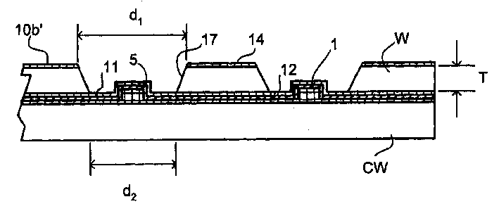
图3到8显示了本发明方法的一个示例中的步骤。首先,通过已知方式在晶片W的第一表面10a上蚀刻出正常标记(未示出)和倒转标记1-8,这些标记被SiO2的保护层11和Al的反射层12所覆盖,如作为沿图2中Y轴的局部剖视图的图3所示。然后衬底W被翻转,采用粘合层13将其粘结在载体衬底CW上。图4显示了粘结在载体衬底CW上的衬底W,其中第二表面10b处于最上方。Figures 3 to 8 show the steps in one example of the method of the invention. First, normal marks (not shown) and inversion marks 1-8 are etched in a known manner on the
如图5所示,晶片W被磨削至所需的厚度T,例如约为70微米,并且上表面10b’根据将形成于其上的器件的需要来精加工。As shown in Figure 5, the wafer W is ground to a desired thickness T, for example about 70 microns, and the
为了局部地蚀刻穿过第一衬底以显露出倒转标记1-8,首先例如通过沉积在第二表面10b’上覆盖一层氧化物14,如图6所示,并且覆盖一层抗蚀剂15,对抗蚀剂层15进行曝光以在倒转标记1-8之上形成敞开的初始蚀刻窗孔(primary flood window)16。由于初始蚀刻窗孔16比标记大很多,因此它们不必精确地定位,可以在采用粗略对准工具来定位标记之后进行用于形成窗孔16的曝光步骤,粗略对准工具例如为采用红外线的标记传感器,其可通过衬底W来检测倒转标记。In order to etch locally through the first substrate to reveal the inversion marks 1-8, a layer of
可通过干蚀刻RIE或湿蚀刻(含有HF的缓冲氧化物腐蚀)步骤来除去窗孔16中的氧化物层14,从而形成硬掩模,并进行采用为Si选出的蚀刻剂的深槽蚀刻来形成沟槽17。深槽蚀刻终止于SiO2层,因此沟槽17向下延伸到倒转初始标记1,5中,达到图8所示的位置。之后,可在与显露于沟槽17中的倒转标记1-8对准的情况下在第二表面10b’上形成器件层。沟槽的顶部宽度d1例如为1200微米,其足以保证其底部的宽度d2足够大,例如为1000微米,从而宽敞地容纳下标记1-8。然后在进行后续加工之前除去氧化物层14。The
粘合衬底的后续加工中的第一步骤是在晶片的现在处于最上方的第二表面10b’上印刷另外的标记,它们相对于所显露出的标记处于已知的位置。这些另外的标记可在第二表面的进一步加工中用于对准,它们比所显露出的标记方便得多。A first step in the subsequent processing of the bonded substrates is to print additional markings on the now uppermost
虽然在上文中介绍了本发明的特定实施例,然而应当理解,本发明可以不同于上述的方式来实施。此说明书并不意味限制了本发明。While specific embodiments of the invention have been described above, it should be understood that the invention may be practiced otherwise than as described above. This description is not meant to limit the invention.
Claims (11)
Applications Claiming Priority (2)
| Application Number | Priority Date | Filing Date | Title |
|---|---|---|---|
| EP02257846 | 2002-11-13 | ||
| EP02257846.2 | 2002-11-13 |
Publications (1)
| Publication Number | Publication Date |
|---|---|
| CN1501165A true CN1501165A (en) | 2004-06-02 |
Family
ID=32695568
Family Applications (1)
| Application Number | Title | Priority Date | Filing Date |
|---|---|---|---|
| CNA200310116131A Pending CN1501165A (en) | 2002-11-13 | 2003-11-12 | Device manufacturing method and device produced therefrom |
Country Status (6)
| Country | Link |
|---|---|
| US (1) | US7320847B2 (en) |
| JP (1) | JP2004165670A (en) |
| KR (1) | KR100585210B1 (en) |
| CN (1) | CN1501165A (en) |
| SG (1) | SG142129A1 (en) |
| TW (1) | TWI275912B (en) |
Cited By (2)
| Publication number | Priority date | Publication date | Assignee | Title |
|---|---|---|---|---|
| US7771899B2 (en) | 2006-09-29 | 2010-08-10 | Hynix Semiconductor Inc. | Method for repairing photomask pattern defects |
| CN114628403A (en) * | 2020-11-27 | 2022-06-14 | 京东方科技集团股份有限公司 | Display substrate mother board, preparation method thereof, display substrate and display device |
Families Citing this family (7)
| Publication number | Priority date | Publication date | Assignee | Title |
|---|---|---|---|---|
| KR101257960B1 (en) | 2004-06-04 | 2013-04-24 | 칼 짜이스 에스엠테 게엠베하 | System for measuring the image quality of an optical imaging system |
| JP4561265B2 (en) * | 2004-09-14 | 2010-10-13 | ソニー株式会社 | Back-illuminated solid-state imaging device and manufacturing method thereof |
| US20070269959A1 (en) * | 2006-05-16 | 2007-11-22 | Freeman John E | Method of aligning mask layers to buried features |
| US20080083818A1 (en) * | 2006-10-06 | 2008-04-10 | Asml Netherlands B.V. | Measuring the bonding of bonded substrates |
| NL1036308A1 (en) * | 2007-12-19 | 2009-06-22 | Asml Netherlands Bv | Lithographic method. |
| US12057332B2 (en) | 2016-07-12 | 2024-08-06 | Ayar Labs, Inc. | Wafer-level etching methods for planar photonics circuits and devices |
| US11101617B2 (en) | 2018-07-16 | 2021-08-24 | Ayar Labs, Inc. | Wafer-level handle replacement |
Family Cites Families (9)
| Publication number | Priority date | Publication date | Assignee | Title |
|---|---|---|---|---|
| US4737033A (en) * | 1986-10-07 | 1988-04-12 | General Electric Co. | Alignment key and method of making the same |
| JP3175188B2 (en) * | 1991-05-10 | 2001-06-11 | ソニー株式会社 | Method of forming alignment mark |
| US5436173A (en) * | 1993-01-04 | 1995-07-25 | Texas Instruments Incorporated | Method for forming a semiconductor on insulator device |
| JP3239976B2 (en) | 1994-09-30 | 2001-12-17 | 株式会社東芝 | Alignment mark, method of manufacturing semiconductor device, and semiconductor device |
| US5898227A (en) * | 1997-02-18 | 1999-04-27 | International Business Machines Corporation | Alignment targets having enhanced contrast |
| JP2000232044A (en) | 1999-02-09 | 2000-08-22 | Nec Corp | Semiconductor device and its manufacture |
| EP1148546A1 (en) | 2000-04-19 | 2001-10-24 | Infineon Technologies AG | Method for alignment of structures on a semiconductor substrate |
| US6335214B1 (en) * | 2000-09-20 | 2002-01-01 | International Business Machines Corporation | SOI circuit with dual-gate transistors |
| KR100579603B1 (en) * | 2001-01-15 | 2006-05-12 | 에이에스엠엘 네델란즈 비.브이. | Lithographic Apparatus |
-
2003
- 2003-11-06 SG SG200306596-8A patent/SG142129A1/en unknown
- 2003-11-12 TW TW092131674A patent/TWI275912B/en not_active IP Right Cessation
- 2003-11-12 CN CNA200310116131A patent/CN1501165A/en active Pending
- 2003-11-12 JP JP2003382650A patent/JP2004165670A/en active Pending
- 2003-11-12 US US10/705,218 patent/US7320847B2/en not_active Expired - Fee Related
- 2003-11-13 KR KR1020030080085A patent/KR100585210B1/en not_active Expired - Fee Related
Cited By (3)
| Publication number | Priority date | Publication date | Assignee | Title |
|---|---|---|---|---|
| US7771899B2 (en) | 2006-09-29 | 2010-08-10 | Hynix Semiconductor Inc. | Method for repairing photomask pattern defects |
| CN114628403A (en) * | 2020-11-27 | 2022-06-14 | 京东方科技集团股份有限公司 | Display substrate mother board, preparation method thereof, display substrate and display device |
| CN114628403B (en) * | 2020-11-27 | 2025-02-07 | 京东方科技集团股份有限公司 | Display substrate motherboard and preparation method thereof, display substrate and display device |
Also Published As
| Publication number | Publication date |
|---|---|
| US20040142256A1 (en) | 2004-07-22 |
| TWI275912B (en) | 2007-03-11 |
| KR100585210B1 (en) | 2006-05-30 |
| SG142129A1 (en) | 2008-05-28 |
| TW200523681A (en) | 2005-07-16 |
| KR20040042860A (en) | 2004-05-20 |
| US7320847B2 (en) | 2008-01-22 |
| JP2004165670A (en) | 2004-06-10 |
Similar Documents
| Publication | Publication Date | Title |
|---|---|---|
| CN1313886C (en) | Device manufacturing method | |
| JP4463843B2 (en) | Lithographic apparatus and device manufacturing method | |
| JP3693654B2 (en) | Calibration method, calibration substrate, lithographic apparatus and device manufacturing method | |
| TWI424288B (en) | Lithographic apparatus and device manufacturing method | |
| CN101923285B (en) | Lithographic method and arrangement | |
| KR20050065390A (en) | Method of measurement, method for providing alignment marks, and device manufacturing method | |
| CN1501174A (en) | Method for detecting mask defect, computer program and reference substrate | |
| JP2006054460A (en) | Positioning-mark providing method, substrate-positioning method, device manufacturing method, computer program, and device | |
| KR100734589B1 (en) | Substrate table, method of measuring a position of a substrate and a lithographic apparatus | |
| JP4520429B2 (en) | Application of two-dimensional photonic crystals to alignment equipment | |
| CN1501165A (en) | Device manufacturing method and device produced therefrom | |
| JP4299262B2 (en) | Lithographic apparatus and device manufacturing method | |
| JP2006186367A (en) | System and method for forming bonded substrate and bonded substrate product | |
| JP4658004B2 (en) | Device manufacturing method | |
| JP4435760B2 (en) | Device manufacturing method | |
| TW201826342A (en) | Component manufacturing method | |
| EP1420449A1 (en) | Device manufacturing method with reversed alignment markers | |
| CN1495536A (en) | Method for aligning substrates, computer program, method for manufacturing devices and devices made therefrom | |
| EP1469355B1 (en) | Device manufacturing method | |
| JP4972126B2 (en) | Lithographic apparatus, composite material, movable component and manufacturing method | |
| KR20070035531A (en) | Moiré pattern generating apparatus and method for measuring the position of the substrate |
Legal Events
| Date | Code | Title | Description |
|---|---|---|---|
| C06 | Publication | ||
| PB01 | Publication | ||
| C10 | Entry into substantive examination | ||
| SE01 | Entry into force of request for substantive examination | ||
| C02 | Deemed withdrawal of patent application after publication (patent law 2001) | ||
| WD01 | Invention patent application deemed withdrawn after publication |