CN1499477A - A Method of Quickly Processing Image Data and Improving Image Definition - Google Patents
A Method of Quickly Processing Image Data and Improving Image Definition Download PDFInfo
- Publication number
- CN1499477A CN1499477A CNA031483372A CN03148337A CN1499477A CN 1499477 A CN1499477 A CN 1499477A CN A031483372 A CNA031483372 A CN A031483372A CN 03148337 A CN03148337 A CN 03148337A CN 1499477 A CN1499477 A CN 1499477A
- Authority
- CN
- China
- Prior art keywords
- resolution
- virtual screen
- image data
- area
- mask
- Prior art date
- Legal status (The legal status is an assumption and is not a legal conclusion. Google has not performed a legal analysis and makes no representation as to the accuracy of the status listed.)
- Pending
Links
Images


Classifications
-
- G—PHYSICS
- G09—EDUCATION; CRYPTOGRAPHY; DISPLAY; ADVERTISING; SEALS
- G09G—ARRANGEMENTS OR CIRCUITS FOR CONTROL OF INDICATING DEVICES USING STATIC MEANS TO PRESENT VARIABLE INFORMATION
- G09G3/00—Control arrangements or circuits, of interest only in connection with visual indicators other than cathode-ray tubes
- G09G3/20—Control arrangements or circuits, of interest only in connection with visual indicators other than cathode-ray tubes for presentation of an assembly of a number of characters, e.g. a page, by composing the assembly by combination of individual elements arranged in a matrix no fixed position being assigned to or needed to be assigned to the individual characters or partial characters
-
- G—PHYSICS
- G09—EDUCATION; CRYPTOGRAPHY; DISPLAY; ADVERTISING; SEALS
- G09G—ARRANGEMENTS OR CIRCUITS FOR CONTROL OF INDICATING DEVICES USING STATIC MEANS TO PRESENT VARIABLE INFORMATION
- G09G5/00—Control arrangements or circuits for visual indicators common to cathode-ray tube indicators and other visual indicators
- G09G5/02—Control arrangements or circuits for visual indicators common to cathode-ray tube indicators and other visual indicators characterised by the way in which colour is displayed
- G09G5/04—Control arrangements or circuits for visual indicators common to cathode-ray tube indicators and other visual indicators characterised by the way in which colour is displayed using circuits for interfacing with colour displays
-
- G—PHYSICS
- G09—EDUCATION; CRYPTOGRAPHY; DISPLAY; ADVERTISING; SEALS
- G09G—ARRANGEMENTS OR CIRCUITS FOR CONTROL OF INDICATING DEVICES USING STATIC MEANS TO PRESENT VARIABLE INFORMATION
- G09G3/00—Control arrangements or circuits, of interest only in connection with visual indicators other than cathode-ray tubes
- G09G3/20—Control arrangements or circuits, of interest only in connection with visual indicators other than cathode-ray tubes for presentation of an assembly of a number of characters, e.g. a page, by composing the assembly by combination of individual elements arranged in a matrix no fixed position being assigned to or needed to be assigned to the individual characters or partial characters
- G09G3/22—Control arrangements or circuits, of interest only in connection with visual indicators other than cathode-ray tubes for presentation of an assembly of a number of characters, e.g. a page, by composing the assembly by combination of individual elements arranged in a matrix no fixed position being assigned to or needed to be assigned to the individual characters or partial characters using controlled light sources
-
- G—PHYSICS
- G09—EDUCATION; CRYPTOGRAPHY; DISPLAY; ADVERTISING; SEALS
- G09G—ARRANGEMENTS OR CIRCUITS FOR CONTROL OF INDICATING DEVICES USING STATIC MEANS TO PRESENT VARIABLE INFORMATION
- G09G2320/00—Control of display operating conditions
- G09G2320/06—Adjustment of display parameters
- G09G2320/0666—Adjustment of display parameters for control of colour parameters, e.g. colour temperature
-
- G—PHYSICS
- G09—EDUCATION; CRYPTOGRAPHY; DISPLAY; ADVERTISING; SEALS
- G09G—ARRANGEMENTS OR CIRCUITS FOR CONTROL OF INDICATING DEVICES USING STATIC MEANS TO PRESENT VARIABLE INFORMATION
- G09G2340/00—Aspects of display data processing
- G09G2340/04—Changes in size, position or resolution of an image
- G09G2340/0407—Resolution change, inclusive of the use of different resolutions for different screen areas
-
- G—PHYSICS
- G09—EDUCATION; CRYPTOGRAPHY; DISPLAY; ADVERTISING; SEALS
- G09G—ARRANGEMENTS OR CIRCUITS FOR CONTROL OF INDICATING DEVICES USING STATIC MEANS TO PRESENT VARIABLE INFORMATION
- G09G3/00—Control arrangements or circuits, of interest only in connection with visual indicators other than cathode-ray tubes
- G09G3/20—Control arrangements or circuits, of interest only in connection with visual indicators other than cathode-ray tubes for presentation of an assembly of a number of characters, e.g. a page, by composing the assembly by combination of individual elements arranged in a matrix no fixed position being assigned to or needed to be assigned to the individual characters or partial characters
- G09G3/2007—Display of intermediate tones
- G09G3/2074—Display of intermediate tones using sub-pixels
-
- G—PHYSICS
- G09—EDUCATION; CRYPTOGRAPHY; DISPLAY; ADVERTISING; SEALS
- G09G—ARRANGEMENTS OR CIRCUITS FOR CONTROL OF INDICATING DEVICES USING STATIC MEANS TO PRESENT VARIABLE INFORMATION
- G09G3/00—Control arrangements or circuits, of interest only in connection with visual indicators other than cathode-ray tubes
- G09G3/20—Control arrangements or circuits, of interest only in connection with visual indicators other than cathode-ray tubes for presentation of an assembly of a number of characters, e.g. a page, by composing the assembly by combination of individual elements arranged in a matrix no fixed position being assigned to or needed to be assigned to the individual characters or partial characters
- G09G3/22—Control arrangements or circuits, of interest only in connection with visual indicators other than cathode-ray tubes for presentation of an assembly of a number of characters, e.g. a page, by composing the assembly by combination of individual elements arranged in a matrix no fixed position being assigned to or needed to be assigned to the individual characters or partial characters using controlled light sources
- G09G3/28—Control arrangements or circuits, of interest only in connection with visual indicators other than cathode-ray tubes for presentation of an assembly of a number of characters, e.g. a page, by composing the assembly by combination of individual elements arranged in a matrix no fixed position being assigned to or needed to be assigned to the individual characters or partial characters using controlled light sources using luminous gas-discharge panels, e.g. plasma panels
Landscapes
- Engineering & Computer Science (AREA)
- Physics & Mathematics (AREA)
- Computer Hardware Design (AREA)
- General Physics & Mathematics (AREA)
- Theoretical Computer Science (AREA)
- Control Of Indicators Other Than Cathode Ray Tubes (AREA)
- Television Systems (AREA)
- Controls And Circuits For Display Device (AREA)
- Transforming Electric Information Into Light Information (AREA)
- Video Image Reproduction Devices For Color Tv Systems (AREA)
Abstract
提供处理图像数据,产生输出图像数据,驱动显示板的一种方法。在这种方法中,按照显示板的分辨率设置输入图像数据的新分辨率。按照为输入图像数据设置的新分辨率,将第一个虚拟屏幕划分成多个像素区域。将具有显示板的子像素阵列结构的第二个虚拟屏幕重叠在第一个虚拟屏幕上。将比重叠的第二个虚拟屏幕上的子像素区域宽的一个掩模放置在每个子像素区域上。获得和设置包括在每个掩模中包括的第一个虚拟屏幕上的每个像素部分的面积与掩模的面积的面积比。将新分辨率和面积比应用于显示板的驱动装置。将具有原始分辨率的输入图像数据转换成具有新分辨率的图像数据。产生包括在每个掩模中第一个虚拟屏幕上每个像素部分的面积与转换过的像素区域的图像数据相乘得到的结果的和,作为对应于掩模的子像素的输出图像数据。
Provides a method for processing image data, generating output image data, and driving a display panel. In this method, the new resolution of the input image data is set according to the resolution of the display panel. Divides the first virtual screen into regions of pixels according to the new resolution set for the input image data. A second virtual screen having a sub-pixel array structure of the display panel is superimposed on the first virtual screen. A mask wider than the sub-pixel area on the overlapping second virtual screen is placed on each sub-pixel area. Gets and sets the area ratio of the area of each pixel portion on the first virtual screen included in each mask to the area of the mask. Apply the new resolution and area ratio to the driving device of the display panel. Convert input image data with original resolution to image data with new resolution. A sum of results obtained by multiplying the area of each pixel portion on the first virtual screen in each mask by the image data of the converted pixel area is generated as output image data corresponding to sub-pixels of the mask.
Description
优先权声明priority statement
根据35美国第119节(claims all benefits accruing under 35U.S.C.§119 from an application),本申请要求享受2002年11月4日向韩国工业知识产权办公室提交的标题为“快速处理图像数据提高图像可重现性的方法”的第2002-67967号申请的优先权,同时将该申请引入作为参考。According to Section 119 of 35 U.S. (claims all benefits accruing under 35 U.S.C. § 119 from an application), this application claims to enjoy the title of "Rapid Processing of Image Data to Improve Image Reproducibility" submitted to the Korean Industrial Intellectual Property Office on November 4, 2002. Priority of Application No. 2002-67967 of "Present Method", which application is also incorporated by reference.
技术领域technical field
本发明涉及处理图像数据的一种方法,具体而言,涉及处理输入的图像数据,产生输出图像数据,驱动显示板的一种方法。The present invention relates to a method for processing image data, in particular, relates to a method for processing input image data, generating output image data, and driving a display panel.
技术背景technical background
处理图像数据的一般方法包括根据输入图像数据分辨率划分成多个像素区域的第一个虚拟屏幕,以及具有显示板子像素阵列的第二个虚拟屏幕。第一个虚拟屏幕包括红色子像素区域、绿色子像素区域和蓝色子像素区域。A general method of processing image data includes a first virtual screen divided into a plurality of pixel regions according to the resolution of input image data, and a second virtual screen having a display panel sub-pixel array. The first virtual screen includes a red sub-pixel area, a green sub-pixel area and a blue sub-pixel area.
输入的图像数据只有单元像素的位置信息,而没有构成这个单元像素的子像素的位置信息,也就是红色子像素、绿色子像素和蓝色子像素的信息。但是,所有显示板上不同像素区域中子像素的位置不同。除此以外,对于两个相邻像素,红色子像素之间的距离,绿色子像素之间的距离以及蓝色子像素之间的距离互不相同。因此会降低显示板上显示的图像的清晰度。The input image data only has the position information of the unit pixel, but does not have the position information of the sub-pixels constituting the unit pixel, that is, the information of the red sub-pixel, the green sub-pixel and the blue sub-pixel. However, the positions of the sub-pixels in different pixel areas are different on all display panels. Besides, for two adjacent pixels, the distance between the red sub-pixels, the distance between the green sub-pixels and the distance between the blue sub-pixels are different from each other. Therefore, the sharpness of the image displayed on the display panel is reduced.
Benzschawel等等的第5341153号美国专利“显示多色图像的方法和装置”公开了与图像清晰度有关的一种技术。按照这一技术,具有高分辨率的输入图像数据被直接重叠在低分辨率的显示板上。由于子像素阵列的结构,这项技术不能从根本上解决显示板上图像的清晰度问题。此外,由于输入的图像数据转换操作是针对显示板上所有子像素一个一个进行的,因此,显示速度下降了。US Patent No. 5,341,153 "Method and Apparatus for Displaying Multicolor Images" by Benzschawel et al. discloses a technique related to image sharpness. According to this technique, input image data having a high resolution is directly superimposed on a display panel having a low resolution. Due to the structure of the sub-pixel array, this technology cannot fundamentally solve the problem of image clarity on the display panel. In addition, since the input image data conversion operation is performed one by one for all sub-pixels on the display panel, the display speed decreases.
发明内容Contents of the invention
因此,本发明的一个目的是提供一种方法用来处理图像数据,用最少的输入图像数据转换操作,从根本上解决显示板上子像素结构带来的图像清晰度问题。Therefore, it is an object of the present invention to provide a method for processing image data that fundamentally solves the image definition problem caused by the sub-pixel structure on the display panel with the least input image data conversion operations.
另一个目的是通过为输入图像数据提供一个新分辨率来处理图像数据,设置这个新分辨率的目的是使得具有相同面积比结构的掩模数量最多,因而使得使用的掩模的数量最少,面积比乘以转换过的图像数据的次数最小,从而提高显示速度,降低需要的存储容量。Another purpose is to process the image data by providing a new resolution for the input image data, the purpose of setting this new resolution is to maximize the number of masks with the same area ratio structure, thus minimizing the number of masks used, the area The times of multiplication by the converted image data are minimized, thereby increasing the display speed and reducing the required storage capacity.
再一个目的是让显示板上每个子像素都与第一个虚拟屏幕上它相邻像素的数据联系起来,从能够从根本上解决图像再现过程中显示板的子像素阵列结构带来的问题。Another purpose is to link each sub-pixel on the display panel with the data of its adjacent pixels on the first virtual screen, so as to fundamentally solve the problems caused by the sub-pixel array structure of the display panel in the process of image reproduction.
还有一个目的是校正数据处理过程中可能出现的颜色偏差。Yet another purpose is to correct color biases that may occur during data processing.
为了上述目的和其它目的,根据本发明的一个方面,提供一种方法用来处理图像数据,产生输出图像数据,驱动显示板。在这种方法中,按照显示板的分辨率为输入图像数据设置一个新分辨率。按照为输入的图像数据设置的新分辨率将第一个虚拟屏幕划分成多个像素区域。具有显示板子像素阵列结构的第二个虚拟屏幕重叠在第一个虚拟屏幕上。在每个子像素区域上放上比重叠的第二个虚拟屏幕上子像素面积大的一个掩模。获得和设置第一个虚拟屏幕上包括在每个掩模中的每个子像素部分的面积与掩模的面积的面积比。将新分辨率和面积比用于驱动显示板的驱动装置。具有原始分辨率的输入图像数据被转换成具有新、增强了的分辨率的图像数据。产生将第一个虚拟屏幕上包括在每个掩模中每个像素部分的面积的面积比乘以像素区域转换过的图像数据得到的结果的和,作为对应于掩模的子像素的输出图像数据。To achieve the above and other objects, according to an aspect of the present invention, there is provided a method for processing image data, generating output image data, and driving a display panel. In this method, a new resolution is set for input image data according to the resolution of the display panel. Divides the first virtual screen into pixel regions according to the new resolution set for the input image data. A second virtual screen with a display panel sub-pixel array structure is superimposed on the first virtual screen. A mask larger than the sub-pixel area on the overlapping second virtual screen is placed on each sub-pixel area. The area ratio of the area of each sub-pixel portion included in each mask on the first virtual screen to the area of the mask is obtained and set. The new resolution and area ratio are used in the driving device for driving the display panel. Input image data with original resolution is converted into image data with new, enhanced resolution. producing the sum of the results obtained by multiplying the area ratio of the area of each pixel portion included in each mask on the first virtual screen by the pixel area-converted image data, as an output image corresponding to the subpixel of the mask data.
本发明中处理图像数据的方法具有以下效果。The method of processing image data in the present invention has the following effects.
首先,可以给输入的图像数据设置一个新分辨率,以便使具有相同面积比结构的掩模的数量最多。因此,要使用的掩模的数量最少,于是面积比乘以转换过的图像数据的次数最少,从而提高显示速度,减少必需的存储容量。First, a new resolution can be set to the input image data in order to maximize the number of masks having structures with the same area ratio. Therefore, the number of masks to be used is minimized, and thus the number of times the area ratio is multiplied by the converted image data is minimized, thereby increasing the display speed and reducing the necessary storage capacity.
其次,显示板上每个子像素都与第一个虚拟屏幕上和它相邻的像素的数据有关,因此再现图像的时候因为显示板子像素阵列结构带来的问题能够从根本上加以解决。Secondly, each sub-pixel on the display board is related to the data of its adjacent pixels on the first virtual screen, so the problems caused by the sub-pixel array structure of the display board can be fundamentally solved when reproducing images.
附图说明Description of drawings
通过阅读以下详细介绍,同时参考附图,就会对本发明的优点有更加全面的了解,在这些附图中,相似的引用符号表示相同或者相似的部件,其中:A more complete appreciation of the advantages of the present invention will be obtained by reading the following detailed description, while referring to the accompanying drawings, in which like reference numerals indicate the same or similar parts, in which:
图1说明处理图像数据的传统方法;Figure 1 illustrates a conventional approach to processing image data;
图2说明划分子像素的方法;FIG. 2 illustrates a method of dividing sub-pixels;
图3说明本发明中图像数据处理方法的原理;Fig. 3 illustrates the principle of image data processing method among the present invention;
图4是本发明一个实施方案中处理图像数据的方法流程图;Fig. 4 is a flow chart of a method for processing image data in one embodiment of the present invention;
图5给出从图4所示步骤S2得到的第一个虚拟屏幕的一个实例;Fig. 5 provides an example of the first virtual screen obtained from step S2 shown in Fig. 4;
图6给出输入图像数据新分辨率与显示板分辨率之比为1∶1的时候,从图4所示的步骤S3得到的虚拟屏幕的一个重叠实例;Fig. 6 provides when the ratio of the new resolution of the input image data and the resolution of the display panel is 1: 1, an overlapping example of the virtual screen obtained from step S3 shown in Fig. 4;
图7给出输入图像数据新分辨率与显示板分辨率之比为1.5∶1的时候,从图4所示的步骤S3得到的虚拟屏幕的一个重叠实例;Fig. 7 provides an overlapping example of the virtual screen obtained from step S3 shown in Fig. 4 when the ratio of the new resolution of the input image data to the resolution of the display panel is 1.5:1;
图8A给出输入图像数据新分辨率与显示板分辨率之比为1.5∶1的时候,从图4所示的步骤S3得到的虚拟屏幕的一个重叠实例,在这个虚拟屏幕上将四边形的掩模放在每个蓝色子像素区域上;Fig. 8A shows an overlapping example of the virtual screen obtained from step S3 shown in Fig. 4 when the ratio of the new resolution of the input image data to the resolution of the display panel is 1.5:1, and the quadrilateral mask is placed on the virtual screen Die on each blue sub-pixel area;
图8B画出了图8A所示阴影掩模区域的一个放大图;Figure 8B depicts an enlarged view of the shadow mask area shown in Figure 8A;
图9A画出了输入图像数据新分辨率与显示板分辨率之比为1.5∶1的时候,从图4所示步骤S4得到的虚拟屏幕的一个重叠实例,在这个虚拟屏幕上将一个六边形的掩模放在每个蓝色子像素区域上;Fig. 9A has drawn when the ratio of the new resolution of input image data and the resolution of display panel is 1.5: 1, an overlapping instance of the virtual screen obtained from step S4 shown in Fig. 4, a hexagonal A shaped mask is placed on each blue sub-pixel area;
图9B画出了图9A所示阴影掩模区域的一个放大图,以此来说明图4中的步骤S5所使用的另一个算法;FIG. 9B shows an enlarged view of the shadow mask region shown in FIG. 9A to illustrate another algorithm used in step S5 in FIG. 4;
图10A画出了输入图像数据新分辨率与显示板分辨率之比为1.5∶1的时候,从图4所示步骤S4得到的虚拟屏幕的一个重叠实例,在这个虚拟屏幕上将一个圆形掩模放在每个蓝色子像素区域上;Fig. 10A has drawn when the ratio of the new resolution of input image data and display board resolution is 1.5: 1, an overlapping instance of the virtual screen obtained from step S4 shown in Fig. 4, on this virtual screen a circular A mask is placed over each blue sub-pixel area;
图10B画出了图10A所示阴影掩模区域的一个放大图,以此来说明图4中的步骤S5所使用的再一个算法;FIG. 10B has drawn an enlarged view of the shadow mask region shown in FIG. 10A to illustrate another algorithm used in step S5 in FIG. 4;
图11画出了输入图像数据新分辨率与显示板分辨率之比为1.4∶1的时候,第二个虚拟屏幕上的子像素区域,与第一个虚拟屏幕上的单元像素区域相比,位于不同的水平和垂直位置上;Figure 11 shows when the ratio of the new resolution of the input image data to the resolution of the display panel is 1.4:1, the sub-pixel area on the second virtual screen is compared with the unit pixel area on the first virtual screen, at different horizontal and vertical positions;
图12画出了输入图像数据新分辨率与显示板分辨率之比为1.5∶1的时候,它们位于第一个虚拟屏幕上不同单元像素区域中不同的水平和垂直位置上;Figure 12 shows that when the ratio of the new resolution of the input image data to the resolution of the display panel is 1.5:1, they are located at different horizontal and vertical positions in different unit pixel areas on the first virtual screen;
图13A说明显示板的子像素区域有一个德尔塔结构的时候,不同水平位置数量与水平分辨率比之间的关系;13A illustrates the relationship between the number of different horizontal positions and the horizontal resolution ratio when the sub-pixel area of the display panel has a delta structure;
图13B说明显示板的子像素区域有一个德尔塔结构的时候,不同垂直位置数量与垂直分辨率比之间的关系;FIG. 13B illustrates the relationship between the number of different vertical positions and the vertical resolution ratio when the sub-pixel area of the display panel has a delta structure;
图14说明显示板子像素区域具有条形结构的时候,掩模数量与分辨率比之间的关系;Figure 14 illustrates the relationship between the number of masks and the resolution ratio when the sub-pixel region of the display panel has a strip structure;
图15说明显示板子像素区域具有德尔塔结构的时候,掩模数量与分辨率比之间的关系;Figure 15 illustrates the relationship between the number of masks and the resolution ratio when the sub-pixel region of the display panel has a delta structure;
图1A说明第一个虚拟屏幕上像素区域中心线是第二个虚拟屏幕上子像素区域中心线的情况;Fig. 1A illustrates the situation that the center line of the pixel area on the first virtual screen is the center line of the sub-pixel area on the second virtual screen;
图16B说明第一个虚拟屏幕上像素区域中心线不是第二个虚拟屏幕上子像素区域中心线的情况;Fig. 16B illustrates the situation that the center line of the pixel area on the first virtual screen is not the center line of the sub-pixel area on the second virtual screen;
图17~19给出了包括利用了本发明的技术的显示器的一些装置实例。Figures 17-19 give some examples of devices including displays utilizing the techniques of the present invention.
具体实施方式Detailed ways
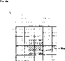
图1说明处理图像数据的一般方法的原理。符号VSS表示第一个虚拟屏幕,按照输入图像数据的分辨率将它划分成多个像素区域。符号VDS表示有一个显示板的子像素阵列的第二个虚拟屏幕。在第二个虚拟屏幕VDS中,中心画上了圆圈的区域是红色子像素区域,中心画上了方块的区域是绿色子像素区域,中心画上了钻石符号的区域是蓝色子像素区域。Figure 1 illustrates the principle of a general method for processing image data. Symbol V SS represents the first virtual screen, which is divided into a plurality of pixel regions according to the resolution of the input image data. The notation V DS denotes a second virtual screen with an array of sub-pixels of the display panel. In the second virtual screen VDS , the area with a circle in the center is a red sub-pixel area, the area with a square in the center is a green sub-pixel area, and the area with a diamond symbol in the center is a blue sub-pixel area .
参考图1,输入的图像数据只有单元像素的位置信息,而没有构成单元像素的子像素的位置信息,也就是红色子像素、绿色子像素和蓝色子像素的位置信息。但是,所有显示板上不同像素区域中子像素的位置不同。除此以外,对于两个相邻像素,红色子像素之间的距离、绿色子像素之间的距离和蓝色子像素之间的距离互不相同。因此,显示板上显示的图像的清晰度降低了。Referring to FIG. 1 , the input image data only has the position information of the unit pixel, but does not have the position information of the sub-pixels constituting the unit pixel, that is, the position information of the red sub-pixel, the green sub-pixel and the blue sub-pixel. However, the positions of the sub-pixels in different pixel areas are different on all display panels. Besides, for two adjacent pixels, the distance between the red sub-pixels, the distance between the green sub-pixels and the distance between the blue sub-pixels are different from each other. Therefore, the sharpness of the image displayed on the display panel is lowered.
参考图2,划分出子像素方法包括检查输入信号分辨率(步骤A10)。检查了输入信号分辨率以后,就对划分出最佳子像素的比值之一进行输入分辨率转换(步骤A12)。在步骤A12以后确定掩模形状(步骤A14)。还要确定掩模相对于第一个虚拟屏幕的放置位置(步骤A16)。获得与第一个虚拟屏幕划分的掩模成正比的表格(步骤A18)。按照表格计算子像素值(步骤A20)。最后检查颜色看有没有偏差,同时检查输出图像(步骤A22)。Referring to FIG. 2, the method of dividing into sub-pixels includes checking an input signal resolution (step A10). After checking the input signal resolution, input resolution conversion is performed on one of the ratios that divides the best sub-pixels (step A12). After step A12, the mask shape is determined (step A14). Also determine the placement position of the mask relative to the first virtual screen (step A16). A table proportional to the mask of the first virtual screen division is obtained (step A18). Sub-pixel values are calculated according to the table (step A20). Finally, check the color to see if there is any deviation, and check the output image at the same time (step A22).
图3说明本发明中处理图像数据的方法的原理。符号VSS表示第一个虚拟屏幕,按照输入图像数据的新分辨率,它被划分成多个像素区域。符号VDS表示显示板具有子像素阵列的第二个虚拟屏幕。在第二个虚拟屏幕VDS上,中心有圆圈的区域是红色子像素区域,中心有方形的是绿色子像素区域,中心有钻石符号的区域是蓝色子像素区域。Fig. 3 illustrates the principle of the method of processing image data in the present invention. The symbol V SS represents the first virtual screen, which is divided into a plurality of pixel areas according to the new resolution of the input image data. The symbol V DS denotes a second virtual screen of the display panel with an array of sub-pixels. On the second virtual screen VDS , the area with a circle in the center is a red sub-pixel area, the area with a square in the center is a green sub-pixel area, and the area with a diamond symbol in the center is a blue sub-pixel area.
图4说明本发明中一个实施方案里处理图像数据的方法。在图4中,步骤S1~S5表示制造显示驱动装置的时候设置分辨率和面积比的步骤。下面将参考图3和图4从原理上介绍按照本发明的一个实施方案处理图像数据的方法。Figure 4 illustrates a method of processing image data in one embodiment of the present invention. In FIG. 4, steps S1 to S5 represent the steps of setting the resolution and the area ratio when manufacturing the display driving device. A method for processing image data according to an embodiment of the present invention will be described in principle below with reference to FIGS. 3 and 4 .
在步骤S1中按照显示板的分辨率设置输入图像数据的新分辨率。在这里设置新的水平分辨率和新的垂直分辨率。按照显示板的水平分辨率来设置输入图像数据新的水平分辨率,按照显示板的垂直分辨率设置输入图像数据新的垂直分辨率。The new resolution of the input image data is set in step S1 according to the resolution of the display panel. Set the new horizontal resolution and the new vertical resolution here. The new horizontal resolution of the input image data is set according to the horizontal resolution of the display panel, and the new vertical resolution of the input image data is set according to the vertical resolution of the display panel.
在步骤S2中按照输入图像数据的新分辨率将第一个虚拟屏幕VSS划分成多个像素区域。在步骤S3中将具有显示板子像素阵列结构的第二个虚拟屏幕VDS重叠在第一个虚拟屏幕VSS上。在步骤S4中,将一个掩模放在显示板的每个单元区域内,这个掩模比虚拟屏幕VDS~VSS重叠位置上显示板每个子像素的区域宽。同样,这个掩模最好不包括下一个相同颜色的子像素。例如,如果掩模包括第一种颜色的子像素,这个掩模就不应该接触或者包括具有第一种颜色的下一个子像素。作为另一个实例,这个掩模可以只包括一个子像素颜色。在步骤S5中获得和设置一个面积比表,它说明每个掩模中第一个虚拟屏幕VSS每个像素部分的面积与掩模的面积之间的面积比。在步骤S6中,将步骤S1中设置的分辨率以及步骤S5中设置的面积比表应用于显示板的驱动装置,转换输入图像数据,从而使输入图像数据的原始分辨率变成步骤S1中设置的新分辨率,然后产生每个掩模中每个像素部分的面积与掩模面积的比值与转换后图像数据的乘积的和,作为对应于掩模的子像素的输出图像数据。换句话说,显示板的每个子像素都与第一个虚拟屏幕上它的相邻像素的数据有关。因此,如图3所示,可以校正第一个屏幕VSS的输入图像数据,以适合于显示板子像素阵列的结构,从而从根本上解决显示板子像素阵列结构带来的图像清晰度问题。In step S2, the first virtual screen V SS is divided into a plurality of pixel regions according to the new resolution of the input image data. In step S3, the second virtual screen V DS having the sub-pixel array structure of the display panel is superimposed on the first virtual screen V SS . In step S4, a mask is placed in each unit area of the display panel, and the mask is wider than the area of each sub-pixel of the display panel at the overlapping positions of virtual screens V DS -V SS . Again, this mask preferably excludes the next sub-pixel of the same color. For example, if a mask includes a subpixel of a first color, this mask should not touch or include the next subpixel of the first color. As another example, this mask may include only one subpixel color. An area ratio table indicating the area ratio between the area of each pixel portion of the first virtual screen V SS in each mask and the area of the mask is obtained and set in step S5. In step S6, the resolution set in step S1 and the area ratio table set in step S5 are applied to the driving device of the display panel, and the input image data is converted so that the original resolution of the input image data becomes the one set in step S1 , and then produce the sum of the product of the ratio of the area of each pixel portion in each mask to the mask area and the converted image data as output image data corresponding to the sub-pixels of the mask. In other words, each sub-pixel of the display panel is associated with the data of its neighbor pixels on the first virtual screen. Therefore, as shown in FIG. 3 , the input image data of the first screen V SS can be corrected to be suitable for the structure of the sub-pixel array of the display panel, thereby fundamentally solving the problem of image definition caused by the structure of the sub-pixel array of the display panel.
另外,在步骤S1中,设置输入图像数据的新分辨率,使得具有步骤S5中相同面积比结构的掩模的数量最多,从而减少步骤S4中使用的掩模的数量。因此,能够减少面积比与转换后图像数据相乘的次数。In addition, in step S1, the new resolution of the input image data is set such that the number of masks having the same area ratio structure in step S5 is the largest, thereby reducing the number of masks used in step S4. Therefore, the number of times the area ratio is multiplied by the converted image data can be reduced.
参考图5,执行图4所示步骤S2的时候,按照为输入图像数据设置的新分辨率将第一个虚拟屏幕VSS划分成多个像素区域VP11~VP6(10)。Referring to FIG. 5 , when step S2 shown in FIG. 4 is executed, the first virtual screen V SS is divided into a plurality of pixel areas VP 11 -VP 6(10) according to the new resolution set for the input image data.
图6给出输入图像数据的新分辨率与显示板分辨率之间的比值是1∶1的时候,从图14所示的步骤S3得到的虚拟屏幕VDS~VSS的一个重叠实例。在图6中,符号CR12~CR33表示红色子像素区域,符号CG11~CG33表示绿色子像素区域,符号CB11~CB33表示蓝色于像素区域。参考图6,和显示板子像素阵列结构一样具有德尔塔结构的第二个虚拟屏幕重叠在第一个虚拟屏幕VSS上。换句话说,划分成子像素区域CG11~CG33的多个子像素区域重叠在划分成多个子像素区域VP15~VP47的第一个虚拟屏幕VSS上。FIG. 6 shows an overlapping example of the virtual screens V DS ˜ V SS obtained from step S3 shown in FIG. 14 when the ratio between the new resolution of the input image data and the resolution of the display panel is 1:1. In FIG. 6 , symbols CR 12 to CR 33 represent red sub-pixel regions, symbols CG 11 to CG 33 represent green sub-pixel regions, and symbols CB 11 to CB 33 represent blue sub-pixel regions. Referring to FIG. 6 , a second virtual screen having a delta structure like the sub-pixel array structure of the display panel is superimposed on the first virtual screen V SS . In other words, a plurality of sub-pixel regions divided into sub-pixel regions CG 11 -CG 33 overlap on the first virtual screen V SS divided into a plurality of sub-pixel regions VP 15 -VP 47 .
图7给出了输入图像数据的新分辨率与显示板分辨率之间的比值为1.5的时候,从图4所示步骤S3得到的虚拟屏幕VDS~VSS的一个重叠实例。在图7中,实线划定的区域是第一个虚拟屏幕VSS上的像素区域,虚线划定的区域是第二个虚拟屏幕VDS上的子像素区域。在第二个虚拟屏幕VDS上,中心画上了圆圈的区域是红色子像素区域,中心画上了方框的区域是绿色子像素区域,中心画上了钻石符号的区域是蓝色子像素区域。FIG. 7 shows an overlapping example of the virtual screens V DS ˜V SS obtained from step S3 shown in FIG. 4 when the ratio between the new resolution of the input image data and the resolution of the display panel is 1.5. In FIG. 7 , the area delineated by the solid line is the pixel area on the first virtual screen V SS , and the area delimited by the dotted line is the sub-pixel area on the second virtual screen V DS . On the second virtual screen VDS , the area with a circle in the center is a red sub-pixel area, the area with a square frame in the center is a green sub-pixel area, and the area with a diamond symbol in the center is a blue sub-pixel area.
图8A给出了输入图像数据的新分辨率与显示板分辨率之间的比值为1.5∶1的时候,虚拟屏幕VDS~VSS的一个重叠实例,作为步骤S4的结果,在这些虚拟屏幕上,每个蓝色子像素区域都放上了四边形的掩模。在图4所示的步骤S4完成以后,执行图4所示的步骤S5。换句话说,对于每个掩模,获得并设置第一个虚拟屏幕VSS中包括在掩模中每个像素部分的面积与掩模的面积之比。图8B给出了图8A所示阴影掩模Mnm的一个放大图,以说明图4所示步骤S5中的算法。掩模Mnm是水平方向上第n个位置上,垂直方向上的第m个蓝色子像素。如图8B所示,符号ALU表示像素左上部分的面积,符号ARU表示像素部分右上部分面积,符号ALL表示像素部分左下部分面积,符号ARL表示像素右下部分面积。因此,利用面积ALU、ARU和ARL以及单元掩模面积ALU+ARU+ALL+ARL获得蓝色子像素掩模Mnm中包括的第一个虚拟屏幕VSS每个像素部分的面积与蓝色于像素掩模Mnm的面积之间的比值。在步骤S6中,用以下公式(1)获得图8B所示蓝色子像素的输出图像数据bmn。Fig. 8A shows an overlapping example of the virtual screens V DS ~ V SS when the ratio between the new resolution of the input image data and the resolution of the display panel is 1.5:1, as a result of step S4, on these virtual screens , each blue sub-pixel area is placed with a quadrilateral mask. After step S4 shown in FIG. 4 is completed, step S5 shown in FIG. 4 is executed. In other words, for each mask, the ratio of the area of each pixel portion included in the mask to the area of the mask in the first virtual screen V SS is obtained and set. FIG. 8B shows an enlarged view of the shadow mask M nm shown in FIG. 8A to illustrate the algorithm in step S5 shown in FIG. 4 . The mask M nm is the mth blue sub-pixel in the vertical direction at the nth position in the horizontal direction. As shown in FIG. 8B, the symbol ALU represents the area of the upper left part of the pixel, the symbol ARU represents the area of the upper right part of the pixel part, the symbol ALL represents the area of the lower left part of the pixel part, and the symbol ARL represents the area of the lower right part of the pixel. Therefore, each pixel of the first virtual screen V SS included in the blue subpixel mask M nm is obtained using the areas A LU , A RU and A RL and the unit mask area A LU +A RU +A LL +A RL The ratio between the area of the part and the area of blue to the area of the pixel mask M nm . In step S6, the output image data b mn of the blue sub-pixel shown in FIG. 8B is obtained using the following formula (1).
在公式(1)中,bLU表示第一个虚拟屏幕VSS上包括区域ALU的像素区域的蓝色图像数据,bRU表示第一个虚拟屏幕VSS上包括区域ARU的像素区域的蓝色图像数据,bLL表示第一个虚拟屏幕VSS上包括区域ALL的像素区域的蓝色图像数据,bRL表示第一个虚拟屏幕VSS上包括区域ARL的像素区域的蓝色图像数据。In the formula (1), b LU represents the blue image data of the pixel area including the area A LU on the first virtual screen V SS , and b RU represents the blue image data of the pixel area including the area A RU on the first virtual screen V SS Blue image data, b LL represents the blue image data of the pixel area including the area A LL on the first virtual screen V SS , b RL represents the blue color of the pixel area including the area A RL on the first virtual screen V SS image data.
因此,可以校正第一个虚拟屏幕VSS的输入图像数据,使它适合于显示板的子像素阵列结构,从而从根本上解决显示板子像素阵列结构带来的图像清晰度问题。Therefore, the input image data of the first virtual screen V SS can be corrected to make it suitable for the sub-pixel array structure of the display panel, thereby fundamentally solving the problem of image definition caused by the sub-pixel array structure of the display panel.
图9A说明输入图像数据新分辨率与显示板分辨率之间的比值为1.5∶1的时候,在虚拟屏幕VDS~VSS上的一个重叠实例,在这些虚拟屏幕的每个蓝色子像素区域上放置一个六边形掩模,作为执行图4所示步骤S4的结果。完成图4所示的步骤S4以后,执行图4所示的步骤S5。换句话说,对于每一个掩模,获得和设置包括在掩模内的第一个虚拟屏幕VSS的每个像素部分的面积与掩模面积的比值。图9B画出图9A所示的一个阴影掩模Mnm的一个放大图,以便解释图4所示步骤S5使用的另一个算法。掩模Mnm是水平方向上第n个位置上,垂直方向上第m个位置上一个蓝色子像素的。在图9B中,符号A1表示第一个像素部分的面积,符号A2表示第二个像素部分的面积,符号A3表示第三个像素部分的面积,符号A4表示第四个像素部分的面积,符号A5表示第五个像素部分的面积,符号A6表示第六个像素部分的面积。因此,利用A1、A2、A3、A4、A5、A6和单元掩模区域A1+A2+A3+A4+A5+A6,获得包括在蓝色子像素掩模Mnm内的第一个虚拟屏幕VSS的每个像素部分的面积与蓝色子像素掩模Mnm面积之间的比值。在步骤S6中,利用公式(2)获得图9B所示蓝色子像素的输出图像数据bmn。Fig. 9A illustrates an example of overlapping on the virtual screens V DS ~ V SS when the ratio between the new resolution of the input image data and the resolution of the display panel is 1.5:1, each blue sub-pixel of these virtual screens A hexagonal mask is placed on the area as a result of performing step S4 shown in FIG. 4 . After step S4 shown in FIG. 4 is completed, step S5 shown in FIG. 4 is executed. In other words, for each mask, the ratio of the area of each pixel portion of the first virtual screen V SS included in the mask to the mask area is obtained and set. FIG. 9B shows an enlarged view of a shadow mask M nm shown in FIG. 9A in order to explain another algorithm used in step S5 shown in FIG. 4 . The mask M nm is for a blue sub-pixel at the nth position in the horizontal direction and at the mth position in the vertical direction. In Fig. 9B, symbol A1 represents the area of the first pixel portion, symbol A2 represents the area of the second pixel portion, symbol A3 represents the area of the third pixel portion, and symbol A4 represents the area of the fourth pixel portion The area, the symbol A 5 represents the area of the fifth pixel portion, and the symbol A 6 represents the area of the sixth pixel portion. Therefore, using A 1 , A 2 , A 3 , A 4 , A 5 , A 6 and the unit mask area A 1 +A 2 +A 3 +A 4 +A 5 +A 6 , the blue sub-pixel included in The ratio between the area of each pixel portion of the first virtual screen V SS within the mask M nm and the area of the blue sub-pixel mask M nm . In step S6, the output image data b mn of the blue sub-pixel shown in FIG. 9B is obtained by using formula (2).
在公式(2)中,b1表示第一个显示屏幕VSS上包括区域A1的像素区域的蓝色图像数据,b2表示第一个显示屏幕VSS上包括区域A2的像素区域的蓝色图像数据,b3表示第一个显示屏幕VSS上包括区域A3的像素区域的蓝色图像数据,b4表示第一个显示屏幕VSS上包括区域A4的像素区域的蓝色图像数据,b5表示第一个显示屏幕VSS上包括区域A5的像素区域的蓝色图像数据,b6表示第一个显示屏幕VSS上包括区域A6的像素区域的蓝色图像数据。In the formula (2), b1 represents the blue image data of the pixel area including the area A1 on the first display screen VSS , and b2 represents the blue image data of the pixel area including the area A2 on the first display screen VSS Blue image data, b 3 represents the blue image data of the pixel area including area A 3 on the first display screen V SS , b 4 represents the blue color of the pixel area including area A 4 on the first display screen V SS Image data, b 5 represents the blue image data of the pixel area including area A 5 on the first display screen V SS , b 6 represents the blue image data of the pixel area including area A 6 on the first display screen V SS .
因此,可以校正第一个虚拟屏幕VSS的输入图像数据,以适合显示板的子像素阵列结构,从而从根本上解决显示板子像素阵列结构带来的图像清晰度问题。Therefore, the input image data of the first virtual screen V SS can be corrected to suit the sub-pixel array structure of the display panel, thereby fundamentally solving the problem of image definition caused by the sub-pixel array structure of the display panel.
换句话说,可以利用图9B所示的蓝色子像素的输出图像数据bmn,用公式(3)重写公式(2)。In other words, formula (2) can be rewritten with formula (3) using the output image data b mn of the blue sub-pixel shown in FIG. 9B .
在公式(3)中,“A”表示掩模的一部分的面积,z是掩模的部分数量,b是第一个虚拟屏幕上包括面积A的像素区域的图像数据。因此,y是从1到掩模部分总数z的一个整数。In formula (3), "A" represents the area of a part of the mask, z is the number of parts of the mask, and b is the image data of the pixel area including the area A on the first virtual screen. Thus, y is an integer from 1 to the total number of mask parts z.
图10A给出了输入图像数据新分辨率与显示板分辨率之比等于1.5∶1的时候,虚拟屏幕VDS~VSS上的一个重叠实例,在这个虚拟屏幕上,作为图4所示步骤S4的执行结果,在每个蓝色子像素区域上放置一个圆形掩模。图10B给出图10A所示阴影掩模Mnm的一个放大图,以便解释图4所示步骤S5中使用的算法。这个掩模Mnm是水平方向上第n个位置,垂直方向第m个位置上的一个蓝色子像素的。在图10B中,符号ALU表示像素左上部分的面积,符号ARU表示像素部分右上部分面积,符号ALL表示像素部分左下部分面积,符号ARL表示像素右下部分面积。图10A和10B的描述与图8A和8B的描述相同,因而省去了它。与此同时,圆形掩模在理论上来讲是最理想的,但是实际上获得输出图像数据的时候,一些像素区域使用了两次,而一些像素区域则根本没有使用。因此,圆形掩模不如方形和六边形掩模。但是,掩模的形状最好是和显示板子像素的形状相同。Figure 10A shows an example of overlapping on the virtual screen V DS ~ V SS when the ratio of the new resolution of the input image data to the resolution of the display panel is 1.5:1, on this virtual screen, as the steps shown in Figure 4 As a result of the execution of S4, a circular mask is placed on each blue sub-pixel area. FIG. 10B gives an enlarged view of the shadow mask M nm shown in FIG. 10A in order to explain the algorithm used in step S5 shown in FIG. 4 . This mask M nm is for a blue sub-pixel at the nth position in the horizontal direction and the mth position in the vertical direction. In FIG. 10B, the symbol ALU represents the area of the upper left part of the pixel, the symbol ARU represents the area of the upper right part of the pixel part, the symbol ALL represents the area of the lower left part of the pixel part, and the symbol ARL represents the area of the lower right part of the pixel. The description of FIGS. 10A and 10B is the same as that of FIGS. 8A and 8B , so it is omitted. At the same time, the circular mask is ideal in theory, but in practice when the output image data is obtained, some pixel areas are used twice, and some pixel areas are not used at all. Therefore, circular masks are inferior to square and hexagonal masks. However, the shape of the mask is preferably the same as that of the sub-pixels of the display panel.
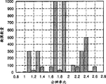
图11画出了输入图像数据的新分辨率与显示板的分辨率之间的比值是1.4∶1的时候,第二个虚拟屏幕VDS上的像素区域,相对于第一个虚拟屏幕VSS上的单元像素区域,子像素区域在不同的水平和垂直位置上。在图11中,实线给出的区域都是第一个虚拟屏幕VSS上的像素区域,虚线给出的区域都是第二个虚拟屏幕VDS上的子像素。在第二个虚拟屏幕VDS上,中心有圆形图案的区域是红色子像素区域,中心有方形图案的区域是绿色子像素区域,中心有钻石图案的区域是蓝色子像素区域。参考图11,子像素区域不同水平位置的数量是15,不同垂直位置的数量是10。换句话说,在图4所示的步骤S4中必须使用150个掩模。因此,在步骤S6中,面积比乘以变换过的图像数据的次数会相对地增加,从而降低显示速度,增加必不可少的存储器容量。Figure 11 shows the pixel area on the second virtual screen V DS relative to the first virtual screen V SS when the ratio between the new resolution of the input image data and the resolution of the display panel is 1.4:1 On the unit pixel area, the sub-pixel area is in different horizontal and vertical positions. In FIG. 11 , the areas indicated by solid lines are all pixel areas on the first virtual screen V SS , and the areas indicated by dotted lines are all sub-pixels on the second virtual screen V DS . On the second virtual screen VDS , the area with a circular pattern in the center is a red sub-pixel area, the area with a square pattern in the center is a green sub-pixel area, and the area with a diamond pattern in the center is a blue sub-pixel area. Referring to FIG. 11 , the number of different horizontal positions of the sub-pixel area is 15, and the number of different vertical positions is 10. In other words, 150 masks must be used in step S4 shown in FIG. 4 . Therefore, in step S6, the number of times the area ratio is multiplied by the transformed image data is relatively increased, thereby reducing the display speed and increasing the necessary memory capacity.
图12画出了输入图像数据新分辨率与显示板分辨率之比为1.5∶1的情况下,第二个虚拟屏幕VDS上的子像素区域,相对于第一个虚拟屏幕VSS上的单元像素区域,它们位于不同的水平和垂直位置上。在图12中,实线划出的区域是第一个虚拟屏幕VSS上的像素区域。在第二个虚拟屏幕VDS上,中心有圆圈的区域是红色子像素区域,中心有方形的区域是绿色子像素区域,中心有钻石图案的区域是蓝色子像素区域。参考图12,子像素区域不同水平位置的数量为0,不同垂直位置的数量是4。换句话说,在图4所示的步骤S4中只用了4个掩模。因此,在步骤S6中,面积比与变换过的图像数据相乘的次数减少了,从而提高了显示速度。例如,在图4所示的步骤S5获得了表1所示的面积比表。Figure 12 shows the sub-pixel area on the second virtual screen V DS relative to the sub-pixel area on the first virtual screen V SS when the ratio of the new resolution of the input image data to the resolution of the display panel is 1.5:1 Unit pixel areas, which are located at different horizontal and vertical positions. In FIG. 12 , the area delineated by the solid line is the pixel area on the first virtual screen V SS . On the second virtual screen VDS , the area with a circle in the center is a red sub-pixel area, the area with a square in the center is a green sub-pixel area, and the area with a diamond pattern in the center is a blue sub-pixel area. Referring to FIG. 12 , the number of different horizontal positions of the sub-pixel area is 0, and the number of different vertical positions is four. In other words, only 4 masks are used in step S4 shown in FIG. 4 . Therefore, in step S6, the number of times the area ratio is multiplied by the converted image data is reduced, thereby increasing the display speed. For example, the area ratio table shown in Table 1 is obtained in step S5 shown in FIG. 4 .
表1
在这里,图8B所示的掩模对应于表1中的掩模C。参考图8B和表1中的掩模C,区域ALL具有面积比7,区域ARL具有面积比14,区域ALU具有面积比5,区域ARU具有面积比10。Here, the mask shown in FIG. 8B corresponds to mask C in Table 1. Referring to FIG. 8B and mask C in Table 1, the area A LL has an area ratio of 7, the area A RL has an area ratio of 14, the area A LU has an area ratio of 5, and the area A RU has an area ratio of 10.
因此,从图11和图12可以推断要使用的掩模的数量通过执行图4所示的步骤S1而最小。Therefore, it can be deduced from FIGS. 11 and 12 that the number of masks to be used is minimized by performing step S1 shown in FIG. 4 .
图13A说明显示板的子像素区域具有德尔塔结构的时候,相对于水平分辨率比,不同水平位置的数量。在这里,德尔塔结构是图3所示第二个虚拟屏幕VDS中画出的子像素阵列结构。参考图13A,最好是为输入图像数据设置一个新的水平分辨率,从而使新的水平分辨率与显示板水平分辨率之间的比值为1∶1、1.5∶1或者2∶1。Figure 13A illustrates the number of different horizontal positions with respect to the horizontal resolution ratio when the sub-pixel area of the display panel has a delta structure. Here, the delta structure is the sub-pixel array structure drawn in the second virtual screen V DS shown in FIG. 3 . Referring to FIG. 13A, it is preferable to set a new horizontal resolution for input image data such that the ratio between the new horizontal resolution and the horizontal resolution of the display panel is 1:1, 1.5:1 or 2:1.
图13B给出了显示板的子像素区域具有德尔塔结构的时候,不同垂直位置的数量相对于垂直分辨率比之间的关系。参考图13B,最好是为输入图像数据设置一个新的垂直分辨率,从而使新的垂直分辨率与显示板垂直分辨率的比等于1∶1、1.2∶1、1.5∶1、1.6∶1或者2∶1。FIG. 13B shows the relationship between the number of different vertical positions and the vertical resolution ratio when the sub-pixel area of the display panel has a delta structure. Referring to FIG. 13B, it is preferable to set a new vertical resolution for the input image data such that the ratio of the new vertical resolution to the vertical resolution of the display panel is equal to 1:1, 1.2:1, 1.5:1, 1.6:1 Or 2:1.
图14说明显示板的子像素区域具有条形结构的时候,掩模的数量与分辨率比之间的关系。在这种情况下,分辨率比表示垂直分辨率比和水平分辨率比,它们是相同的。对于条形结构,红色子像素区域位于第一条线上,绿色子像素区域位于第二条线上,蓝色子像素区域位于第三条线上。图14中的详细数据在表2A~2C中给出。FIG. 14 illustrates the relationship between the number of masks and the resolution ratio when the sub-pixel region of the display panel has a stripe structure. In this case, the resolution ratio means a vertical resolution ratio and a horizontal resolution ratio, which are the same. For the strip structure, the red sub-pixel area is located on the first line, the green sub-pixel area is located on the second line, and the blue sub-pixel area is located on the third line. Detailed data in Figure 14 are given in Tables 2A-2C.
表2A
表2B
表2C
显示板子像素区域的德尔塔类型结构比条形结构更好,因为条形结构中,位于特定子像素上面和下面的子像素具有相同的颜色,从而在划分子像素的过程中,相对于德尔塔结构,垂直方向上位于特定子像素上,有一个掩模重叠的第一个虚图像单元对子像素没有那么大的影响。The delta-type structure of the sub-pixel area of the display panel is better than the bar-shaped structure, because in the bar-shaped structure, the sub-pixels located above and below a specific sub-pixel have the same color, so that in the process of dividing the sub-pixels, relative to the delta-type structure structure, vertically located on a specific sub-pixel, the first virtual image unit with a mask overlap does not have that much effect on the sub-pixel.
图15说明显示板的子像素区域具有德尔塔结构的时候,掩模的数量相对于分辨率比的关系。在这种情况下,分辨率比表示垂直分辨率比和水平分辨率比,它们是相同的。图15中的详细数据在表3A~3CFIG. 15 illustrates the relationship between the number of masks and the resolution ratio when the sub-pixel area of the display panel has a delta structure. In this case, the resolution ratio means a vertical resolution ratio and a horizontal resolution ratio, which are the same. The detailed data in Figure 15 are in Tables 3A-3C
表3A
表3B
表3C
与此同时,当第二个虚拟屏幕叠加在第一个虚拟屏幕上的时候,最好是第一个虚拟屏幕上每个像素区域的中心线不是第二个虚拟屏幕上每个子像素的中心线。下面解释原因。At the same time, when the second virtual screen is superimposed on the first virtual screen, it is better that the center line of each pixel area on the first virtual screen is not the center line of each sub-pixel on the second virtual screen . The reason is explained below.
图16A说明第一个虚拟屏幕上像素区域的中心线是第二个虚拟屏幕上子像素区域中心线这种情形。图16B说明第一个虚拟屏幕上像素区域的中心线不是第二个虚拟屏幕上子像素区域中心线这种情形。在图16A和16B中,符号VP11~VP23表示第一个虚拟屏幕上的一些像素区域。符号CR22表示第二个虚拟屏幕上的红色子像素区域。符号CG22表示第二个虚拟屏幕上的绿色子像素区域,CB22表示第二个虚拟屏幕上的蓝色子像素区域。符号MR22表示红色子像素区域CR22的掩模,符号MG22表示绿色子像素区域CG22的掩模,符号MB22表示蓝色子像素区域CB22的掩模。FIG. 16A illustrates the situation that the centerline of the pixel area on the first virtual screen is the centerline of the sub-pixel area on the second virtual screen. FIG. 16B illustrates the situation that the centerline of the pixel area on the first virtual screen is not the centerline of the sub-pixel area on the second virtual screen. In FIGS. 16A and 16B, symbols VP 11 to VP 23 denote some pixel areas on the first virtual screen. Symbol CR 22 represents the red sub-pixel area on the second virtual screen. Symbol CG 22 denotes a green sub-pixel area on the second virtual screen, and CB 22 denotes a blue sub-pixel area on the second virtual screen. Symbol MR 22 denotes the mask of the red sub-pixel region CR 22 , symbol MG 22 denotes the mask of the green sub-pixel region CG 22 , and symbol MB 22 denotes the mask of the blue sub-pixel region CB 22 .
参考图16A,第一个虚拟屏幕上一个像素区域的中心线是第二个虚拟屏幕上绿色子像素区域CG22的垂直中心线。在这种状态下执行步骤S4、S5、S6的时候,可能会出现颜色偏差现象,其中的绿色看起来更加显眼。当绿色更加显眼的时候,观看者很容易注意到这一颜色偏差现象。Referring to FIG. 16A, the center line of a pixel area on the first virtual screen is the vertical center line of the green sub-pixel area CG22 on the second virtual screen. When performing steps S4, S5, and S6 in this state, color deviation may occur, and the green color is more conspicuous. When the green is more prominent, the viewer can easily notice this color shift phenomenon.
但是,如图16B所示,当第一个虚拟屏幕上像素区域的垂直中心线是第二个虚拟屏幕上绿色和蓝色子像素区域CG22和CB22之间的中心线的时候,绿色和蓝色的混合色,也就是一种青色,会更加醒目。当一种青色更加醒目的时候,观看者不会很容易地发现颜色偏差现象。However, as shown in FIG. 16B, when the vertical centerline of the pixel region on the first virtual screen is the centerline between the green and blue sub-pixel regions CG 22 and CB 22 on the second virtual screen, the green and blue sub-pixel regions CG 22 and CB 22 A blue blend, which is a teal, will stand out even more. When a cyan color is more striking, the viewer will not easily find the color shift phenomenon.
同样,当第一个虚拟屏幕上像素区域的垂直中心线是第二个虚拟屏幕上红色和蓝色子像素区域CR22和CB22之间的中心线的时候,红色和蓝色的混合色,也就是一种深红色,会更加醒目。一种深红色更加醒目的时候,观看者不会很容易地注意到这一颜色偏差现象。Similarly, when the vertical center line of the pixel area on the first virtual screen is the center line between the red and blue sub-pixel areas CR 22 and CB 22 on the second virtual screen, the mixed color of red and blue, That is, a deep red, which will be more eye-catching. When a deep red is more striking, the viewer will not easily notice this color shift phenomenon.
与此同时,参考图8A和12,当输入图像数据的新分辨率与显示板分辨率的比值为1.5∶1的时候,第一个虚拟屏幕VSS上像素区域的垂直中心线不是第二个虚拟屏幕VDS上子像素区域的垂直中心线。Meanwhile, referring to Figs. 8A and 12, when the ratio of the new resolution of the input image data to the resolution of the display panel is 1.5:1, the vertical center line of the pixel area on the first virtual screen V SS is not the second The vertical centerline of the sub-pixel area on the virtual screen V DS .
本发明可以应用于所有类型的显示装置,包括例如等离子体显示板(PDP)、液晶显示(LCD)板和铁电液晶(FLC)板。The present invention can be applied to all types of display devices including, for example, plasma display panels (PDP), liquid crystal display (LCD) panels, and ferroelectric liquid crystal (FLC) panels.
能够用于利用本发明的装置可以包括例如电视、计算机和其它多媒体或者电信装置。例如,如图17所示,按照本发明处理图像数据产生输出图像数据,驱动显示板的装置可以包括与显示控制器102和显示存储器104连接的等离子体显示板100这样的显示板。处理器或者控制106处理图像存储器108中储存的图像数据,并且将处理过的图像数据传送给显示存储器104,在那里,传输过去的数据由显示控制器102进行管理,在显示板100上显示出来。Devices that can be used to utilize the present invention may include, for example, televisions, computers, and other multimedia or telecommunications devices. For example, as shown in FIG. 17 , the means for driving a display panel may include a display panel such as a
图18画出了按照本发明处理图像数据,产生输出图像数据,驱动显示板的另一种装置。显示板100由控制器112利用存储器或者计算机能够读的媒介114(例如非易失性只读存储器,随机存取存储器,软盘,光盘,数字多功能盘,硬盘驱动器,快闪只读存储器,其它光盘和磁介质等等),控制。Fig. 18 illustrates another apparatus for processing image data, generating output image data, and driving a display panel according to the present invention.
参考图19,采用本发明的另一个装置实例是与计算机单元200连接的一个显示器单元150,计算机单元200与一台远程计算机300连接。等离子体显示板这样的显示板100由显示驱动单元120驱动,并且通过显示单元150的接口130和计算机单元200的接口210与计算机200连接。通过系统总线,显示接口210与系统存储器220(只读存储器,随机存取存储器)和存储媒介240(例如非易失性只读存储器,随机存取存储器,软盘,光盘,数字多功能盘,硬盘驱动器,快闪只读存储器,其它光盘和磁介质等等)这样的计算机能够读的媒介连接。系统总线还将计算机处理器230与计算机能够读的媒介连接,并且包括通过输入装置262和其它输入和输出装置260的输入。计算机单元200还可以通过网络接口250和因特网这样的网络400与远程计算机300连接。Referring to FIG. 19, another example of an apparatus employing the present invention is a
如上所述,本发明中处理图像数据的方法具有以下特征。As described above, the method of processing image data in the present invention has the following features.
首先,可以为输入图像数据设置一个新分辨率,以便使具有相同面积比结构的掩模的数量最多。因此,要使用的掩模的数量最少,从而使面积比乘以转换过的图像数据的次数最少,提高显示速度,降低必需的存储器容量。First, a new resolution can be set for the input image data in order to maximize the number of masks with structures of the same area ratio. Therefore, the number of masks to be used is minimized, thereby minimizing the number of times the area ratio is multiplied by the converted image data, increasing the display speed, and reducing the necessary memory capacity.
其次,显示板的每个子像素都与第一个虚拟屏幕上与它相邻像素的数据相关联,因而能够基本上解决显示板子像素阵列结构在再现图像的时候带来的问题。Secondly, each sub-pixel of the display panel is associated with the data of its adjacent pixels on the first virtual screen, thus basically solving the problems caused by the sub-pixel array structure of the display panel when reproducing images.
另外,还能够校正数据处理过程中可能出现的颜色偏差。In addition, color deviations that may occur during data processing can be corrected.
本发明不限于上述实施方案,对于本领域中的技术人员而言,显然能够对它进行各种改变,而不会偏离本发明的实质。The present invention is not limited to the above-mentioned embodiments, and it is obvious to those skilled in the art that various changes can be made thereto without departing from the essence of the present invention.
Claims (57)
Applications Claiming Priority (2)
| Application Number | Priority Date | Filing Date | Title |
|---|---|---|---|
| KR10-2002-0067967A KR100436715B1 (en) | 2002-11-04 | 2002-11-04 | Method of fast processing image data for improving reproducibility of image |
| KR67967/2002 | 2002-11-04 |
Publications (1)
| Publication Number | Publication Date |
|---|---|
| CN1499477A true CN1499477A (en) | 2004-05-26 |
Family
ID=32089789
Family Applications (1)
| Application Number | Title | Priority Date | Filing Date |
|---|---|---|---|
| CNA031483372A Pending CN1499477A (en) | 2002-11-04 | 2003-06-30 | A Method of Quickly Processing Image Data and Improving Image Definition |
Country Status (5)
| Country | Link |
|---|---|
| US (1) | US6958761B2 (en) |
| EP (1) | EP1416468A3 (en) |
| JP (1) | JP4194432B2 (en) |
| KR (1) | KR100436715B1 (en) |
| CN (1) | CN1499477A (en) |
Cited By (12)
| Publication number | Priority date | Publication date | Assignee | Title |
|---|---|---|---|---|
| CN100422924C (en) * | 2005-04-30 | 2008-10-01 | 广东威创视讯科技股份有限公司 | Computer structure for displaying single whole desktop by multiple output channels |
| CN100513174C (en) * | 2004-07-06 | 2009-07-15 | 佳能株式会社 | Data processing method, data processing apparatus, mask generation method, and mask pattern |
| CN101686322B (en) * | 2008-09-24 | 2012-02-22 | 三星Techwin株式会社 | Digital camera device and tracking method |
| CN102982536A (en) * | 2012-11-05 | 2013-03-20 | 华为技术有限公司 | Image processing method and device |
| CN103903549A (en) * | 2014-03-25 | 2014-07-02 | 京东方科技集团股份有限公司 | Display method |
| CN103915044A (en) * | 2014-03-25 | 2014-07-09 | 京东方科技集团股份有限公司 | Display method |
| CN103927946A (en) * | 2014-03-25 | 2014-07-16 | 京东方科技集团股份有限公司 | Display method |
| CN104658503A (en) * | 2015-03-09 | 2015-05-27 | 深圳市华星光电技术有限公司 | Driving method and driving device of liquid crystal display |
| WO2016011728A1 (en) * | 2014-07-23 | 2016-01-28 | 京东方科技集团股份有限公司 | Image display method and display device |
| CN107941256A (en) * | 2017-11-20 | 2018-04-20 | 中国电子科技集团公司第四十研究所 | A kind of numerical value personalized indication method of high precision measuring instrument |
| CN110428354A (en) * | 2019-06-25 | 2019-11-08 | 福建华佳彩有限公司 | The panel method of sampling, storage medium and computer |
| CN112185304A (en) * | 2020-09-28 | 2021-01-05 | 南京芯视元电子有限公司 | Video display system and method for reducing storage capacity and improving display resolution |
Families Citing this family (9)
| Publication number | Priority date | Publication date | Assignee | Title |
|---|---|---|---|---|
| CN100452145C (en) * | 2004-07-30 | 2009-01-14 | 株式会社日立制作所 | Image display device and image display method |
| KR101208724B1 (en) * | 2005-01-03 | 2012-12-06 | 삼성디스플레이 주식회사 | Array substrate and display panel having the same |
| JP4777675B2 (en) * | 2005-03-17 | 2011-09-21 | 株式会社リコー | Image processing apparatus, image display apparatus, image processing method, program for causing computer to execute the method, and recording medium |
| US8049685B2 (en) * | 2006-11-09 | 2011-11-01 | Global Oled Technology Llc | Passive matrix thin-film electro-luminescent display |
| CN104680994B (en) * | 2015-03-09 | 2017-09-15 | 深圳市华星光电技术有限公司 | The driving method and drive device of a kind of liquid crystal display |
| CN104680966B (en) * | 2015-03-19 | 2017-11-14 | 京东方科技集团股份有限公司 | The driving method and its drive device of a kind of display device |
| CN106157876B (en) * | 2015-03-27 | 2019-04-23 | 上海和辉光电有限公司 | The display methods and display of display image |
| KR102389196B1 (en) * | 2015-10-05 | 2022-04-22 | 엘지디스플레이 주식회사 | Display device and image rendering method thereof |
| CN117894269B (en) * | 2024-03-14 | 2024-07-02 | 集创北方(珠海)科技有限公司 | Data processing method, processing device and chip |
Family Cites Families (41)
| Publication number | Priority date | Publication date | Assignee | Title |
|---|---|---|---|---|
| US632896A (en) * | 1898-09-14 | 1899-09-12 | Whitfield Company | Combined engine and dynamo. |
| JPS57138685A (en) * | 1981-02-23 | 1982-08-27 | Hitachi Ltd | Graphic conversion for graphic indicator |
| JPS60120398A (en) * | 1983-12-02 | 1985-06-27 | シチズン時計株式会社 | Matrix type color display unit |
| US5341153A (en) * | 1988-06-13 | 1994-08-23 | International Business Machines Corporation | Method of and apparatus for displaying a multicolor image |
| US5682180A (en) * | 1990-06-08 | 1997-10-28 | General Motors Corporation | Multi-color electronic display utilizing opponent colors |
| US5426723A (en) * | 1992-03-09 | 1995-06-20 | Spacelabs Medical, Inc. | System and method for scaling graphic images |
| JP2797883B2 (en) * | 1993-03-18 | 1998-09-17 | 株式会社日立製作所 | Multicolor light emitting device and its substrate |
| KR100259783B1 (en) * | 1994-03-11 | 2000-06-15 | 미다라이 후지오 | Display pixel balancing for multiple color individual level displays |
| US5796378A (en) * | 1994-03-29 | 1998-08-18 | Casio Computer Co., Ltd. | Birifringence control type liquid crystal display device and apparatus and method of driving the same |
| TW295652B (en) * | 1994-10-24 | 1997-01-11 | Handotai Energy Kenkyusho Kk | |
| JP3309593B2 (en) * | 1994-10-28 | 2002-07-29 | 松下電器産業株式会社 | Plasma display |
| US5959598A (en) * | 1995-07-20 | 1999-09-28 | The Regents Of The University Of Colorado | Pixel buffer circuits for implementing improved methods of displaying grey-scale or color images |
| US6031626A (en) * | 1996-08-15 | 2000-02-29 | Seiko Epson Corporation | Color stochastic screening with optimal color dot placement |
| US5963715A (en) * | 1996-08-15 | 1999-10-05 | Seiko Epson Corporation | Color stochastic screening with optimal color dot placement for display devices having arbitrary aspect ratios |
| US6078303A (en) * | 1996-12-19 | 2000-06-20 | Colorado Microdisplay, Inc. | Display system having electrode modulation to alter a state of an electro-optic layer |
| US5920298A (en) * | 1996-12-19 | 1999-07-06 | Colorado Microdisplay, Inc. | Display system having common electrode modulation |
| US6046716A (en) * | 1996-12-19 | 2000-04-04 | Colorado Microdisplay, Inc. | Display system having electrode modulation to alter a state of an electro-optic layer |
| US6020868A (en) * | 1997-01-09 | 2000-02-01 | Rainbow Displays, Inc. | Color-matching data architectures for tiled, flat-panel displays |
| JPH10254370A (en) * | 1997-03-10 | 1998-09-25 | Canon Inc | Display panel and projection display device using the same |
| US5913591A (en) * | 1998-01-20 | 1999-06-22 | University Of Washington | Augmented imaging using a silhouette to improve contrast |
| US6100861A (en) * | 1998-02-17 | 2000-08-08 | Rainbow Displays, Inc. | Tiled flat panel display with improved color gamut |
| US6281875B1 (en) * | 1998-04-29 | 2001-08-28 | Canon Kabushiki Kaisha | Gradient-based pixel interpolation |
| US6236390B1 (en) * | 1998-10-07 | 2001-05-22 | Microsoft Corporation | Methods and apparatus for positioning displayed characters |
| CN1175391C (en) * | 1998-10-07 | 2004-11-10 | 微软公司 | A Method for Mapping Samples of Foreground/Background Color Image Data to Pixel Subcomponents |
| US6188385B1 (en) * | 1998-10-07 | 2001-02-13 | Microsoft Corporation | Method and apparatus for displaying images such as text |
| US6278434B1 (en) * | 1998-10-07 | 2001-08-21 | Microsoft Corporation | Non-square scaling of image data to be mapped to pixel sub-components |
| US6307566B1 (en) * | 1998-10-07 | 2001-10-23 | Microsoft Corporation | Methods and apparatus for performing image rendering and rasterization operations |
| US6356278B1 (en) * | 1998-10-07 | 2002-03-12 | Microsoft Corporation | Methods and systems for asymmeteric supersampling rasterization of image data |
| US6393145B2 (en) * | 1999-01-12 | 2002-05-21 | Microsoft Corporation | Methods apparatus and data structures for enhancing the resolution of images to be rendered on patterned display devices |
| US6342890B1 (en) * | 1999-03-19 | 2002-01-29 | Microsoft Corporation | Methods, apparatus, and data structures for accessing sub-pixel data having left side bearing information |
| US6342896B1 (en) | 1999-03-19 | 2002-01-29 | Microsoft Corporation | Methods and apparatus for efficiently implementing and modifying foreground and background color selections |
| US6339426B1 (en) * | 1999-04-29 | 2002-01-15 | Microsoft Corporation | Methods, apparatus and data structures for overscaling or oversampling character feature information in a system for rendering text on horizontally striped displays |
| US6738526B1 (en) * | 1999-07-30 | 2004-05-18 | Microsoft Corporation | Method and apparatus for filtering and caching data representing images |
| US6226017B1 (en) * | 1999-07-30 | 2001-05-01 | Microsoft Corporation | Methods and apparatus for improving read/modify/write operations |
| US6282327B1 (en) * | 1999-07-30 | 2001-08-28 | Microsoft Corporation | Maintaining advance widths of existing characters that have been resolution enhanced |
| US6384839B1 (en) * | 1999-09-21 | 2002-05-07 | Agfa Monotype Corporation | Method and apparatus for rendering sub-pixel anti-aliased graphics on stripe topology color displays |
| KR100408213B1 (en) * | 2000-06-26 | 2003-12-01 | 황기웅 | an AC plasma display panel having delta color pixels of closed shape subpixels |
| KR20020008040A (en) * | 2000-07-18 | 2002-01-29 | 마츠시타 덴끼 산교 가부시키가이샤 | Display apparatus, display method, and recording medium which the display control program is recorded |
| CN1179312C (en) * | 2000-07-19 | 2004-12-08 | 松下电器产业株式会社 | display method |
| TW540022B (en) * | 2001-03-27 | 2003-07-01 | Koninkl Philips Electronics Nv | Display device and method of displaying an image |
| KR100446631B1 (en) * | 2002-08-24 | 2004-09-04 | 삼성전자주식회사 | Method and apparatus for rendering color image on delta structured displays |
-
2002
- 2002-11-04 KR KR10-2002-0067967A patent/KR100436715B1/en not_active Expired - Fee Related
-
2003
- 2003-04-03 US US10/405,909 patent/US6958761B2/en not_active Expired - Fee Related
- 2003-06-27 EP EP03254131A patent/EP1416468A3/en not_active Ceased
- 2003-06-30 JP JP2003188436A patent/JP4194432B2/en not_active Expired - Fee Related
- 2003-06-30 CN CNA031483372A patent/CN1499477A/en active Pending
Cited By (21)
| Publication number | Priority date | Publication date | Assignee | Title |
|---|---|---|---|---|
| CN100513174C (en) * | 2004-07-06 | 2009-07-15 | 佳能株式会社 | Data processing method, data processing apparatus, mask generation method, and mask pattern |
| CN100422924C (en) * | 2005-04-30 | 2008-10-01 | 广东威创视讯科技股份有限公司 | Computer structure for displaying single whole desktop by multiple output channels |
| CN101686322B (en) * | 2008-09-24 | 2012-02-22 | 三星Techwin株式会社 | Digital camera device and tracking method |
| CN102982536B (en) * | 2012-11-05 | 2015-07-22 | 华为技术有限公司 | Image processing method and device |
| CN102982536A (en) * | 2012-11-05 | 2013-03-20 | 华为技术有限公司 | Image processing method and device |
| CN103915044B (en) * | 2014-03-25 | 2016-03-30 | 京东方科技集团股份有限公司 | Display packing |
| US9875682B2 (en) | 2014-03-25 | 2018-01-23 | Boe Technology Group Co., Ltd. | Display method and display panel |
| US10325539B2 (en) | 2014-03-25 | 2019-06-18 | Boe Technology Group Co., Ltd. | Display method, display panel and display device |
| CN103915044A (en) * | 2014-03-25 | 2014-07-09 | 京东方科技集团股份有限公司 | Display method |
| CN103927946A (en) * | 2014-03-25 | 2014-07-16 | 京东方科技集团股份有限公司 | Display method |
| CN103903549A (en) * | 2014-03-25 | 2014-07-02 | 京东方科技集团股份有限公司 | Display method |
| CN103927946B (en) * | 2014-03-25 | 2016-06-08 | 京东方科技集团股份有限公司 | Display packing |
| CN103903549B (en) * | 2014-03-25 | 2016-08-17 | 京东方科技集团股份有限公司 | Display packing |
| WO2016011728A1 (en) * | 2014-07-23 | 2016-01-28 | 京东方科技集团股份有限公司 | Image display method and display device |
| US9613564B2 (en) | 2014-07-23 | 2017-04-04 | Boe Technology Group Co., Ltd. | Image displaying method and image display apparatus |
| CN104658503A (en) * | 2015-03-09 | 2015-05-27 | 深圳市华星光电技术有限公司 | Driving method and driving device of liquid crystal display |
| CN107941256A (en) * | 2017-11-20 | 2018-04-20 | 中国电子科技集团公司第四十研究所 | A kind of numerical value personalized indication method of high precision measuring instrument |
| CN107941256B (en) * | 2017-11-20 | 2020-03-06 | 中国电子科技集团公司第四十一研究所 | A Numerical Personalized Display Method of High Precision Measuring Instrument |
| CN110428354A (en) * | 2019-06-25 | 2019-11-08 | 福建华佳彩有限公司 | The panel method of sampling, storage medium and computer |
| CN110428354B (en) * | 2019-06-25 | 2023-04-07 | 福建华佳彩有限公司 | Panel sampling method, storage medium and computer |
| CN112185304A (en) * | 2020-09-28 | 2021-01-05 | 南京芯视元电子有限公司 | Video display system and method for reducing storage capacity and improving display resolution |
Also Published As
| Publication number | Publication date |
|---|---|
| US6958761B2 (en) | 2005-10-25 |
| EP1416468A3 (en) | 2005-07-27 |
| US20040085333A1 (en) | 2004-05-06 |
| JP2004157514A (en) | 2004-06-03 |
| JP4194432B2 (en) | 2008-12-10 |
| KR20040039783A (en) | 2004-05-12 |
| EP1416468A2 (en) | 2004-05-06 |
| KR100436715B1 (en) | 2004-06-22 |
Similar Documents
| Publication | Publication Date | Title |
|---|---|---|
| CN1499477A (en) | A Method of Quickly Processing Image Data and Improving Image Definition | |
| CN1266648C (en) | Method and device for reproducing image signal | |
| CN103792723B (en) | Display base plate, manufacturing method thereof, driving method and display device | |
| CN1530909A (en) | display device | |
| CN1799080A (en) | Liquid crystal display backplane layouts and addressing for non-standard subpixel arrangements | |
| CN1639765A (en) | Subpixel Arrangement and Subpixel Rendering Setup for Color Flat Panel Displays | |
| CN1678950A (en) | Active matrix drive display and image display method using same | |
| CN1475816A (en) | Color filter substrate and display device | |
| KR102239895B1 (en) | Method and data converter for upscailing of input display data | |
| CN103207489A (en) | Pixel structure, driving method thereof and display device | |
| CN1549240A (en) | pixel driving module of display | |
| CN108428435A (en) | A kind of verification display methods that Delta types arrangement sub-pixel renders | |
| CN107633809A (en) | Eliminate method, display screen and the display device of more IC drivings display screen concealed wires | |
| WO2010016319A1 (en) | Image processing device, display device, image processing method, program, and recording medium | |
| CN1161738C (en) | Liquid crystal display device and driving method thereof | |
| CN101292279B (en) | Improved memory structure for image processing | |
| CN1776799A (en) | Driving method of high frame rate display system | |
| US20050212741A1 (en) | Transistor backplanes for liquid crystal displays comprising different sized subpixels | |
| CN104062825B (en) | Array substrate, display panel and display device | |
| CN103488017A (en) | Active array substrate, driving method thereof and liquid crystal display panel using active array substrate | |
| JP2020507133A (en) | Driving method of liquid crystal display panel | |
| CN104966484A (en) | Display panel and driving method thereof | |
| JP2005316169A (en) | Color image display apparatus | |
| CN101266745A (en) | Display device and driving method thereof | |
| TWI594230B (en) | Display apparatus and operating method thereof |
Legal Events
| Date | Code | Title | Description |
|---|---|---|---|
| C06 | Publication | ||
| PB01 | Publication | ||
| C10 | Entry into substantive examination | ||
| SE01 | Entry into force of request for substantive examination | ||
| AD01 | Patent right deemed abandoned |
Effective date of abandoning: 20040526 |
|
| C20 | Patent right or utility model deemed to be abandoned or is abandoned |