CN1499472A - Gamma correcting device for liquid crystal display and LCD for device - Google Patents
Gamma correcting device for liquid crystal display and LCD for device Download PDFInfo
- Publication number
- CN1499472A CN1499472A CNA021503540A CN02150354A CN1499472A CN 1499472 A CN1499472 A CN 1499472A CN A021503540 A CNA021503540 A CN A021503540A CN 02150354 A CN02150354 A CN 02150354A CN 1499472 A CN1499472 A CN 1499472A
- Authority
- CN
- China
- Prior art keywords
- gray scale
- voltage output
- output circuit
- scale voltage
- indivedual
- Prior art date
- Legal status (The legal status is an assumption and is not a legal conclusion. Google has not performed a legal analysis and makes no representation as to the accuracy of the status listed.)
- Granted
Links
Images


Landscapes
- Liquid Crystal Display Device Control (AREA)
- Control Of Indicators Other Than Cathode Ray Tubes (AREA)
Abstract
Gamma correcting device includes gray scale voltage output circuit and gamma correcting circuit. The gray scale voltage output circuit includes common gray scale voltage output circuit and multiple individual gray scale voltage output circuits. Each individual gray scale voltage output circuit outputs specific gray scale voltage, which is corresponding to one of colors displayed on pixels of liquid crystal faceplate. Based on displayed color of pixel signal, the gamma correcting circuit selects common gray scale voltage and corresponding individual gray scale voltage to output pixel voltages relevant to pixel signal.
Description
Technical field
The present invention relates to a kind of digital analogue signal conversion equipment and method, and be particularly related to a kind of gamma (gamma) means for correcting that is used for LCD, method and with the LCD of this device.
Background technology
(Liquid Crystal Display LCD) has the advantage of thin, the in light weight and low electromagnetic of volume, is widely used gradually in recent years because LCD.
Have a plurality of pixels (pixel) of arranging on the LCD screen with matrix form.Each pixel is made up of the liquid crystal layer between upper plate, lower plate and upper plate and the lower plate.The arrangement mode of the liquid crystal molecule of liquid crystal layer can change along with the voltage difference of the voltage that puts on upper plate and lower plate respectively, and then influences the brightness of pixel.So, can control the brightness of each pixel on the LCD screen by controlling the voltage swing that put on upper plate and lower plate respectively.Wherein, the difference of upper plate voltage and lower plate voltage is called gray scale voltage.
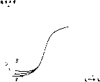
Please refer to Fig. 1, it is depicted as the pixel voltage of input pixel and the gamma curve graph of a relation of pixel intensity.Pixel voltage and brightness are not linear, but the relation of gamma curve as shown in Figure 1.In addition, the brightness of pixel is only relevant with the size of pixel voltage, and irrelevant with the polarity of pixel voltage.Therefore, gamma curve is by being the center with the ordinate, and symmetrical positive polarity gamma curve 102 and negative polarity gamma curve 104 are formed.If a certain pixel is imported two respectively size is identical but pixel voltage that polarity is different, then this pixel can have identical brightness.In the time will making a certain pixel show same brightness for a long time, can protect liquid crystal molecule by alternatively changing the polarity of pixel voltage.
General picture element signal is the digital signal of binary bit form.Because pixel voltage and pixel intensity are non-linear gamma curve relation, therefore, LCD needs special circuit arrangement, concern in order to the foundation gamma curve, convert the picture element signal of digital format to output corresponding pixel voltage output, make picture element signal and pixel intensity be the linear ratio relation.Action mentioned above is called as gamma correction (gamma correction), in order to improve the image display quality of LCD screen.
Please refer to Fig. 2, it illustrated is the synoptic diagram of gamma correction principle.When carrying out gamma correction, choose a plurality of picture element signals at first earlier as the reference picture element signal.In Fig. 2, with picture element signal D0, D1, D2, D3 and D4 as the reference picture element signal.According to gamma curve, each reference pixel signal can be distinguished a corresponding positive polarity reference voltage and a negative polarity reference voltage.With reference pixel signal D0 is example, and it is a corresponding positive polarity reference voltage V0 and a negative polarity reference voltage V9 respectively.In like manner, 5 reference pixel signal D0, D1, D2, D3 and D4 correspond to respectively 5 positive polarity reference voltage V0, V1, V2, V3, with V4 and 5 negative polarity reference voltage V9, V8, V7, V6 and V5, as shown in Figure 2.When carrying out gamma correction, just the corresponding relation with reference pixel signal and reference voltage is as the criterion, and utilizes interpolation method to try to achieve the corresponding respectively pixel voltage of other all picture element signals.Wherein, each picture element signal all can be distinguished a corresponding positive polarity pixel voltage and a negative polarity pixel voltage.
Be noted that selected reference pixel signal number is many more, when carrying out gamma correction, the pairing pixel voltage of each picture element signal is just accurate more.Generally choose 8 reference pixel signals and carry out gamma correction.According to gamma curve, 8 respectively corresponding 8 positive polarity reference voltages of reference pixel signal and 8 negative polarity reference voltages.The gamma correcting device of being responsible for the action of execution gamma correction promptly is as the criterion with these 16 reference voltages, carries out gamma correction.
Please refer to Fig. 3, it illustrated is the synoptic diagram of traditional gray scale voltage output circuit.General picture element signal DATA is eight a binary bit, can represent 256 GTG values (gray level value) altogether.So in gamma correcting device, a gray scale voltage (gray level voltage) output circuit 300 need be set, in order to reference voltage 256 positive polarity gray scale voltages of output and 256 negative polarity gray scale voltages according to input.Wherein, each gray scale voltage is corresponding with a picture element signal DATA respectively.Gray scale voltage output circuit 300 is made up of two resistance string, respectively in order to output cathode gray scale voltage and negative polarity gray scale voltage.Wherein, each resistance string comprises 255 resistance, and label is R0, R1 respectively ... R254, a plurality of input nodes, in order to import corresponding reference voltage signal V0~V4 respectively, V5~V9, and 256 output nodes are in order to the output gray scale voltage.According to the law of partial pressure, via the resistance value of suitably setting each resistance in the resistance string, can be in each output node output gray scale voltage corresponding of two resistance string with one of digital pixel data DATA person.
Please refer to Fig. 4 A~4G, it illustrates the graph of a relation of multi-form gamma curve respectively.In order to make diagram simple, clear, so Fig. 4 A~4G all only illustrates the gamma curve of part, and its respectively the complete gamma curve of correspondence all can push away easily according to the part gamma curve that Fig. 4 A~4G illustrates.In colour liquid crystal display device, picture element signal according to its color in order to show, can be divided into three kinds of red, green, blues, show the pixel intensity of red, green, blue look respectively in order to control.In Fig. 4 A~4G, three curves that indicate R, G, B are represented when the pixel demonstration is red, green and blue the gray scale voltage of pixel and the gamma curve of pixel intensity relation respectively.The gamma curve relation of the gray scale voltage of input pixel and the brightness of pixel, meeting changes to some extent along with the difference of the kenel (conformation) of liquid crystal molecule in the pixel.The form of the gamma curve that it is possible is shown in Fig. 4 A~4G.In Fig. 4 A, for the pixel that shows different colours, the pixel voltage of input pixel is big more, and the difference of pixel intensity can be big more.The pixel voltage that Fig. 4 B then represents to import pixel is more little, the pixel that Show Color is different, and the difference of its brightness can be big more.Fig. 4 C then is the situation in conjunction with Fig. 4 A and Fig. 4 B, and when the value of pixel voltage of input pixel is big or more little more, for the pixel that shows different colours, the difference of pixel intensity can be big more.Fig. 4 D and Fig. 4 category-A seemingly, its difference is, when the maximal value of input pixel voltage, no matter the Show Color of pixel why, the light transmittance of its liquid crystal molecule is all identical.Fig. 4 E and Fig. 4 category-B seemingly, its difference is, when the minimum value of input pixel voltage, no matter the Show Color of pixel why, the light transmittance of its liquid crystal molecule is all identical.Fig. 4 F and Fig. 4 C are similar, and its difference is, when the maximal value of input pixel voltage and minimum value, no matter the Show Color of pixel why, and the light transmittance of its liquid crystal molecule is all identical.It is big more or more hour, for the pixel of different Show Colors, the difference of pixel intensity can be more little that Fig. 4 G then illustrates pixel voltage when the input pixel, but if during the pixel voltage of the medium value of input, the difference of pixel intensity can become big situation.Wherein, the liquid crystal panel of general TN mode, the gamma curve relation of its pixel is haply shown in Fig. 4 A.And the liquid crystal panel of general VA mode, the gamma curve relation of its pixel is haply shown in Fig. 4 B.
By Fig. 4 A~4G as can be known, though the form of gamma curve can change along with the difference of liquid crystal molecule form in the liquid crystal panel,, its common feature is, gamma curve can be along with the difference of pixel Show Color difference to some extent.
When the tradition gamma correcting device is carried out gamma correction, no matter the Show Color of the pairing pixel of picture element signal why, all decide the corresponding relation of reference pixel signal and reference voltage, and then determine the size of the pairing pixel voltage of each picture element signal according to a fixing gamma curve.So the benefit of the practice is to avoid the gamma-correction circuit complexity too high, and shared volume is too huge in the driving circuit of LCD.But the shortcoming of conventional practice is with different gamma curves, to come picture element signal is carried out gamma correction according to the Show Color of pixel.So, can make picture element signal and pixel intensity can't be the linear ratio relation, and can make pixel can't have maximum brightness in some cases, and then influence the image display quality of liquid crystal panel.
Summary of the invention
In view of this, purpose of the present invention is exactly in that a kind of gamma correcting device and method are provided, and in order to the Show Color at pixel, according to different gamma curves, comes picture element signal is carried out gamma correction.Make picture element signal and pixel intensity be the linear ratio relation, be not subjected to the influence of pixel Show Color, and then improve the image display quality of liquid crystal panel.
According to purpose of the present invention, a kind of gamma correcting device that is used for LCD is proposed, comprise gray scale voltage output circuit and gamma-correction circuit at least.The gray scale voltage output circuit also comprises a common gray scale voltage output circuit, in order to exporting a plurality of common gray scale voltages, and a plurality of indivedual gray scale voltage output circuit.Each indivedual gray scale voltage output circuit couples with common gray scale voltage output circuit respectively, in order to export a plurality of indivedual gray scale voltages.Wherein, on color liquid crystal panel, pixel is available as and shows redness, and is blue and green.Each indivedual gray scale voltage output circuit is corresponding with one of above-mentioned three colors person.And the magnitude of voltage of indivedual gray scale voltages of each indivedual gray scale voltage output circuit output, determined by the pairing color of these indivedual gray scale voltage output circuits.Gamma-correction circuit and gray scale voltage output circuit couple, and in order to according to common gray scale voltage and indivedual gray scale voltage, export and pixel voltages relevant.When picture element signal when showing redness, gamma-correction circuit is according to common gray scale voltage and red gray scale voltage, the pixel voltage that output is corresponding, when picture element signal when showing green, gamma-correction circuit is according to common gray scale voltage and green gray scale voltage, the pixel voltage that output is corresponding, when picture element signal when showing blueness, gamma-correction circuit is according to common gray scale voltage and bluish grey rank voltage, the pixel voltage that output is corresponding.
Description of drawings
For above-mentioned purpose of the present invention, feature and advantage can be become apparent, a preferred embodiment cited below particularly, and cooperate appended graphicly, be described in detail below.
Fig. 1 illustrates the gray scale voltage of pixel and the gamma curve graph of a relation of light transmittance.
Fig. 2 illustrates the synoptic diagram of gamma correction principle.
Fig. 3 illustrates the synoptic diagram of traditional gray scale voltage output circuit.
Fig. 4 A~4G illustrates multi-form gamma curve figure.
Fig. 5 is the circuit diagram of first kind of gray scale voltage output circuit illustrating according to the preferred embodiments of the present invention.
Fig. 6 A~6B illustrates the gamma curve figure that gray scale voltage output circuit shown in Figure 5 is suitable for.
Fig. 7 is the circuit diagram of second kind of gray scale voltage output circuit illustrating according to the preferred embodiments of the present invention.
Fig. 8 illustrates the gamma curve figure that gray scale voltage output circuit shown in Figure 7 is suitable for.
Fig. 9 is the circuit diagram of the third gray scale voltage output circuit of illustrating according to the preferred embodiments of the present invention.
Figure 10 illustrates the gamma curve figure that gray scale voltage output circuit shown in Figure 9 is suitable for.
Figure 11 is the circuit diagram of the 4th kind of gray scale voltage output circuit illustrating according to the preferred embodiments of the present invention.
Figure 12 illustrates the gamma curve graph of a relation that gray scale voltage output circuit shown in Figure 11 is suitable for.
Figure 13 is the circuit diagram of the 5th kind of gray scale voltage output circuit illustrating according to the preferred embodiments of the present invention.
Figure 14 illustrates the gamma curve graph of a relation that gray scale voltage output circuit shown in Figure 13 is suitable for.
Embodiment
Characteristics of the present invention are, the part that differs greatly at the gamma curve of different colours, respectively according to the gamma curve of different colours, the value of the gray scale voltage of decision output gray scale voltage output circuit, and with the corresponding relation of picture element signal.So, when carrying out gamma correction, no matter the color of picture element signal correspondence why, and the value of picture element signal and gray scale voltage all is the linear ratio relation, to improve the image display quality of liquid crystal panel.
Please refer to Fig. 5, it illustrates the circuit diagram of the first kind of gray scale voltage output circuit that proposes according to the preferred embodiments of the present invention.Gray scale voltage output circuit 500 is exported 256 gray scale voltages in order to send out reference pixel voltage according to input.Wherein, each gray scale voltage is corresponding to a picture element signal.Be noted that complete gray scale voltage output circuit need comprise two as the gray scale voltage output circuit 500 that Fig. 5 illustrated, in order to export 256 positive polarity gray scale voltages and 256 negative polarity gray scale voltages respectively.The principle of operation of two gray scale voltage output circuits and method are all closely similar, so after the principle of operation and method of one of them gray scale voltage output circuit 500 of explanation, any those skilled in the art all can push away easily the principle of operation and the method for another gray scale voltage output circuit.
Gray scale voltage output circuit 500 comprises common gray scale voltage output circuit 502 and indivedual gray scale voltage output circuit 504 two parts.And indivedual gray scale voltage output circuits 504 also comprise red gray scale voltage output circuit 506, green gray scale voltage output circuit 508 and bluish grey rank voltage follower circuit 510.Red gray scale voltage output circuit 506, green gray scale voltage output circuit 508 and bluish grey rank voltage follower circuit 510 are coupled to same end points with common gray scale voltage output circuit 502, as shown in Figure 5.
Please refer to Fig. 6 A, it illustrates and is suitable for the gamma curve graph of a relation that gray scale voltage output circuit shown in Figure 5 is carried out gamma correction.In Fig. 6 A, three curves that indicate R, G, B are represented when the pixel demonstration is red, green and blue the gray scale voltage of input pixel and the corresponding relation of pixel intensity respectively.The gamma curve that illustrates by Fig. 6 A as can be known, when pixel voltage hour, for the pixel that shows different colours, the difference of pixel intensity is very little, can ignore.Yet when pixel voltage was big more, the difference of pixel intensity also can increase thereupon.
In the present embodiment, the resistance string of common gray scale voltage output circuit 502 for being in series by 191 resistance.This resistance string has 5 input nodes, in order to input common reference voltage V4, V5, V6, V7 and V8, also has 192 output nodes, respectively in order to export common gray scale voltage VO0~VO191 respectively.According to the law of partial pressure, by the resistance of suitably choosing each resistance, promptly may command is from the value of the gray scale voltage of each output node output.The value of reference voltage V4~V8 is illustrated among Fig. 6 A.In Fig. 6 A, the gamma curve of different colours and the corresponding part of reference voltage V4~V8, difference each other is minimum.Common gray scale voltage output circuit 502 is exported gray scale voltage VO0, VO1 according to reference voltage V4~V8 ... VO191 is corresponding with picture element signal 0~191 (representing with decade) respectively.And for picture element signal 0~191, itself and gray scale voltage VO0, VO1 ... the corresponding relation of VO191, not different along with the Show Color of pixel.
Referring again to Fig. 6 A and Fig. 6 B, in Fig. 6 A, when pixel voltage is big more, the pixel that Show Color is different, the difference of its brightness also can increase thereupon.Fig. 6 B is the enlarged drawing in the zone shown in Fig. 6 A center line.In Fig. 6 B, the gamma curve of different colours difference is to each other showing, and can strengthen along with the increase of gray scale voltage.In order to make the linear ratio relation of picture element signal and pixel intensity, difference to some extent not along with the Show Color of pixel.The present invention is by indivedual gray scale voltage output circuits 504, and according in the gamma curve of red, blue, green three looks, the part that differs greatly (part shown in Fig. 6 B) is exported different gray scale voltages respectively.
In the present embodiment, indivedual gray scale voltage output circuits 504 include red gray scale voltage output circuit 506, green gray scale voltage output circuit 508 and bluish grey rank voltage follower circuit 510 according to the Show Color of pixel on the general color liquid crystal panel.With red gray scale voltage output circuit 506 is example, its resistance string for being in series by 64 resistance.This resistance string has 3 input nodes, in order to input common reference voltage V1R, V2R and V3R, also has 64 output nodes, respectively in order to export red gray scale voltage VO192r~VO255r respectively.Wherein, from the red gray scale voltage VO192r~VO255r of each output node output, its value is according to the gamma curve shown in Fig. 6 B " R " decide.Its mode has two, one, by suitably choosing each resistance (resistance of Rr0~Rr63).Another mode is by the reference voltage that suitably determines the input resistance string (value of V1R~V3R), and each input node position in resistance string.So, according to the law of partial pressure, can determine value from the gray scale voltage of each output node output.Referring again to Fig. 6 B, because reference voltage V1R must be by the input node input topmost of red gray scale voltage output circuit 506, so can only control the value of the gray scale voltage of output by the value of control V1R.But for reference voltage V2R and V3R, can pass through the value of control reference voltage V2R and V3R simultaneously, and on the red gray scale voltage output circuit 506, the position of corresponding input node, decision is from the value of the gray scale voltage of each output node output.By the value of decision, make that the brightness of picture element signal 192~255 and pixel is according to gamma curve from the red gray scale voltage VO192r~VO255r of red gray scale voltage output circuit 506 outputs " R ", be the linear ratio relation.
The circuit of green gray scale voltage output circuit 508 and bluish grey rank voltage follower circuit 510 and operation principles are similar to above-mentioned red gray scale voltage output circuit 506, repeat no more in this.Be noted that green gray scale voltage output circuit 508 and bluish grey rank voltage follower circuit 510 are respectively according to the gamma curve shown in Fig. 6 A~6B " G " reach " B ", decide the value of the gray scale voltage of output.So in green gray scale voltage output circuit 508 and the bluish grey rank voltage follower circuit 510, the resistance of each resistance, the value of each reference voltage, and with the corresponding input node of reference voltage in the position of resistance string, can be not identical with red gray scale voltage output circuit 506.So, make green gray scale voltage VO192g~VO255g from green gray scale voltage output circuit 508 outputs, the brightness of its corresponding picture element signal 192~255 and pixel is according to gamma curve " G " be the linear ratio relation.And from the bluish grey rank voltage VO192b~VO255b of bluish grey rank voltage follower circuit 5 10 output, the brightness of its corresponding picture element signal 192~255 and pixel is according to gamma curve " B " be the linear ratio relation.
Be noted that though in the present embodiment, common gray scale voltage output circuit 502 and indivedual gray scale voltage output circuit 504 are respectively resistance string, the present invention is not as limit.All any can be according to individual other gamma curve, by the reference voltage output of input and the device of the corresponding gray scale voltage of picture element signal, neitherly take off spirit of the present invention.
Described by preamble, the gamma curve relation of the gray scale voltage of input pixel and the brightness of pixel, meeting changes to some extent along with the difference of the kenel of liquid crystal molecule in the pixel.Gray scale voltage output circuit proposed by the invention also can be made suitable change, has been applicable to multi-form gamma curve.Fig. 7 is the circuit diagram of second kind of gray scale voltage output circuit illustrating according to the preferred embodiments of the present invention.Its gray scale voltage VO64~VO255 is exported by common gray scale voltage output circuit, and is corresponding with picture element signal 64~255 respectively.Red gray scale voltage output circuit, green gray scale voltage output circuit and bluish grey rank voltage follower circuit are then respectively according to gamma curve shown in Figure 8 " R ", " G " reach " B ", export red gray scale voltage VO0r~VO63r, green gray scale voltage VO0g~VO63g and bluish grey rank voltage VO0b~VO63b.These three groups of gray scale voltages are all corresponding with picture element signal 0~63.The gray scale voltage output circuit that Fig. 7 illustrated is applicable to the gamma curve relation that Fig. 8 illustrates.The gray scale voltage output circuit that Fig. 9 illustrated, its indivedual gray scale voltage output circuits are divided into two parts.With red gray scale voltage output circuit is example, it is made up of two resistance string, export red gray scale voltage VO255r~VO191r according to reference voltage V1R~V3R respectively, and export red gray scale voltage VO63r~VO1r, as shown in Figure 9 according to reference voltage V6R~V8R.The gray scale voltage output circuit that Fig. 9 illustrated is applicable to the gamma curve relation that Figure 10 illustrates.In like manner, the gray scale voltage output circuit that illustrates of Figure 11 is applicable to the gamma curve relation that Figure 12 illustrates.And the gray scale voltage output circuit that Figure 13 illustrates is applicable to the gamma curve relation that Figure 14 illustrates.Be noted that, though 5th, the gray scale voltage output circuit shown in 7,9,11 and 13 figure and inequality, and also be applicable to multi-form gamma curve, but its common feature is all the part that the gamma curve at different colours differs greatly, respectively according to the gamma curve of different colours, the value of the gray scale voltage of decision output gray scale voltage output circuit, and with the corresponding relation of picture element signal, make the picture element signal of different colours and pixel intensity connect and be the linear ratio relation.So neither disengaging spirit of the present invention.
The gray scale voltage of gray scale voltage output circuit output can input in the gamma-correction circuit.Wherein, gray scale voltage comprises common gray scale voltage and indivedual gray scale voltage, and indivedual gray scale voltages also comprise red gray scale voltage (VOr), green gray scale voltage (VOg) and bluish grey rank voltages (VOb).Gamma-correction circuit is accepted a picture element signal, carries out gamma correction, output and pixel voltages relevant according to common gray scale voltage and with the corresponding indivedual gray scale voltages of picture element signal.If this picture element signal is in order to control one in order to show the brightness of red pixel, the corresponding relation of this picture element signal and pixel voltage then, according to common gray scale voltage and and the value of red gray scale voltage decide.In like manner, if this picture element signal in order to control the brightness in order to the pixel that shows blueness (green), the corresponding relation of this picture element signal and pixel voltage then decides according to common gray scale voltage and with the value of bluish grey rank voltage (green gray scale voltage).
A kind of gamma correcting device and method that the above embodiment of the present invention disclosed, when carrying out gamma correction, provide the pairing gray scale voltage numeric distribution of the picture element signal of different colours partly identical and other parts are inequality, make the gamma characteristic optimization of RGB three colors, to improve the image display quality of liquid crystal panel.
In sum; though the present invention discloses as above with a preferred embodiment; right its is not in order to limit the present invention; any those skilled in the art; without departing from the spirit and scope of the present invention; when can doing various changes and retouching, so protection scope of the present invention attached being as the criterion that claims defined after looking.
Claims (22)
1. one kind is used for LCD (Liquid Crystal Display, LCD) gamma correction (gammacorrection) device, in order to export a corresponding pixel voltage according to a picture element signal, wherein, this LCD has a plurality of pixels, in order to show a plurality of colors, this gamma correcting device comprises at least:
One gray scale voltage output circuit, this gray scale voltage output circuit also comprises:
One common gray scale voltage output circuit is in order to export a plurality of common gray scale voltages; And a plurality of indivedual gray scale voltage output circuits, couple with this common gray scale voltage output circuit respectively, each indivedual gray scale voltage output circuit is in order to export a plurality of indivedual gray scale voltages, wherein, each indivedual gray scale voltage output circuit is corresponding with one of these colors, and these indivedual gray scale voltage values are determined by pairing this color of these indivedual gray scale voltage output circuits; And
One gamma-correction circuit couples with this gray scale voltage output circuit, in order to according to pairing this color of this picture element signal, choose these common gray scale voltages and with to these indivedual gray scale voltages that should color, export corresponding this pixel voltage.
2. gamma correcting device as claimed in claim 1, wherein this common gray scale voltage output circuit comprises the divider resistance string with a plurality of nodes, wherein, each common gray scale voltage is exported from one of these nodes respectively.
3. gamma correcting device as claimed in claim 1, wherein each indivedual gray scale voltage output circuit has a plurality of input nodes, an each input node and a corresponding input voltage source couple, and this input voltage source is in order to provide these indivedual gray scale voltage output circuit one reference voltages that couple with it.
4. gamma correcting device as claimed in claim 3, wherein, the value of each input voltage source is decided by pairing this color of these indivedual gray scale voltage output circuits that couples with this input voltage source.
5. gamma correcting device as claimed in claim 3, wherein, each input node is in the position of these indivedual gray scale voltage output circuits, by deciding with pairing this color of these indivedual gray scale voltage output circuits.
6. gamma correcting device as claimed in claim 3, wherein each indivedual gray scale voltage output circuit has a plurality of output nodes, in order to according to these reference voltages, exports these indivedual gray scale voltages.
7. gamma correcting device as claimed in claim 6, wherein each indivedual gray scale voltage output circuit comprises the divider resistance string with a plurality of nodes.
8. gamma correcting device as claimed in claim 1, wherein these colors comprise red, blue and green.
9. gamma correcting device as claimed in claim 8, wherein, these indivedual gray scale voltage output circuits are red indivedual gray scale voltage output circuit, in order to export a plurality of red gray scale voltages, blue indivedual gray scale voltage output circuit, in order to export a plurality of bluish grey rank voltage, and green indivedual gray scale voltage output circuit, in order to export a plurality of green gray scale voltages, wherein, when this picture element signal when showing redness, this gamma-correction circuit is according to these common gray scale voltages and these red gray scale voltages, export this pixel voltage corresponding with this picture element signal, when this picture element signal when showing green, this gamma-correction circuit is according to these common gray scale voltages and these green gray scale voltages, export this pixel voltage corresponding with this picture element signal, when this picture element signal when showing blueness, this gamma-correction circuit is exported this pixel voltage corresponding with this picture element signal according to these common gray scale voltages and these bluish grey rank voltage.
10. gamma correcting device that is used for LCD, in order to according to one of the corresponding pixel voltage of picture element signal output, wherein, this LCD has a plurality of pixels, and in order to show redness, blueness and green, this gamma correcting device comprises at least:
One gray scale voltage output circuit, this gray scale voltage output circuit also comprises:
One common gray scale voltage output circuit is in order to export a plurality of common gray scale voltages;
One red gray scale voltage output circuit couples with this common gray scale voltage output circuit, in order to export a plurality of red gray scale voltages;
One bluish grey rank voltage follower circuit couples with this common gray scale voltage output circuit, in order to export a plurality of bluish grey rank voltage; And
One green gray scale voltage output circuit couples with this common gray scale voltage output circuit, in order to export a plurality of green gray scale voltages; And
One gamma-correction circuit, couple with this gray scale voltage output circuit, wherein, when this picture element signal when showing redness, this gamma-correction circuit is according to these common gray scale voltages and these red gray scale voltages, export this pixel voltage corresponding with this picture element signal, when this picture element signal when showing green, this gamma-correction circuit is according to these common gray scale voltages and these green gray scale voltages, export this pixel voltage corresponding with this picture element signal, when this picture element signal when showing blueness, this gamma-correction circuit is exported this pixel voltage corresponding with this picture element signal according to these common gray scale voltages and these bluish grey rank voltage.
12. gamma correcting device as claimed in claim 10, wherein this red gray scale voltage output circuit has a plurality of input nodes, an each input node and a corresponding input voltage source couple, this input voltage source is in order to provide this red gray scale voltage output circuit one reference voltage, this green gray scale voltage output circuit has a plurality of input nodes, an each input node and a corresponding input voltage source couple, this input voltage source is in order to provide this green gray scale voltage output circuit one reference voltage, this bluish grey rank voltage follower circuit has a plurality of input nodes, an each input node and a corresponding input voltage source couple, and this input voltage source is in order to provide this bluish grey rank voltage follower circuit one reference voltage.
13. gamma correcting device as claimed in claim 12, wherein this red gray scale voltage output circuit has a plurality of output nodes, in order to according to these reference voltages, export these red gray scale voltages, this green gray scale voltage output circuit has a plurality of output nodes, in order to according to these reference voltages, export these green gray scale voltages, and this bluish grey rank voltage follower circuit has a plurality of output nodes, in order to according to these reference voltages, exports these bluish grey rank voltage.
14. gamma correcting device as claimed in claim 13, wherein this red gray scale voltage output circuit, this green gray scale voltage output circuit and this bluish grey rank voltage follower circuit comprise the divider resistance string with a plurality of nodes respectively.
15. a LCD (Liquid Crystal Display LCD), comprising:
A plurality of pixels are in order to show a plurality of colors; And
One gamma correction (gamma correction) device, in order to export a corresponding pixel voltage according to a picture element signal, this gamma correcting device comprises at least:
One gray scale voltage output circuit, this gray scale voltage output circuit also comprises:
One common gray scale voltage output circuit is in order to export a plurality of common gray scale voltages; And
A plurality of indivedual gray scale voltage output circuits, couple with this common gray scale voltage output circuit respectively, each indivedual gray scale voltage output circuit is in order to export a plurality of indivedual gray scale voltages, wherein, each indivedual gray scale voltage output circuit is corresponding with one of these colors, and the value of these indivedual gray scale voltages is determined by pairing this color of these indivedual gray scale voltage output circuits; And
One gamma-correction circuit couples with this gray scale voltage output circuit, in order to according to pairing this color of this picture element signal, choose these common gray scale voltages and with to these indivedual gray scale voltages that should color, export corresponding this pixel voltage.
16. LCD as claimed in claim 15, wherein this common gray scale voltage output circuit comprises the divider resistance string with a plurality of nodes, and wherein, each common gray scale voltage is exported from one of these nodes respectively.
17. LCD as claimed in claim 15, wherein each indivedual gray scale voltage output circuit has a plurality of input nodes, an each input node and a corresponding input voltage source couple, and this input voltage source is in order to provide these indivedual gray scale voltage output circuit one reference voltages that couple with it.
18. LCD as claimed in claim 17, wherein, the value of each input voltage source is decided by pairing this color of these indivedual gray scale voltage output circuits that couples with this input voltage source.
19. LCD as claimed in claim 17, wherein, each input node is in the position of these indivedual gray scale voltage output circuits, by deciding with pairing this color of these indivedual gray scale voltage output circuits.
20. LCD as claimed in claim 17, wherein each indivedual gray scale voltage output circuit has a plurality of output nodes, in order to according to these reference voltages, exports these indivedual gray scale voltages.
21. LCD as claimed in claim 20, wherein each indivedual gray scale voltage output circuit comprises the divider resistance string with a plurality of nodes.
22. LCD as claimed in claim 15, wherein these colors comprise red, blue and green.
23. LCD as claimed in claim 22, wherein, these indivedual gray scale voltage output circuits are red indivedual gray scale voltage output circuit, in order to export a plurality of red gray scale voltages, blue indivedual gray scale voltage output circuit, in order to export a plurality of bluish grey rank voltage, and green indivedual gray scale voltage output circuit, in order to export a plurality of green gray scale voltages, wherein, when this picture element signal when showing redness, this gamma-correction circuit is according to these common gray scale voltages and these red gray scale voltages, export this pixel voltage corresponding with this picture element signal, when this picture element signal when showing green, this gamma-correction circuit is according to these common gray scale voltages and these green gray scale voltages, export this pixel voltage corresponding with this picture element signal, when this picture element signal when showing blueness, this gamma-correction circuit is exported this pixel voltage corresponding with this picture element signal according to these common gray scale voltages and these bluish grey rank voltage.
Priority Applications (1)
| Application Number | Priority Date | Filing Date | Title |
|---|---|---|---|
| CN 02150354 CN1256712C (en) | 2002-11-05 | 2002-11-05 | Gamma correcting device for liquid crystal display and LCD for device |
Applications Claiming Priority (1)
| Application Number | Priority Date | Filing Date | Title |
|---|---|---|---|
| CN 02150354 CN1256712C (en) | 2002-11-05 | 2002-11-05 | Gamma correcting device for liquid crystal display and LCD for device |
Publications (2)
| Publication Number | Publication Date |
|---|---|
| CN1499472A true CN1499472A (en) | 2004-05-26 |
| CN1256712C CN1256712C (en) | 2006-05-17 |
Family
ID=34233942
Family Applications (1)
| Application Number | Title | Priority Date | Filing Date |
|---|---|---|---|
| CN 02150354 Expired - Fee Related CN1256712C (en) | 2002-11-05 | 2002-11-05 | Gamma correcting device for liquid crystal display and LCD for device |
Country Status (1)
| Country | Link |
|---|---|
| CN (1) | CN1256712C (en) |
Cited By (13)
| Publication number | Priority date | Publication date | Assignee | Title |
|---|---|---|---|---|
| CN1318890C (en) * | 2004-06-04 | 2007-05-30 | 友达光电股份有限公司 | Device and method for gray scale processing of dynamic picture signal of liquid crystal display |
| CN100388348C (en) * | 2005-04-08 | 2008-05-14 | 浙江大学 | Liquid crystal display GAMMA curve and color temperature automatic measurement and correction method and system |
| CN100405143C (en) * | 2005-05-19 | 2008-07-23 | 友达光电股份有限公司 | LCD module |
| CN100409303C (en) * | 2004-07-27 | 2008-08-06 | 精工爱普生株式会社 | Gray-scale voltage generating circuit, driving circuit and photoelectric device |
| CN100414594C (en) * | 2005-04-07 | 2008-08-27 | 友达光电股份有限公司 | Gamma voltage generator, liquid crystal display and control method of liquid crystal display device |
| US7667677B2 (en) | 2005-04-27 | 2010-02-23 | Au Optronics Corp. | Liquid crystal module |
| CN101587686B (en) * | 2008-05-23 | 2011-12-14 | 群康科技(深圳)有限公司 | Liquid crystal display (LCD) device and control method thereof |
| US8139010B2 (en) | 2005-03-23 | 2012-03-20 | Au Optronics Corp. | Gamma voltage generator and control method thereof and liquid crystal display device utilizing the same |
| CN101458911B (en) * | 2007-12-13 | 2013-03-20 | 乐金显示有限公司 | Data driving device and liquid crystal display device using the same |
| WO2015143656A1 (en) * | 2014-03-25 | 2015-10-01 | 深圳市华星光电技术有限公司 | Source drive module and liquid crystal display panel |
| CN105989808A (en) * | 2014-12-11 | 2016-10-05 | 立锜科技股份有限公司 | Gamma curve correction method for liquid crystal display |
| WO2019127370A1 (en) * | 2017-12-29 | 2019-07-04 | 深圳市柔宇科技有限公司 | Gamma voltage generating circuit and generating method, and display panel |
| CN111443754A (en) * | 2020-04-07 | 2020-07-24 | 京东方科技集团股份有限公司 | Gamma voltage output circuit, gamma voltage output module, calibration method, calibration device and display device |
-
2002
- 2002-11-05 CN CN 02150354 patent/CN1256712C/en not_active Expired - Fee Related
Cited By (17)
| Publication number | Priority date | Publication date | Assignee | Title |
|---|---|---|---|---|
| CN1318890C (en) * | 2004-06-04 | 2007-05-30 | 友达光电股份有限公司 | Device and method for gray scale processing of dynamic picture signal of liquid crystal display |
| CN100409303C (en) * | 2004-07-27 | 2008-08-06 | 精工爱普生株式会社 | Gray-scale voltage generating circuit, driving circuit and photoelectric device |
| US8232945B2 (en) | 2005-03-23 | 2012-07-31 | Au Optronics Corp. | Gamma voltage generator and control method thereof and liquid crystal display device utilizing the same |
| US8139010B2 (en) | 2005-03-23 | 2012-03-20 | Au Optronics Corp. | Gamma voltage generator and control method thereof and liquid crystal display device utilizing the same |
| CN100414594C (en) * | 2005-04-07 | 2008-08-27 | 友达光电股份有限公司 | Gamma voltage generator, liquid crystal display and control method of liquid crystal display device |
| CN100388348C (en) * | 2005-04-08 | 2008-05-14 | 浙江大学 | Liquid crystal display GAMMA curve and color temperature automatic measurement and correction method and system |
| US7667677B2 (en) | 2005-04-27 | 2010-02-23 | Au Optronics Corp. | Liquid crystal module |
| CN100405143C (en) * | 2005-05-19 | 2008-07-23 | 友达光电股份有限公司 | LCD module |
| CN101458911B (en) * | 2007-12-13 | 2013-03-20 | 乐金显示有限公司 | Data driving device and liquid crystal display device using the same |
| US8624937B2 (en) | 2007-12-13 | 2014-01-07 | Lg Display Co., Ltd. | Data driving device and liquid crystal display device using the same |
| CN101587686B (en) * | 2008-05-23 | 2011-12-14 | 群康科技(深圳)有限公司 | Liquid crystal display (LCD) device and control method thereof |
| WO2015143656A1 (en) * | 2014-03-25 | 2015-10-01 | 深圳市华星光电技术有限公司 | Source drive module and liquid crystal display panel |
| CN105989808A (en) * | 2014-12-11 | 2016-10-05 | 立锜科技股份有限公司 | Gamma curve correction method for liquid crystal display |
| WO2019127370A1 (en) * | 2017-12-29 | 2019-07-04 | 深圳市柔宇科技有限公司 | Gamma voltage generating circuit and generating method, and display panel |
| CN111201563A (en) * | 2017-12-29 | 2020-05-26 | 深圳市柔宇科技有限公司 | Gamma voltage generation circuit, generation method and display panel |
| CN111443754A (en) * | 2020-04-07 | 2020-07-24 | 京东方科技集团股份有限公司 | Gamma voltage output circuit, gamma voltage output module, calibration method, calibration device and display device |
| CN111443754B (en) * | 2020-04-07 | 2022-08-30 | 京东方科技集团股份有限公司 | Gamma voltage output circuit, gamma voltage output module, calibration method, calibration device and display device |
Also Published As
| Publication number | Publication date |
|---|---|
| CN1256712C (en) | 2006-05-17 |
Similar Documents
| Publication | Publication Date | Title |
|---|---|---|
| CN1256712C (en) | Gamma correcting device for liquid crystal display and LCD for device | |
| WO2022048423A1 (en) | Display compensation information acquisition method and apparatus, and display compensation method and apparatus | |
| US7728854B2 (en) | Gamma correction device, display apparatus including the same, and method of gamma correction therein | |
| KR960009585B1 (en) | Multi-gradation dot matrix display method, and apparatus therefor | |
| CN1150505C (en) | Column electrode drive circuit of image display device and image display device with such circuit | |
| TWI224228B (en) | Gamma correction device and method for LCD | |
| US9024964B2 (en) | System and method for dithering video data | |
| US7012591B2 (en) | Apparatus for converting a digital signal to an analog signal for a pixel in a liquid crystal display and method therefor | |
| US6700559B1 (en) | Liquid crystal display unit having fine color control | |
| CN104021767B (en) | Gamma curve adjustment method and its gamma voltage generator and display device | |
| CN1637823A (en) | Display device and method of driving the same | |
| CN1359098A (en) | LCD with gamma voltage controller | |
| US7312776B2 (en) | Apparatus set in a liquid crystal display for executing gamma correction and method thereof | |
| CN107545870B (en) | Display panel driving method and display device | |
| CN1375995A (en) | Use of low-brightness filtering to reduce non-natural glint signals | |
| CN1243337C (en) | Gamma correcting device and method for LCD | |
| US20210217373A1 (en) | Method for driving pixel matrix and display device | |
| CN1261920C (en) | Gamma correcting device and method for LCD | |
| CN1623181A (en) | Reducing sparkle artifacts with post gamma correction slew rate limiting | |
| CN1488133A (en) | Reduction of contouring in liquid crystal on silicon displays by dithering | |
| US7466296B2 (en) | Apparatus and method for gamma correction in a liquid crystal display | |
| CN1375813A (en) | Method and apparatus for using low-brightness to treat non-natural signal of reducing glint | |
| CN1552053A (en) | Liquid crystal display device having inversion flicker compensation | |
| TWI427583B (en) | Sequential colour matrix liquid crystal display | |
| CN1379596A (en) | Using low luminance change over speed to limit and reduce non natural scintillation signal |
Legal Events
| Date | Code | Title | Description |
|---|---|---|---|
| C06 | Publication | ||
| PB01 | Publication | ||
| C10 | Entry into substantive examination | ||
| SE01 | Entry into force of request for substantive examination | ||
| C14 | Grant of patent or utility model | ||
| GR01 | Patent grant | ||
| CF01 | Termination of patent right due to non-payment of annual fee |
Granted publication date: 20060517 Termination date: 20171105 |
|
| CF01 | Termination of patent right due to non-payment of annual fee |