CN1487565A - Semiconductor substrate production method, semiconductor substrate and semiconductor device - Google Patents
Semiconductor substrate production method, semiconductor substrate and semiconductor device Download PDFInfo
- Publication number
- CN1487565A CN1487565A CNA031562779A CN03156277A CN1487565A CN 1487565 A CN1487565 A CN 1487565A CN A031562779 A CNA031562779 A CN A031562779A CN 03156277 A CN03156277 A CN 03156277A CN 1487565 A CN1487565 A CN 1487565A
- Authority
- CN
- China
- Prior art keywords
- layer
- sige
- buffer
- semiconductor substrate
- substrate
- Prior art date
- Legal status (The legal status is an assumption and is not a legal conclusion. Google has not performed a legal analysis and makes no representation as to the accuracy of the status listed.)
- Granted
Links
- 239000000758 substrate Substances 0.000 title claims abstract description 101
- 239000004065 semiconductor Substances 0.000 title claims abstract description 74
- 238000004519 manufacturing process Methods 0.000 title claims abstract description 18
- 229910000577 Silicon-germanium Inorganic materials 0.000 claims abstract description 149
- XUIMIQQOPSSXEZ-UHFFFAOYSA-N Silicon Chemical compound [Si] XUIMIQQOPSSXEZ-UHFFFAOYSA-N 0.000 claims abstract description 24
- 229910052710 silicon Inorganic materials 0.000 claims abstract description 23
- 239000010703 silicon Substances 0.000 claims abstract description 23
- 150000002500 ions Chemical class 0.000 claims abstract description 12
- 239000010410 layer Substances 0.000 claims description 261
- QVGXLLKOCUKJST-UHFFFAOYSA-N atomic oxygen Chemical compound [O] QVGXLLKOCUKJST-UHFFFAOYSA-N 0.000 claims description 27
- 239000001301 oxygen Substances 0.000 claims description 27
- 229910052760 oxygen Inorganic materials 0.000 claims description 27
- 238000004140 cleaning Methods 0.000 claims description 11
- 238000002513 implantation Methods 0.000 claims description 6
- 238000005496 tempering Methods 0.000 claims description 5
- 239000002344 surface layer Substances 0.000 claims description 4
- 238000000034 method Methods 0.000 abstract description 39
- 238000000137 annealing Methods 0.000 abstract description 7
- 239000010408 film Substances 0.000 description 97
- 238000005468 ion implantation Methods 0.000 description 13
- QAOWNCQODCNURD-UHFFFAOYSA-N Sulfuric acid Chemical compound OS(O)(=O)=O QAOWNCQODCNURD-UHFFFAOYSA-N 0.000 description 12
- 230000007547 defect Effects 0.000 description 12
- 239000013078 crystal Substances 0.000 description 10
- 230000015572 biosynthetic process Effects 0.000 description 9
- 239000010409 thin film Substances 0.000 description 9
- 239000001257 hydrogen Substances 0.000 description 7
- 229910052739 hydrogen Inorganic materials 0.000 description 7
- 239000012535 impurity Substances 0.000 description 6
- 229910021421 monocrystalline silicon Inorganic materials 0.000 description 6
- UFHFLCQGNIYNRP-UHFFFAOYSA-N Hydrogen Chemical compound [H][H] UFHFLCQGNIYNRP-UHFFFAOYSA-N 0.000 description 4
- 239000012298 atmosphere Substances 0.000 description 4
- 230000000694 effects Effects 0.000 description 4
- GPRLSGONYQIRFK-UHFFFAOYSA-N hydron Chemical compound [H+] GPRLSGONYQIRFK-UHFFFAOYSA-N 0.000 description 4
- 230000001681 protective effect Effects 0.000 description 4
- 238000009835 boiling Methods 0.000 description 3
- 238000010438 heat treatment Methods 0.000 description 3
- -1 hydrogen ions Chemical class 0.000 description 3
- 239000000463 material Substances 0.000 description 3
- XKRFYHLGVUSROY-UHFFFAOYSA-N Argon Chemical compound [Ar] XKRFYHLGVUSROY-UHFFFAOYSA-N 0.000 description 2
- KRHYYFGTRYWZRS-UHFFFAOYSA-N Fluorane Chemical compound F KRHYYFGTRYWZRS-UHFFFAOYSA-N 0.000 description 2
- BLRPTPMANUNPDV-UHFFFAOYSA-N Silane Chemical compound [SiH4] BLRPTPMANUNPDV-UHFFFAOYSA-N 0.000 description 2
- 238000005229 chemical vapour deposition Methods 0.000 description 2
- 238000002425 crystallisation Methods 0.000 description 2
- 230000008025 crystallization Effects 0.000 description 2
- 238000009826 distribution Methods 0.000 description 2
- 229910000078 germane Inorganic materials 0.000 description 2
- 239000001307 helium Substances 0.000 description 2
- 229910052734 helium Inorganic materials 0.000 description 2
- SWQJXJOGLNCZEY-UHFFFAOYSA-N helium atom Chemical compound [He] SWQJXJOGLNCZEY-UHFFFAOYSA-N 0.000 description 2
- 239000012299 nitrogen atmosphere Substances 0.000 description 2
- 229910000077 silane Inorganic materials 0.000 description 2
- OKTJSMMVPCPJKN-UHFFFAOYSA-N Carbon Chemical compound [C] OKTJSMMVPCPJKN-UHFFFAOYSA-N 0.000 description 1
- 229910052581 Si3N4 Inorganic materials 0.000 description 1
- VYPSYNLAJGMNEJ-UHFFFAOYSA-N Silicium dioxide Chemical compound O=[Si]=O VYPSYNLAJGMNEJ-UHFFFAOYSA-N 0.000 description 1
- 238000002441 X-ray diffraction Methods 0.000 description 1
- 230000001133 acceleration Effects 0.000 description 1
- 229910052786 argon Inorganic materials 0.000 description 1
- 230000000903 blocking effect Effects 0.000 description 1
- 229910052799 carbon Inorganic materials 0.000 description 1
- 230000007423 decrease Effects 0.000 description 1
- 230000032798 delamination Effects 0.000 description 1
- 238000000151 deposition Methods 0.000 description 1
- 230000008021 deposition Effects 0.000 description 1
- 230000006866 deterioration Effects 0.000 description 1
- 238000010586 diagram Methods 0.000 description 1
- 238000001312 dry etching Methods 0.000 description 1
- 238000005516 engineering process Methods 0.000 description 1
- 239000003344 environmental pollutant Substances 0.000 description 1
- 238000001704 evaporation Methods 0.000 description 1
- 230000008020 evaporation Effects 0.000 description 1
- 239000007789 gas Substances 0.000 description 1
- 229910052732 germanium Inorganic materials 0.000 description 1
- GNPVGFCGXDBREM-UHFFFAOYSA-N germanium atom Chemical compound [Ge] GNPVGFCGXDBREM-UHFFFAOYSA-N 0.000 description 1
- 229910021478 group 5 element Inorganic materials 0.000 description 1
- 239000011261 inert gas Substances 0.000 description 1
- 239000011229 interlayer Substances 0.000 description 1
- 238000002955 isolation Methods 0.000 description 1
- 238000004518 low pressure chemical vapour deposition Methods 0.000 description 1
- 238000005259 measurement Methods 0.000 description 1
- 229910052751 metal Inorganic materials 0.000 description 1
- 239000002184 metal Substances 0.000 description 1
- 150000002739 metals Chemical class 0.000 description 1
- 238000012986 modification Methods 0.000 description 1
- 230000004048 modification Effects 0.000 description 1
- 229910052754 neon Inorganic materials 0.000 description 1
- GKAOGPIIYCISHV-UHFFFAOYSA-N neon atom Chemical compound [Ne] GKAOGPIIYCISHV-UHFFFAOYSA-N 0.000 description 1
- 229910052756 noble gas Inorganic materials 0.000 description 1
- 150000002835 noble gases Chemical class 0.000 description 1
- 238000005554 pickling Methods 0.000 description 1
- 231100000719 pollutant Toxicity 0.000 description 1
- 238000003672 processing method Methods 0.000 description 1
- HQVNEWCFYHHQES-UHFFFAOYSA-N silicon nitride Chemical compound N12[Si]34N5[Si]62N3[Si]51N64 HQVNEWCFYHHQES-UHFFFAOYSA-N 0.000 description 1
- 229910052814 silicon oxide Inorganic materials 0.000 description 1
- 125000006850 spacer group Chemical group 0.000 description 1
- 238000004544 sputter deposition Methods 0.000 description 1
- 239000000126 substance Substances 0.000 description 1
- 229910021642 ultra pure water Inorganic materials 0.000 description 1
- 239000012498 ultrapure water Substances 0.000 description 1
- 238000007740 vapor deposition Methods 0.000 description 1
- 238000005406 washing Methods 0.000 description 1
- 238000001039 wet etching Methods 0.000 description 1
Images


Classifications
-
- H—ELECTRICITY
- H01—ELECTRIC ELEMENTS
- H01L—SEMICONDUCTOR DEVICES NOT COVERED BY CLASS H10
- H01L21/00—Processes or apparatus adapted for the manufacture or treatment of semiconductor or solid state devices or of parts thereof
- H01L21/02—Manufacture or treatment of semiconductor devices or of parts thereof
- H01L21/04—Manufacture or treatment of semiconductor devices or of parts thereof the devices having potential barriers, e.g. a PN junction, depletion layer or carrier concentration layer
- H01L21/18—Manufacture or treatment of semiconductor devices or of parts thereof the devices having potential barriers, e.g. a PN junction, depletion layer or carrier concentration layer the devices having semiconductor bodies comprising elements of Group IV of the Periodic Table or AIIIBV compounds with or without impurities, e.g. doping materials
- H01L21/26—Bombardment with radiation
- H01L21/263—Bombardment with radiation with high-energy radiation
- H01L21/265—Bombardment with radiation with high-energy radiation producing ion implantation
- H01L21/26506—Bombardment with radiation with high-energy radiation producing ion implantation in group IV semiconductors
-
- H—ELECTRICITY
- H01—ELECTRIC ELEMENTS
- H01L—SEMICONDUCTOR DEVICES NOT COVERED BY CLASS H10
- H01L21/00—Processes or apparatus adapted for the manufacture or treatment of semiconductor or solid state devices or of parts thereof
- H01L21/02—Manufacture or treatment of semiconductor devices or of parts thereof
- H01L21/04—Manufacture or treatment of semiconductor devices or of parts thereof the devices having potential barriers, e.g. a PN junction, depletion layer or carrier concentration layer
- H01L21/18—Manufacture or treatment of semiconductor devices or of parts thereof the devices having potential barriers, e.g. a PN junction, depletion layer or carrier concentration layer the devices having semiconductor bodies comprising elements of Group IV of the Periodic Table or AIIIBV compounds with or without impurities, e.g. doping materials
- H01L21/26—Bombardment with radiation
- H01L21/2605—Bombardment with radiation using natural radiation, e.g. alpha, beta or gamma radiation
-
- H—ELECTRICITY
- H10—SEMICONDUCTOR DEVICES; ELECTRIC SOLID-STATE DEVICES NOT OTHERWISE PROVIDED FOR
- H10D—INORGANIC ELECTRIC SEMICONDUCTOR DEVICES
- H10D30/00—Field-effect transistors [FET]
- H10D30/01—Manufacture or treatment
- H10D30/051—Manufacture or treatment of FETs having PN junction gates
- H10D30/0516—Manufacture or treatment of FETs having PN junction gates of FETs having PN heterojunction gates
-
- H—ELECTRICITY
- H10—SEMICONDUCTOR DEVICES; ELECTRIC SOLID-STATE DEVICES NOT OTHERWISE PROVIDED FOR
- H10D—INORGANIC ELECTRIC SEMICONDUCTOR DEVICES
- H10D30/00—Field-effect transistors [FET]
- H10D30/60—Insulated-gate field-effect transistors [IGFET]
- H10D30/751—Insulated-gate field-effect transistors [IGFET] having composition variations in the channel regions
-
- H—ELECTRICITY
- H10—SEMICONDUCTOR DEVICES; ELECTRIC SOLID-STATE DEVICES NOT OTHERWISE PROVIDED FOR
- H10D—INORGANIC ELECTRIC SEMICONDUCTOR DEVICES
- H10D30/00—Field-effect transistors [FET]
- H10D30/80—FETs having rectifying junction gate electrodes
- H10D30/801—FETs having heterojunction gate electrodes
-
- Y—GENERAL TAGGING OF NEW TECHNOLOGICAL DEVELOPMENTS; GENERAL TAGGING OF CROSS-SECTIONAL TECHNOLOGIES SPANNING OVER SEVERAL SECTIONS OF THE IPC; TECHNICAL SUBJECTS COVERED BY FORMER USPC CROSS-REFERENCE ART COLLECTIONS [XRACs] AND DIGESTS
- Y10—TECHNICAL SUBJECTS COVERED BY FORMER USPC
- Y10S—TECHNICAL SUBJECTS COVERED BY FORMER USPC CROSS-REFERENCE ART COLLECTIONS [XRACs] AND DIGESTS
- Y10S438/00—Semiconductor device manufacturing: process
- Y10S438/933—Germanium or silicon or Ge-Si on III-V
Landscapes
- Physics & Mathematics (AREA)
- Engineering & Computer Science (AREA)
- High Energy & Nuclear Physics (AREA)
- General Physics & Mathematics (AREA)
- Toxicology (AREA)
- Condensed Matter Physics & Semiconductors (AREA)
- Health & Medical Sciences (AREA)
- Manufacturing & Machinery (AREA)
- Computer Hardware Design (AREA)
- Microelectronics & Electronic Packaging (AREA)
- Power Engineering (AREA)
- Insulated Gate Type Field-Effect Transistor (AREA)
- Recrystallisation Techniques (AREA)
- Thin Film Transistor (AREA)
Abstract
本发明提供一种半导体衬底制造方法,包括步骤:在具有硅表面的衬底上形成第一缓冲Si层;在第一缓冲Si层上顺序外延生长第一应变SiGe层和第一Si层;将离子注入所获衬底中并对衬底退火以松弛第一应变SiGe层中的晶格点阵并在第一Si层中产生拉应变;在所获衬底上外延顺序生长第二缓冲Si层和第二SiGe层;并在第二SiGe层上形成一个具有拉应变的第二Si层。

The invention provides a method for manufacturing a semiconductor substrate, comprising the steps of: forming a first buffer Si layer on a substrate having a silicon surface; sequentially epitaxially growing a first strained SiGe layer and a first Si layer on the first buffer Si layer; Implanting ions into the obtained substrate and annealing the substrate to relax the lattice lattice in the first strained SiGe layer and generate tensile strain in the first Si layer; epitaxially and sequentially growing a second buffer Si on the obtained substrate layer and the second SiGe layer; and forming a second Si layer with tensile strain on the second SiGe layer.
Description
技术领域technical field
本发明主要涉及一种半导体衬底生产方法、一半导体衬底和一半导体器件,特别是涉及到一种包含应变Si层半导体衬底的生产方法、一包含应变Si层的半导体衬底及一包含应变Si层的半导体器件。The present invention mainly relates to a production method of a semiconductor substrate, a semiconductor substrate and a semiconductor device, in particular to a production method of a semiconductor substrate comprising a strained Si layer, a semiconductor substrate comprising a strained Si layer and a semiconductor substrate comprising a strained Si layer. Semiconductor devices with strained Si layers.
背景技术Background technique
增加半导体元件中电子和空穴的移动迁移率是一种提高半导体器件性能的有效方法。Increasing the mobile mobility of electrons and holes in semiconductor components is an effective way to improve the performance of semiconductor devices.
但是,在单晶硅制衬底上形成的半导体器件中,在单晶硅中移动的电子迁移率的上限在总体上由单晶硅的物理特性所决定。However, in a semiconductor device formed on a substrate made of single crystal silicon, the upper limit of the mobility of electrons moving in single crystal silicon is generally determined by the physical characteristics of single crystal silicon.
另一方面,应变硅晶体中电子迁移率要高于非应变硅晶体。On the other hand, electron mobility in strained silicon crystals is higher than that in unstrained silicon crystals.
因此,传统方法中,点阵常数大于硅的SiGe晶体层以虚点阵形式形成于硅衬底上,由于SiGe薄膜的点阵常数和Si衬底点阵常数不匹配导致SiGe薄膜中应变通过引入错配位错而得以松弛,然后,Si薄膜作为顶盖层形成在SiGe薄膜之上。此Si薄膜会发生变形,这是由于SiGe薄膜的点阵常数大于Si薄膜的点阵常数而导致Si薄膜受到SiGe薄膜的拉力作用,从而带状结构发生变化,载流子的迁移率增加。Therefore, in the traditional method, the SiGe crystal layer whose lattice constant is larger than that of silicon is formed on the silicon substrate in the form of a virtual lattice. Due to the mismatch between the lattice constant of the SiGe film and the lattice constant of the Si substrate, the strain in the SiGe film is introduced by introducing The misfit dislocations are relaxed, and then the Si film is formed on the SiGe film as a capping layer. The Si film will be deformed. This is because the lattice constant of the SiGe film is greater than that of the Si film, so that the Si film is subjected to the tension of the SiGe film, so that the band structure changes and the carrier mobility increases.
至于释放上述SiGe薄膜中点阵应变的方法,常用方法是SiGe薄膜的几μm生长成为一个较厚的薄膜,从而SiGe薄膜的弹性应变能增加,点阵得以松弛。比如,Y.J.Mii等人在Appl.Phys.Lett.59(13),1611(1991)上发表的文章中说明了一种释放SiGe薄膜中应变的方法,其特征在于SiGe薄膜中Ge浓度逐渐增加,这样大约1μm厚的SiGe薄膜上形成浓度梯度。As for the method of releasing the lattice strain in the above-mentioned SiGe film, a common method is to grow a few μm of the SiGe film into a thicker film, so that the elastic strain energy of the SiGe film increases and the lattice relaxes. Such as, the people such as Y.J.Mii described in the article published on Appl.Phys.Lett.59 (13), 1611 (1991) a kind of method of releasing the strain in SiGe thin film, it is characterized in that Ge concentration increases gradually in SiGe thin film, In this way, a concentration gradient is formed on the SiGe film with a thickness of about 1 μm.
不仅如此,下述方法是一种释放较薄SiGe薄膜中应变的方法。在诸如氢离子注入到SiGe薄膜中后进行高温退火,硅衬底缺陷层中产生的分层缺陷导致滑移。这种滑移会在SiGe薄膜/Si衬底交接面处产生错配位错并释放点阵应变。这种方法由D.M.Follstaedt等人以及H.Trinkaus等人提出(参考比如Appl.Phys.Lett.69(14),2059(1996)和Appl.Phys.Lett.76(24),3552(2000))。此处说明了通过注入He离子和通过注入氢离子而进行的应变释放。Furthermore, the method described below is a method for releasing strain in thinner SiGe films. Slip is caused by delamination defects generated in defect layers of silicon substrates such as high-temperature annealing after implantation of hydrogen ions into SiGe thin films. This slip will generate misfit dislocations at the SiGe film/Si substrate interface and release lattice strain. This method was proposed by D.M.Follstaedt et al. and H.Trinkaus et al. (references such as Appl.Phys.Lett.69(14), 2059(1996) and Appl.Phys.Lett.76(24), 3552(2000)) . Here, strain relief by implanting He ions and by implanting hydrogen ions are described.
在释放这些较薄SiGe薄膜中点阵应变的方法中,较薄SiGe薄膜中应变被释放后,一应变Si薄膜作为顶盖层形成在SiGe薄膜上。提供这种顶盖层之衬底结构的典型例子是顶盖Si层/第二SiGe层/第一SiGe层结构和顶盖Si层27/第二SiGe层26/第一SiGe层23/Si缓冲层/Si衬底21结构,如图8所示。此处图8中所示的Si衬底21上Si缓冲层22是为严格限制Si衬底21表面上的悬空键。In the method of releasing lattice strain in these thinner SiGe films, after the strain in the thinner SiGe films is released, a strained Si film is formed on the SiGe film as a capping layer. Typical examples of substrate structures that provide such a capping layer are capping Si layer/second SiGe layer/first SiGe layer structure and capping
根据一种松弛点阵方法,其中SiGe薄膜是较厚且SiGe薄膜的弹性应变能如上所述那样变大了,但是,薄膜的厚度超过了为获取最佳结晶度的临界薄膜厚度。因此,SiGe薄膜中会产生数目极多的缺陷。而且,有必要形成一个厚度达几个μm的厚SiGe薄膜,就会导致制造成本的大大增加。According to a relaxed lattice method, in which the SiGe film is thicker and the elastic strain energy of the SiGe film becomes larger as described above, however, the film thickness exceeds the critical film thickness for obtaining optimum crystallinity. Therefore, an extremely large number of defects are generated in the SiGe thin film. Furthermore, it is necessary to form a thick SiGe film with a thickness of several µm, which results in a large increase in manufacturing cost.
进一步,还有一个问题是在诸如氢离子注入较薄SiGe薄膜后进行高温回火的方法中,用此衬底所制造的MOS晶体三极管漏电流很大。Further, there is also a problem that in a method such as high-temperature tempering after hydrogen ion implantation of a thin SiGe film, a MOS transistor fabricated with this substrate has a large leakage current.
发明内容Contents of the invention
本发明鉴于上述问题,目的是为了提供一种制造应变Si/SiGe/Si结构半导体衬底的方法,其中半导体衬底中应变有很大程度上的松弛并且厚度小于临界薄膜厚度,半导体衬底的应变Si层缺陷集中度减小。In view of the above problems, the present invention aims to provide a method for manufacturing a strained Si/SiGe/Si structure semiconductor substrate, wherein the strain in the semiconductor substrate is largely relaxed and the thickness is less than the critical film thickness, and the semiconductor substrate The concentration of defects in the strained Si layer decreases.
本发明人对诸如氢离子注入传统较薄SiGe薄膜后进行高温回火而获得的衬底进行了不懈的研究。结果,发明人发现当顶盖层Si薄膜或者第二SiGe薄膜在作为薄薄膜生长的第一SiGe薄膜点阵松弛后外延增长时,氧并没有从第一SiGe薄膜表面充分移除。也就是说,发明人通过SIMS的方式对氧的分布和浓度结果(如图6所示)的分析发现,氧浓度在顶盖Si层/第二SiGe层/第一SiGe层/Si衬底结构的第一SiGe层和第二SiGe层的分界面处达到峰值。进一步而言,应变Si-MOS晶体三极管中的结漏电流和界于第一SiGe薄膜/第二SiGe薄膜之间氧浓度之间的比例关系如图7所示。也即是说,残余氧所导致的缺陷会对作为顶盖层的Si薄膜或者第二SiGe薄膜的结晶度造成伤害并造成漏电流的增加。因此,第一SiGe薄膜/第二SiGe薄膜间的氧浓度的降低对于MOS晶体三极管中漏电流的减小而言是一不可缺少的条件,由此产生本发明。The present inventors have made unremitting studies on substrates obtained by, for example, hydrogen ion implantation of conventional thin SiGe films followed by high-temperature tempering. As a result, the inventors have found that when the capping Si film or the second SiGe film grows epitaxially after lattice relaxation of the first SiGe film grown as a thin film, oxygen is not sufficiently removed from the surface of the first SiGe film. That is to say, the inventor finds that the distribution and concentration results of oxygen (as shown in Figure 6) are analyzed by means of SIMS. The peak value is reached at the interface between the first SiGe layer and the second SiGe layer. Furthermore, the proportional relationship between the junction leakage current in the strained Si-MOS transistor and the oxygen concentration between the first SiGe film/the second SiGe film is shown in FIG. 7 . That is to say, the defects caused by the residual oxygen will damage the crystallinity of the Si film or the second SiGe film as the capping layer and cause an increase of the leakage current. Therefore, reduction of the oxygen concentration between the first SiGe film/second SiGe film is an indispensable condition for the reduction of the leakage current in the MOS transistor, thereby leading to the present invention.
也就是说,本发明提供一种制造半导体衬底的方法,包括如下步骤:在具有硅表面的衬底上形成第一缓冲Si层;在第一缓冲Si层上外延顺序生长第一应变SiGe层和第一Si层;在所获衬底中注入离子然后对衬底回火以松弛第一应变SiGe层中的点阵并由此在第一Si层产生拉应变;在上面所获衬底上外延顺序生长第二缓冲Si层和第二SiGe层;在第二SiGe层上形成有拉应变的第二Si层。That is to say, the present invention provides a method for manufacturing a semiconductor substrate, comprising the steps of: forming a first buffer Si layer on a substrate having a silicon surface; epitaxially growing a first strained SiGe layer sequentially on the first buffer Si layer and the first Si layer; implanting ions in the obtained substrate and then tempering the substrate to relax the lattices in the first strained SiGe layer and thereby generate tensile strain in the first Si layer; on the above obtained substrate The second buffer Si layer and the second SiGe layer are epitaxially grown sequentially; and the second Si layer with tensile strain is formed on the second SiGe layer.
而且,本发明提供一个包括在有硅表面的衬底上以第一缓冲Si层、第一SiGe层、有拉应变的第一Si层、第二缓冲Si层、第二SiGe层和有拉应变的第二Si层顺序形成的半导体衬底,其中第一SiGe层和第一Si层、第一Si层和第二缓冲Si层,以及(或者)第二缓冲Si层和第二SiGe层分界面处的氧浓度不超过1×1016cm-3。Moreover, the present invention provides a substrate comprising a first buffer Si layer, a first SiGe layer, a tensile strained first Si layer, a second buffer Si layer, a second SiGe layer, and a tensile strained Si layer on a substrate having a silicon surface. The second Si layer of the semiconductor substrate formed sequentially, wherein the first SiGe layer and the first Si layer, the first Si layer and the second buffer Si layer, and (or) the second buffer Si layer and the second SiGe layer interface The oxygen concentration at the place does not exceed 1×10 16 cm -3 .
进一步,本发明所提供之半导体器件包括一个以下述顺序在有硅表面的衬底上由缓冲Si层、第一SiGe层、有拉应变的第一Si层、第二缓冲Si层、第二SiGe层和有拉应变的SiGe层所形成的半导体衬底,一个通过栅绝缘薄膜形成于第二Si层边之半导体衬底上的栅电极,以及一个形成于第二Si层边之半导体衬底表层上的源极和漏极,Further, the semiconductor device provided by the present invention includes a substrate with a silicon surface in the following order consisting of a buffer Si layer, a first SiGe layer, a tensile strained first Si layer, a second buffer Si layer, a second SiGe layer and a semiconductor substrate formed by a tensile strained SiGe layer, a gate electrode formed on the semiconductor substrate at the side of the second Si layer through a gate insulating film, and a surface layer of the semiconductor substrate formed at the side of the second Si layer on the source and drain,
其中第一SiGe层和第二SiGe层的薄膜整体厚度至少为耗尽层的宽度,耗尽层在向漏极通电压时扩展。Wherein the overall film thickness of the first SiGe layer and the second SiGe layer is at least the width of the depletion layer, and the depletion layer expands when a voltage is applied to the drain.
本发明的这些和其它目标在此后的详细说明中会变的非常明显。但是,必须理解的是,尽管对本发明的优选实施例进行了说明,但是此详细说明和具体示例只是出于说明目的,因为专业技术人员会从此详细说明书中理解到,在本发明的实质精神和范围内可以对其进行其它的改变和修正。These and other objects of the invention will become apparent from the detailed description hereinafter. However, it must be understood that, while indicating preferred embodiments of the invention, the detailed description and specific examples are for purposes of illustration only, since those skilled in the art will understand from the detailed description that the true spirit and specific examples of the invention are essential to the invention. Other changes and modifications may be made within the scope.
附图说明Description of drawings
图1显示的是本发明之优选实施例中半导体衬底的截面示意图;What Fig. 1 showed is the schematic cross-sectional view of semiconductor substrate in the preferred embodiment of the present invention;
图2(a)至图2(e)显示的是图1中半导体衬底生产步骤的示意图;What Fig. 2 (a) to Fig. 2 (e) shows is the schematic diagram of the semiconductor substrate production step in Fig. 1;
图3中显示的是一应变Si-MOS晶体三极管的主要部分的截面示意图,此三极管也是使用本发明中半导体衬底的一个半导体器件;Shown in Fig. 3 is a schematic cross-sectional view of the main part of a strained Si-MOS transistor, which is also a semiconductor device using a semiconductor substrate in the present invention;
图4(a)和图4(b)显示的是图3中NMOS晶体三极管的导电特性;Figure 4(a) and Figure 4(b) show the conduction characteristics of the NMOS transistor in Figure 3;
图5(a)和图5(b)显示的是图3中PMOS晶体三极管的导电特性;What Fig. 5 (a) and Fig. 5 (b) show is the conduction characteristic of PMOS transistor in Fig. 3;
图6显示的是传统MOS晶体三极管中使用SIMS测量的位于第一SiGe层和第二SiGe层之间残余氧浓度分布;Figure 6 shows the residual oxygen concentration distribution between the first SiGe layer and the second SiGe layer measured by SIMS in a conventional MOS transistor;
图7显示的是应变Si-MOS晶体三极管中结漏电流和第一SiGe层/第二SiGe层分界面处残余氧浓度峰值之间关系;Figure 7 shows the relationship between the junction leakage current in the strained Si-MOS transistor and the peak residual oxygen concentration at the interface of the first SiGe layer/second SiGe layer;
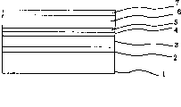
图8显示的是现有技术中包含有应变Si层的半导体衬底的截面示意图Figure 8 shows a schematic cross-sectional view of a semiconductor substrate comprising a strained Si layer in the prior art
具体实施方式Detailed ways
参照本发明中制造半导体衬底的方法,首先,在具有一个硅表面的衬底上依次形成第一缓冲Si层、第一应变SiGe层和第一Si层。此处,具有硅表面的衬底可以称作SOI、SOS衬底或者类似的称呼,其表面有一个单晶硅层,或者一个单晶硅衬底。衬底最好在对表面进行清洗以清除表面自然氧化膜后再进行使用。技术上任何认可的方法都可以在清洗步骤中使用。此处可以列出诸如沸腾的硫酸、RCA清洗和(或者)使用氟酸进行酸洗这些不同的方法。Referring to the method for manufacturing a semiconductor substrate in the present invention, firstly, a first buffer Si layer, a first strained SiGe layer and a first Si layer are sequentially formed on a substrate having a silicon surface. Here, a substrate having a silicon surface may be referred to as an SOI, SOS substrate, or the like, the surface of which has a single-crystal silicon layer, or a single-crystal silicon substrate. The substrate is best used after cleaning the surface to remove the natural oxide film on the surface. Any technically recognized method may be used in the washing step. Different methods such as boiling sulfuric acid, RCA cleaning and/or pickling with hydrofluoric acid can be listed here.
第一缓冲硅层、第一应变SiGe层和第一Si层可以使用已知不同方法制造,诸如CVD法、溅射法、蒸汽沉积法或者MEB法。尤其优选使用CVD方法外延生长形成各层。在此情况下,制造环境可以使用领域内已知环境,特别是在大约界于400℃和650℃之间的温度比较适合薄膜成形。第一应变SiGe层和第一Si层必须以顺序的方式生成在上面所说明的三层之上。至于顺序薄膜成型的方法,能够在容器中切换材料气体以形成不同层的方法就比较合适。因此,在第一应变SiGe层和第一Si层分界面处的氧浓度就可以得以降低。The first buffer silicon layer, the first strained SiGe layer and the first Si layer can be fabricated using different known methods, such as CVD method, sputtering method, vapor deposition method or MEB method. In particular, it is preferable to form each layer by epitaxial growth using a CVD method. In this case, the manufacturing environment can be known in the art, especially a temperature between about 400°C and 650°C is suitable for film formation. The first strained SiGe layer and the first Si layer must be grown on top of the three layers explained above in a sequential manner. As for the method of sequential film forming, the method that can switch the material gas in the container to form different layers is more suitable. Therefore, the oxygen concentration at the interface between the first strained SiGe layer and the first Si layer can be reduced.
第一缓冲Si层的薄膜厚度优选的只要能够允许将带有硅表面的衬底的表面上存在的悬空键效应尽量降低到可能的水平即可,具体而言,第一缓冲Si层的优选厚度为10nm,或者更大。The film thickness of the first buffer Si layer is preferably as long as it can allow the dangling bond effect existing on the surface of the substrate with the silicon surface to be reduced to a possible level, specifically, the preferred thickness of the first buffer Si layer 10nm, or larger.
尽管第一应变SiGe层的Ge浓度没有特别的限定,但是Ge浓度可以大约位于比如10%和40%原子百分比之间,Ge的浓度优选的大致位于20%和30%原子百分比之间。SiGe的薄膜厚度最好不要大于临界薄膜厚度。临界薄膜厚度意思是指在SiGe薄膜沉积到衬底上时,其中SiGe薄膜开始发生点阵应变松弛时SiGe薄膜的薄膜厚度。具体而言,薄膜的厚度大约为500nm,或者更小,薄膜的厚度大约可以为5nm至500nm,优选的为10nm至300nm,其中具有上述说明Ge浓度的范围的SiGe层形成于硅衬底之上。此处,尽管Ge浓度可能以线性或者一具体的方式沿薄膜厚度的方向和层表面的方向改变,Ge浓度最好均匀。Although the Ge concentration of the first strained SiGe layer is not particularly limited, the Ge concentration may be approximately between, for example, 10% and 40 atomic%, and the Ge concentration is preferably approximately between 20% and 30 atomic%. The film thickness of SiGe is preferably not greater than the critical film thickness. The critical film thickness means the film thickness of the SiGe film at which lattice strain relaxation of the SiGe film begins to occur when the SiGe film is deposited on the substrate. Specifically, the thickness of the film is about 500nm, or less, and the thickness of the film may be about 5nm to 500nm, preferably 10nm to 300nm, wherein the SiGe layer having the range of Ge concentration described above is formed on the silicon substrate . Here, although the Ge concentration may vary linearly or in a specific manner in the direction of the film thickness and the direction of the layer surface, the Ge concentration is preferably uniform.
第一Si层的形成是为了在离子注入时不引入任何晶体缺陷,离子注入的目的是为了松弛第一应变SiGe层后续步骤中的应变,也是为了在诸如Si半导体层形成在SiGe层上时可以以上述清洗衬底表面同样的方法进行清洗。第一Si层最好为一单晶硅层。当SiGe薄膜中Ge浓度为30%时,薄膜在此情况下的优选厚度为20nm,或者更小。The formation of the first Si layer is in order not to introduce any crystal defects during ion implantation. The purpose of ion implantation is to relax the strain in the subsequent steps of the first strained SiGe layer, and also to be able to Cleaning is carried out in the same manner as above for cleaning the surface of the substrate. The first Si layer is preferably a single crystal silicon layer. When the Ge concentration in the SiGe thin film is 30%, the preferred thickness of the thin film in this case is 20 nm, or less.
离子随后注入所获衬底中,然后衬底进行退火。Ions are then implanted into the resulting substrate, which is then annealed.
离子种类最好满足这样的条件:离子的种类不允许晶体缺陷存在于其所通过的SiGe薄膜中;离子的种类在平均范围附近(注入峰值)引入晶体缺陷,核子阻断性能在离子停止的平均范围(Rp)正前方达到最大;离子种类电学上在下述包括回火工艺在内的工艺过程中,不对器件产生影响。比如,诸如硅、碳、锗第五族元素和诸如惰性气体氖、氦、氢都是典型的例子。尤其是,质量轻的轻金属是优选的。上述元素的离子注入时,如果不将离子注入区域转换为非晶区域,那么内埋晶体缺陷将会被引入到离子注入区域中。至于离子种类,氢或者氦是优选的,而氢是尤其优选的。The ion species preferably meet such conditions: the ion species does not allow crystal defects to exist in the SiGe film it passes through; the ion species introduces crystal defects near the average range (implantation peak), and the nucleon blocking performance is within the average value of the ion stop. The range (Rp) is maximized right ahead; the ionic species do not affect the device electrically during the following processes including the tempering process. For example, Group V elements such as silicon, carbon, and germanium, and noble gases such as neon, helium, and hydrogen are typical examples. In particular, light metals that are light in weight are preferred. During the ion implantation of the above elements, if the ion implantation area is not converted into an amorphous area, embedded crystal defects will be introduced into the ion implantation area. As ion species, hydrogen or helium is preferable, and hydrogen is especially preferable.
离子注入平均范围(Rp)最好深于SiGe薄膜的厚度。进一步的,如设置平均范围深于第一缓冲Si层、第一应变SiGe层和第一Si层的组合厚度将会产生很好的效果。也就是说,离子注入的平均范围设置深度位于第一Si层表面之下,这样,延展至SiGe薄膜表面的两个Si层中的晶体缺陷就会减少。相应的,将平均范围设置在界于第一Si层表面和第一Si层表面下50nm一位置之间的范围中是非常理想的。这样,离子注入加速能可以就使用的离子种类合理的调整到第一缓冲Si层的薄膜厚度、调整到第一应变SiGe层的薄膜厚度以及调整到第一Si层的薄膜厚度。比如在氢离子注入的情况下,注入能大约在10keV和50keV之间,优选的位于20keV和40keV之间。一次注入离子大约为1×1015cm-2至1×1017cm-2,优选的为1×1015cm-2至5×1016cm-2。The average range (Rp) of ion implantation is preferably deeper than the thickness of the SiGe film. Further, setting the average range deeper than the combined thickness of the first buffer Si layer, the first strained SiGe layer and the first Si layer will produce a good effect. That is to say, the average range setting depth of ion implantation is below the surface of the first Si layer, so that the crystal defects in the two Si layers extending to the surface of the SiGe film will be reduced. Accordingly, it is very desirable to set the average range in the range between the surface of the first Si layer and a position 50 nm below the surface of the first Si layer. In this way, the ion implantation acceleration energy can be reasonably adjusted to the film thickness of the first buffer Si layer, the film thickness of the first strained SiGe layer and the film thickness of the first Si layer according to the ion species used. For example in the case of hydrogen ion implantation, the implantation energy is approximately between 10 keV and 50 keV, preferably between 20 keV and 40 keV. The ion implanted at one time is about 1×10 15 cm -2 to 1×10 17 cm -2 , preferably 1×10 15 cm -2 to 5×10 16 cm -2 .
至于热处理,可以使用炉内退火、普通退火和RTA。热处理可以在诸如惰性气体(氩气或者类似)的氛围、标准氛围、氮气氛围、氧气氛围、氢气氛围中进行。至于具体条件,热处理可以在温度范围界于700℃和950℃之间加热10到30分钟。As for heat treatment, furnace annealing, ordinary annealing and RTA can be used. The heat treatment can be performed in an atmosphere such as an inert gas (argon or the like), a standard atmosphere, a nitrogen atmosphere, an oxygen atmosphere, a hydrogen atmosphere. As for specific conditions, the heat treatment may be performed at a temperature ranging between 700°C and 950°C for 10 to 30 minutes.
此处,相对于本发明,优选的在进行离子注入前在第一Si层上形成一个保护性薄膜。保护性薄膜的厚度和材料没有特别限制,既可以是绝缘薄膜也可以是半导体薄膜。具体而言,保护膜可以是热氧化薄膜、低温氧化薄膜(LTO薄膜)、高温氧化薄膜(HTO薄膜)、P-CVD制硅氧化薄膜和硅氮化物薄膜中的任何一种。至于包含薄膜的厚度比如大约为20nm至150nm。不仅如此,在退火后第二缓冲Si层形成前最好将保护膜去掉。技术内移除包含薄膜的通用方法是使用酸碱溶液湿腐蚀法、干腐蚀法或者类似方法。Here, with respect to the present invention, it is preferable to form a protective film on the first Si layer before ion implantation. The thickness and material of the protective film are not particularly limited, and it may be either an insulating film or a semiconductor film. Specifically, the protective film may be any of a thermal oxide film, a low temperature oxide film (LTO film), a high temperature oxide film (HTO film), a P-CVD silicon oxide film, and a silicon nitride film. As for the thickness of the containing film, for example, it is about 20nm to 150nm. Furthermore, it is preferable to remove the protective film before the formation of the second buffer Si layer after annealing. The common method of removing the containing film in the technology is to use the acid-base solution wet etching method, dry etching method or similar methods.
因此,第一应变SiGe层的点阵就可得以松弛,也就可以在第一Si层中提供拉应变。Therefore, the lattice of the first strained SiGe layer can be relaxed, and tensile strain can be provided in the first Si layer.
不仅如此,在本发明中最好在退火后下述第二缓冲Si层形成以前对第一Si层清洗以清除自然氧化物薄膜,最好减小第一Si层表面上的残余氧浓度。在上述说明的具有硅表面的衬底中所使用的同样方法可以作为此处的一种清洗方法。Furthermore, in the present invention, it is preferable to clean the first Si layer after annealing before formation of the second buffer Si layer described below to remove the native oxide film, and it is preferable to reduce the residual oxygen concentration on the surface of the first Si layer. The same method used in the above-described substrate having a silicon surface can be used as a cleaning method here.
第二缓冲Si层和第二SiGe层在所获衬底上顺序外延生长,进一步的,具有拉应变的第二Si层形成在第二SiGe层的表面。此处第二缓冲Si层、第二SiGe层和第二Si层可以使用与上述第一缓冲Si层、第一SiGe层和第一Si层相同的方法形成。此处,第二缓冲Si层和第二SiGe层顺序外延生长是必需的。第二缓冲Si层、第二SiGe层和第二Si层的形成厚度各自大约可以为5nm至20nm、100nm至300nm和5nm至20nm。The second buffer Si layer and the second SiGe layer are epitaxially grown sequentially on the obtained substrate, and further, the second Si layer with tensile strain is formed on the surface of the second SiGe layer. Here, the second buffer Si layer, the second SiGe layer, and the second Si layer can be formed using the same method as the above-mentioned first buffer Si layer, first SiGe layer, and first Si layer. Here, sequential epitaxial growth of the second buffer Si layer and the second SiGe layer is necessary. The second buffer Si layer, the second SiGe layer, and the second Si layer may each be formed to a thickness of approximately 5 nm to 20 nm, 100 nm to 300 nm, and 5 nm to 20 nm.
一个以此方式形成的半导体衬底其特征在于第一SiGe层和第一Si层、第一Si层和第二缓冲Si层,以及(或者)第二缓冲Si层和第二SiGe层的分界面处的氧浓度非常低。也就是说,在至少其中之一的分界面上的残余氧浓度大约为1×1016cm-3或者更少,而每一个分界面处的残余氧浓度优选的为1×1016cm-3或者更少,所有分界面处的残余氧浓度总和不超过1×1016cm-3或者更少时更好。在这些情况下,由于第一和第二SiGe层分界面间的残余氧而导致第二Si层和第二SiGe层结晶性能恶化以及由此导致漏电流的增加都可以被有效的防止。A semiconductor substrate formed in this way is characterized by the interface between the first SiGe layer and the first Si layer, the first Si layer and the second buffer Si layer, and (or) the second buffer Si layer and the second SiGe layer The oxygen concentration is very low. That is, the residual oxygen concentration at at least one of the interfaces is about 1×10 16 cm -3 or less, and the residual oxygen concentration at each interface is preferably 1×10 16 cm -3 or less, and it is better when the sum of the residual oxygen concentrations at all interfaces does not exceed 1×10 16 cm -3 or less. In these cases, deterioration of crystallization properties of the second Si layer and the second SiGe layer due to residual oxygen at the interface between the first and second SiGe layers and thus an increase in leakage current can be effectively prevented.
如上所述之半导体衬底可以通过实施和传统半导体工艺相同的工艺而作为各种不同半导体器件(比如NMOS、PMOS、CMOS晶体三极管、闪存晶体三极管)的衬底。这些工艺包括元素隔离区的形成、门绝缘薄膜和门电极的形成、LDD或者DDD区或者源极/漏极区的形成、中间层绝缘薄膜的形成、配线层的形成以及其它类似的工艺。The above-mentioned semiconductor substrate can be used as the substrate of various semiconductor devices (such as NMOS, PMOS, CMOS transistor, and flash memory transistor) by implementing the same process as the traditional semiconductor process. These processes include the formation of element isolation regions, the formation of gate insulating films and gate electrodes, the formation of LDD or DDD regions or source/drain regions, the formation of interlayer insulating films, the formation of wiring layers and other similar processes.
具体而言,MOS晶体三极管由位于半导体衬底的通过门绝缘薄膜第二Si层的门电极和半导体衬底第二Si层边表面层上的源极/漏极构成。此处,门绝缘薄膜和门电极可以通过选择合适的材料、尺寸、加工方法和其它业内已知的方法来形成。半导体衬底最好加入杂质以调整衬底的抵抗性能或类似的性能。至于此处的浓度,比如,杂质浓度可以大约为1×1017cm-3至1×1018cm-3。源/漏极的形成也可以通过合适的选择传统中所需形成此类半导体器件的杂质浓度、结深度等。比如,杂质浓度大约为1×1019cm-3至1×1021cm-3而结深度大约为50nm至200nm。不仅如此,半导体衬底中第一SiGe层和第二SiGe层的组合薄膜厚度优选设置数值至少为此类半导体器件耗尽层的深度,耗尽层在漏极上通电压时扩展。此处漏极电压没有特别限制,比如,优选的大约位于1.0V至5.0V之间。Specifically, the MOS transistor is composed of a gate electrode located on the second Si layer of the gate insulating film of the semiconductor substrate and a source/drain electrode on the surface layer of the second Si layer of the semiconductor substrate. Here, the gate insulating film and the gate electrode can be formed by selecting appropriate materials, dimensions, processing methods and other methods known in the art. The semiconductor substrate is preferably doped with impurities to adjust the resistance of the substrate or the like. As for the concentration here, for example, the impurity concentration may be approximately 1×10 17 cm −3 to 1×10 18 cm −3 . The source/drain can also be formed by properly selecting the impurity concentration, junction depth, etc. required to form such a semiconductor device in the conventional. For example, the impurity concentration is about 1×10 19 cm −3 to 1×10 21 cm −3 and the junction depth is about 50 nm to 200 nm. Furthermore, the combined film thickness of the first SiGe layer and the second SiGe layer in the semiconductor substrate is preferably set to be at least the depth of the depletion layer of such semiconductor devices, which expands when a voltage is applied to the drain. Here, the drain voltage is not particularly limited, for example, it is preferably approximately between 1.0V and 5.0V.
如上所述,电子或者空穴的移动性能可以增加,这样驱动性能也会提高,尤其是在第一SiGe层和第二SiGe层的组合薄膜厚度大于耗尽层的深度时,或者说,在产生的耗尽层其宽度小于第一SiGe层和第二SiGe层的组合薄膜厚度的情况下也是这样的。As mentioned above, the mobile performance of electrons or holes can be increased, so the driving performance will also be improved, especially when the combined film thickness of the first SiGe layer and the second SiGe layer is greater than the depth of the depletion layer, or in other words, when the This is also the case where the width of the depletion layer is smaller than the combined film thickness of the first SiGe layer and the second SiGe layer.
下面,将对本发明中生产半导体衬底方法,半导体衬底和半导体器件的优选实施例参照图纸进行详细说明。Hereinafter, preferred embodiments of a method for producing a semiconductor substrate, a semiconductor substrate, and a semiconductor device in the present invention will be described in detail with reference to the drawings.
本发明的半导体衬底以下述顺序包括第一缓冲Si层2、其中的应变已经被松弛的第一SiGe层3、有拉应变的第一Si层4、第二缓冲Si层5、第二SiGe层6和有拉应变的第二Si层7位于硅衬底1之上,如图1所示。不仅如此,第一SiGe层3和第一Si层4分界面处、第一Si层4和第一缓冲Si层5分界面处以及第二缓冲Si层5和第二SiGe层6分界面处的氧浓度维持很低的水平。The semiconductor substrate of the present invention includes, in the following order, a first
上述半导体衬底可以以下述的方法形成。The aforementioned semiconductor substrate can be formed by the following method.
首先,如图2(a)中所示,进行硫酸煮和RCA清洗,而且,p型硅(100)衬底1表面上的自然氧化薄膜使用5%的稀释硫酸去除。First, as shown in FIG. 2(a), sulfuric acid boiling and RCA cleaning are performed, and the natural oxide film on the surface of p-type silicon (100)
第二,如图2(b)中所示,第一缓冲Si层2在硅衬底1上使用低压化学蒸汽沉积单元外延生长厚度达到5nm。此缓冲Si层2形成的原因是为了尽可能限制在对硅衬底1进行预处理(硫酸煮、RCA清洗和5%稀释硫酸工艺)后存在于硅衬底1表面上的悬空键效应。然后,Ge浓度为30%的第一SiGe层3外延生长至厚度为150nm,第一Si层4外延增长至薄膜厚度为5nm,两者使用锗烷(GeH4)和硅烷(SiH4)顺序进行。也就是说,此处进行第一缓冲Si层2、第一SiGe层3和第一Si层4顺序薄膜成形。此处第一SiGe层的薄膜厚度不超过临界薄膜厚度。而且,第一Si层4顺序外延增长至厚度为5nm,因为必须减小第一SiGe层3和后面将要形成的第二SiGe层6分界面处的残余氧。第一Si层6的表面的优点是即使在氢离子注入步骤后也可以使用传统Si衬底的清洗步骤。Second, as shown in FIG. 2( b ), the first
接着,如图2(c)中所示,氧化薄膜8作为污染物阻止薄膜而形成厚度有20nm,氢离子在注入能为18keV,注入量为3×10¹⁶H+/cm2和倾斜角为7°时注入。Next, as shown in FIG. 2(c), the
此后,如图2(d)中所示,氧化薄膜8被移出,并在N2环境中、800℃下退火10分钟。XRD分析表明这种退火使得第一SiGe层的点阵应变充分松弛。而且,第一SiGe层3的表面点阵应变松弛后,使用Nomarski显微镜观察发现表面光滑而不粗糙。第一SiGe层3的点阵应变在上述情况下充分松弛,结晶性能非常好。Thereafter, as shown in FIG. 2(d), the
下面,所获的衬底1的第一Si层4表面使用5%稀释硫酸处理,也进行超纯净水清洗处理。接着,如图2(e)中所示,第二缓冲Si层5使用低压化学蒸发单元外延增长至厚度为5nm。此层沉积的原因和上述缓冲Si层2相同。进一步的,Ge浓度为30%的第二SiGe层6外延增长至厚度为150nm,第二Si层7外延增长至薄膜厚度20nm,两者使用锗烷(GeH4)和硅烷(SiH4)顺序进行。就是说,此处进行第二缓冲Si层、第二SiGe层和第二Si层顺序薄膜成形。Next, the surface of the
如图3中所示SiGe-CMOS(应变Si-CMOS)晶体三极管使用上述半导体衬底(图3中只显示了一个MOS晶体三极管)制造。A SiGe-CMOS (strained Si-CMOS) transistor as shown in FIG. 3 is manufactured using the above-mentioned semiconductor substrate (only one MOS transistor is shown in FIG. 3 ).
在此CMOS晶体三极管中,门电极12使用领域中常用方法通过一个门绝缘薄膜11形成在半导体衬底之上,门电极的侧壁间隔基13位于侧壁之上。不仅如此,源/漏极10和9以自对齐的方式、并和门电极12相对形成于第二Si层6边的半导体衬底的表面层上。杂质均匀的掺入到(比如,大约为4×1017cm-3)组成此MOS晶体三极管半导体衬底的各半导体层中(也就是说,第一缓冲Si层2、其中应变已经松弛的第一SiGe层3、第一Si层4、第二缓冲Si层5、第二SiGe层6和具有拉应变的第二Si层7),以获得一定的阻值。而且,杂质浓度和源/漏极10和9的结深数值设为至少为1×1021cm-3和约110nm。In this CMOS transistor, the gate electrode 12 is formed on the semiconductor substrate through a gate insulating film 11 by a common method in the field, and the sidewall spacer 13 of the gate electrode is located on the sidewall. Furthermore, source/drain electrodes 10 and 9 are formed on the surface layer of the semiconductor substrate at the side of the
耗尽层14以上述方式并在漏极9上通入2.5V的电压形成于CMOS晶体三极管上。此耗尽层14的范围(比如,大约140nm)不大于第一SiGe层3(薄膜厚度为150nm)和第二SiGe层6(薄膜厚度为150nm)的组合薄膜厚度。The
对具有此特性的CMOS晶体三极管进行了评估。结果显示在图4(a)-(b)与图5(a)-(b)中。CMOS transistors with this characteristic were evaluated. The results are shown in Fig. 4(a)-(b) and Fig. 5(a)-(b).
使用本发明半导体器件的应变Si-NMOS(SiGe NMOS)晶体三极管Id-Vd特性(参看图4(a))和Gm特性(参看图4(b))在图4(a)和图4(b)中进行了比较。此处,图4(a)和图4(b)中第二SiGe层中Ge的有效浓度为16%。Ge的有效浓度显示数值为实际形成SiGe层中Ge浓度乘以SiGe的松弛比例。使用本发明半导体器件的应变Si-PMOS(SiGe PMOS)晶体三极管和使用传统Si衬底制造PMOS晶体三极管的Id-Vd特性(如图5(a))和Gm特性(参看图5(b))在图5(a)和图5(b)中进行了比较。在图5(a)和5(b)中的第二SiGe层的有效Ge浓度为24%。Use strained Si-NMOS (SiGe NMOS) transistor Id-Vd characteristic (referring to Fig. 4 (a)) and Gm characteristic (referring to Fig. 4 (b)) of the strained Si-NMOS (SiGe NMOS) transistor of semiconductor device of the present invention in Fig. 4 (a) and Fig. 4 (b) ) for comparison. Here, the effective concentration of Ge in the second SiGe layer in FIG. 4(a) and FIG. 4(b) is 16%. The displayed value of the effective concentration of Ge is the Ge concentration in the actually formed SiGe layer multiplied by the relaxation ratio of SiGe. Use the strained Si-PMOS (SiGe PMOS) transistor of semiconductor device of the present invention and use the Id-Vd characteristic (as Fig. 5 (a)) and Gm characteristic (referring to Fig. 5 (b)) of traditional Si substrate to manufacture PMOS transistor triode A comparison is made in Figure 5(a) and Figure 5(b). The effective Ge concentration of the second SiGe layer in Figures 5(a) and 5(b) is 24%.
从图4(a)和图4(b)中可知,对于Id-Vd特性而言,应变Si-NMOS或者PMOS晶体三极管的驱动性能都有所提高。不仅如此,从图5(a)和图5(b)中可以看出相对Gm特性而言,应变Si-NMOS或者PMOS晶体三极管的移动性能都有所提高。It can be seen from Fig. 4(a) and Fig. 4(b) that, for Id-Vd characteristics, the driving performance of strained Si-NMOS or PMOS transistors has been improved. Not only that, it can be seen from Figure 5(a) and Figure 5(b) that relative to the Gm characteristics, the mobile performance of the strained Si-NMOS or PMOS transistors has been improved.
而且,测量结果表明,和使用传统Si衬底制造的MOS晶体三极管相比,本发明应变Si-MOS晶体三极管中由于氧峰值浓度的原因而导致的结漏电流的减小不止一个数量级。经过证明,这种减小是由于上述说明之半导体衬底生产步骤中氧峰值浓度的减小引起的。Moreover, the measurement results show that, compared with the MOS transistor manufactured using the traditional Si substrate, the junction leakage current caused by the oxygen peak concentration in the strained Si-MOS transistor of the present invention is reduced by more than one order of magnitude. It was confirmed that this reduction was caused by the reduction of the oxygen peak concentration in the semiconductor substrate production steps described above.
本发明中影响结晶性的第一SiGe层和第二SiGe层间的残余氧可以被减小。因此,这就有可能通过减小SiGe层中穿透位错密度,来生产一种具有良好结晶性能的应变Si层/应变释放SiGe层半导体衬底。Residual oxygen between the first SiGe layer and the second SiGe layer, which affects crystallinity, can be reduced in the present invention. Therefore, it is possible to produce a strained Si layer/strain relieved SiGe layer semiconductor substrate with good crystallinity by reducing the threading dislocation density in the SiGe layer.
不仅如此,第二缓冲层和第一Si层间残余氧浓度可以通过在形成第二缓冲层前清洗第一Si层的表面来进一步减小,这样就可以获得具有很好结晶性能的半导体衬底。尤其是在第一SiGe层和第一Si层、第一Si层和第二缓冲Si层,以及(或者)第二缓冲Si层和第二SiGe层的分界面处的氧浓度小于1×1016cm-3时,这种效果就非常明显。Not only that, the residual oxygen concentration between the second buffer layer and the first Si layer can be further reduced by cleaning the surface of the first Si layer before forming the second buffer layer, so that a semiconductor substrate with good crystallization properties can be obtained . Especially the oxygen concentration at the interface between the first SiGe layer and the first Si layer, the first Si layer and the second buffer Si layer, and (or) the second buffer Si layer and the second SiGe layer is less than 1×10 16 When cm -3 , this effect is very obvious.
进一步的,第一SiGe层中不会引入晶体缺陷,点阵应变在第一SiGe层的形成厚度不超过临界薄膜厚度的情况下可得以充分松弛,这样就可以获得一个高性能的半导体器件,其中晶体缺陷数目被进一步降低。Further, crystal defects are not introduced into the first SiGe layer, and the lattice strain can be fully relaxed when the thickness of the first SiGe layer does not exceed the critical film thickness, so that a high-performance semiconductor device can be obtained, wherein The number of crystal defects is further reduced.
不仅如此,在使用上述半导体衬底的半导体器件中以及在第一SiGe层和第二SiGe层的组合薄膜厚度至少为耗尽层的厚度时,电子或空穴的移动性能够增加,耗尽层在给漏极通电后扩展。不仅如此,这也同样可以提高半导体器件的驱动性能。这样,就可能获得高性能的半导体器件。Furthermore, in the semiconductor device using the above-mentioned semiconductor substrate and when the combined film thickness of the first SiGe layer and the second SiGe layer is at least the thickness of the depletion layer, the mobility of electrons or holes can be increased, and the depletion layer expands after energizing the drain. Not only that, but it can also improve the driving performance of the semiconductor device. Thus, it is possible to obtain a high-performance semiconductor device.
Claims (11)
Applications Claiming Priority (2)
| Application Number | Priority Date | Filing Date | Title |
|---|---|---|---|
| JP2002263158 | 2002-09-09 | ||
| JP2002263158A JP2004103805A (en) | 2002-09-09 | 2002-09-09 | Semiconductor substrate manufacturing method, semiconductor substrate and semiconductor device |
Publications (2)
| Publication Number | Publication Date |
|---|---|
| CN1487565A true CN1487565A (en) | 2004-04-07 |
| CN1259694C CN1259694C (en) | 2006-06-14 |
Family
ID=32089100
Family Applications (1)
| Application Number | Title | Priority Date | Filing Date |
|---|---|---|---|
| CNB031562779A Expired - Fee Related CN1259694C (en) | 2002-09-09 | 2003-09-02 | Semiconductor substrate production method, semiconductor substrate and semiconductor device |
Country Status (4)
| Country | Link |
|---|---|
| US (1) | US6869897B2 (en) |
| JP (1) | JP2004103805A (en) |
| CN (1) | CN1259694C (en) |
| TW (1) | TWI234811B (en) |
Cited By (4)
| Publication number | Priority date | Publication date | Assignee | Title |
|---|---|---|---|---|
| CN100517609C (en) * | 2004-09-09 | 2009-07-22 | 国际商业机器公司 | Method for making silicide on the surface of SiGe-containing substrate |
| CN101228616B (en) * | 2005-07-22 | 2010-10-20 | 加利福尼亚大学董事会 | Method for controlling dislocation location in silicon germanium buffer layer and article produced |
| US7838934B2 (en) | 2004-12-31 | 2010-11-23 | Dongbu Electronics Co., Ltd. | Semiconductor device and method for manufacturing the same |
| CN102737963A (en) * | 2012-07-20 | 2012-10-17 | 中国科学院上海微系统与信息技术研究所 | Method for preparing semiconductor material through ion injection and fixed-point adsorption technologies |
Families Citing this family (11)
| Publication number | Priority date | Publication date | Assignee | Title |
|---|---|---|---|---|
| KR100605504B1 (en) * | 2003-07-30 | 2006-07-28 | 삼성전자주식회사 | A semiconductor device comprising an epitaxial layer having a low dislocation density and a method of manufacturing the semiconductor device |
| GB0424290D0 (en) * | 2004-11-02 | 2004-12-01 | Koninkl Philips Electronics Nv | Method of growing a strained layer |
| US7229901B2 (en) * | 2004-12-16 | 2007-06-12 | Wisconsin Alumni Research Foundation | Fabrication of strained heterojunction structures |
| JP4613656B2 (en) * | 2005-03-22 | 2011-01-19 | 信越半導体株式会社 | Manufacturing method of semiconductor wafer |
| US7772635B2 (en) | 2005-10-27 | 2010-08-10 | Micron Technology, Inc. | Non-volatile memory device with tensile strained silicon layer |
| JP5141029B2 (en) | 2007-02-07 | 2013-02-13 | 富士通セミコンダクター株式会社 | Semiconductor device and manufacturing method thereof |
| JP2010171337A (en) * | 2009-01-26 | 2010-08-05 | Toshiba Corp | Field effect transistor |
| JP5067381B2 (en) * | 2009-02-19 | 2012-11-07 | 東京エレクトロン株式会社 | Operation method of heat treatment equipment |
| US8361868B2 (en) * | 2010-04-28 | 2013-01-29 | Acorn Technologies, Inc. | Transistor with longitudinal strain in channel induced by buried stressor relaxed by implantation |
| CN103632930B (en) * | 2012-08-28 | 2016-06-15 | 中国科学院上海微系统与信息技术研究所 | Utilize superthin layer absorption to prepare the method for ultrathin modified material on insulator |
| WO2015064338A1 (en) | 2013-10-31 | 2015-05-07 | 独立行政法人科学技術振興機構 | Semiconductor-substrate manufacturing method and semiconductor-device manufacturing method in which germanium layer is heat-treated |
Family Cites Families (6)
| Publication number | Priority date | Publication date | Assignee | Title |
|---|---|---|---|---|
| US5534713A (en) * | 1994-05-20 | 1996-07-09 | International Business Machines Corporation | Complementary metal-oxide semiconductor transistor logic using strained SI/SIGE heterostructure layers |
| US6593641B1 (en) * | 2001-03-02 | 2003-07-15 | Amberwave Systems Corporation | Relaxed silicon germanium platform for high speed CMOS electronics and high speed analog circuits |
| US6746902B2 (en) * | 2002-01-31 | 2004-06-08 | Sharp Laboratories Of America, Inc. | Method to form relaxed sige layer with high ge content |
| US6562703B1 (en) * | 2002-03-13 | 2003-05-13 | Sharp Laboratories Of America, Inc. | Molecular hydrogen implantation method for forming a relaxed silicon germanium layer with high germanium content |
| US6793731B2 (en) * | 2002-03-13 | 2004-09-21 | Sharp Laboratories Of America, Inc. | Method for recrystallizing an amorphized silicon germanium film overlying silicon |
| US6703293B2 (en) * | 2002-07-11 | 2004-03-09 | Sharp Laboratories Of America, Inc. | Implantation at elevated temperatures for amorphization re-crystallization of Si1-xGex films on silicon substrates |
-
2002
- 2002-09-09 JP JP2002263158A patent/JP2004103805A/en active Pending
-
2003
- 2003-09-02 CN CNB031562779A patent/CN1259694C/en not_active Expired - Fee Related
- 2003-09-05 TW TW092124657A patent/TWI234811B/en not_active IP Right Cessation
- 2003-09-05 US US10/655,556 patent/US6869897B2/en not_active Expired - Fee Related
Cited By (5)
| Publication number | Priority date | Publication date | Assignee | Title |
|---|---|---|---|---|
| CN100517609C (en) * | 2004-09-09 | 2009-07-22 | 国际商业机器公司 | Method for making silicide on the surface of SiGe-containing substrate |
| US7838934B2 (en) | 2004-12-31 | 2010-11-23 | Dongbu Electronics Co., Ltd. | Semiconductor device and method for manufacturing the same |
| CN101228616B (en) * | 2005-07-22 | 2010-10-20 | 加利福尼亚大学董事会 | Method for controlling dislocation location in silicon germanium buffer layer and article produced |
| CN102737963A (en) * | 2012-07-20 | 2012-10-17 | 中国科学院上海微系统与信息技术研究所 | Method for preparing semiconductor material through ion injection and fixed-point adsorption technologies |
| CN102737963B (en) * | 2012-07-20 | 2015-03-18 | 中国科学院上海微系统与信息技术研究所 | Method for preparing semiconductor material through ion injection and fixed-point adsorption technologies |
Also Published As
| Publication number | Publication date |
|---|---|
| US6869897B2 (en) | 2005-03-22 |
| JP2004103805A (en) | 2004-04-02 |
| CN1259694C (en) | 2006-06-14 |
| TW200414312A (en) | 2004-08-01 |
| TWI234811B (en) | 2005-06-21 |
| US20040075106A1 (en) | 2004-04-22 |
Similar Documents
| Publication | Publication Date | Title |
|---|---|---|
| JP3970011B2 (en) | Semiconductor device and manufacturing method thereof | |
| CN1265431C (en) | Relaxed, low-defect SiGe-on-insulator and its fabrication method | |
| JP4446424B2 (en) | Method for manufacturing relaxed SiGe substrate | |
| CN1241238C (en) | Method for producing semiconductor substrate | |
| TWI740249B (en) | Method for making a semiconductor device including a superlattice having nitrogen diffused therein | |
| CN1263089C (en) | Method for mfg. semiconductor substrate | |
| US7615471B2 (en) | Method for producing a tensioned layer on a substrate, and a layer structure | |
| CN1168147C (en) | Manufacturing method of semiconductor crystal | |
| CN1467795A (en) | Manufacturing method of semiconductor substrate and manufacturing method of semiconductor device | |
| CN1615541A (en) | Method of creating high-quality relaxed SiGe-on-insulator for strained SiCMOS applications | |
| CN1574395A (en) | Gate-induced strain for mos performance improvement | |
| CN1487565A (en) | Semiconductor substrate production method, semiconductor substrate and semiconductor device | |
| CN1656603A (en) | Forming lattice-tuned semiconductor substrates | |
| CN1770391A (en) | Semiconductor structure and manufacturing method thereof | |
| KR20070059157A (en) | Method of manufacturing a semiconductor wafer | |
| JP2003249641A (en) | Semiconductor substrate, method of manufacturing the same, and semiconductor device | |
| CN100350561C (en) | Method for fabricating SIGE substrate materials on metastable insulator and substrate materials | |
| CN1622294A (en) | Method of improving the quality of defective semiconductor material | |
| US7187059B2 (en) | Compressive SiGe <110> growth and structure of MOSFET devices | |
| CN1894775A (en) | Method for forming a strained Si-channel in a MOFSET structure | |
| CN1957458A (en) | Formation of silicon-germanium-on-insulator structures by oxidizing and burying porous silicon layers | |
| JP3488914B2 (en) | Semiconductor device manufacturing method | |
| JP3933405B2 (en) | Semiconductor substrate, semiconductor device and manufacturing method thereof | |
| CN1284216C (en) | Field effect transistor structure with tensile strained channel layer and method of manufacturing the same | |
| JP2003282471A (en) | Method for manufacturing semiconductor substrate |
Legal Events
| Date | Code | Title | Description |
|---|---|---|---|
| C06 | Publication | ||
| PB01 | Publication | ||
| C10 | Entry into substantive examination | ||
| SE01 | Entry into force of request for substantive examination | ||
| C14 | Grant of patent or utility model | ||
| GR01 | Patent grant | ||
| C17 | Cessation of patent right | ||
| CF01 | Termination of patent right due to non-payment of annual fee |
Granted publication date: 20060614 Termination date: 20130902 |