CN1411055A - Wiring substrate for small electronic unit and mfg. method thereof - Google Patents
Wiring substrate for small electronic unit and mfg. method thereof Download PDFInfo
- Publication number
- CN1411055A CN1411055A CN02143438A CN02143438A CN1411055A CN 1411055 A CN1411055 A CN 1411055A CN 02143438 A CN02143438 A CN 02143438A CN 02143438 A CN02143438 A CN 02143438A CN 1411055 A CN1411055 A CN 1411055A
- Authority
- CN
- China
- Prior art keywords
- insulated substrate
- conductive
- conductive ridges
- electronic component
- circuit board
- Prior art date
- Legal status (The legal status is an assumption and is not a legal conclusion. Google has not performed a legal analysis and makes no representation as to the accuracy of the status listed.)
- Pending
Links
Images


Classifications
-
- H—ELECTRICITY
- H01—ELECTRIC ELEMENTS
- H01L—SEMICONDUCTOR DEVICES NOT COVERED BY CLASS H10
- H01L24/00—Arrangements for connecting or disconnecting semiconductor or solid-state bodies; Methods or apparatus related thereto
- H01L24/93—Batch processes
- H01L24/95—Batch processes at chip-level, i.e. with connecting carried out on a plurality of singulated devices, i.e. on diced chips
- H01L24/97—Batch processes at chip-level, i.e. with connecting carried out on a plurality of singulated devices, i.e. on diced chips the devices being connected to a common substrate, e.g. interposer, said common substrate being separable into individual assemblies after connecting
-
- H—ELECTRICITY
- H05—ELECTRIC TECHNIQUES NOT OTHERWISE PROVIDED FOR
- H05K—PRINTED CIRCUITS; CASINGS OR CONSTRUCTIONAL DETAILS OF ELECTRIC APPARATUS; MANUFACTURE OF ASSEMBLAGES OF ELECTRICAL COMPONENTS
- H05K3/00—Apparatus or processes for manufacturing printed circuits
- H05K3/10—Apparatus or processes for manufacturing printed circuits in which conductive material is applied to the insulating support in such a manner as to form the desired conductive pattern
-
- H—ELECTRICITY
- H01—ELECTRIC ELEMENTS
- H01L—SEMICONDUCTOR DEVICES NOT COVERED BY CLASS H10
- H01L23/00—Details of semiconductor or other solid state devices
- H01L23/48—Arrangements for conducting electric current to or from the solid state body in operation, e.g. leads, terminal arrangements ; Selection of materials therefor
- H01L23/488—Arrangements for conducting electric current to or from the solid state body in operation, e.g. leads, terminal arrangements ; Selection of materials therefor consisting of soldered or bonded constructions
- H01L23/498—Leads, i.e. metallisations or lead-frames on insulating substrates, e.g. chip carriers
- H01L23/49822—Multilayer substrates
-
- H—ELECTRICITY
- H01—ELECTRIC ELEMENTS
- H01L—SEMICONDUCTOR DEVICES NOT COVERED BY CLASS H10
- H01L23/00—Details of semiconductor or other solid state devices
- H01L23/48—Arrangements for conducting electric current to or from the solid state body in operation, e.g. leads, terminal arrangements ; Selection of materials therefor
- H01L23/488—Arrangements for conducting electric current to or from the solid state body in operation, e.g. leads, terminal arrangements ; Selection of materials therefor consisting of soldered or bonded constructions
- H01L23/498—Leads, i.e. metallisations or lead-frames on insulating substrates, e.g. chip carriers
- H01L23/49838—Geometry or layout
-
- H—ELECTRICITY
- H01—ELECTRIC ELEMENTS
- H01L—SEMICONDUCTOR DEVICES NOT COVERED BY CLASS H10
- H01L24/00—Arrangements for connecting or disconnecting semiconductor or solid-state bodies; Methods or apparatus related thereto
- H01L24/01—Means for bonding being attached to, or being formed on, the surface to be connected, e.g. chip-to-package, die-attach, "first-level" interconnects; Manufacturing methods related thereto
- H01L24/26—Layer connectors, e.g. plate connectors, solder or adhesive layers; Manufacturing methods related thereto
- H01L24/31—Structure, shape, material or disposition of the layer connectors after the connecting process
- H01L24/32—Structure, shape, material or disposition of the layer connectors after the connecting process of an individual layer connector
-
- H—ELECTRICITY
- H05—ELECTRIC TECHNIQUES NOT OTHERWISE PROVIDED FOR
- H05K—PRINTED CIRCUITS; CASINGS OR CONSTRUCTIONAL DETAILS OF ELECTRIC APPARATUS; MANUFACTURE OF ASSEMBLAGES OF ELECTRICAL COMPONENTS
- H05K1/00—Printed circuits
- H05K1/02—Details
- H05K1/11—Printed elements for providing electric connections to or between printed circuits
- H05K1/111—Pads for surface mounting, e.g. lay-out
- H05K1/112—Pads for surface mounting, e.g. lay-out directly combined with via connections
- H05K1/113—Via provided in pad; Pad over filled via
-
- H—ELECTRICITY
- H05—ELECTRIC TECHNIQUES NOT OTHERWISE PROVIDED FOR
- H05K—PRINTED CIRCUITS; CASINGS OR CONSTRUCTIONAL DETAILS OF ELECTRIC APPARATUS; MANUFACTURE OF ASSEMBLAGES OF ELECTRICAL COMPONENTS
- H05K1/00—Printed circuits
- H05K1/02—Details
- H05K1/11—Printed elements for providing electric connections to or between printed circuits
- H05K1/115—Via connections; Lands around holes or via connections
- H05K1/116—Lands, clearance holes or other lay-out details concerning the surrounding of a via
-
- H—ELECTRICITY
- H01—ELECTRIC ELEMENTS
- H01L—SEMICONDUCTOR DEVICES NOT COVERED BY CLASS H10
- H01L2224/00—Indexing scheme for arrangements for connecting or disconnecting semiconductor or solid-state bodies and methods related thereto as covered by H01L24/00
- H01L2224/01—Means for bonding being attached to, or being formed on, the surface to be connected, e.g. chip-to-package, die-attach, "first-level" interconnects; Manufacturing methods related thereto
- H01L2224/02—Bonding areas; Manufacturing methods related thereto
- H01L2224/04—Structure, shape, material or disposition of the bonding areas prior to the connecting process
- H01L2224/05—Structure, shape, material or disposition of the bonding areas prior to the connecting process of an individual bonding area
- H01L2224/0554—External layer
- H01L2224/05599—Material
-
- H—ELECTRICITY
- H01—ELECTRIC ELEMENTS
- H01L—SEMICONDUCTOR DEVICES NOT COVERED BY CLASS H10
- H01L2224/00—Indexing scheme for arrangements for connecting or disconnecting semiconductor or solid-state bodies and methods related thereto as covered by H01L24/00
- H01L2224/01—Means for bonding being attached to, or being formed on, the surface to be connected, e.g. chip-to-package, die-attach, "first-level" interconnects; Manufacturing methods related thereto
- H01L2224/02—Bonding areas; Manufacturing methods related thereto
- H01L2224/04—Structure, shape, material or disposition of the bonding areas prior to the connecting process
- H01L2224/06—Structure, shape, material or disposition of the bonding areas prior to the connecting process of a plurality of bonding areas
- H01L2224/0601—Structure
- H01L2224/0603—Bonding areas having different sizes, e.g. different heights or widths
-
- H—ELECTRICITY
- H01—ELECTRIC ELEMENTS
- H01L—SEMICONDUCTOR DEVICES NOT COVERED BY CLASS H10
- H01L2224/00—Indexing scheme for arrangements for connecting or disconnecting semiconductor or solid-state bodies and methods related thereto as covered by H01L24/00
- H01L2224/01—Means for bonding being attached to, or being formed on, the surface to be connected, e.g. chip-to-package, die-attach, "first-level" interconnects; Manufacturing methods related thereto
- H01L2224/26—Layer connectors, e.g. plate connectors, solder or adhesive layers; Manufacturing methods related thereto
- H01L2224/31—Structure, shape, material or disposition of the layer connectors after the connecting process
- H01L2224/32—Structure, shape, material or disposition of the layer connectors after the connecting process of an individual layer connector
- H01L2224/321—Disposition
- H01L2224/32151—Disposition the layer connector connecting between a semiconductor or solid-state body and an item not being a semiconductor or solid-state body, e.g. chip-to-substrate, chip-to-passive
- H01L2224/32221—Disposition the layer connector connecting between a semiconductor or solid-state body and an item not being a semiconductor or solid-state body, e.g. chip-to-substrate, chip-to-passive the body and the item being stacked
- H01L2224/32225—Disposition the layer connector connecting between a semiconductor or solid-state body and an item not being a semiconductor or solid-state body, e.g. chip-to-substrate, chip-to-passive the body and the item being stacked the item being non-metallic, e.g. insulating substrate with or without metallisation
- H01L2224/32237—Disposition the layer connector connecting between a semiconductor or solid-state body and an item not being a semiconductor or solid-state body, e.g. chip-to-substrate, chip-to-passive the body and the item being stacked the item being non-metallic, e.g. insulating substrate with or without metallisation the layer connector connecting to a bonding area disposed in a recess of the surface of the item
-
- H—ELECTRICITY
- H01—ELECTRIC ELEMENTS
- H01L—SEMICONDUCTOR DEVICES NOT COVERED BY CLASS H10
- H01L2224/00—Indexing scheme for arrangements for connecting or disconnecting semiconductor or solid-state bodies and methods related thereto as covered by H01L24/00
- H01L2224/01—Means for bonding being attached to, or being formed on, the surface to be connected, e.g. chip-to-package, die-attach, "first-level" interconnects; Manufacturing methods related thereto
- H01L2224/42—Wire connectors; Manufacturing methods related thereto
- H01L2224/44—Structure, shape, material or disposition of the wire connectors prior to the connecting process
- H01L2224/45—Structure, shape, material or disposition of the wire connectors prior to the connecting process of an individual wire connector
- H01L2224/45001—Core members of the connector
- H01L2224/45099—Material
-
- H—ELECTRICITY
- H01—ELECTRIC ELEMENTS
- H01L—SEMICONDUCTOR DEVICES NOT COVERED BY CLASS H10
- H01L2224/00—Indexing scheme for arrangements for connecting or disconnecting semiconductor or solid-state bodies and methods related thereto as covered by H01L24/00
- H01L2224/01—Means for bonding being attached to, or being formed on, the surface to be connected, e.g. chip-to-package, die-attach, "first-level" interconnects; Manufacturing methods related thereto
- H01L2224/42—Wire connectors; Manufacturing methods related thereto
- H01L2224/47—Structure, shape, material or disposition of the wire connectors after the connecting process
- H01L2224/48—Structure, shape, material or disposition of the wire connectors after the connecting process of an individual wire connector
- H01L2224/481—Disposition
- H01L2224/48151—Connecting between a semiconductor or solid-state body and an item not being a semiconductor or solid-state body, e.g. chip-to-substrate, chip-to-passive
- H01L2224/48221—Connecting between a semiconductor or solid-state body and an item not being a semiconductor or solid-state body, e.g. chip-to-substrate, chip-to-passive the body and the item being stacked
- H01L2224/48225—Connecting between a semiconductor or solid-state body and an item not being a semiconductor or solid-state body, e.g. chip-to-substrate, chip-to-passive the body and the item being stacked the item being non-metallic, e.g. insulating substrate with or without metallisation
- H01L2224/48227—Connecting between a semiconductor or solid-state body and an item not being a semiconductor or solid-state body, e.g. chip-to-substrate, chip-to-passive the body and the item being stacked the item being non-metallic, e.g. insulating substrate with or without metallisation connecting the wire to a bond pad of the item
-
- H—ELECTRICITY
- H01—ELECTRIC ELEMENTS
- H01L—SEMICONDUCTOR DEVICES NOT COVERED BY CLASS H10
- H01L2224/00—Indexing scheme for arrangements for connecting or disconnecting semiconductor or solid-state bodies and methods related thereto as covered by H01L24/00
- H01L2224/01—Means for bonding being attached to, or being formed on, the surface to be connected, e.g. chip-to-package, die-attach, "first-level" interconnects; Manufacturing methods related thereto
- H01L2224/42—Wire connectors; Manufacturing methods related thereto
- H01L2224/47—Structure, shape, material or disposition of the wire connectors after the connecting process
- H01L2224/49—Structure, shape, material or disposition of the wire connectors after the connecting process of a plurality of wire connectors
- H01L2224/491—Disposition
- H01L2224/4912—Layout
- H01L2224/49171—Fan-out arrangements
-
- H—ELECTRICITY
- H01—ELECTRIC ELEMENTS
- H01L—SEMICONDUCTOR DEVICES NOT COVERED BY CLASS H10
- H01L2224/00—Indexing scheme for arrangements for connecting or disconnecting semiconductor or solid-state bodies and methods related thereto as covered by H01L24/00
- H01L2224/73—Means for bonding being of different types provided for in two or more of groups H01L2224/10, H01L2224/18, H01L2224/26, H01L2224/34, H01L2224/42, H01L2224/50, H01L2224/63, H01L2224/71
- H01L2224/732—Location after the connecting process
- H01L2224/73251—Location after the connecting process on different surfaces
- H01L2224/73265—Layer and wire connectors
-
- H—ELECTRICITY
- H01—ELECTRIC ELEMENTS
- H01L—SEMICONDUCTOR DEVICES NOT COVERED BY CLASS H10
- H01L2224/00—Indexing scheme for arrangements for connecting or disconnecting semiconductor or solid-state bodies and methods related thereto as covered by H01L24/00
- H01L2224/80—Methods for connecting semiconductor or other solid state bodies using means for bonding being attached to, or being formed on, the surface to be connected
- H01L2224/83—Methods for connecting semiconductor or other solid state bodies using means for bonding being attached to, or being formed on, the surface to be connected using a layer connector
- H01L2224/8338—Bonding interfaces outside the semiconductor or solid-state body
- H01L2224/83385—Shape, e.g. interlocking features
-
- H—ELECTRICITY
- H01—ELECTRIC ELEMENTS
- H01L—SEMICONDUCTOR DEVICES NOT COVERED BY CLASS H10
- H01L2224/00—Indexing scheme for arrangements for connecting or disconnecting semiconductor or solid-state bodies and methods related thereto as covered by H01L24/00
- H01L2224/80—Methods for connecting semiconductor or other solid state bodies using means for bonding being attached to, or being formed on, the surface to be connected
- H01L2224/85—Methods for connecting semiconductor or other solid state bodies using means for bonding being attached to, or being formed on, the surface to be connected using a wire connector
- H01L2224/8538—Bonding interfaces outside the semiconductor or solid-state body
- H01L2224/85399—Material
-
- H—ELECTRICITY
- H01—ELECTRIC ELEMENTS
- H01L—SEMICONDUCTOR DEVICES NOT COVERED BY CLASS H10
- H01L2224/00—Indexing scheme for arrangements for connecting or disconnecting semiconductor or solid-state bodies and methods related thereto as covered by H01L24/00
- H01L2224/93—Batch processes
- H01L2224/95—Batch processes at chip-level, i.e. with connecting carried out on a plurality of singulated devices, i.e. on diced chips
- H01L2224/97—Batch processes at chip-level, i.e. with connecting carried out on a plurality of singulated devices, i.e. on diced chips the devices being connected to a common substrate, e.g. interposer, said common substrate being separable into individual assemblies after connecting
-
- H—ELECTRICITY
- H01—ELECTRIC ELEMENTS
- H01L—SEMICONDUCTOR DEVICES NOT COVERED BY CLASS H10
- H01L24/00—Arrangements for connecting or disconnecting semiconductor or solid-state bodies; Methods or apparatus related thereto
- H01L24/01—Means for bonding being attached to, or being formed on, the surface to be connected, e.g. chip-to-package, die-attach, "first-level" interconnects; Manufacturing methods related thereto
- H01L24/42—Wire connectors; Manufacturing methods related thereto
- H01L24/47—Structure, shape, material or disposition of the wire connectors after the connecting process
- H01L24/48—Structure, shape, material or disposition of the wire connectors after the connecting process of an individual wire connector
-
- H—ELECTRICITY
- H01—ELECTRIC ELEMENTS
- H01L—SEMICONDUCTOR DEVICES NOT COVERED BY CLASS H10
- H01L24/00—Arrangements for connecting or disconnecting semiconductor or solid-state bodies; Methods or apparatus related thereto
- H01L24/01—Means for bonding being attached to, or being formed on, the surface to be connected, e.g. chip-to-package, die-attach, "first-level" interconnects; Manufacturing methods related thereto
- H01L24/42—Wire connectors; Manufacturing methods related thereto
- H01L24/47—Structure, shape, material or disposition of the wire connectors after the connecting process
- H01L24/49—Structure, shape, material or disposition of the wire connectors after the connecting process of a plurality of wire connectors
-
- H—ELECTRICITY
- H01—ELECTRIC ELEMENTS
- H01L—SEMICONDUCTOR DEVICES NOT COVERED BY CLASS H10
- H01L24/00—Arrangements for connecting or disconnecting semiconductor or solid-state bodies; Methods or apparatus related thereto
- H01L24/73—Means for bonding being of different types provided for in two or more of groups H01L24/10, H01L24/18, H01L24/26, H01L24/34, H01L24/42, H01L24/50, H01L24/63, H01L24/71
-
- H—ELECTRICITY
- H01—ELECTRIC ELEMENTS
- H01L—SEMICONDUCTOR DEVICES NOT COVERED BY CLASS H10
- H01L2924/00—Indexing scheme for arrangements or methods for connecting or disconnecting semiconductor or solid-state bodies as covered by H01L24/00
- H01L2924/0001—Technical content checked by a classifier
- H01L2924/00014—Technical content checked by a classifier the subject-matter covered by the group, the symbol of which is combined with the symbol of this group, being disclosed without further technical details
-
- H—ELECTRICITY
- H01—ELECTRIC ELEMENTS
- H01L—SEMICONDUCTOR DEVICES NOT COVERED BY CLASS H10
- H01L2924/00—Indexing scheme for arrangements or methods for connecting or disconnecting semiconductor or solid-state bodies as covered by H01L24/00
- H01L2924/01—Chemical elements
- H01L2924/01004—Beryllium [Be]
-
- H—ELECTRICITY
- H01—ELECTRIC ELEMENTS
- H01L—SEMICONDUCTOR DEVICES NOT COVERED BY CLASS H10
- H01L2924/00—Indexing scheme for arrangements or methods for connecting or disconnecting semiconductor or solid-state bodies as covered by H01L24/00
- H01L2924/01—Chemical elements
- H01L2924/01005—Boron [B]
-
- H—ELECTRICITY
- H01—ELECTRIC ELEMENTS
- H01L—SEMICONDUCTOR DEVICES NOT COVERED BY CLASS H10
- H01L2924/00—Indexing scheme for arrangements or methods for connecting or disconnecting semiconductor or solid-state bodies as covered by H01L24/00
- H01L2924/01—Chemical elements
- H01L2924/01006—Carbon [C]
-
- H—ELECTRICITY
- H01—ELECTRIC ELEMENTS
- H01L—SEMICONDUCTOR DEVICES NOT COVERED BY CLASS H10
- H01L2924/00—Indexing scheme for arrangements or methods for connecting or disconnecting semiconductor or solid-state bodies as covered by H01L24/00
- H01L2924/01—Chemical elements
- H01L2924/01012—Magnesium [Mg]
-
- H—ELECTRICITY
- H01—ELECTRIC ELEMENTS
- H01L—SEMICONDUCTOR DEVICES NOT COVERED BY CLASS H10
- H01L2924/00—Indexing scheme for arrangements or methods for connecting or disconnecting semiconductor or solid-state bodies as covered by H01L24/00
- H01L2924/01—Chemical elements
- H01L2924/01027—Cobalt [Co]
-
- H—ELECTRICITY
- H01—ELECTRIC ELEMENTS
- H01L—SEMICONDUCTOR DEVICES NOT COVERED BY CLASS H10
- H01L2924/00—Indexing scheme for arrangements or methods for connecting or disconnecting semiconductor or solid-state bodies as covered by H01L24/00
- H01L2924/01—Chemical elements
- H01L2924/01029—Copper [Cu]
-
- H—ELECTRICITY
- H01—ELECTRIC ELEMENTS
- H01L—SEMICONDUCTOR DEVICES NOT COVERED BY CLASS H10
- H01L2924/00—Indexing scheme for arrangements or methods for connecting or disconnecting semiconductor or solid-state bodies as covered by H01L24/00
- H01L2924/01—Chemical elements
- H01L2924/01033—Arsenic [As]
-
- H—ELECTRICITY
- H01—ELECTRIC ELEMENTS
- H01L—SEMICONDUCTOR DEVICES NOT COVERED BY CLASS H10
- H01L2924/00—Indexing scheme for arrangements or methods for connecting or disconnecting semiconductor or solid-state bodies as covered by H01L24/00
- H01L2924/01—Chemical elements
- H01L2924/01047—Silver [Ag]
-
- H—ELECTRICITY
- H01—ELECTRIC ELEMENTS
- H01L—SEMICONDUCTOR DEVICES NOT COVERED BY CLASS H10
- H01L2924/00—Indexing scheme for arrangements or methods for connecting or disconnecting semiconductor or solid-state bodies as covered by H01L24/00
- H01L2924/01—Chemical elements
- H01L2924/01078—Platinum [Pt]
-
- H—ELECTRICITY
- H01—ELECTRIC ELEMENTS
- H01L—SEMICONDUCTOR DEVICES NOT COVERED BY CLASS H10
- H01L2924/00—Indexing scheme for arrangements or methods for connecting or disconnecting semiconductor or solid-state bodies as covered by H01L24/00
- H01L2924/01—Chemical elements
- H01L2924/01082—Lead [Pb]
-
- H—ELECTRICITY
- H01—ELECTRIC ELEMENTS
- H01L—SEMICONDUCTOR DEVICES NOT COVERED BY CLASS H10
- H01L2924/00—Indexing scheme for arrangements or methods for connecting or disconnecting semiconductor or solid-state bodies as covered by H01L24/00
- H01L2924/15—Details of package parts other than the semiconductor or other solid state devices to be connected
- H01L2924/151—Die mounting substrate
- H01L2924/1515—Shape
- H01L2924/15153—Shape the die mounting substrate comprising a recess for hosting the device
-
- H—ELECTRICITY
- H01—ELECTRIC ELEMENTS
- H01L—SEMICONDUCTOR DEVICES NOT COVERED BY CLASS H10
- H01L2924/00—Indexing scheme for arrangements or methods for connecting or disconnecting semiconductor or solid-state bodies as covered by H01L24/00
- H01L2924/15—Details of package parts other than the semiconductor or other solid state devices to be connected
- H01L2924/181—Encapsulation
-
- H—ELECTRICITY
- H01—ELECTRIC ELEMENTS
- H01L—SEMICONDUCTOR DEVICES NOT COVERED BY CLASS H10
- H01L2924/00—Indexing scheme for arrangements or methods for connecting or disconnecting semiconductor or solid-state bodies as covered by H01L24/00
- H01L2924/19—Details of hybrid assemblies other than the semiconductor or other solid state devices to be connected
- H01L2924/1901—Structure
- H01L2924/1904—Component type
- H01L2924/19043—Component type being a resistor
-
- H—ELECTRICITY
- H05—ELECTRIC TECHNIQUES NOT OTHERWISE PROVIDED FOR
- H05K—PRINTED CIRCUITS; CASINGS OR CONSTRUCTIONAL DETAILS OF ELECTRIC APPARATUS; MANUFACTURE OF ASSEMBLAGES OF ELECTRICAL COMPONENTS
- H05K2201/00—Indexing scheme relating to printed circuits covered by H05K1/00
- H05K2201/03—Conductive materials
- H05K2201/0332—Structure of the conductor
- H05K2201/0388—Other aspects of conductors
- H05K2201/0394—Conductor crossing over a hole in the substrate or a gap between two separate substrate parts
-
- H—ELECTRICITY
- H05—ELECTRIC TECHNIQUES NOT OTHERWISE PROVIDED FOR
- H05K—PRINTED CIRCUITS; CASINGS OR CONSTRUCTIONAL DETAILS OF ELECTRIC APPARATUS; MANUFACTURE OF ASSEMBLAGES OF ELECTRICAL COMPONENTS
- H05K2201/00—Indexing scheme relating to printed circuits covered by H05K1/00
- H05K2201/09—Shape and layout
- H05K2201/09209—Shape and layout details of conductors
- H05K2201/095—Conductive through-holes or vias
- H05K2201/09563—Metal filled via
-
- H—ELECTRICITY
- H05—ELECTRIC TECHNIQUES NOT OTHERWISE PROVIDED FOR
- H05K—PRINTED CIRCUITS; CASINGS OR CONSTRUCTIONAL DETAILS OF ELECTRIC APPARATUS; MANUFACTURE OF ASSEMBLAGES OF ELECTRICAL COMPONENTS
- H05K2201/00—Indexing scheme relating to printed circuits covered by H05K1/00
- H05K2201/09—Shape and layout
- H05K2201/09209—Shape and layout details of conductors
- H05K2201/09654—Shape and layout details of conductors covering at least two types of conductors provided for in H05K2201/09218 - H05K2201/095
- H05K2201/09736—Varying thickness of a single conductor; Conductors in the same plane having different thicknesses
-
- H—ELECTRICITY
- H05—ELECTRIC TECHNIQUES NOT OTHERWISE PROVIDED FOR
- H05K—PRINTED CIRCUITS; CASINGS OR CONSTRUCTIONAL DETAILS OF ELECTRIC APPARATUS; MANUFACTURE OF ASSEMBLAGES OF ELECTRICAL COMPONENTS
- H05K2201/00—Indexing scheme relating to printed circuits covered by H05K1/00
- H05K2201/09—Shape and layout
- H05K2201/09209—Shape and layout details of conductors
- H05K2201/09654—Shape and layout details of conductors covering at least two types of conductors provided for in H05K2201/09218 - H05K2201/095
- H05K2201/09745—Recess in conductor, e.g. in pad or in metallic substrate
-
- H—ELECTRICITY
- H05—ELECTRIC TECHNIQUES NOT OTHERWISE PROVIDED FOR
- H05K—PRINTED CIRCUITS; CASINGS OR CONSTRUCTIONAL DETAILS OF ELECTRIC APPARATUS; MANUFACTURE OF ASSEMBLAGES OF ELECTRICAL COMPONENTS
- H05K2203/00—Indexing scheme relating to apparatus or processes for manufacturing printed circuits covered by H05K3/00
- H05K2203/03—Metal processing
- H05K2203/0369—Etching selective parts of a metal substrate through part of its thickness, e.g. using etch resist
-
- H—ELECTRICITY
- H05—ELECTRIC TECHNIQUES NOT OTHERWISE PROVIDED FOR
- H05K—PRINTED CIRCUITS; CASINGS OR CONSTRUCTIONAL DETAILS OF ELECTRIC APPARATUS; MANUFACTURE OF ASSEMBLAGES OF ELECTRICAL COMPONENTS
- H05K2203/00—Indexing scheme relating to apparatus or processes for manufacturing printed circuits covered by H05K3/00
- H05K2203/05—Patterning and lithography; Masks; Details of resist
- H05K2203/0562—Details of resist
- H05K2203/0574—Stacked resist layers used for different processes
-
- H—ELECTRICITY
- H05—ELECTRIC TECHNIQUES NOT OTHERWISE PROVIDED FOR
- H05K—PRINTED CIRCUITS; CASINGS OR CONSTRUCTIONAL DETAILS OF ELECTRIC APPARATUS; MANUFACTURE OF ASSEMBLAGES OF ELECTRICAL COMPONENTS
- H05K3/00—Apparatus or processes for manufacturing printed circuits
- H05K3/02—Apparatus or processes for manufacturing printed circuits in which the conductive material is applied to the surface of the insulating support and is thereafter removed from such areas of the surface which are not intended for current conducting or shielding
- H05K3/06—Apparatus or processes for manufacturing printed circuits in which the conductive material is applied to the surface of the insulating support and is thereafter removed from such areas of the surface which are not intended for current conducting or shielding the conductive material being removed chemically or electrolytically, e.g. by photo-etch process
- H05K3/061—Etching masks
- H05K3/064—Photoresists
-
- H—ELECTRICITY
- H05—ELECTRIC TECHNIQUES NOT OTHERWISE PROVIDED FOR
- H05K—PRINTED CIRCUITS; CASINGS OR CONSTRUCTIONAL DETAILS OF ELECTRIC APPARATUS; MANUFACTURE OF ASSEMBLAGES OF ELECTRICAL COMPONENTS
- H05K3/00—Apparatus or processes for manufacturing printed circuits
- H05K3/10—Apparatus or processes for manufacturing printed circuits in which conductive material is applied to the insulating support in such a manner as to form the desired conductive pattern
- H05K3/18—Apparatus or processes for manufacturing printed circuits in which conductive material is applied to the insulating support in such a manner as to form the desired conductive pattern using precipitation techniques to apply the conductive material
- H05K3/181—Apparatus or processes for manufacturing printed circuits in which conductive material is applied to the insulating support in such a manner as to form the desired conductive pattern using precipitation techniques to apply the conductive material by electroless plating
- H05K3/182—Apparatus or processes for manufacturing printed circuits in which conductive material is applied to the insulating support in such a manner as to form the desired conductive pattern using precipitation techniques to apply the conductive material by electroless plating characterised by the patterning method
- H05K3/184—Apparatus or processes for manufacturing printed circuits in which conductive material is applied to the insulating support in such a manner as to form the desired conductive pattern using precipitation techniques to apply the conductive material by electroless plating characterised by the patterning method using masks
-
- H—ELECTRICITY
- H05—ELECTRIC TECHNIQUES NOT OTHERWISE PROVIDED FOR
- H05K—PRINTED CIRCUITS; CASINGS OR CONSTRUCTIONAL DETAILS OF ELECTRIC APPARATUS; MANUFACTURE OF ASSEMBLAGES OF ELECTRICAL COMPONENTS
- H05K3/00—Apparatus or processes for manufacturing printed circuits
- H05K3/40—Forming printed elements for providing electric connections to or between printed circuits
- H05K3/42—Plated through-holes or plated via connections
- H05K3/423—Plated through-holes or plated via connections characterised by electroplating method
-
- Y—GENERAL TAGGING OF NEW TECHNOLOGICAL DEVELOPMENTS; GENERAL TAGGING OF CROSS-SECTIONAL TECHNOLOGIES SPANNING OVER SEVERAL SECTIONS OF THE IPC; TECHNICAL SUBJECTS COVERED BY FORMER USPC CROSS-REFERENCE ART COLLECTIONS [XRACs] AND DIGESTS
- Y10—TECHNICAL SUBJECTS COVERED BY FORMER USPC
- Y10T—TECHNICAL SUBJECTS COVERED BY FORMER US CLASSIFICATION
- Y10T29/00—Metal working
- Y10T29/49—Method of mechanical manufacture
- Y10T29/49002—Electrical device making
- Y10T29/49117—Conductor or circuit manufacturing
- Y10T29/49124—On flat or curved insulated base, e.g., printed circuit, etc.
- Y10T29/49155—Manufacturing circuit on or in base
Landscapes
- Engineering & Computer Science (AREA)
- Microelectronics & Electronic Packaging (AREA)
- Computer Hardware Design (AREA)
- Power Engineering (AREA)
- Physics & Mathematics (AREA)
- Condensed Matter Physics & Semiconductors (AREA)
- General Physics & Mathematics (AREA)
- Geometry (AREA)
- Manufacturing & Machinery (AREA)
- Electric Connection Of Electric Components To Printed Circuits (AREA)
- Manufacturing Of Printed Wiring (AREA)
- Non-Metallic Protective Coatings For Printed Circuits (AREA)
- Structures For Mounting Electric Components On Printed Circuit Boards (AREA)
- Electroplating Methods And Accessories (AREA)
- Other Surface Treatments For Metallic Materials (AREA)
- Printing Elements For Providing Electric Connections Between Printed Circuits (AREA)
Abstract
A wiring substrate for used in a small electronic component. The wiring substrate comprises: an insulating substrate; and a conductive land portion which is formed on a first surface of the insulating substrate and on which an electronic element is to be mounted via conductive adhesive to electrically couple an electrode of the electronic element with the conductive land portion. The thickness of the peripheral portion of the conductive land portion which surrounds the electronic element is thicker than that of the central portion of the conductive land portion. The insulating substrate may also have a conductive land portion which is formed on a second surface of the insulating substrate and which is electrically coupled with the conductive land portion formed on the first surface of the insulating substrate via a through hole penetrating through the insulating substrate.
Description
Invention field
The present invention relates to the circuit board that is used for little electronic unit in general, its manufacture method and the electronic unit that uses this circuit board.
Background of invention
At small-sized in light weight and portable circuit arrangement for example in digital camera, the notebook-PC etc., be used in the electronic unit in the sort circuit device and the structure member and the mechanical part that are used in the sort circuit device need be small-sized and lightweight.
Therefore, in order to reduce the size of electronic unit, need reduce to be used in electronic component in the electronic unit such as the size of semiconductor chip etc.In other respects, various peripheral circuit modules can also be integrated in the size that reduces electronic unit in the electronic component with substance, big although the size of electronic component becomes slightly.
In general, in order to improve productive rate, little electronic unit has use therein lead frame, and uses resin to be encapsulated.In addition, exist and not use lead frame and the small size electronic unit that also reduces of electronic component dimensions wherein.In this electronic unit, improved its encapsulating structure further to reduce the size of this electronic unit.
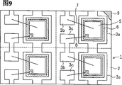
Fig. 9 is the plane graph that is illustrated in the partly cut-away of the workpiece that obtains in this traditional small size electronic unit manufacture process.The workpiece of Fig. 9 comprises a circuit board 1, have be divided into a plurality of each with the rectangle insulated substrate 2 in a corresponding zone of electronic unit.In the both sides of insulated substrate 2 each cut zone, be formed with conductive ridges part 3 (3a, 3b and 3c) and 4 (4a, 4b and 4c) with predetermined pattern.In structure shown in Figure 9, be positioned at insulated substrate 2 lip-deep conductive ridges parts 3 and comprise large scale conductive ridges part 3a and near small size conductive ridges part 3b and the 3c of a pair of part of conductive ridges dividually 3a with rectangular shape.And the conductive ridges part 4 that is positioned at insulated substrate 2 back sides comprises large scale conductive ridges part 4a and small size conductive ridges part 4b and 4c, respectively be positioned at insulated substrate 2 lip-deep conductive ridges part 3a, 3b and 3c and have approximately uniform shape.Although do not draw among the figure, be positioned at insulated substrate 2 lip-deep conductive ridges parts 3 and be positioned at the lip-deep corresponding conductive ridges part 4 of insulated substrate 2 back of the body and be electrically connected mutually through the through hole that passes insulated substrate 2 and form.
If insulated substrate 2 is made such as pottery etc. by resistant to elevated temperatures material, then conductive ridges part 3 and 4 can form by this conducting resinl of silk screen printing conducting resinl and sintering on insulated substrate 2.If insulated substrate 2 is formed from a resin, then make the surface roughening of insulated substrate 2.Then, plating catalyst is applied on this roughened surface, with electroless-plating deposit plated metal.In addition, carry out electroless-plating or have electricity to electroplate the coating that has adequate thickness with formation at the metals deposited layer.
The workpiece of electronic unit shown in Fig. 9 wherein cuts circuit board 1 with rotating blade (not drawing among the figure) along cut-off rule part (part shown in Fig. 9 dotted line) through cutting processing.Thereby the single electronic unit shown in acquisition Figure 10.
The electronic unit of the above-mentioned type for example is disclosed among the Japan Patent prospectus No.11-265964.In this electronic unit because conductive ridges part 3a, 3b and 3c and conductive ridges part 4a, 4b and 4c be positioned on the insulated substrate close to each otherly, so with compare the size that can reduce and reduce electronic unit with the electronic unit of lead frame.In addition, can make ten to hundreds of semiconductor devices simultaneously by an insulated substrate 2.
When making above-mentioned electronic unit, electronic component 5 generally is provided at large scale conductive ridges part 3a with absorption chuck (not drawing among the figure).
In addition, conducting resinl 6 is applied on the conductive ridges part 3a by the distributing method of use syringe or by method for printing screen.In distributing method, the quantity delivered of viscosity conducting resinl changes greatly.Under electronic component 5 length of sides were situation below the 0.5mm, if apply too much conducting resinl 6, then electronic component 5 was embedded in the conducting resinl 6, thereby may make partially conductive glue 6 attached on the absorption chuck.
Moreover, can be by the excessive electroconductive binder 6 that electronic component 5 is pushed open attached on adjacent conductive ridge part 3a, 3b and the 3c.If between the conductive ridge part branch of this excessive electroconductive binder 6 attached to same electronic unit, then conductive ridge part branch is short-circuited, thereby this electronic unit becomes waste product.In addition, between for example the conductive ridge part of adjacent electronic unit divided attached to different electronic units as if this excessive electroconductive binder 6, then electroconductive binder 6 exposed from potting resin part 9, as shown in Figure 11.In this case, electronic unit not only from profile or outside cut open the condition aspect and see the defectiveness that becomes, and can produce following shortcoming.That is to say, thereby might infiltrate electronic unit reduction moisture resistance by the interface between potting resin part 9 and the electroconductive binder 6 by moisture.Therefore, can be short-circuited near between the electronic unit that is provided with etc.Also may reduce the withstand voltage of electronic device, in addition, in this case, the cutting performance that is used to cut the rotating blade of electronic unit workpiece might worsen at short notice.
On the other hand, if adopt method for printing screen,, can stably apply electroconductive binder 6 with regard to the executing the amount of applying and execute and apply with regard to the position of electroconductive binder 6.
Yet in the method, when electroconductive binder being applied to simultaneously a plurality of conductive ridges part 3, electronic component 5 needs the long time be applied on the corresponding conductive ridges part 3a.The amount that is applied to the electroconductive binder 6 on each conductive ridges part 3a is greater than the amount that is applied to the electroconductive binder 6 on other each conductive ridges part 3b and the 3c.Therefore, provide the electroconductive binder 6 to each conductive ridges part 3a to flow in the past, thereby electroconductive binder 6 might arrive other conductive ridges part 3b and 3c or conductive ridges part 3a and conductive ridges part 3b and 3c near setting are short-circuited along with the time.
For fear of these shortcomings, can reduce the thickness that applies and reduce electroconductive binder 6 of executing of electroconductive binder 6.Yet after supplying with electroconductive binder 6, electroconductive binder 6 is along with time desiccation and curing in the past, and the cohesive force of electroconductive binder 6 reduces gradually.Therefore, its cohesive force has very big variation between initial electronic component of supplying with 5 and the last electronic component of supplying with 5.
Summary of the invention
Therefore, the object of the present invention is to provide a kind of circuit board, wherein electroconductive binder can be easily and is applied to promptly that conductive ridges partly goes up and stably keeps thereon, thereby electronic component can be connected to the conductive ridges part reliably.
Another object of the present invention is to provide a kind of circuit board, the electroconductive binder of scheduled volume can be applied to easily and promptly wherein that conductive ridges partly goes up and stably keep thereon, thereby electroconductive binder can not be applied to electronic component on the absorption chuck on the conductive ridges part etc. attached to being used for.
A further object of the present invention is to provide a kind of circuit board, and the electroconductive binder that wherein is supplied on the conductive ridges part can not exceed the conductive ridges part, thereby can guarantee to avoid the short circuit of conductive ridge part between grading.
A further object of the present invention is to provide a kind of circuit board, wherein is applied to electroconductive binder on the conductive ridges part and can exceed the conductive ridges part and can partly not expose from potting resin, thereby can avoid the deterioration of voltage endurance etc.
A further object of the present invention is to provide a kind of circuit board, and the electroconductive binder that wherein is supplied on the conductive ridges part can not exceed the conductive ridges part and can not be exposed to the potting resin part, thereby can avoid the rapid degeneration of cutting blade.
A further object of the present invention is to provide a kind of manufacturing to reach the method for above-mentioned purpose circuit board of the present invention.
A further object of the present invention is to provide a kind of employing to reach the electronic unit of above-mentioned purpose circuit board of the present invention.
A further object of the present invention is to eliminate the shortcoming of traditional wiring substrate and electronic unit.
According to an aspect of the present invention, provide a kind of circuit board, having comprised: insulated substrate; With the conductive ridges part, be formed on the first surface of described insulated substrate, and via electroconductive binder an electronic component be installed on it and partly be electrically connected with conductive ridges with electrode with this electronic component; The thickness that wherein centers on the conductive ridges peripheral part partly of electronic component is thicker than the thickness of this conductive ridges part middle body.
In the case, preferred described insulated substrate further has a conductive ridges part, be formed on the second surface of described insulated substrate, and partly be electrically connected with the described conductive ridges that is formed on the insulated substrate first surface via the through hole that passes insulated substrate, described second surface and first surface are opposed.
Also preferably, the conductive ridges that is formed on the insulated substrate second surface partly is used for the electronic unit that surface mount is made by this circuit board.
Further preferably, described insulated substrate has large scale conductive ridges part and at least one small size conductive ridges part that is electrically connected with this electronic component via lead of described electronic component being installed on it.
According to another aspect of the present invention, provide a kind of method of making circuit board, having comprised: prepared an insulated substrate; Photoresist film is applied on this insulated substrate, and photoresist film is formed pattern to form the part that opening portion is used to expose the insulated substrate that will form the conductive ridges part on it; Form conductive film at insulated substrate on via the opening portion exposed portions with electroless-plating; And in containing the electroplate liquid that helping the plating additive that improve to embed characteristic, there is electricity to electroplate to the insulated substrate of electroless-plating, and on the conductive film part that electroless-plating forms, is formed with the conductive film part that electricity is electroplated; Wherein there is the thickness of the peripheral part of electric plated conductive film portion to be thicker than the thickness of the conductive film of its middle body.
According to a further aspect of the invention, provide a kind of method of making circuit board, having comprised: prepared an insulated substrate; On this insulated substrate, form the conductive ridges zone; Along the thickness direction middle body in etching conductive ridge zone partly, thereby be formed on the conductive ridges part that its peripheral part has a bump.
In the case, preferably form the conductive ridges zone, comprising: on insulated substrate, form thick conductive film; Photoresist film is applied on the above thick conductive film of this insulated substrate, and photoresist film is formed pattern to expose the part that need not form the conductive ridges part of thick conductive film on the insulated substrate; And as the described thick conductive film of mask etching, and on insulated substrate, form the conductive ridges part with the photoresist film of described formation pattern; And wherein saidly be formed on the conductive ridge part branch that its peripheral part has a bump and comprise: be formed on second photoresist film that has an opening on the conductive ridges part, but the undersized of this opening is in the size of described conductive ridges part, and covers described conductive ridges peripheral part partly with this second photoresist film; And partly make this conductive ridges part be fallen by partial etching as the described conductive ridges of mask etching along thickness direction with second photoresist film.
According to a further aspect of the invention, a kind of electronic unit is provided, comprise: a circuit board, has an insulated substrate, with a conductive ridges part that is formed on this insulated substrate first surface, the thickness of described conductive ridges part peripheral part is thicker than the thickness of this conductive ridges part middle body; With an electronic component, be installed in via electroconductive binder on the middle body of described conductive ridges part, partly be electrically connected with conductive ridges with electrode this electronic component.
In the case, preferred described insulated substrate further has a conductive ridges part, is formed on the second surface of described insulated substrate, and partly is electrically connected with the described conductive ridges that is formed on the insulated substrate first surface via the through hole that passes insulated substrate.
Also the conductive ridges that preferably wherein is formed on the insulated substrate second surface partly is used for the electronic unit that surface mount is made by this circuit board.
Further preferred described insulated substrate have one its go up the large scale conductive ridges part and at least one small size conductive ridges part that is electrically connected with this electronic component via lead that described electronic component is installed.
Best described insulated substrate is partly covered by potting resin in the side that electronic component is installed.
Brief description of drawings
Can more be expressly understood these and other characteristics of the present invention and advantage from the following detailed description that provides in conjunction with the accompanying drawings, wherein identical label is represented identical or corresponding components in whole accompanying drawing, and in the accompanying drawing:
Fig. 1 represents the schematic cross sectional side views according to the electronic unit of the embodiment of the invention;
Fig. 2 is the schematic plan view of electronic unit shown in Figure 1;
Fig. 3 represents to be used in the schematic cross sectional side views of the insulated substrate in the electronic unit shown in Fig. 1 and 2;
Fig. 4 is the schematic plan view of insulated substrate shown in Figure 3;
Fig. 5 is illustrated in the schematic cross sectional side views according to circuit board workpiece in the circuit board manufacture process of the present invention;
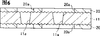
Fig. 6 is illustrated in according in the circuit board manufacture process of the present invention, obtains the schematic cross sectional side views of the workpiece of the circuit board that structure obtains afterwards shown in Fig. 5;
Fig. 7 is illustrated in according in the circuit board manufacture process of the present invention, obtains the schematic cross sectional side views of the workpiece of the circuit board that structure obtains afterwards shown in Fig. 6;
Fig. 8 is illustrated in according in the circuit board manufacture process of the present invention, obtains the schematic cross sectional side views of the workpiece of the circuit board that structure obtains afterwards shown in Fig. 7;
Fig. 9 is illustrated in the sectional plan view of the workpiece that obtains in traditional small size electronic unit manufacture process;
Figure 10 represents the profile by the conventional electronic component of the acquisition of workpiece shown in Fig. 9; And
Figure 11 represents the profile of the traditional shortcoming electronic unit that electroconductive binder wherein partly exposes from potting resin.
The explanation of preferred embodiment
With reference to accompanying drawing, describe embodiments of the invention below in detail.
Fig. 1 represents the schematic cross sectional side views according to the electronic unit 19 of the embodiment of the invention.Fig. 2 is the schematic plan view of electronic unit 19 shown in Figure 1.Fig. 3 represents to be used in the schematic cross sectional side views of the insulated substrate 11 in the electronic unit shown in Fig. 1 and 2 19.Fig. 4 is the schematic plan view of insulated substrate 11 shown in Fig. 3.
As shown in Fig. 1 and Fig. 2, electronic unit 19 generally includes circuit board 10, electronic component 14 and potting resin part 18.
And as shown in Fig. 3 and Fig. 4, circuit board 10 has insulated substrate 11, is made by for example resin.On the surface of insulated substrate 11, form conductive ridges part 12, comprise conductive ridges part 12a, 12b and 12c.On the back surface of insulated substrate 11, form conductive ridges part 13, comprise corresponding with conductive ridges part 12a, 12b and 12c respectively conductive ridges part 13a, 13b and 13c.More particularly, conductive ridges part 12 comprises large scale conductive ridges part 12a, and a pair of along conductive ridges part 12a one side setting and be positioned at small size conductive ridges part 12b and 12c near the conductive ridges part 12a.Each conductive ridges part 12a, 12b and 12c have rectangular shape in the present embodiment.And in the present embodiment, corresponding conductive ridges part 12a is electrically connected mutually via through hole 11a, the 11b and the 11c that penetrate insulated substrate 11 respectively with 13c with 13b and conductive ridges part 12c with 13a, conductive ridges part 12b.
For example, the circuit board 10 that is being used for small-size semiconductor devices, if the external dimensions of circuit board 10 is 1.0 * 1.5 * 0.25mm, then the middle body of large scale conductive ridges part 12a is decided to be 20-30 μ m, and long " a " is about 30-100 μ m at the end of bump A, and its height " h " is about 5-20 μ m.
Refer again to Fig. 1, electronic component 14 for example be semiconductor sheet part such as transistor, have the large scale main electrode 14a and the 14b that flow through principal current, be formed on the both sides of this semiconductor sheet part.Electronic component 14 also has small size control electrode 14c, and control signal applies and is used to control flowing through of principal current on it.Main electrode 14a is formed on the lower surface of electronic component 14, and main electrode 14b and control electrode 14c are formed on the upper surface of electronic component 14.Electronic component 14 is installed on the large scale conductive ridges part 12a.That is to say that the large scale main electrode 14a on electronic component 14 bottoms is connected and mechanical connection with large scale conductive ridges part 12a electronics such as silver paste etc. via electroconductive binder 15.And the main electrode 14b at electronic component 14 tops and control electrode 14c are electrically connected with small size conductive ridges part 12b and 12c via lead 16 and 17 respectively.Potting resin part 18 covers and encapsulation contains the upper surface of the circuit board 10 of electronic component 14 etc.
Can make the thickness in electronic unit 19 external dimensions be equal to or less than 0.5mm.Therefore, be suitable as can surface-pasted small size electronic unit for electronic unit 19.When the thickness of electronic unit 19 during, also must reduce the size of conductive ridges part 12a on the circuit board 10 less than 1.0mm for example.Electronic unit 19 according to the present invention has the bump A of highly about 5-20 μ m around large scale conductive ridges part 12.Therefore, can between bump A and electronic component 14, form a detention space, thereby electroconductive binder 15 can be remained in this space.Therefore, can avoid electroconductive binder 15 near and/or reach other conductive ridges parts 12b, 12c etc. on the insulated substrate 11.
As a concrete instance, suppose that large scale conductive ridges part 12a has square shape, its length of side is 750 μ m, and the bottom length of side of bump " A " is 50 μ m, and highly " h " is 10 μ m.In the case, the volume of the flat part that is centered on by bump " A " is about 4.2 * 10
6μ m
3, the volume of bump " A " is about 7 * 10
5μ m
3Therefore, the volume of bump " A " is 1/6 (about 16%) that is centered on the flat part volume by bump " A ".In the time of on electronic component 14 being installed in conductive ridges part 12a, the electroconductive binder 15 that is applied on the conductive ridges part 12a is pushed by electronic component 14, and partially conductive adhesive 15 is extruded the bottom of electronic component 14.Yet the electroconductive binder of extruding from electronic component 14 bottoms 15 can be trapped on the conductive ridges part 12a by bump A.
Even the electroconductive binder of extruding from electronic component 14 bottoms 15 exceeds bump A, also can make the amount of the electroconductive binder that exceeds bump A less.Therefore, can prevent that electroconductive binder 15 near adjacent conductive ridge part 12b, 12c etc., avoiding shortcomings such as short circuit, voltage endurance deterioration.And, can prevent that electroconductive binder 15 from exposing and avoid electronic unit 19 and other electronic units that are positioned near electronic unit 19 to be short-circuited from potting resin part 18.
The following describes the manufacture method that is used to make according to the circuit board of electronic unit of the present invention.
At first, as shown in Figure 5, preparation insulated substrate 11 is made by for example resin, and is wherein made two surperficial roughening.Then, photoresists film or photoresist film 20 are applied to the bilateral of insulated substrate 11.With photoetching technique photoresist 20 is formed predetermined pattern, thereby insulated substrate 11 is exposed at predetermined opening portion 20a.
As shown in Figure 6, the opening portion 20a place in that insulated substrate 11 exposes forms the through hole 11a that penetrates insulated substrate 11.
Although do not draw in the drawings, insulated substrate 11 is soaked in the liquid plating catalyst subsequently, and plating catalyst is applied to the through hole 11a place of opening portion 20a and insulated substrate 11.Then, this insulated substrate 11 is immersed in the electroless-plating solution, and as shown in Figure 7, forms the coating 21 of the inwall that covers each through hole 11a and opening portion 20a.
Thereby coating 21 parts on insulated substrate 11 both sides are electrically connected to each other via coating 21 parts that cover through hole 11a inwall.Then, insulated substrate 11 is immersed in the electroplating solution, and on electroless-plating layer 21, has electricity to electroplate.By will be all flat formulation (leveler) copper sulphate help the plating additive to add to be in the electric electroplating solution of having of main component, can use coating material filling vias 11a with copper sulphate, and with electric electrodeposited coating covering coating 21 parts being arranged to increase its thickness.Additive has improved the embedding characteristic of blind hole etc.The additive of the sulfuric acid of the copper sulphate of electroplating solution by mixing 160-240g/L, 40-80g/L, 30-70mg/L chloride ion, 2-10mL/L (OKUNO CHEMICAL INDUSTRIE CO., the LTD/ ProductName " TOPLUCINA BVF) and obtain.At electrolyte temperature is that 18-30 ℃ and cathode-current density are 1-5A/dm
2Condition under electroplate.
By using above-mentioned coating condition, through hole 11a is filled with coating material.In addition, coating 21 is because coating material covers also thickening.In the case, as shown in Figure 8, in each opening portion 20a, the coating material of its peripheral part is thicker than the plated material of its middle body.Therefore, when removing photoresist film 20, the peripheral part thickness that can obtain to have wherein each is thicker than the circuit board 10 of the conductive ridges part 12 of middle body.In this way, only by additive being added electroplating solution with filling vias 11a, can form wherein that peripheral part thickness is thicker than the conductive ridges part 12 of middle body, and can use insulated substrate as the circuit board that is used in the small size electronic unit with this conductive ridges part.
In the method for above-mentioned manufacturing circuit board 10, electrodeposited coating 21 is formed on the bilateral of insulated substrate 11, and with the coating material of filling vias 11a these electrodeposited coatings 21 is electrically connected mutually.Yet, can also a side form electrodeposited coating 21 at insulated substrate 11.In the case, needn't form the through hole that resembles the through hole 11a.
The present invention is not limited to said structure and method.For example, can make with other modes according to circuit board of the present invention.That is to say, can be film plated with photoresist be formed with enough insulated substrates of thick electrodeposited coating on it.Photoresist film is formed pattern must make predetermined portions be removed.The removal partial etching of photoresist film is fallen, have the conductive ridges part of predetermined pattern thereby form.Then, form another photoresist film and form pattern and make this photoresist film on conductive ridges part, have opening.The undersized of individual opening is in the opening size of corresponding conductive ridges part, and film covers conductive ridges peripheral part partly with photoresist.By with this photoresist film as mask, conductive ridges partly etched away make its middle body be thinner than peripheral part.Thereby, can be formed on the conductive ridges part that its periphery has bump.
As mentioned above, in circuit board according to the present invention, the peripheral part thickness that the conductive ridges part of electronic component is installed on it is thicker than the thickness of its middle body.Therefore, when promptly using method for printing screen etc. that electroconductive binder is applied to many conductive ridges simultaneously and partly goes up, becoming to prevent that the viscosity electroconductive binder from flowing out the conductive ridges part, and the electroconductive binder of scheduled volume stably can be trapped on each conductive ridges part.
Can also prevent that electroconductive binder is provided to absorption chuck on the conductive ridges part to electronic component attached to being used for.
In addition, can prevent that excessive electroconductive binder from arriving the adjacent conductive ridge part and partly expose from potting resin.Thereby, can guarantee to avoid the short circuit between the conductive ridge part branch, the deterioration of voltage endurance etc.
And, with cutting blade cutting potting resin part the time, can avoid the rapid degeneration of cutting blade.
In above stated specification, describe the present invention with reference to specific embodiment.Yet, it should be understood by one skilled in the art that and can make multiple remodeling and variation and do not depart from by the given scope of the present invention of following claim.Therefore, will be understood that explanation and diagram are exemplary and nonrestrictive, and all these remodeling all should be within the scope of the present invention.Therefore, the invention is intended to contain all changes and the remodeling that falls in the claims scope.
Claims (12)
1. circuit board comprises:
Insulated substrate; With
The conductive ridges part is formed on the first surface of described insulated substrate, and via electroconductive binder electronic component is installed on it and partly is electrically connected with conductive ridges with the electrode with this electronic component;
Wherein conductive ridges partly is thicker than the thickness of this conductive ridges part middle body around the thickness of the peripheral part of electronic component.
2. circuit board as claimed in claim 1, wherein said insulated substrate further has a conductive ridges part, be formed on the second surface of described insulated substrate, and partly be electrically connected with the described conductive ridges that is formed on the insulated substrate first surface via the through hole that passes insulated substrate, described second surface is mutually opposed with first surface.
3. circuit board as claimed in claim 2, the conductive ridges that wherein is formed on the insulated substrate second surface partly is used for and will carries out surface mount by the electronic unit of this circuit board making.
4. circuit board as claimed in claim 1, wherein said insulated substrate have one the large scale conductive ridges part of described electronic component and small size conductive ridges part that at least one is electrically connected with this electronic component via lead or wiring are installed on it.
5. method of making circuit board comprises:
The preparation insulated substrate;
Photoresist film is applied on this insulated substrate, and photoresist film is formed pattern to form opening portion, be used to expose the part of the insulated substrate that will form the conductive ridges part on it;
Form conductive film at insulated substrate on via the opening portion exposed portions with electroless-plating; And
Contain help the plating additive with the electroplate liquid that improve to embed characteristic in, have electricity to electroplate to the insulated substrate through electroless-plating, and on the conductive film part that electroless-plating forms, be formed with the conductive film part that electricity is electroplated;
Wherein there is the thickness of the peripheral part of electric plated conductive film portion to be thicker than the thickness of its middle body.
6. method of making circuit board comprises:
The preparation insulated substrate;
On this insulated substrate, form the conductive ridges zone;
Along the middle body in thickness direction partial etching conductive ridges zone, thereby be formed on the conductive ridges part that its peripheral part has bump.
7. circuit board manufacture method as claimed in claim 6 wherein forms the conductive ridges zone and comprises:
On insulated substrate, form thick conductive film;
Photoresist film is applied on the described thick conductive film on this insulated substrate, and photoresist film is formed pattern to expose the part that does not form the conductive ridges part of thick conductive film on the insulated substrate; And
Photoresist film with described formation pattern forms the conductive ridges part as the described thick conductive film of mask etching and on insulated substrate; And
Wherein saidly be formed on the conductive ridge part branch that its peripheral part has bump and comprise:
Be formed on second photoresist film that has opening on the conductive ridges part, but the undersized of this opening and covers described conductive ridges peripheral part partly with this second photoresist film in the size of described conductive ridges part; And
As the described conductive ridges part of mask etching, make this conductive ridges part be fallen by partial etching with second photoresist film along thickness direction.
8. electronic unit comprises:
Circuit board has insulated substrate and is formed on conductive ridges part on this insulated substrate first surface, and the thickness of described conductive ridges part peripheral part is thicker than the thickness of this conductive ridges part middle body; With
Electronic component is installed in via electroconductive binder on the middle body of described conductive ridges part and partly is electrically connected with conductive ridges with the electrode with this electronic component.
9. electronic unit as claimed in claim 8, wherein said insulated substrate further has the conductive ridges part, be formed on the second surface of described insulated substrate, and partly be electrically connected with the described conductive ridges that is formed on the insulated substrate first surface via the through hole that passes insulated substrate, described second surface is mutually opposed with first surface.
10. electronic unit as claimed in claim 9, the conductive ridges that wherein is formed on the insulated substrate second surface partly is used for and will carries out surface mount by the electronic unit of this circuit board making.
11. electronic unit as claimed in claim 8, wherein said insulated substrate have large scale conductive ridges part that described electronic component is installed on it and the small size conductive ridges part that at least one is electrically connected with this electronic component via lead or wiring.
12. electronic unit as claimed in claim 8, wherein said insulated substrate is partly covered by a potting resin in the side that electronic component is installed.
Applications Claiming Priority (2)
| Application Number | Priority Date | Filing Date | Title |
|---|---|---|---|
| JP290695/2001 | 2001-09-25 | ||
| JP2001290695A JP2003101204A (en) | 2001-09-25 | 2001-09-25 | Wiring substrate, method of manufacturing the same, and electronic component |
Publications (1)
| Publication Number | Publication Date |
|---|---|
| CN1411055A true CN1411055A (en) | 2003-04-16 |
Family
ID=19112964
Family Applications (1)
| Application Number | Title | Priority Date | Filing Date |
|---|---|---|---|
| CN02143438A Pending CN1411055A (en) | 2001-09-25 | 2002-09-25 | Wiring substrate for small electronic unit and mfg. method thereof |
Country Status (5)
| Country | Link |
|---|---|
| US (1) | US20030058629A1 (en) |
| JP (1) | JP2003101204A (en) |
| KR (1) | KR20030026855A (en) |
| CN (1) | CN1411055A (en) |
| TW (1) | TW560234B (en) |
Cited By (3)
| Publication number | Priority date | Publication date | Assignee | Title |
|---|---|---|---|---|
| CN103247578A (en) * | 2012-02-01 | 2013-08-14 | 矽品精密工业股份有限公司 | Semiconductor carrier and package and fabrication method thereof |
| CN105247971A (en) * | 2013-05-24 | 2016-01-13 | 诺基亚技术有限公司 | Substrates for electronic components, associated methods and apparatus |
| WO2021097614A1 (en) * | 2019-11-18 | 2021-05-27 | 苏州新光维医疗科技有限公司 | Integrated miniature welding plate structure and manufacturing process therefor |
Families Citing this family (45)
| Publication number | Priority date | Publication date | Assignee | Title |
|---|---|---|---|---|
| TWI338132B (en) * | 2003-03-25 | 2011-03-01 | Toppan Printing Co Ltd | Analytic method for plating liquid for eletrolyzing copper and method for manufacturing a semiconductor product |
| JP5039908B2 (en) * | 2005-10-17 | 2012-10-03 | セイコーインスツル株式会社 | Manufacturing method of semiconductor device |
| TWI270187B (en) * | 2005-12-19 | 2007-01-01 | Polytronics Technology Corp | Thermal conductive apparatus and manufacturing method thereof |
| CN100596255C (en) * | 2006-08-11 | 2010-03-24 | 高陆股份有限公司 | Method for manufacturing high-wattage fine line carrier and structure thereof |
| JP5010208B2 (en) * | 2006-08-17 | 2012-08-29 | 三菱重工業株式会社 | Semiconductor element module and manufacturing method thereof |
| US20090181390A1 (en) * | 2008-01-11 | 2009-07-16 | Signosis, Inc. A California Corporation | High throughput detection of micrornas and use for disease diagnosis |
| US10072287B2 (en) | 2009-09-10 | 2018-09-11 | Centrillion Technology Holdings Corporation | Methods of targeted sequencing |
| US10174368B2 (en) | 2009-09-10 | 2019-01-08 | Centrillion Technology Holdings Corporation | Methods and systems for sequencing long nucleic acids |
| AU2010315084A1 (en) | 2009-11-06 | 2012-05-31 | The Board Of Trustees Of The Leland Stanford Junior University | Non-invasive diagnosis of graft rejection in organ transplant patients |
| DE102010044709B4 (en) * | 2010-09-08 | 2015-07-02 | Vincotech Holdings S.à.r.l. | Power semiconductor module with metal sintered connections and manufacturing process |
| CN103703143B (en) | 2011-01-31 | 2016-12-14 | 爱普瑞斯生物公司 | The method of the multiple epi-positions in identification of cell |
| US20120252682A1 (en) | 2011-04-01 | 2012-10-04 | Maples Corporate Services Limited | Methods and systems for sequencing nucleic acids |
| EP2776962A4 (en) | 2011-11-07 | 2015-12-02 | Ingenuity Systems Inc | Methods and systems for identification of causal genomic variants |
| US10174310B2 (en) | 2012-08-08 | 2019-01-08 | Roche Sequencing Solutions, Inc. | Increasing dynamic range for identifying multiple epitopes in cells |
| US20160040234A1 (en) | 2013-03-15 | 2016-02-11 | Lineage Biosciences, Inc. | Methods of sequencing the immune repertoire |
| WO2014151117A1 (en) | 2013-03-15 | 2014-09-25 | The Board Of Trustees Of The Leland Stanford Junior University | Identification and use of circulating nucleic acid tumor markers |
| CN111593414A (en) | 2013-08-05 | 2020-08-28 | 特韦斯特生物科学公司 | De novo synthetic gene library |
| JP7451070B2 (en) | 2013-11-07 | 2024-03-18 | ザ ボード オブ トラスティーズ オブ ザ レランド スタンフォード ジュニア ユニバーシティー | Cell-free nucleic acids for analysis of the human microbiome and its components |
| WO2016126882A1 (en) | 2015-02-04 | 2016-08-11 | Twist Bioscience Corporation | Methods and devices for de novo oligonucleic acid assembly |
| WO2016126987A1 (en) | 2015-02-04 | 2016-08-11 | Twist Bioscience Corporation | Compositions and methods for synthetic gene assembly |
| WO2016172377A1 (en) | 2015-04-21 | 2016-10-27 | Twist Bioscience Corporation | Devices and methods for oligonucleic acid library synthesis |
| IL258164B (en) | 2015-09-18 | 2022-09-01 | Twist Bioscience Corp | Methods to regulate the activity of proteins and cells and a method for the production of nucleic acids |
| US11512347B2 (en) | 2015-09-22 | 2022-11-29 | Twist Bioscience Corporation | Flexible substrates for nucleic acid synthesis |
| EP3384077A4 (en) | 2015-12-01 | 2019-05-08 | Twist Bioscience Corporation | Functionalized surfaces and preparation thereof |
| CN116987777A (en) | 2016-03-25 | 2023-11-03 | 凯锐思公司 | Synthesis of nucleic acid inclusions |
| SG11201901563UA (en) | 2016-08-22 | 2019-03-28 | Twist Bioscience Corp | De novo synthesized nucleic acid libraries |
| EP3516528A4 (en) | 2016-09-21 | 2020-06-24 | Twist Bioscience Corporation | Nucleic acid based data storage |
| US10907274B2 (en) | 2016-12-16 | 2021-02-02 | Twist Bioscience Corporation | Variant libraries of the immunological synapse and synthesis thereof |
| US11550939B2 (en) | 2017-02-22 | 2023-01-10 | Twist Bioscience Corporation | Nucleic acid based data storage using enzymatic bioencryption |
| AU2018234629A1 (en) | 2017-03-15 | 2019-10-17 | Twist Bioscience Corporation | Variant libraries of the immunological synapse and synthesis thereof |
| EP3610034B1 (en) | 2017-04-12 | 2022-06-08 | Karius, Inc. | Sample preparation methods, systems and compositions |
| WO2018231864A1 (en) | 2017-06-12 | 2018-12-20 | Twist Bioscience Corporation | Methods for seamless nucleic acid assembly |
| KR20240013290A (en) | 2017-06-12 | 2024-01-30 | 트위스트 바이오사이언스 코포레이션 | Methods for seamless nucleic acid assembly |
| GB2581620A (en) | 2017-09-11 | 2020-08-26 | Twist Bioscience Corp | GPCR binding proteins and synthesis thereof |
| WO2019060716A1 (en) | 2017-09-25 | 2019-03-28 | Freenome Holdings, Inc. | Methods and systems for sample extraction |
| CA3079613A1 (en) | 2017-10-20 | 2019-04-25 | Twist Bioscience Corporation | Heated nanowells for polynucleotide synthesis |
| US10936953B2 (en) | 2018-01-04 | 2021-03-02 | Twist Bioscience Corporation | DNA-based digital information storage with sidewall electrodes |
| KR20210013128A (en) | 2018-05-18 | 2021-02-03 | 트위스트 바이오사이언스 코포레이션 | Polynucleotides, reagents and methods for nucleic acid hybridization |
| US11492727B2 (en) | 2019-02-26 | 2022-11-08 | Twist Bioscience Corporation | Variant nucleic acid libraries for GLP1 receptor |
| US11492728B2 (en) | 2019-02-26 | 2022-11-08 | Twist Bioscience Corporation | Variant nucleic acid libraries for antibody optimization |
| CN114729342A (en) | 2019-06-21 | 2022-07-08 | 特韦斯特生物科学公司 | Barcode-Based Nucleic Acid Sequence Assembly |
| EP4464827A3 (en) | 2019-09-23 | 2025-02-26 | Twist Bioscience Corporation | Variant nucleic acid libraries for crth2 |
| US12173282B2 (en) | 2019-09-23 | 2024-12-24 | Twist Bioscience, Inc. | Antibodies that bind CD3 epsilon |
| WO2024123733A1 (en) | 2022-12-05 | 2024-06-13 | Twist Bioscience Corporation | Enzymes for library preparation |
| WO2024220475A1 (en) | 2023-04-21 | 2024-10-24 | Twist Bioscience Corporation | Polymerase variants |
Family Cites Families (7)
| Publication number | Priority date | Publication date | Assignee | Title |
|---|---|---|---|---|
| JPH08255969A (en) * | 1995-03-17 | 1996-10-01 | Sony Corp | Printed-circuit board device |
| KR100331072B1 (en) * | 1998-05-27 | 2003-12-31 | 앰코 테크놀로지 코리아 주식회사 | Printed circuit board |
| JP3764587B2 (en) * | 1998-06-30 | 2006-04-12 | 富士通株式会社 | Manufacturing method of semiconductor device |
| JP2000124587A (en) * | 1998-10-19 | 2000-04-28 | Alps Electric Co Ltd | Fitting method and fitting structure of electronic circuit unit to printed board |
| EP1055192A1 (en) * | 1998-12-18 | 2000-11-29 | Koninklijke Philips Electronics N.V. | Data carrier module with integrated circuit and transmission coil |
| KR100327705B1 (en) * | 1999-07-15 | 2002-03-08 | 전우창 | Method of producing a multi-layer printed-circuit board |
| JP2002231882A (en) * | 2001-02-06 | 2002-08-16 | Mitsubishi Electric Corp | Semiconductor device |
-
2001
- 2001-09-25 JP JP2001290695A patent/JP2003101204A/en active Pending
-
2002
- 2002-09-17 KR KR1020020056450A patent/KR20030026855A/en not_active Application Discontinuation
- 2002-09-24 TW TW091121947A patent/TW560234B/en active
- 2002-09-24 US US10/253,295 patent/US20030058629A1/en not_active Abandoned
- 2002-09-25 CN CN02143438A patent/CN1411055A/en active Pending
Cited By (6)
| Publication number | Priority date | Publication date | Assignee | Title |
|---|---|---|---|---|
| CN103247578A (en) * | 2012-02-01 | 2013-08-14 | 矽品精密工业股份有限公司 | Semiconductor carrier and package and fabrication method thereof |
| CN103247578B (en) * | 2012-02-01 | 2015-12-16 | 矽品精密工业股份有限公司 | Semiconductor carrier and package and fabrication method thereof |
| CN105247971A (en) * | 2013-05-24 | 2016-01-13 | 诺基亚技术有限公司 | Substrates for electronic components, associated methods and apparatus |
| CN105247971B (en) * | 2013-05-24 | 2018-06-26 | 诺基亚技术有限公司 | Substrate, associated method and apparatus for electronic unit |
| WO2021097614A1 (en) * | 2019-11-18 | 2021-05-27 | 苏州新光维医疗科技有限公司 | Integrated miniature welding plate structure and manufacturing process therefor |
| GB2604516A (en) * | 2019-11-18 | 2022-09-07 | Scivita Med Tech Co Ltd | Integrated miniature welding plate structure and manufacturing process therefor |
Also Published As
| Publication number | Publication date |
|---|---|
| JP2003101204A (en) | 2003-04-04 |
| TW560234B (en) | 2003-11-01 |
| KR20030026855A (en) | 2003-04-03 |
| US20030058629A1 (en) | 2003-03-27 |
Similar Documents
| Publication | Publication Date | Title |
|---|---|---|
| CN1411055A (en) | Wiring substrate for small electronic unit and mfg. method thereof | |
| CN1225783C (en) | Semiconductor component basement and manufacture thereof, semiconductor potted element | |
| CN1178243C (en) | capacitor | |
| CN1298034C (en) | Semiconductor package having semiconductor constructing body and method of manufacturing the same | |
| CN1264214C (en) | Electronic package having embedded capacitors and method of fabrication therefor | |
| CN1309281C (en) | Circuit board and method for manufacturing the same | |
| CN1946271A (en) | Printed circuit board and manufacturing method thereof | |
| CN1479330A (en) | Solid electrolytic capacitor and manufacturing method thereof | |
| CN1658387A (en) | Semiconductor device and manufacturing method thereof | |
| CN101066004A (en) | Method for manufacturing substrate having via hole filled with conductive material | |
| CN1489429A (en) | Method for manufacturing circuit board and communication device | |
| CN1717964A (en) | Electronic component and its manufacturing method | |
| CN1666327A (en) | Flexible wiring base material and process for producing the same | |
| CN1762185A (en) | Process for producing electronic component and electronic component | |
| CN1341963A (en) | Semiconductor device and manufacturing method thereof | |
| CN1489202A (en) | Electronic device module | |
| CN1369912A (en) | Semiconductor integrated circuit and its preparing method | |
| CN1161010C (en) | Method for producing wiring between upper and lower sides of substrate with conductive interconnection and wiring with the interconnection on substrate | |
| CN1993021A (en) | Method for manufacturing wiring board | |
| CN1509134A (en) | Method for producing circuit device, circuit moudle and method for producing circuit devicd | |
| CN1301542C (en) | Semiconductor wafer, semiconductor device and its producing method, circuit base board and electronic machine | |
| CN1465079A (en) | Circuit breaker for low-voltage currents | |
| CN100350525C (en) | Manufacturing method for solid electrolytic capacitor | |
| CN1689382A (en) | Multilayer printed wiring board and production method therefor | |
| CN1306856C (en) | Electroplating method of prited circuit board |
Legal Events
| Date | Code | Title | Description |
|---|---|---|---|
| C06 | Publication | ||
| PB01 | Publication | ||
| ASS | Succession or assignment of patent right |
Owner name: NEC ELECTRONICS TAIWAN LTD. Free format text: FORMER OWNER: NIPPON ELECTRIC CO., LTD. Effective date: 20030408 |
|
| C41 | Transfer of patent application or patent right or utility model | ||
| TA01 | Transfer of patent application right |
Effective date of registration: 20030408 Applicant after: NEC Corp. Applicant before: NEC Corp. |
|
| C10 | Entry into substantive examination | ||
| SE01 | Entry into force of request for substantive examination | ||
| C02 | Deemed withdrawal of patent application after publication (patent law 2001) | ||
| WD01 | Invention patent application deemed withdrawn after publication |