CN1389987A - Analogue quadrature moducator error compensating apparatus and method - Google Patents
Analogue quadrature moducator error compensating apparatus and method Download PDFInfo
- Publication number
- CN1389987A CN1389987A CN02122146.4A CN02122146A CN1389987A CN 1389987 A CN1389987 A CN 1389987A CN 02122146 A CN02122146 A CN 02122146A CN 1389987 A CN1389987 A CN 1389987A
- Authority
- CN
- China
- Prior art keywords
- signal
- digital signal
- feedback
- digital
- error
- Prior art date
- Legal status (The legal status is an assumption and is not a legal conclusion. Google has not performed a legal analysis and makes no representation as to the accuracy of the status listed.)
- Pending
Links
Images


Classifications
-
- H—ELECTRICITY
- H04—ELECTRIC COMMUNICATION TECHNIQUE
- H04L—TRANSMISSION OF DIGITAL INFORMATION, e.g. TELEGRAPHIC COMMUNICATION
- H04L27/00—Modulated-carrier systems
- H04L27/32—Carrier systems characterised by combinations of two or more of the types covered by groups H04L27/02, H04L27/10, H04L27/18 or H04L27/26
- H04L27/34—Amplitude- and phase-modulated carrier systems, e.g. quadrature-amplitude modulated carrier systems
- H04L27/36—Modulator circuits; Transmitter circuits
- H04L27/366—Arrangements for compensating undesirable properties of the transmission path between the modulator and the demodulator
- H04L27/367—Arrangements for compensating undesirable properties of the transmission path between the modulator and the demodulator using predistortion
- H04L27/368—Arrangements for compensating undesirable properties of the transmission path between the modulator and the demodulator using predistortion adaptive predistortion
Landscapes
- Engineering & Computer Science (AREA)
- Computer Networks & Wireless Communication (AREA)
- Signal Processing (AREA)
- Amplifiers (AREA)
Abstract
一种AQM误差补偿装置,包括:预失真器,用于使信号失真,从而具有和数字输入信号的非线性失真特性相反的特性;误差补偿单元,用于根据误差校正信号来补偿从预失真器输出的I/Q数字信号;数/模转换器,用于把误差补偿单元的I/Q数字信号转换为I/Q模拟信号;调制器,用于对从数/模转换器输出的I/Q模拟信号进行频率调制;功率放大器,用于放大调制器的输出信号,并提供给定向耦合器;下变频器,用于对从定向耦合器输入的反馈信号进行下变频;模/数转换器,用于把下变频器的输出信号转换为数字信号;以及控制器,用于对模/数转换器的输出信号和从预失真器输入的I/Q数字信号进行比较,并向误差补偿单元施加所提取的误差校正信号。
An AQM error compensation device, comprising: a predistorter for distorting a signal so as to have a characteristic opposite to the non-linear distortion characteristic of a digital input signal; an error compensation unit for compensating from the predistorter according to an error correction signal The output I/Q digital signal; the digital/analog converter, which is used to convert the I/Q digital signal of the error compensation unit into an I/Q analog signal; the modulator, which is used to output the I/Q signal from the digital/analog converter. Q analog signal for frequency modulation; power amplifier for amplifying the output signal of the modulator and providing it to the directional coupler; downconverter for downconverting the feedback signal input from the directional coupler; analog/digital converter , for converting the output signal of the down-converter into a digital signal; and a controller, for comparing the output signal of the analog/digital converter with the I/Q digital signal input from the predistorter, and sending the signal to the error compensation unit The extracted error correction signal is applied.
Description
技术领域technical field
本发明涉及模拟正交调制器(AQM)误差补偿装置及方法,特别涉及用于消除关于探测器的非线性特性和热噪声的AQM误差的AQM误差补偿装置及方法。The present invention relates to an analog quadrature modulator (AQM) error compensation device and method, in particular to an AQM error compensation device and method for eliminating AQM errors related to detector nonlinear characteristics and thermal noise.
背景技术Background technique
通常,功率放大器放大输入的射频信号,在这点上,功率放大器只是线性地放大信号的强度,而不使信号失真。Typically, a power amplifier amplifies an incoming radio frequency signal, and at this point, the power amplifier only linearly amplifies the strength of the signal without distorting the signal.
但是,因为每个功率放大器都包含多个具有非线性特性的有源器件,所以包括功率放大器的整体系统的性能受到负面影响。However, because each power amplifier contains multiple active devices with non-linear characteristics, the performance of the overall system including the power amplifier is negatively affected.
作为改善功率放大器的非线性特性的方法,有前馈法、包络反馈(envelope feedback)法、预失真法、偏置补偿(bias compensation)法,等等。As a method of improving the nonlinear characteristics of a power amplifier, there are a feedforward method, an envelope feedback method, a predistortion method, a bias compensation method, and the like.
目前,在线性化的方法中,预失真法得到了广泛的应用,因为对于其性能它的价格最低,而且可以在更宽的带宽中工作。Currently, among the linearization methods, the predistortion method is widely used because it is the cheapest for its performance and can work in a wider bandwidth.
预失真法提高了系统的线性度,将输入信号预失真为具有与非线性失真特性相反的特性,然后输入到功率放大器中。因为预失真法可以在基带中实现,所以整体系统的尺寸和效率都得到了改善。The predistortion method improves the linearity of the system, predistorts the input signal to have characteristics opposite to the nonlinear distortion characteristics, and then inputs it into the power amplifier. Because the predistortion method can be implemented in baseband, the size and efficiency of the overall system are improved.
另外,为了实现具有更宽带宽的预失真系统,利用AQM,而不是数字正交调制器(DQM)来实现整体系统。In addition, in order to realize a predistortion system with a wider bandwidth, the overall system is realized using AQM instead of a digital quadrature modulator (DQM).
但是,因为AQM包括模拟装置,所以它具有误差成分,比如DC偏移或者幅/相失衡,这是降低预失真器的性能的主要因素。这样,为了得到最好的预失真器性能,应该补偿AQM误差。However, since AQM includes analog devices, it has error components, such as DC offset or amplitude/phase imbalance, which are major factors that degrade the performance of the predistorter. Thus, for best predistorter performance, AQM errors should be compensated.
图1是显示模拟正交调制器(AQM)误差补偿装置的方框图。FIG. 1 is a block diagram showing an analog quadrature modulator (AQM) error compensation device.
如图1所示,由预失真器110到定向耦合器5的路径是主路径,而由定向耦合器5到控制器9的路径是反馈路径,用以检测主要由AQM产生的误差成分。这时,在AQM中由于DC偏移、增益和相位失衡而产生误差成分。As shown in FIG. 1 , the path from the
传统的模拟正交调制器误差补偿装置包括:预失真器110,用于对通过调制解调器1输入的数字信号进行预失真,以抵消非线性特性;误差补偿单元120,用于根据误差校正信号来补偿从预失真器110输出的数字信号;数-模转换器10,用于把从误差补偿单元120输出的数字信号转换为模拟信号;调制器20,用于把从数-模转换器10输出的模拟信号调制为载波频率;功率放大器4,用于放大调制器20的输出信号,并把它施加到定向耦合器5;放大器6,用于把从定向耦合器5输入的反馈信号放大到一定的电平;检测器7,用于测量从放大器6输出的信号的DC平均值;模-数转换器8,用于把从检测器7输出的DC平均值转换为数字信号;以及控制器9,用于通过模-数转换器8的输出信号检测误差,并输出误差校正信号以补偿该误差。The traditional analog quadrature modulator error compensation device includes: a
误差补偿单元120实现调制器20的等效电路,预失真器110使数字输入信号失真,以具有功率放大器4的非线性失真特性的相反特性,并把数字输入信号分离为I/Q数字信号(Id,Qd)并输出它们。The
误差补偿单元120包括:第一放大器121,用于控制已经根据控制器9发出的第一增益校正信号(α)预失真的I数字信号(Id)的增益;第二放大器122,用于控制已经根据控制器9发出的第二增益校正信号(β)预失真的Q数字信号(Qd)的增益;第三放大器123,用于根据第一相位校正信号(sinφ)控制第二放大器122的输出信号的相位;第四放大器125,用于根据第二相位校正信号(cosφ)控制第二放大器122的输出信号的相位;第一加法器124,用于把第一放大器121的输出和第三放大器123的输出相加;第二加法器126,用于把第一加法器124的输出信号和第一DC偏移信号(C1)相加;以及第三加法器127,用于把第四放大器125的输出信号和第二DC偏移信号(C2)相加。The
数-模转换器10包括:第一数/模转换器11,用于接收从误差补偿单元120输出的I数字信号,并将其转换为I模拟信号;以及第二数/模转换器12,用于接收从误差补偿单元120输出的Q数字信号,并将其转换为Q模拟信号。The digital-to-
调制器20包括:第一乘法器21,用于把从第一数/模转换器11输出的I模拟信号和从本机振荡器(LO)输出的本机震荡频率信号相乘;第二乘法器22,用于把从第二数/模转换器12输出的Q模拟信号和从本机荡器(LO)输出的本机震荡频率信号相乘;以及合成器23,用于把第一和第二乘法器21和22的输出信号合成,并输出射频信号。The
现在说明如上所述构成的普通AQM误差补偿装置的操作。The operation of the conventional AQM error compensating apparatus constructed as described above will now be described.
首先,预失真器110对通过调制解调器1输入的数字信号进行预失真,以具有与功率放大器4的非线性失真特性相反的特性,并输出I数字信号(Id)和Q数字信号(Qd)。First, the
误差补偿单元120校正从预失真器110输出的I/Q数字信号(Id,Qd)的误差,把它们施加到第一和第二数/模转换器11和12。The
然后,第一和第二数/模转换器11和12把输入的I/Q数字信号转换为I/Q模拟信号并输出它们。Then, the first and second D/
也就是说,第一数/模转换器11接收I数字信号并将其转换为I模拟信号,而第二数/模转换器12接收Q数字信号并将其转换为Q模拟信号。That is, the first D/
调制器20接收从第一和第二数/模转换器11和12输出的I/Q模拟信号,并对其进行AQM调制。The
也就是说,在调制器20中,第一乘法器21把从第一数/模转换器11输出的I模拟信号和从本机振荡器输出的本机震荡频率信号相乘,以进行上变频,而第二乘法器22把从第二数/模转换器12输出的Q模拟信号和从本机振荡器输出的本机震荡频率信号相乘,以进行上变频。That is, in the
每个上变频信号都被合成器23合成为射频信号,并被施加到功率放大器4。Each up-converted signal is synthesized into a radio frequency signal by the synthesizer 23 and applied to the
放大器6通过功率放大器4将从定向耦合器5输入的反馈信号放大至一定的电平,检测器7测量从放大器6输出的信号的DC平均值,并将其输出到模/数转换器8。
模/数转换器8将从检测器7输出的DC平均值转换为数字信号,并将其施加到控制器9,控制器9通过转换并输出后的信号测量误差,并把用于补偿误差值的误差校正信号施加到误差补偿单元120中。The analog-to-
这时,误差校正信号包括:第一和第二DC偏移信号(C1,C2),用于校正I/Q数字信号的DC偏移;第一和第二增益校正信号(α和β),用于校正I/Q数字信号的增益误差;以及相位校正信号(),用于校正I/Q数字信号的相位误差。At this time, the error correction signal includes: first and second DC offset signals (C1, C2), used to correct the DC offset of the I/Q digital signal; first and second gain correction signals (α and β), used to correct the gain error of the I/Q digital signal; and a phase correction signal (), used to correct the phase error of the I/Q digital signal.
现在参照图2、3和4说明确定误差校正信号的过程。The process of determining the error correction signal will now be described with reference to FIGS. 2, 3 and 4. FIG.
图2是显示用于确定DC偏移的第一和第二DC偏移信号过程的图。FIG. 2 is a diagram showing a first and second DC offset signal process for determining a DC offset.
如图2所示,控制器9把测试向量设置为‘0’,并初始化误差校正装置的增益失衡、相位失衡和DC偏移失衡值(步骤S11),固定Q信道的DC偏移信号(C2),变化I信道的DC偏移信号(C1)(步骤S12)。As shown in Figure 2, the
这时,控制器9检测输出到检测器7的信号,并把输出信号最小的时间点确定为第一DC偏移信号(C1),即I信道DC偏移信号(步骤S13、S14)。At this time, the
关于第二DC偏移信号(C2),第二DC偏移信号(C2)固定I信道的DC偏移信号(C1)之后,变化Q信道的DC偏移信号(C2)(步骤S15),以检测输出到检测器7的信号,并把输出信号最小的时间点确定为Q信道DC偏移信号(C2)(步骤S17)。Regarding the second DC offset signal (C2), after the second DC offset signal (C2) fixes the DC offset signal (C1) of the I channel, the DC offset signal (C2) of the Q channel is changed (step S15) to The signal output to the
图3是显示确定增益校正信号过程的图。FIG. 3 is a diagram showing a process of determining a gain correction signal.
如图3所示,控制器9施加具有I信道信号‘A’和Q信道信号‘0’的测试向量(步骤S21),以检测从检测器7输出的第一输出信号(步骤S22),并施加具有I信道信号‘0’和特定值‘A’的Q信道信号的测试向量(步骤S23),以检测从检测器7输出的第二输出信号(步骤S24),然后,控制器确定第一输出信号除以第二输出信号所得的值是否近似于1(步骤S25)。As shown in FIG. 3, the
如果第一输出信号除以第二输出信号所得的值大于1,而不是约等于1(步骤S26),则控制器9把第二增益校正信号(β)固定为‘1’,然后把第一增益校正信号(α)变化为小于‘1’。If the value obtained by dividing the first output signal by the second output signal is greater than 1, rather than approximately equal to 1 (step S26), the
但是,如果第一输出信号除以第二输出信号所得的值小于1,则控制器9把第一增益校正信号(α)固定为‘1’,然后把第二增益校正信号(β)变化为小于‘1’(步骤S28),从而确定了第一和第二增益校正信号(α和β)(步骤S29)。However, if the value obtained by dividing the first output signal by the second output signal is less than 1, the
图4是显示用于确定相位校正信号过程的图。FIG. 4 is a diagram showing a process for determining a phase correction signal.
如图4所示,控制器9向I信道和Q信道施加某一测试向量(A,A) (步骤S31)以检测来自检测器7的第一输出信号(步骤S32),并向I信道和Q信道施加某一测试向量(-A,A)(步骤S33)以检测来自检测器7的第二输出信号(步骤S34),并确定第一和第二输出信号的大小以得到大小比率(Er)(步骤S35)。As shown in Figure 4, the
对于大小比率(Er),如果第一输出信号大于第二输出信号,则确定I和Q信号之间存在小于90度的差异,并把第一输出信号除以第二输出信号所得的值作为大小比率(Er)进行检测(步骤S36)。For the magnitude ratio (Er), if the first output signal is greater than the second output signal, determine that there is less than a 90 degree difference between the I and Q signals, and divide the first output signal by the second output signal as the magnitude The ratio (Er) is detected (step S36).
但是,如果第一输出信号小于第二输出信号,则确定I和Q信号之间存在大于90度的差异,并把第二输出信号除以第一输出信号的值作为大小比率(Er)进行检测(步骤S37)。
把第一和第二输出信号的大小比率代入公式(1)进行计算(步骤S38),从而检测到相位校正信号(φ),由此得到第一相位校正信号(sinφ)和第二相位校正信号(cosφ)(步骤S39)。Substituting the size ratio of the first and second output signals into formula (1) for calculation (step S38), thereby detecting the phase correction signal (φ), thus obtaining the first phase correction signal (sinφ) and the second phase correction signal (cos?) (step S39).
如上所述,在传统的AQM误差校正装置中,为了提取AQM误差,控制器施加测试向量,由因为所得到的DC偏移引起的误差、增益和由该相位失衡引起的相位失衡计算AQM误差补偿值,并预先设置对应于该误差补偿值的误差校正信号。As mentioned above, in the conventional AQM error correction device, in order to extract the AQM error, the controller applies the test vector, calculates the AQM error compensation from the error due to the resulting DC offset, the gain, and the phase imbalance caused by this phase imbalance value, and preset the error correction signal corresponding to the error compensation value.
由此,传统的AQM误差校正装置具有以下的问题。Thus, the conventional AQM error correction device has the following problems.
即,因为即使由输入信号产生的误差变化了,也无法调整预先设置在误差补偿单元中的误差校正信号,所以无法精确地进行误差补偿。That is, since the error correction signal previously set in the error compensation unit cannot be adjusted even if the error caused by the input signal changes, the error compensation cannot be accurately performed.
另外,因为用于测量AQM误差的检测器的非线性特性和热噪声,会产生计算误差,特别是,在测量DC偏移时会有测量极限,因为检测器的工作区域和热噪声,大大影响了发射机的性能。In addition, because of the nonlinear characteristics and thermal noise of the detector used to measure the AQM error, calculation errors will occur. In particular, there will be a measurement limit when measuring the DC offset, because the working area of the detector and thermal noise greatly affect performance of the transmitter.
结合上面的参考,以更好地说明另外的或可选的细节、特征和/或技术背景。Incorporate the above references to better illustrate additional or alternative details, features and/or technical background.
发明内容Contents of the invention
因此,本发明的一个目的是提供一种AQM误差补偿装置和方法,其能够根据由输入信号产生的误差来改变误差校正信号。Accordingly, an object of the present invention is to provide an AQM error compensation apparatus and method capable of changing an error correction signal according to an error generated by an input signal.
本发明的另一个目的是提供一种AQM误差补偿装置和方法,其能够通过提取用于以数字方法测量AQM误差的数据,消除由检测器的非线性特性和热噪声引起的AQM误差的计算误差。Another object of the present invention is to provide an AQM error compensating device and method capable of eliminating calculation errors of AQM errors caused by nonlinear characteristics of detectors and thermal noise by extracting data for digitally measuring AQM errors .
为了全部或部分实现至少上面提到的目的,提供了一种AQM误差补偿装置,其中,利用从输入端子直接输入到预失真器的参考信号并通过主路径从定向耦合器输入的反馈信号检测到DC偏移、增益和相位误差后,输出用于补偿相应误差的误差校正信号。In order to achieve at least the above-mentioned purpose in whole or in part, an AQM error compensation device is provided, wherein the reference signal directly input to the predistorter from the input terminal and the feedback signal input from the directional coupler through the main path are used to detect After DC offset, gain and phase errors, an error correction signal for compensating the corresponding errors is output.
为了全部或部分实现至少上面提到的目的,进一步提供了一种AQM误差补偿装置,包括:预失真器,用于使数字输入信号失真,以具有和非线性失真特性相反的特性;误差补偿单元,用于根据误差校正信号来补偿从预失真器输出的I/Q数字信号;数/模转换器,用于把误差补偿单元的I/Q数字信号转换为I/Q模拟信号;调制器,用于对从数/模转换器输出的I/Q模拟信号进行频率调制;功率放大器,用于放大调制器的输出信号,并向定向耦合器提供放大了的输出信号;下变频器,用于对从定向耦合器输入的反馈信号进行下变频;模/数转换器,用于把下变频器的输出信号转换为数字信号;以及控制器,用于对模/数转换器的输出信号和从预失真器输入的I/Q数字信号进行比较,并向误差补偿单元施加所提取的误差校正信号。In order to achieve at least the above-mentioned purpose in whole or in part, an AQM error compensation device is further provided, including: a predistorter for distorting a digital input signal to have a characteristic opposite to a nonlinear distortion characteristic; an error compensation unit , for compensating the I/Q digital signal output from the predistorter according to the error correction signal; the digital/analog converter, for converting the I/Q digital signal of the error compensation unit into an I/Q analog signal; the modulator, It is used to frequency modulate the I/Q analog signal output from the digital/analog converter; the power amplifier is used to amplify the output signal of the modulator and provides the amplified output signal to the directional coupler; the down converter is used for downconverting a feedback signal input from the directional coupler; an analog/digital converter for converting an output signal of the downconverter into a digital signal; and a controller for converting the output signal of the analog/digital converter to the slave The I/Q digital signals input by the predistorter are compared, and the extracted error correction signal is applied to the error compensation unit.
为了全部或部分实现至少上面提到的目的,进一步提供了一种AQM误差补偿方法,其中,利用从输入端子直接输入到预失真器的参考信号和通过主路径从定向耦合器输入的反馈信号检测到误差后,输出用于补偿相应误差的误差校正信号。In order to achieve at least the above-mentioned purpose in whole or in part, an AQM error compensation method is further provided, wherein the reference signal directly input to the predistorter from the input terminal and the feedback signal input from the directional coupler through the main path are used to detect After the error is detected, an error correction signal for compensating the corresponding error is output.
为了全部或部分实现至少上面提到的目的,进一步提供了一种AQM误差补偿方法,包括以下步骤:消除反馈信号的DC偏移;补偿没有DC偏移的I/Q数字信号的增益;补偿经过了增益补偿的I/Q数字信号的时间延迟;以及补偿经过了延时补偿的I/Q数字信号的相位。In order to achieve at least the above-mentioned purpose in whole or in part, an AQM error compensation method is further provided, comprising the following steps: eliminating the DC offset of the feedback signal; compensating the gain of the I/Q digital signal without DC offset; compensating through The time delay of the I/Q digital signal with gain compensation is compensated; and the phase of the I/Q digital signal with delay compensation is compensated.
为了全部或部分实现至少上面提到的目的,进一步提供了一种AQM误差补偿方法,包括以下步骤:对从预失真器输入的I/Q数字信号和反馈信号进行插值;通过协调两个插值信号的大小来补偿增益;重复进行以下操作:在改变过采样率的常数值的同时,计算两个经过了大小协调的信号之间的时间差;以及计算时间差最小的常数值。In order to achieve at least the above-mentioned purpose in whole or in part, an AQM error compensation method is further provided, comprising the following steps: interpolating the I/Q digital signal input from the predistorter and the feedback signal; by coordinating the two interpolation signals to compensate the gain; repeat the following operations: while changing the constant value of the oversampling rate, calculate the time difference between the two signals whose magnitudes have been coordinated; and calculate the constant value with the smallest time difference.
本发明的其它优点、目的和特征有一部分将在以下的说明书中进行阐述,有一部分则对于本领域的技术人员经过对以下内容的检验后会变得明了,或者通过本发明的实践而体验到。按所附的权利要求书具体指出的可实现并达到本发明的目的和优点。Some of the other advantages, purposes and characteristics of the present invention will be set forth in the following description, and some of them will become clear to those skilled in the art after checking the following contents, or experience through the practice of the present invention . The objects and advantages of the invention may be realized and attained as particularly pointed out in the appended claims.
附图说明Description of drawings
以下参照附图对本发明进行叙述,附图中相同的标号表示相同的部件。附图中:The present invention will be described below with reference to the accompanying drawings in which like reference numerals denote like parts. In the attached picture:
图1是显示根据现有技术的AQM误差补偿装置的结构方框图;Fig. 1 is a structural block diagram showing an AQM error compensation device according to the prior art;
图2是根据现有技术的检测DC偏移信号的过程的流程图;2 is a flowchart of a process for detecting a DC offset signal according to the prior art;
图3是根据现有技术的检测增益校正信号的过程的流程图;3 is a flow chart of a process for detecting a gain correction signal according to the prior art;
图4是根据现有技术的检测相位校正信号的过程的流程图;4 is a flow chart of a process for detecting a phase correction signal according to the prior art;
图5是显示根据本发明的AQM误差补偿装置的结构方框图;Fig. 5 is a structural block diagram showing the AQM error compensation device according to the present invention;
图6是根据本发明的AQM误差补偿方法的流程图;Fig. 6 is the flowchart of AQM error compensation method according to the present invention;
图7是根据本发明的检测DC偏移信号的过程的流程图;7 is a flowchart of a process for detecting a DC offset signal according to the present invention;
图8是根据本发明的检测增益校正信号的过程的流程图;FIG. 8 is a flowchart of a process for detecting a gain correction signal according to the present invention;
图9是根据本发明的延时补偿的流程图;Fig. 9 is a flowchart of delay compensation according to the present invention;
图10是根据本发明的检测相位校正信号的过程的流程图;10 is a flow chart of a process for detecting a phase correction signal according to the present invention;
图11A至11C显示了进行延时和AQM补偿之后的波形;以及Figures 11A to 11C show the waveforms after delay and AQM compensation; and
图12A和12B显示了AQM补偿之前和之后的I/Q数字信号。12A and 12B show I/Q digital signals before and after AQM compensation.
优选实施例说明Description of preferred embodiments
以下参照附图对本发明的模拟正交调制器(AQM)误差补偿装置及方法的优选实施例进行说明。Preferred embodiments of the analog quadrature modulator (AQM) error compensation device and method of the present invention will be described below with reference to the accompanying drawings.
图5是显示根据本发明的AQM误差补偿装置的结构方框图。FIG. 5 is a block diagram showing the structure of an AQM error compensating device according to the present invention.
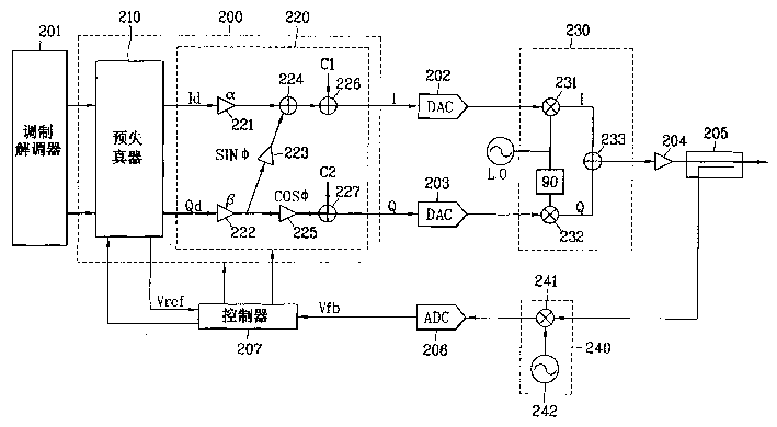
如图5所示,本发明的AQM误差补偿装置包括:预失真器210,用于使数字输入信号失真,以具有和非线性失真特性相反的特性;误差补偿单元220,用于预先根据误差校正信号来补偿从预失真器210输出的I/Q数字信号(Id,Qd);第一和第二数/模转换器202和203,用于把误差补偿单元220的I/Q数字信号转换为I/Q模拟信号;调制器230,用于把从第一和第二数/模转换器202和203输出的模拟信号调制为载波频率;功率放大器204,用于放大调制器230的输出信号,并将其提供给定向耦合器205;下变频器240,用于对从定向耦合器205输入的反馈信号进行下变频;模/数转换器206,用于把下变频器240的输出信号转换为数字信号;以及控制器207,用于对模/数转换器206的输出信号(Vfb)和从预失真器210输入的I/Q数字信号(Vref)进行比较,提取误差校正值,并向误差补偿单元220施加相应的误差校正信号。As shown in Figure 5, the AQM error compensation device of the present invention includes: a predistorter 210, used to distort the digital input signal to have a characteristic opposite to the nonlinear distortion characteristic; an error compensation unit 220, used to pre-correct according to the error signal to compensate the I/Q digital signal (Id, Qd) output from the predistorter 210; the first and second digital/analog converters 202 and 203 are used to convert the I/Q digital signal of the error compensation unit 220 into I/Q analog signal; Modulator 230, is used to modulate the analog signal output from first and second D/A converter 202 and 203 to carrier frequency; Power amplifier 204, is used to amplify the output signal of modulator 230, and provide it to the directional coupler 205; the down-converter 240 is used to down-convert the feedback signal input from the directional coupler 205; the analog/digital converter 206 is used to convert the output signal of the down-converter 240 into digital signal; and a controller 207 for comparing the output signal (Vfb) of the analog/digital converter 206 with the I/Q digital signal (Vref) input from the predistorter 210, extracting an error correction value, and reporting to the error The compensation unit 220 applies a corresponding error correction signal.
控制器207控制预失真器210,向系统施加用于提取AQM误差的测试信号,并通过所提取的AQM误差来计算AQM误差补偿值,向误差补偿单元220输出误差校正信号。The
控制器207控制预失真器210的信号和从预失真器207输入的用以计算AQM误差的参考信号(Vref)在控制器207和预失真器210之间交换。A signal for the
从而,控制器207对从定向耦合器205输入的反馈信号和从预失真器210输入的参考信号(Vref)进行比较,以提取误差,并输出用于补偿各个误差的误差补偿信号。Thus, the
误差补偿单元220包括:第一放大器221,用于控制已经根据第一增益校正信号(α)预失真的I数字信号(Id)的增益;第二放大器222,用于控制已经根据第二增益校正信号(β)预失真的Q数字信号(Qd)的增益;第三放大器223,用于根据第一相位校正信号(sinφ)来控制第二放大器222的输出信号的相位;第四放大器225,用于根据第二相位校正信号(cosφ)来控制第二放大器222的输出信号的相位;第一加法器224,用于对第一放大器221和第三放大器223的输出信号进行相加;第二加法器226,用于对第一加法器224的输出信号和第一DC偏移信号(C1)进行相加;以及第三加法器227,用于对第四放大器225的输出信号和第二DC偏移信号(C2)进行相加。The
调制器230包括:第一乘法器231,用于对从第一数/模转换器202输出的I模拟信号和从本机振荡器(LO)输出的本机震荡频率信号进行相乘;第二乘法器232,用于从第二数/模转换器203输出的Q模拟信号和从本机荡器(LO)输出的本机震荡频率信号进行相乘;以及合成器233,用于对第一和第二乘法器231和232的输出信号进行合成,并输出射频信号。The
以下说明如上所述构成的AQM误差补偿装置的操作。The operation of the AQM error compensating apparatus constructed as described above will be described below.
首先,预失真器210控制通过调制解调器201输入的数字信号,对I/Q数字信号(Id,Qd)进行预失真,以具有与功率放大器204的非线性失真特性相反的特性,并将它们输出到误差补偿单元220。First, the
误差补偿单元220校正从预失真器210输出的I/Q数字信号(Id,Qd)的误差,把它们施加到第一和第二数/模转换器202和203,第一和第二数/模转换器202和203把输入的I/Q数字信号转换为I/Q模拟信号,并输出它们。The
调制器230接收从第一和第二数/模转换器202和203输出的I/Q模拟信号,并对它们进行AQM调制。The
也就是说,调制器230的第一乘法器231对从第一数/模转换器202输出的I模拟信号和从本机振荡器(LO)输出的本机震荡频率信号进行相乘,第二乘法器232对从第二数/模转换器203输出的Q模拟信号和一个与本机震荡频率之间存在90度相位差的信号进行相乘。That is, the
每个上变频信号都被合成器233合成为射频信号,并被施加到功率放大器204。Each up-converted signal is combined into a radio frequency signal by the
下变频器240对经过功率放大器204从定向耦合器205输入的、反馈信号的频率进行下变频,并将其施加到模/数转换器206,模/数转换器206将下变频器240的输出信号转换为数字信号(Vfb),并将该数字信号输出到控制器207。The down-
控制器207对从预失真器210输入的I/Q数字信号(Vref)和从模/数转换器206接收到的I/Q数字信号进行一定的操作,以提取误差值,并向误差补偿单元220施加用于校正该误差值的误差校正信号。The
然后,误差补偿单元220根据误差校正信号来补偿I/Q数字信号的误差。Then, the
这时,误差校正信号包括:第一和第二DC偏移信号C1和C2,用于校正I/Q数字信号的DC偏移;第一和第二增益校正信号(α和β),用于校正I/Q数字信号的增益误差;以及相位校正信号(),用于校正I/Q数字信号的相位误差。At this time, the error correction signal includes: first and second DC offset signals C1 and C2, used to correct the DC offset of the I/Q digital signal; first and second gain correction signals (α and β), used for correcting the gain error of the I/Q digital signal; and a phase correction signal () for correcting the phase error of the I/Q digital signal.
图6是根据本发明的AQM误差补偿方法的流程图。FIG. 6 is a flow chart of the AQM error compensation method according to the present invention.
本发明的AQM误差补偿方法大致包括:从反馈I/Q数字信号中检测各DC偏移,消除反馈I/Q数字信号的DC偏移(步骤S41,S42);比较通过预失真器输入的参考信号,以检测增益校正值,对没有DC偏移的I/Q数字信号的增益进行补偿(步骤S43,S44,S45);利用通过预失真器输入的参考信号检测到延时值之后,补偿I/Q数字信号的延时(步骤S46,S47,S48,S49);利用经过了延时补偿的Q数字信号和通过预失真器输入的参考信号检测到相位校正值之后,将经过了延时补偿的Q数字信号平移该相位校正值(步骤S50,S51,S52)。The AQM error compensation method of the present invention generally includes: detecting each DC offset from the feedback I/Q digital signal, eliminating the DC offset of the feedback I/Q digital signal (steps S41, S42); signal, to detect the gain correction value, the gain of the I/Q digital signal without DC offset is compensated (step S43, S44, S45); after utilizing the reference signal input by the predistorter to detect the delay value, compensate I The time delay of/Q digital signal (step S46, S47, S48, S49); Utilize the Q digital signal that has passed through time delay compensation and after the reference signal that is input by predistorter detects phase correction value, will have passed through time delay compensation The Q digital signal shifts the phase correction value (steps S50, S51, S52).
以下参照图6,7,8,9和10对本发明的AQM误差补偿方法进行详细说明。The AQM error compensation method of the present invention will be described in detail below with reference to FIGS. 6 , 7 , 8 , 9 and 10 .
参照图7所示的消除DC偏移的处理,控制器207为通过模/数转换器206输入的一定数目的I/Q数字信号(Vfb:Vfb_I+jVfb_Q)提取各个平均值(步骤S61),从反馈I/Q数字信号(Vfb)中减去各平均值(步骤S62)。With reference to the processing of eliminating the DC offset shown in FIG. 7, the
控制器207根据该减法来检测差值作为第一和第二DC偏移(C1和C2)(步骤S63),并将其施加到误差补偿单元,从而消除反馈I/Q数字信号(Vfb)的DC偏移(步骤S64)。The
参照图8所示的补偿反馈I/Q数字信号(Vfb)的增益的处理。控制器207提取从预失真器201输入的参考I/Q数字信号(Vref)和反馈I/Q数字信号(Vfb)的绝对值(步骤S71),并计算参考I/Q数字信号的绝对值(|Vref|)和反馈I/Q数字信号的绝对值(|Vfb|)的各平均值(步骤S72)。Refer to the process of compensating the gain of the feedback I/Q digital signal (Vfb) shown in FIG. 8 . The
将参考I/Q数字信号(Vref)的平均值对反馈I/Q数字信号(Vfb)的平均值的比值乘以反馈I/Q数字信号(Vref),从而补偿增益(步骤S73和S74)。The gain is compensated by multiplying the ratio of the average value of the reference I/Q digital signal (Vref) to the average value of the feedback I/Q digital signal (Vfb) by the feedback I/Q digital signal (Vref) (steps S73 and S74).
检测经过了增益补偿的I数字信号的绝对值的平均值与反馈I数字信号绝对值的平均值的比值,作为第一增益校正信号(α),检测经过了增益补偿的Q数字信号的绝对值的平均值与反馈Q数字信号绝对值的平均值的比值,作为第二增益校正信号(β)(步骤S75),然后将第一各第二增益校正信号(α和β)分别乘以反馈I/Q数字信号,从而补偿增益失衡(步骤S76)。Detect the ratio of the average value of the absolute value of the I digital signal that has undergone gain compensation to the average value of the absolute value of the feedback I digital signal as the first gain correction signal (α), and detect the absolute value of the gain-compensated Q digital signal The ratio of the mean value of the mean value and the mean value of the absolute value of the feedback Q digital signal is used as the second gain correction signal (β) (step S75), and then the first and second gain correction signals (α and β) are respectively multiplied by the feedback I /Q digital signal, thereby compensating for gain imbalance (step S76).
为了补偿I/Q数字信号的相位失衡,应该补偿参考I数字信号(Vref_I)和反馈I数字信号(Vfb_I)之间的延时。In order to compensate the phase imbalance of the I/Q digital signal, the delay between the reference I digital signal (Vref_I) and the feedback I digital signal (Vfb_I) should be compensated.
使用以下原则补偿延时:假设参考I数字信号(Vref_I)和反馈I数字信号(Vfb_I)是相同的信号,并且存在延时,如果两个信号之间的差是‘0’,则它们是不存在延时的相同信号。Use the following principle to compensate for the delay: Assuming that the reference I digital signal (Vref_I) and the feedback I digital signal (Vfb_I) are the same signal and there is a delay, if the difference between the two signals is '0', they are not The same signal with a time delay.
但是,实际上,因为反馈I数字信号(Vfb_I)包含误差成分,当参考I数字信号(Vref_I)和反馈I数字信号(Vfb_I)之间的差最小时,确定延时已被补偿。Actually, however, since the feedback I digital signal (Vfb_I) contains error components, it is determined that the delay has been compensated when the difference between the reference I digital signal (Vref_I) and the feedback I digital signal (Vfb_I) is the smallest.
参照图9,以任意的过采样率(OSR)对参考I数字信号(Vref_I)和反馈I数字信号(Vfb_I)进行插值(步骤S81),对每个插值的参考I数字信号和反馈I数字信号进行相减,并累加减法值(步骤S82)。With reference to Fig. 9, carry out interpolation (step S81) to reference I digital signal (Vref_I) and feedback I digital signal (Vfb_I) with arbitrary oversampling rate (OSR), to the reference I digital signal of each interpolation and feedback I digital signal Subtraction is performed, and the subtraction value is accumulated (step S82).
这时,在两个信号的大小相同且没有时间差的理想状态下,减法值变成‘0’,而如果存在延时,则减法值具有对应于延时的值。At this time, in an ideal state where the magnitudes of the two signals are the same and there is no time difference, the subtraction value becomes '0', and if there is a delay, the subtraction value has a value corresponding to the delay.
在逐一增加‘k’(过采样率常数)的同时得到参考I数字信号和反馈I数字信号间差值累加和的运算可以由以下公式(2)表示:
图11A至11C是波形图,显示了根据值‘k’(过采样率常数)的增加,参考I数字信号和反馈I数字信号之间的变化。11A to 11C are waveform diagrams showing changes between the reference I digital signal and the feedback I digital signal according to an increase in the value 'k' (oversampling rate constant).
这时注意到,随着‘k’值的增加,两个信号间差值的累加和逐渐减小。Notice at this point that as the value of 'k' increases, the cumulative sum of the differences between the two signals gradually decreases.
也就是说,当通过改变‘k’值使差值累加和,即输出值,降到最小时(步骤S83),两个信号间的延时也最小。That is, when the cumulative sum of differences, ie, the output value, is minimized by changing the value of 'k' (step S83), the delay between the two signals is also minimized.
因此,通过将反馈I/Q数字信号平移如上所述计算的‘k’值,两个信号可以理想地对照(步骤S84)。Thus, by shifting the feedback I/Q digital signal by the 'k' value calculated as described above, the two signals can ideally be contrasted (step S84).
延时值可以由公式(3)表示: The delay value can be expressed by formula (3):
此后,通过利用经过了延时补偿的Q数字信号(Vfb_Q)和参考Q数字信号(Vref_Q),得到相位校正常数(j),将反馈Q数字信号(Vfb_Q)平移该相位校正常数(j)。Thereafter, by using the delay-compensated Q digital signal (Vfb_Q) and the reference Q digital signal (Vref_Q), the phase correction constant (j) is obtained, and the feedback Q digital signal (Vfb_Q) is shifted by the phase correction constant (j ).
也就是说,如图10所示,从参考Q数字信号(Vref_Q)中减去反馈Q数字信号(Vfb_Q)(步骤S91),得到减法值的累加和(步骤S92),然后,提取累加和的最小值作为相位校正常数(步骤S93)。将反馈Q数字信号(Vfb_Q)平移该相位校正常数(j),从而补偿两个信号之间的相位(步骤S94)。That is, as shown in FIG. 10, the feedback Q digital signal (Vfb_Q) is subtracted from the reference Q digital signal (Vref_Q) (step S91) to obtain the cumulative sum of the subtraction value (step S92), and then the sum of the cumulative sum is extracted. The minimum value is used as a phase correction constant (step S93). The feedback Q digital signal (Vfb_Q) is shifted by the phase correction constant (j), thereby compensating the phase between the two signals (step S94).
图12A和12B显示了AQM误差补偿之前和之后的参考I/Q数字信号(Vref_Q)。12A and 12B show the reference I/Q digital signal (Vref_Q) before and after AQM error compensation.
如图12A所示,与具有理想圆形的参考I/Q数字信号(S)相比,反馈I/Q数字信号(F1)具有倾斜的圆形,而如图12B所示,显示出经过了AQM误差补偿的I/Q数字信号(F2)被校正为几乎与参考I/Q数字信号(S)一致的圆形。As shown in FIG. 12A, the feedback I/Q digital signal (F1) has a sloped circular shape compared to the reference I/Q digital signal (S) which has an ideal circular shape, while as shown in FIG. 12B, it is shown that after The AQM error-compensated I/Q digital signal (F2) is corrected to a circular shape that almost coincides with the reference I/Q digital signal (S).
如上所述,本发明的AQM误差补偿装置和方法具有很多优点。As described above, the AQM error compensation apparatus and method of the present invention have many advantages.
例如,第一,可以通过在一定的系统初始时间中利用正弦波提取DC偏移及增益,以及相位误差校正值,来补偿AQM误差,即使信号在变化了之后再传输,也可以通过比较输入的参考信号和反馈信号,并提取各个误差的校正值,来补偿AQM误差。因此,可以根据误差的发生状况来精确地进行补偿。For example, firstly, AQM error can be compensated by extracting DC offset and gain and phase error correction value by using sine wave in a certain system initial time. Reference signal and feedback signal, and extract the correction value of each error to compensate for AQM error. Therefore, it is possible to accurately perform compensation according to occurrence conditions of errors.
第二,用数字方法来提取用于测量AQM误差的反馈数字信号,以消除由非线性特性引起的AQM误差计算误差,从而可以减小AQM误差补偿中所产生的因为工作区域和非线性特性引起的误差。Second, the digital method is used to extract the feedback digital signal used to measure the AQM error to eliminate the AQM error calculation error caused by the nonlinear characteristics, so that the AQM error compensation caused by the working area and nonlinear characteristics can be reduced. error.
最后,无需使用延时装置就可以补偿延时,从而可以降低产品的单位成本,并可以提高信号的可再生性。Finally, the time delay can be compensated without using a delay device, so that the unit cost of the product can be reduced and the reproducibility of the signal can be improved.
前面所述的实施例和优点仅仅是示例性的,并不构成对本发明的限制。本发明的教导可以容易地应用于其它类型的设备。本发明的说明书是说明性的,并不限制权利要求的范围。对于本领域的技术人员,显然可以有很多替换、改进和变化。在权利要求书中,装置加功能的语句旨在涵盖实现所述功能的结构,其不仅是结构等同的,也包括等同的结构。The foregoing embodiments and advantages are merely exemplary and do not constitute a limitation of the present invention. The teachings of the present invention can be readily applied to other types of devices. The description of the present invention is illustrative and does not limit the scope of the claims. Many alternatives, improvements and changes will be apparent to those skilled in the art. In the claims, means-plus-function clauses are intended to cover structures as performing the recited function and not only structural equivalents but also equivalent structures.
Claims (20)
Applications Claiming Priority (4)
| Application Number | Priority Date | Filing Date | Title |
|---|---|---|---|
| KR30855/2001 | 2001-06-01 | ||
| KR10-2001-0030855A KR100386287B1 (en) | 2001-06-01 | 2001-06-01 | Compensating metod for time delay of digital linearization apparatus |
| KR10-2001-0084320A KR100414075B1 (en) | 2001-12-24 | 2001-12-24 | Error compensation apparatus and method for aqm |
| KR84320/2001 | 2001-12-24 |
Publications (1)
| Publication Number | Publication Date |
|---|---|
| CN1389987A true CN1389987A (en) | 2003-01-08 |
Family
ID=26639118
Family Applications (1)
| Application Number | Title | Priority Date | Filing Date |
|---|---|---|---|
| CN02122146.4A Pending CN1389987A (en) | 2001-06-01 | 2002-05-31 | Analogue quadrature moducator error compensating apparatus and method |
Country Status (2)
| Country | Link |
|---|---|
| US (1) | US20020181611A1 (en) |
| CN (1) | CN1389987A (en) |
Cited By (16)
| Publication number | Priority date | Publication date | Assignee | Title |
|---|---|---|---|---|
| CN100356280C (en) * | 2004-12-30 | 2007-12-19 | 杭州和利时自动化有限公司 | Dynamic compensation method for distortion measurement in discrete control and control system thereof |
| CN100384269C (en) * | 2004-02-25 | 2008-04-23 | 华为技术有限公司 | A system and method for compensating non-ideal characteristics of a base station transmitter |
| CN101061633B (en) * | 2004-03-25 | 2010-05-05 | 奥普蒂科伦公司 | Model-Based Distortion Reduction Method and System for Power Amplifiers |
| CN101272373B (en) * | 2008-05-07 | 2010-09-08 | 北京北方烽火科技有限公司 | An adaptive analog quadrature modulation imbalance compensation method and device |
| CN101119357B (en) * | 2006-09-07 | 2011-01-12 | 威盛电子股份有限公司 | Transmitter and transmitter error compensation method |
| CN101411055B (en) * | 2006-03-27 | 2011-11-09 | Nxp股份有限公司 | Radio frequency PWM & PPM modulator |
| CN101895259B (en) * | 2009-05-18 | 2013-01-02 | 富士通株式会社 | Predistorter, predistortion method and predistortion system |
| CN102969985A (en) * | 2011-08-31 | 2013-03-13 | 苹果公司 | Calibration systems for wireless electronic devices |
| CN101345783B (en) * | 2008-08-22 | 2013-03-27 | 北京中星微电子有限公司 | System and method for noise elimination |
| CN104065370A (en) * | 2013-03-15 | 2014-09-24 | 安捷伦科技有限公司 | Adjustable directional coupler circuit |
| CN104124928A (en) * | 2013-04-26 | 2014-10-29 | 瑞昱半导体股份有限公司 | Automatic gain adjustment device and method thereof |
| CN105007091A (en) * | 2011-04-14 | 2015-10-28 | 联发科技股份有限公司 | Transmitter and Compensation Method |
| CN107251420A (en) * | 2015-02-27 | 2017-10-13 | 阿尔卡特朗讯 | The vector signal handled using the digital vector of vector is aligned |
| CN109998521A (en) * | 2017-11-30 | 2019-07-12 | 韦伯斯特生物官能(以色列)有限公司 | The method and apparatus of fast quick-recovery ECG signal |
| CN110212997A (en) * | 2019-06-04 | 2019-09-06 | 成都德芯数字科技股份有限公司 | A kind of acquisition methods and device for modulating the bit error rate |
| CN114172497A (en) * | 2021-12-06 | 2022-03-11 | 中国人民解放军国防科技大学 | A 5-level radio frequency pulse width modulation method and modulator without spectral aliasing |
Families Citing this family (35)
| Publication number | Priority date | Publication date | Assignee | Title |
|---|---|---|---|---|
| US7248625B2 (en) * | 2002-09-05 | 2007-07-24 | Silicon Storage Technology, Inc. | Compensation of I-Q imbalance in digital transceivers |
| US7333557B2 (en) * | 2002-12-16 | 2008-02-19 | Nortel Networks Limited | Adaptive controller for linearization of transmitter with impairments |
| JP4175503B2 (en) * | 2003-04-18 | 2008-11-05 | ソニー・エリクソン・モバイルコミュニケーションズ株式会社 | Distortion compensation circuit and transmitter |
| US6781537B1 (en) * | 2003-06-10 | 2004-08-24 | Nortel Networks Limited | High speed digital to analog converter |
| GB2408860B (en) * | 2003-12-04 | 2006-12-20 | Motorola Inc | Wireless communication unit, linearised transmitter circuit and method of linearising therein |
| US20050163249A1 (en) * | 2004-01-27 | 2005-07-28 | Crestcom, Inc. | Predistortion circuit and method for compensating linear distortion in a digital RF communications transmitter |
| US7349677B2 (en) * | 2004-04-08 | 2008-03-25 | Broadcom Corporation | Hardware efficient RF transceiver I/Q imbalance compensation based upon taylor approximation |
| DE602004029941D1 (en) * | 2004-05-19 | 2010-12-16 | Ericsson Telefon Ab L M | ADAPTIVE FORECASTING METHOD AND ARRANGEMENT |
| US7197087B2 (en) * | 2004-07-09 | 2007-03-27 | Powerwave Technologies, Inc. | System and method for differential IQ delay compensation in a communications system utilizing adaptive AQM compensation |
| CA2576778C (en) * | 2006-02-07 | 2014-09-02 | Xinping Huang | Self-calibrating multi-port circuit and method |
| US7796960B1 (en) | 2006-04-04 | 2010-09-14 | Nortel Networks Limited | Signal transmitter linearization |
| US8995502B1 (en) | 2006-04-04 | 2015-03-31 | Apple Inc. | Transceiver with spectral analysis |
| US8498590B1 (en) | 2006-04-04 | 2013-07-30 | Apple Inc. | Signal transmitter linearization |
| US8886341B1 (en) | 2006-04-04 | 2014-11-11 | Microsoft Corporation | Adaptive sample-by-sample controller for under-determined systems |
| US20080063041A1 (en) * | 2006-09-08 | 2008-03-13 | Noam Galperin | Fast training equalization of a signal |
| JP2010504678A (en) * | 2006-09-20 | 2010-02-12 | エヌエックスピー ビー ヴィ | Method and system for calibrating an analog I/Q modulator in a transmitter - Patents.com |
| GB2442773A (en) * | 2006-10-11 | 2008-04-16 | Tandberg Television Asa | Canceling distortion |
| US8139676B2 (en) * | 2007-01-17 | 2012-03-20 | Motorola Solutions, Inc. | Wireless communication unit, linearised transmitter circuit and method of linearising therein |
| US8175553B2 (en) * | 2007-01-17 | 2012-05-08 | Motorola Solutions, Inc. | Wireless communication unit, linearised transmitter circuit and method of linearising therein |
| US7941106B2 (en) * | 2007-05-10 | 2011-05-10 | Skyworks Solutions, Inc. | Systems and methods for controlling local oscillator feed-through |
| US8073046B2 (en) * | 2007-06-14 | 2011-12-06 | Zoran Corporation | Fast training equalization of a signal by using adaptive-iterative algorithm with main path phase correction |
| US8160191B2 (en) * | 2008-12-01 | 2012-04-17 | Rockstar Bidco Lp | Correction of quadrature errors |
| US8462881B2 (en) * | 2008-12-31 | 2013-06-11 | Ubidyne, Inc. | Method for digitally predistorting a payload signal and radio station incorporating the method |
| JP5158034B2 (en) * | 2009-08-12 | 2013-03-06 | 富士通株式会社 | Wireless device and signal processing method |
| CN102130697B (en) * | 2010-01-20 | 2015-05-27 | 华为技术有限公司 | Receiver, transmitter and feedback device, transceiver and signal processing method |
| US20110235749A1 (en) * | 2010-03-26 | 2011-09-29 | Peter Kenington | Active antenna array having analogue transmitter linearisation and a method for predistortion of radio signals |
| US20110235748A1 (en) * | 2010-03-26 | 2011-09-29 | Peter Kenington | Active antenna array having analogue transmitter linearisation and a method for predistortion of radio signals |
| US20110235734A1 (en) * | 2010-03-26 | 2011-09-29 | Peter Kenington | Active antenna array having a single dpd lineariser and a method for predistortion of radio signals |
| US9002310B2 (en) * | 2010-09-28 | 2015-04-07 | Intel Mobile Communications GmbH | IP2 calibration methods and techniques |
| TWI466506B (en) * | 2012-02-22 | 2014-12-21 | Realtek Semiconductor Corp | Method for compensating mismatch of in-phase signal and quadrature signal of transmitter/receiver |
| EP3031141B8 (en) * | 2013-08-09 | 2018-05-16 | Kumu Networks, Inc. | Cancellation of non-linear digital self-interferences |
| CN107078702B (en) * | 2014-11-19 | 2019-11-29 | 华为技术有限公司 | A kind of device and method of pre-distortion |
| US9413583B2 (en) * | 2014-12-18 | 2016-08-09 | Intel IP Corporation | Calibrating RF path delay and IQ phase imbalance for polar transmit system |
| US9509350B1 (en) * | 2015-06-11 | 2016-11-29 | Infineon Technologies Ag | Devices and methods for adaptive crest factor reduction in dynamic predistortion |
| AU2024219408A1 (en) * | 2024-07-15 | 2026-02-05 | Morse Micro Pty. Ltd. | Compensation methods and devices for digital power amplifier |
Family Cites Families (6)
| Publication number | Priority date | Publication date | Assignee | Title |
|---|---|---|---|---|
| US5574751A (en) * | 1995-04-24 | 1996-11-12 | Motorola, Inc. | Method for a soft-decision modulation system |
| US5913172A (en) * | 1996-11-15 | 1999-06-15 | Glenayre Electronics, Inc. | Method and apparatus for reducing phase cancellation in a simulcast paging system |
| US5923712A (en) * | 1997-05-05 | 1999-07-13 | Glenayre Electronics, Inc. | Method and apparatus for linear transmission by direct inverse modeling |
| US6177893B1 (en) * | 1998-09-15 | 2001-01-23 | Scott R. Velazquez | Parallel processing analog and digital converter |
| GB2346776B (en) * | 1999-02-13 | 2001-09-12 | Motorola Ltd | Synchronisation lock detector and method |
| US6751447B1 (en) * | 1999-12-30 | 2004-06-15 | Samsung Electronics Cop., Ltd. | Adaptive digital pre-distortion circuit using output reference signal and method of operation |
-
2002
- 2002-05-31 CN CN02122146.4A patent/CN1389987A/en active Pending
- 2002-05-31 US US10/157,929 patent/US20020181611A1/en not_active Abandoned
Cited By (24)
| Publication number | Priority date | Publication date | Assignee | Title |
|---|---|---|---|---|
| CN100384269C (en) * | 2004-02-25 | 2008-04-23 | 华为技术有限公司 | A system and method for compensating non-ideal characteristics of a base station transmitter |
| CN101061633B (en) * | 2004-03-25 | 2010-05-05 | 奥普蒂科伦公司 | Model-Based Distortion Reduction Method and System for Power Amplifiers |
| CN100356280C (en) * | 2004-12-30 | 2007-12-19 | 杭州和利时自动化有限公司 | Dynamic compensation method for distortion measurement in discrete control and control system thereof |
| CN101411055B (en) * | 2006-03-27 | 2011-11-09 | Nxp股份有限公司 | Radio frequency PWM & PPM modulator |
| CN101119357B (en) * | 2006-09-07 | 2011-01-12 | 威盛电子股份有限公司 | Transmitter and transmitter error compensation method |
| US7881402B2 (en) | 2006-09-07 | 2011-02-01 | Via Technologies, Inc. | Compensation for gain imbalance, phase imbalance and DC offsets in a transmitter |
| CN101272373B (en) * | 2008-05-07 | 2010-09-08 | 北京北方烽火科技有限公司 | An adaptive analog quadrature modulation imbalance compensation method and device |
| CN101345783B (en) * | 2008-08-22 | 2013-03-27 | 北京中星微电子有限公司 | System and method for noise elimination |
| CN101895259B (en) * | 2009-05-18 | 2013-01-02 | 富士通株式会社 | Predistorter, predistortion method and predistortion system |
| CN105007091B (en) * | 2011-04-14 | 2018-06-19 | 联发科技股份有限公司 | Transceiver and compensation method |
| CN105007091A (en) * | 2011-04-14 | 2015-10-28 | 联发科技股份有限公司 | Transmitter and Compensation Method |
| CN102969985B (en) * | 2011-08-31 | 2015-10-21 | 苹果公司 | The calibration system of radio-based electronic devices |
| CN102969985A (en) * | 2011-08-31 | 2013-03-13 | 苹果公司 | Calibration systems for wireless electronic devices |
| CN104065370A (en) * | 2013-03-15 | 2014-09-24 | 安捷伦科技有限公司 | Adjustable directional coupler circuit |
| CN104065370B (en) * | 2013-03-15 | 2018-11-09 | 是德科技股份有限公司 | Transvar coupler circuit |
| CN104124928A (en) * | 2013-04-26 | 2014-10-29 | 瑞昱半导体股份有限公司 | Automatic gain adjustment device and method thereof |
| CN104124928B (en) * | 2013-04-26 | 2017-08-01 | 瑞昱半导体股份有限公司 | Automatic gain adjustment device and method thereof |
| CN107251420A (en) * | 2015-02-27 | 2017-10-13 | 阿尔卡特朗讯 | The vector signal handled using the digital vector of vector is aligned |
| CN107251420B (en) * | 2015-02-27 | 2021-01-22 | 阿尔卡特朗讯 | Method, apparatus and non-transitory computer readable medium for vector signal alignment |
| CN109998521A (en) * | 2017-11-30 | 2019-07-12 | 韦伯斯特生物官能(以色列)有限公司 | The method and apparatus of fast quick-recovery ECG signal |
| CN109998521B (en) * | 2017-11-30 | 2024-04-16 | 韦伯斯特生物官能(以色列)有限公司 | Method and device for quickly restoring ECG signals |
| CN110212997A (en) * | 2019-06-04 | 2019-09-06 | 成都德芯数字科技股份有限公司 | A kind of acquisition methods and device for modulating the bit error rate |
| CN114172497A (en) * | 2021-12-06 | 2022-03-11 | 中国人民解放军国防科技大学 | A 5-level radio frequency pulse width modulation method and modulator without spectral aliasing |
| CN114172497B (en) * | 2021-12-06 | 2023-08-15 | 中国人民解放军国防科技大学 | Spectrum aliasing-free 5-level radio frequency pulse width modulation method and modulator |
Also Published As
| Publication number | Publication date |
|---|---|
| US20020181611A1 (en) | 2002-12-05 |
Similar Documents
| Publication | Publication Date | Title |
|---|---|---|
| CN1389987A (en) | Analogue quadrature moducator error compensating apparatus and method | |
| CN1285169C (en) | Predistortion digital linearization circuit and its gain control method | |
| CN1252910C (en) | Communications systems | |
| US7039124B2 (en) | Apparatus and method for compensating for analog quadrature modulation error | |
| US6973138B1 (en) | Advanced adaptive pre-distortion in a radio frequency transmitter | |
| CN1169309C (en) | Adaptive Predistortion Transmitter | |
| US7869543B2 (en) | System and method for synchronization, power control, calibration, and modulation in communication transmitters | |
| CN1969459A (en) | Digital predistortion system and method for linearizing an RF power amplifier with nonlinear gain characteristics and memory effects | |
| KR100429981B1 (en) | Aqm error compensation apparatus and method | |
| CN1663214A (en) | Amplitude imbalance compensation of quadrature modulator | |
| US8280327B2 (en) | Receiver capable of reducing local oscillation leakage and in-phase/quadrature-phase (I/Q) mismatch and an adjusting method thereof | |
| CN1387697A (en) | Lineariser for signal handling apparatus | |
| CN1604577A (en) | Transmitting device with adaptive digital predistortion, transceiver with the same and method of operating the same | |
| US10382073B2 (en) | Analog RF pre-distorter and non-linear splitter | |
| US7646238B2 (en) | Amplification apparatus | |
| US20020012404A1 (en) | Predistortion linearizer and method thereof | |
| CN101080911A (en) | Calibrating amplitude and phase imbalance and DC offset of an analog i /q modulator in a high-frequency transmitter | |
| CN1638292A (en) | Transmitting device | |
| US7613251B2 (en) | Distortion compensating apparatus and method | |
| CN1666408A (en) | Predistortion control | |
| CN1340911A (en) | Method and device for distortion compensation | |
| US20090174456A1 (en) | DC Offset Correcting Device And DC Offset Correcting Method | |
| CN103532499B (en) | Device for compensation of distortion and distortion compensating method | |
| KR100414075B1 (en) | Error compensation apparatus and method for aqm | |
| JP4533759B2 (en) | Data converter, data conversion method, and transmission circuit, communication device, and electronic device using the same |
Legal Events
| Date | Code | Title | Description |
|---|---|---|---|
| C10 | Entry into substantive examination | ||
| SE01 | Entry into force of request for substantive examination | ||
| C06 | Publication | ||
| PB01 | Publication | ||
| C10 | Entry into substantive examination | ||
| SE01 | Entry into force of request for substantive examination | ||
| ASS | Succession or assignment of patent right |
Owner name: LG- NORTEL CO., LTD. Free format text: FORMER OWNER: LG ELECTRONIC CO., LTD. Effective date: 20061020 |
|
| C41 | Transfer of patent application or patent right or utility model | ||
| TA01 | Transfer of patent application right |
Effective date of registration: 20061020 Address after: Seoul, South Kerean Applicant after: LG Nortel Co., Ltd. Address before: Seoul, South Kerean Applicant before: LG Electronics Inc. |
|
| C02 | Deemed withdrawal of patent application after publication (patent law 2001) | ||
| WD01 | Invention patent application deemed withdrawn after publication |