CN1340859A - Chip type semiconductor device - Google Patents
Chip type semiconductor device Download PDFInfo
- Publication number
- CN1340859A CN1340859A CN01124289A CN01124289A CN1340859A CN 1340859 A CN1340859 A CN 1340859A CN 01124289 A CN01124289 A CN 01124289A CN 01124289 A CN01124289 A CN 01124289A CN 1340859 A CN1340859 A CN 1340859A
- Authority
- CN
- China
- Prior art keywords
- semiconductor
- electrodes
- insulating resin
- semiconductor chip
- semiconductor device
- Prior art date
- Legal status (The legal status is an assumption and is not a legal conclusion. Google has not performed a legal analysis and makes no representation as to the accuracy of the status listed.)
- Pending
Links
Images


Classifications
-
- H10W70/20—
-
- H10W74/01—
-
- H—ELECTRICITY
- H10—SEMICONDUCTOR DEVICES; ELECTRIC SOLID-STATE DEVICES NOT OTHERWISE PROVIDED FOR
- H10D—INORGANIC ELECTRIC SEMICONDUCTOR DEVICES
- H10D62/00—Semiconductor bodies, or regions thereof, of devices having potential barriers
- H10D62/10—Shapes, relative sizes or dispositions of the regions of the semiconductor bodies; Shapes of the semiconductor bodies
- H10D62/117—Shapes of semiconductor bodies
-
- H10W74/129—
Landscapes
- Dicing (AREA)
- Encapsulation Of And Coatings For Semiconductor Or Solid State Devices (AREA)
- Structures Or Materials For Encapsulating Or Coating Semiconductor Devices Or Solid State Devices (AREA)
Abstract
一种具有多个正面突出电极和多个背面薄膜电极的半导体芯片。正面电极与金属膜制成的互连线连接。通过将背面薄膜电极安装在印刷电路板的各端子上而将该半导体芯片安装在印刷电路板上,将金属膜用焊丝与印刷电路板的其它端子连接。可以在简单的工艺中一次制造大量的半导体芯片。
A semiconductor chip having a plurality of front protruding electrodes and a plurality of back thin film electrodes. The front electrode is connected to an interconnection line made of a metal film. The semiconductor chip is mounted on the printed circuit board by mounting the back thin film electrode on each terminal of the printed circuit board, and the metal film is connected to other terminals of the printed circuit board with soldering wire. A large number of semiconductor chips can be manufactured at one time in a simple process.
Description
本发明涉及芯片型半导体器件及其制造方法。The present invention relates to a chip-type semiconductor device and a manufacturing method thereof.
相关技术的说明Description of related technologies
对于便携式电子设备如摄像机和笔记本电脑,人们总是希望它们的尺寸更小和重量更轻。因此,也要求在这些便携式电子设备中使用的半导体器件尽可能地小。为了得到这种更小的尺寸,一些半导体器件具有引线框结构,而为了得到更小的尺寸,其它的半导体器件具有诸如在JP-A-58-218142中披露的另外的结构。For portable electronic devices such as video cameras and notebook computers, it is always desired that they be smaller in size and lighter in weight. Therefore, semiconductor devices used in these portable electronic devices are also required to be as small as possible. To achieve such a smaller size, some semiconductor devices have a lead frame structure, and to achieve a smaller size, other semiconductor devices have another structure such as disclosed in JP-A-58-218142.
为了得到在上述公报中所描述的结构,具有开口阵列的树脂栅格框被粘合到金属板上,以形成各单元分隔区的底板,然后在各单元分隔区的底板上放置半导体芯片。然后单元分隔区的各顶部开口被扁平的盖所盖住以将各单元分隔区中的半导体芯片封装。然后通过将栅格框与金属板一起切割来分开单元分隔区,以得到分离的具有更小尺寸的半导体芯片组件。该过程是一次制造大量半导体器件的常规工艺;但是,其缺点是难以在单个步骤中切割树脂栅格框与金属底板。In order to obtain the structure described in the above publication, a resin grid frame having an array of openings is bonded to a metal plate to form a base plate of each cell compartment, and then a semiconductor chip is placed on the base plate of each cell compartment. The respective top openings of the cell separation regions are then covered with flat caps to package the semiconductor chips in the respective cell separation regions. The cell separation regions are then separated by cutting the grid frame together with the metal plate to obtain separated semiconductor chip assemblies having smaller sizes. This process is a conventional process for manufacturing a large number of semiconductor devices at one time; however, its disadvantage is that it is difficult to cut the resin grid frame and the metal base plate in a single step.
专利公报JP3033576公开了另一种用于一次制造大量半导体器件的工艺。图1显示了通过该工艺得到的半导体器件,其中半导体芯片11包括MOSFET(未示出),其具有在芯片背面的源和栅电极12a和12b,一覆盖半导体芯片11的除电极12a和12b顶部之外的背面和侧面的绝缘树脂膜13,以及由导电树脂制成并从芯片的前面伸向背面的漏电极14,以及一覆盖半导体器件正面和侧面的整体树脂涂层23。该半导体器件安装在印刷电路板上,并且半导体器件的背面向着印刷电路板。Patent publication JP3033576 discloses another process for manufacturing a large number of semiconductor devices at one time. Fig. 1 has shown the semiconductor device that obtains by this process, and wherein
该芯片型半导体器件是通过如下步骤得到的:将包括多个芯片的半导体晶片粘合到粘性薄片上;在一个方向上切割该晶片以形成多个带状的芯片组,每个芯片组包括多个沿一个方向排列的芯片;将粘性薄片延展以扩大芯片组之间的间距;将绝缘树脂加到晶片的整个顶部表面,而露出源和栅电极;将芯片组翻转并将芯片组粘附到带子上,然后去掉粘性薄片;切割芯片组之间的绝缘树脂;将导电树脂加到整个顶部表面上并对其构图;切割芯片组之间的导电树脂和绝缘树脂;切割芯片组以形成多个分开的芯片;以及形成半导体芯片的正面和侧面上的整个涂层。The chip-type semiconductor device is obtained by bonding a semiconductor wafer including a plurality of chips to an adhesive sheet; cutting the wafer in one direction to form a plurality of strip-shaped chip groups each including a plurality of chips aligned in one direction; stretch the adhesive sheet to expand the spacing between the chipsets; apply insulating resin to the entire top surface of the wafer, exposing the source and gate electrodes; flip the chipsets over and attach the chipsets to tape, then remove the adhesive sheet; cut the insulating resin between chipsets; apply and pattern conductive resin to the entire top surface; cut conductive and insulating resins between chipsets; cut chipsets to form multiple separate chips; and form the entire coating on the front and sides of the semiconductor chips.
上述获得的芯片型半导体器件的优点是尺寸更小并且可以用表面安装技术安装到印刷电路板上。但是,在该专利公报公开的芯片型半导体器件中,其工艺步骤数量的减少以及由此而带来的制造成本降低都是不足的。The chip-type semiconductor device obtained above has the advantage of being smaller in size and can be mounted on a printed circuit board using surface mount technology. However, in the chip-type semiconductor device disclosed in this patent publication, the reduction in the number of process steps and the resulting reduction in manufacturing cost are insufficient.
发明的概述Overview of the invention
考虑到现有技术的上述问题,本发明的一个目的是提供一种芯片型半导体器件,其具有更小的尺寸,并且能够在单个工艺中一次制造大量的半导体器件,从而以较低的成本来制造这种半导体器件。In view of the above-mentioned problems of the prior art, an object of the present invention is to provide a chip-type semiconductor device which has a smaller size and can manufacture a large number of semiconductor devices at a time in a single process, thereby manufacturing at a lower cost. Such a semiconductor device is manufactured.
本发明提供一种包括半导体芯片的半导体器件,在半导体芯片背面有多个薄膜电极,在半导体芯片正面有多个突出电极,一绝缘树脂膜覆盖半导体芯片而露出薄膜电极以及各突出电极的顶部,在突出电极上形成导电膜并由该导电膜形成多个互连线。The present invention provides a semiconductor device comprising a semiconductor chip. There are a plurality of thin film electrodes on the back of the semiconductor chip, and a plurality of protruding electrodes on the front of the semiconductor chip. An insulating resin film covers the semiconductor chip to expose the thin film electrodes and the tops of the protruding electrodes. A conductive film is formed on the protruding electrodes and a plurality of interconnect lines are formed from the conductive film.
本发明还提供一种制造半导体器件的方法,包括如下步骤:将半导体晶片粘合到粘性薄片上,该半导体晶片背面具有多个膜电极,而正面具有多个突出电极,背面与粘性薄片接触;切割半导体晶片以形成多个半导体芯片,每个半导体芯片包括多个膜电极和多个突出电极;延展粘性薄片以扩大每两个半导体芯片之间的间距;施加液体绝缘树脂以覆盖粘性薄片上的半导体芯片,并填充它们之间的间隙;固化液体绝缘树脂;去除部分的绝缘树脂以使突出电极的顶部表面从该树脂中露出;在突出电极的顶部表面上和在绝缘树脂上形成导电膜;将绝缘树脂和粘性薄片划片,以分离半导体芯片。The present invention also provides a method of manufacturing a semiconductor device, comprising the steps of: adhering a semiconductor wafer to an adhesive sheet, the semiconductor wafer has a plurality of membrane electrodes on the back and a plurality of protruding electrodes on the front, and the back is in contact with the adhesive sheet; Cutting a semiconductor wafer to form a plurality of semiconductor chips each including a plurality of film electrodes and a plurality of protruding electrodes; stretching the adhesive sheet to enlarge the space between every two semiconductor chips; applying liquid insulating resin to cover the semiconductor chips, and filling a gap therebetween; curing the liquid insulating resin; removing part of the insulating resin so that the top surfaces of the protruding electrodes are exposed from the resin; forming a conductive film on the top surfaces of the protruding electrodes and on the insulating resin; The insulating resin and adhesive sheet are diced to separate semiconductor chips.
根据本发明的半导体器件及由本发明方法制造的半导体器件,可以在简单的工艺中一次制造大量的半导体器件,从而减少制造这种半导体器件的成本。According to the semiconductor device of the present invention and the semiconductor device manufactured by the method of the present invention, a large number of semiconductor devices can be manufactured at one time in a simple process, thereby reducing the cost of manufacturing such semiconductor devices.
本发明的上述目的、特点及优点将通过下面参考附图进行的说明而变得更为清楚。The above objects, features and advantages of the present invention will become more apparent from the following description with reference to the accompanying drawings.
附图的简要说明Brief description of the drawings
图1是常规的芯片型半导体器件的剖视图;1 is a cross-sectional view of a conventional chip-type semiconductor device;
图2是根据本发明一实施例的芯片型半导体器件的剖视图;2 is a cross-sectional view of a chip-type semiconductor device according to an embodiment of the present invention;
图3至图7是图2所示芯片型半导体器件的剖视和侧视图,分别显示了制造工艺的制造步骤;3 to 7 are cross-sectional and side views of the chip-type semiconductor device shown in FIG. 2, respectively showing manufacturing steps of the manufacturing process;
图8是图2所示芯片型半导体器件的改型的剖视图;8 is a cross-sectional view of a modification of the chip-type semiconductor device shown in FIG. 2;
图9是图2所示芯片型半导体器件的另一改型的剖视图。FIG. 9 is a cross-sectional view of another modification of the chip-type semiconductor device shown in FIG. 2 .
本发明的优选实施例Preferred Embodiments of the Invention
现在,将参考附图更详细地说明本发明,其中相似的构成单元以相似的参考标号指示。Now, the present invention will be explained in more detail with reference to the accompanying drawings, in which like constituent elements are denoted by like reference numerals.
参考图2,根据本发明一实施例的芯片型半导体器件包括:半导体芯片15,在半导体芯片15的背面有多个薄膜电极15a,从半导体芯片15正面伸出有多个正面凸起电极15b;形成在半导体芯片15的整个表面上的绝缘树脂膜16,其露出薄膜电极15a以及各正面凸起电极15b的顶部表面;以及在半导体芯片15的正面侧、或是在正面凸起电极15b的顶部表面上形成的导电树脂膜17。导电树脂膜17构成为与正面凸起电极15b连接的多个互连线。Referring to FIG. 2, a chip-type semiconductor device according to an embodiment of the present invention includes: a
图2所示的半导体器件安装在印刷电路板上,其背面电极15a安装在印刷电路板各端子上以用于电连接。构成互连线的导电膜17还通过焊丝与印刷电路板的端子连接。在另一种方式中,半导体器件可以夹在一对印刷电路板之间,其背面电极15a安装在印刷电路板之一的端子上,而导电膜17与另一个印刷电路板的端子连接。The semiconductor device shown in FIG. 2 is mounted on a printed circuit board, and its
图2的半导体器件通过下面结合图3至图7详细说明的工艺来制造。The semiconductor device of FIG. 2 is manufactured through the processes described in detail below with reference to FIGS. 3 to 7 .
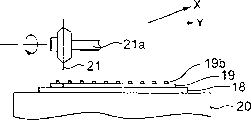
半导体晶片19在其正面具有多个凸起电极(突出电极)19b,在其背面具有多个薄膜电极19a。该半导体晶片19粘合在具有弹性或延展属性的粘性绝缘薄片18上,如图3所示。薄膜电极19a与粘性薄片18相对。The
在粘性薄片18上得到的晶片被放在工作台20上,工作台20在Y方向上以步进方式移动,在行进到终点后转动90度,然后在相反方向上以步进方式移动。在工作台20上方设置转动刀片21,用于围绕转动轴21a转动,并在平行于工作台20表面的X方向上往复地运动。转动刀片21被提供用于冷却刀片21的冷却水和用于去除转动刀片21对半导体晶片19划片所产生微粒的清洗水。The wafer obtained on the
半导体晶片19利用工作台20和相关的转动刀片21的运动而进行划片,而粘性薄片18被固定在工作台20上,从而形成在粘性薄片18上排列的分开的半导体芯片15的阵列,如图4所示。
然后将所得到的在粘性薄片18上的芯片阵列从工作台20中取出,并且将粘性薄片18在半导体芯片排列的对角线方向上延展。这使得每两个半导体芯片之间的间隙增大,如图5所示。在图5中,图4所示的凸起电极19b和薄膜电极19a分别由符号15b和15a指示。The resulting array of chips on the
接着,如图6所示,将液体或糊状树脂16施加到被划片的半导体晶片的整个表面上,以由此填充每两个半导体芯片之间的间隙,并覆盖半导体芯片15的包括凸起电极15b在内的整个顶部表面。所得到的液体树脂膜16的表面在每两个半导体芯片之间的间隙上具有微小的凹陷,形成一定程度的栅格结构,从而造成了凸起电极15b上的树脂膜16的部分厚度较小。树脂膜在此状态固化。Next, as shown in FIG. 6, a liquid or
然后用研磨机对所得到的结构进行研磨,研磨机将树脂膜16研磨到凸起电极15b的上表面露出为止。然后将所得到的结构转移蒸发反应器中,以在树脂膜16的整个表面上和凸起电极15b的顶部表面形成金属膜17。然后将金属膜17构图以形成多个互连线。另外,金属膜17的蒸发可以用掩模图形来进行,以将金属膜构成为互连线。金属膜17与凸起电极15b电连接,从而与背面电极15a一起形成为半导体芯片15的外部电极。用于金属膜(或导电膜)的材料优选根据用于键合的材料而从金、铜和铝中选择。如果使用焊料进行键合,则优选使用金或铜作为导电膜17的材料。The resulting structure is then ground with a grinder that grinds the
然后在X和Y方向上将所得到的结构划片,以切割树脂绝缘膜16和粘性薄片18,然后去掉粘性薄片18,从而得到分开的半导体器件,各半导体器件具有图2所示的结构。The resulting structure is then scribed in the X and Y directions to cut the
用于获得本实施例的芯片型半导体器件的工艺只包括粘性薄片18的弹性延展的单个步骤以及施加液体绝缘树脂16的单个步骤。这减少了制造工艺步骤的数量。此外,因为仅对于绝缘树脂膜16和粘性薄片18进行划片,并且划片是在形成绝缘树脂膜之后进行的,所以划片步骤没有任何困难。The process for obtaining the chip-type semiconductor device of the present embodiment includes only a single step of elastic stretching of the
粘性薄片18可以是压敏树脂薄片,或是形成有对UV线(紫外线)敏感的粘性树脂膜的透明薄片。在后面一种情况下,在用UV线照射粘性薄片以使粘性薄片固化后,半导体器件可以容易地从粘性薄片上分离。The
可以使用热固化树脂或UV固化树脂作为绝缘树脂膜16以覆盖半导体芯片15。这样就不需要加热过程,并且使得粘性薄片更容易从半导体芯片上脱离。在上述实施例中,树脂膜受到研磨机的研磨。但是,树脂膜16可以通过腐蚀来去除,以从树脂膜16中露出凸起电极15b。A heat-curable resin or a UV-curable resin may be used as the insulating
这里所用的术语“凸起电极”是指柱状电极或顶部较为平坦的突出电极,这样它的截面就不需要为圆形而可以是多边形如正方形或矩形的。凸起电极可以用其它类型的突出电极22取代,如图8所示,这种突出电极22具有基座部分22a,其直径比具有凸起形状的其它部分22b大。The term "bump electrode" as used herein refers to a columnar electrode or a protruding electrode with a relatively flat top, so that its cross-section does not need to be circular but may be polygonal such as square or rectangular. The protruding electrodes may be replaced by other types of protruding electrodes 22, as shown in FIG. 8, which have a base portion 22a having a larger diameter than other portions 22b having a convex shape.
图8所示的另一种突出电极22可通过如下步骤获得:通过熔化由毛细管提供的金属丝的末端形成金属球22a,用毛细管的底部点压金属球22a以使其易于电连接,并通过将金属丝与半导体芯片上的金属丝22b一起拉离金属球22a来切断金属丝。通过选择这样留下的金属丝22b部分的长度,可以在薄膜电极15a的顶部和突出电极15b顶部之间得到所要的距离。这使一对印刷电路板可以将半导体芯片15夹在它们之间。Another protruding electrode 22 shown in FIG. 8 can be obtained by the following steps: forming a metal ball 22a by melting the end of the metal wire provided by the capillary, pressing the metal ball 22a with the bottom of the capillary to make it easy to electrically connect, and The wire is severed by pulling the wire away from the ball 22a along with the wire 22b on the semiconductor chip. By selecting the length of the portion of the wire 22b thus left, a desired distance can be obtained between the top of the
可以用激光照射代替研磨来除去绝缘树脂膜16以露出凸起电极的顶部表面。在这种情况下,凸起电极16和导电膜17可以通过使用低熔点金属或合金如低熔点焊料来彼此连接在一起。Laser irradiation may be used instead of grinding to remove the insulating
导电膜17可以通过金属蒸发、溅射和热喷形成。在上述实施例中,半导体晶片被划片以形成分离的芯片;但是,半导体晶片也可以被半切割(half-cut)地划片,并由绝缘树脂膜16覆盖。由半切割划片得到的结构示于图9。该工艺可以避免使用用于粘性薄片的弹性延展工艺。The
在图9所示的结构中,半导体芯片15的侧面从绝缘树脂膜16露出。该结构适合于当半导体芯片要放在其侧面时,将芯片上的电极15a和15b与印刷电路板电连接。In the structure shown in FIG. 9 , the side surfaces of the
在本发明中,可以在简单的工艺中一次制造大量的小尺寸和芯片型的半导体器件。In the present invention, a large number of small-sized and chip-shaped semiconductor devices can be manufactured at one time in a simple process.
因为上述实施例仅是为了示例性的目的,所以本发明并不限于这些实施例,本领域的技术人员在本发明的范围内可以进行各种修改和变换。Since the above-mentioned embodiments are for illustrative purposes only, the present invention is not limited to these embodiments, and various modifications and changes can be made by those skilled in the art within the scope of the present invention.
Claims (13)
Applications Claiming Priority (2)
| Application Number | Priority Date | Filing Date | Title |
|---|---|---|---|
| JP255126/2000 | 2000-08-25 | ||
| JP2000255126A JP2002076196A (en) | 2000-08-25 | 2000-08-25 | Chip type semiconductor device and manufacturing method thereof |
Publications (1)
| Publication Number | Publication Date |
|---|---|
| CN1340859A true CN1340859A (en) | 2002-03-20 |
Family
ID=18743966
Family Applications (1)
| Application Number | Title | Priority Date | Filing Date |
|---|---|---|---|
| CN01124289A Pending CN1340859A (en) | 2000-08-25 | 2001-08-24 | Chip type semiconductor device |
Country Status (5)
| Country | Link |
|---|---|
| US (1) | US20020048905A1 (en) |
| JP (1) | JP2002076196A (en) |
| KR (1) | KR20020016595A (en) |
| CN (1) | CN1340859A (en) |
| TW (1) | TW513793B (en) |
Cited By (2)
| Publication number | Priority date | Publication date | Assignee | Title |
|---|---|---|---|---|
| CN100472740C (en) * | 2005-07-26 | 2009-03-25 | 恩益禧电子股份有限公司 | Semiconductor device and method for manufacturing the same |
| CN103871977A (en) * | 2012-12-14 | 2014-06-18 | 英飞凌科技股份有限公司 | SEMICONDUCTOR DEVICE and production method thereof |
Families Citing this family (23)
| Publication number | Priority date | Publication date | Assignee | Title |
|---|---|---|---|---|
| JP4649745B2 (en) | 2001-02-01 | 2011-03-16 | ソニー株式会社 | Light-emitting element transfer method |
| JP4055405B2 (en) * | 2001-12-03 | 2008-03-05 | ソニー株式会社 | Electronic component and manufacturing method thereof |
| CN100524734C (en) | 2003-09-09 | 2009-08-05 | 三洋电机株式会社 | Semiconductor module including circuit device and insulating film, method for manufacturing same, and application of same |
| US7915085B2 (en) * | 2003-09-18 | 2011-03-29 | Cree, Inc. | Molded chip fabrication method |
| US7459781B2 (en) * | 2003-12-03 | 2008-12-02 | Wen-Kun Yang | Fan out type wafer level package structure and method of the same |
| JP2006054246A (en) * | 2004-08-10 | 2006-02-23 | Disco Abrasive Syst Ltd | Wafer separation method |
| DE102006025671B4 (en) * | 2006-06-01 | 2011-12-15 | Infineon Technologies Ag | Process for the preparation of thin integrated semiconductor devices |
| JP2008035276A (en) * | 2006-07-28 | 2008-02-14 | Kyocera Corp | Method for manufacturing piezoelectric oscillator |
| US9024349B2 (en) * | 2007-01-22 | 2015-05-05 | Cree, Inc. | Wafer level phosphor coating method and devices fabricated utilizing method |
| US9159888B2 (en) | 2007-01-22 | 2015-10-13 | Cree, Inc. | Wafer level phosphor coating method and devices fabricated utilizing method |
| US20100103634A1 (en) * | 2007-03-30 | 2010-04-29 | Takuo Funaya | Functional-device-embedded circuit board, method for manufacturing the same, and electronic equipment |
| US9041285B2 (en) | 2007-12-14 | 2015-05-26 | Cree, Inc. | Phosphor distribution in LED lamps using centrifugal force |
| US20090160053A1 (en) * | 2007-12-19 | 2009-06-25 | Infineon Technologies Ag | Method of manufacturing a semiconducotor device |
| US8878219B2 (en) | 2008-01-11 | 2014-11-04 | Cree, Inc. | Flip-chip phosphor coating method and devices fabricated utilizing method |
| US7759163B2 (en) * | 2008-04-18 | 2010-07-20 | Infineon Technologies Ag | Semiconductor module |
| TWI438879B (en) * | 2009-03-11 | 2014-05-21 | 東芝股份有限公司 | Semiconductor device and manufacturing method thereof |
| JP2011166058A (en) * | 2010-02-15 | 2011-08-25 | Fujitsu Ltd | Grinding method, manufacturing method of electronic device, and grinding device |
| US8421226B2 (en) * | 2010-02-25 | 2013-04-16 | Infineon Technologies Ag | Device including an encapsulated semiconductor chip and manufacturing method thereof |
| US10546846B2 (en) | 2010-07-23 | 2020-01-28 | Cree, Inc. | Light transmission control for masking appearance of solid state light sources |
| US9166126B2 (en) | 2011-01-31 | 2015-10-20 | Cree, Inc. | Conformally coated light emitting devices and methods for providing the same |
| DE102013205138A1 (en) | 2013-03-22 | 2014-09-25 | Infineon Technologies Ag | Semiconductor device, semiconductor module and method for producing a semiconductor device and a semiconductor module |
| KR102909642B1 (en) * | 2020-02-20 | 2026-01-09 | 삼성디스플레이 주식회사 | Display device and method of manufacturing the same |
| CN111653528A (en) * | 2020-07-22 | 2020-09-11 | 江苏长晶科技有限公司 | Chip package structure, method and semiconductor device |
Family Cites Families (1)
| Publication number | Priority date | Publication date | Assignee | Title |
|---|---|---|---|---|
| US5808874A (en) * | 1996-05-02 | 1998-09-15 | Tessera, Inc. | Microelectronic connections with liquid conductive elements |
-
2000
- 2000-08-25 JP JP2000255126A patent/JP2002076196A/en active Pending
-
2001
- 2001-08-24 TW TW090121021A patent/TW513793B/en active
- 2001-08-24 KR KR1020010051415A patent/KR20020016595A/en not_active Ceased
- 2001-08-24 US US09/939,457 patent/US20020048905A1/en not_active Abandoned
- 2001-08-24 CN CN01124289A patent/CN1340859A/en active Pending
Cited By (3)
| Publication number | Priority date | Publication date | Assignee | Title |
|---|---|---|---|---|
| CN100472740C (en) * | 2005-07-26 | 2009-03-25 | 恩益禧电子股份有限公司 | Semiconductor device and method for manufacturing the same |
| CN103871977A (en) * | 2012-12-14 | 2014-06-18 | 英飞凌科技股份有限公司 | SEMICONDUCTOR DEVICE and production method thereof |
| CN103871977B (en) * | 2012-12-14 | 2017-05-03 | 英飞凌科技股份有限公司 | Semiconductor device and production method thereof |
Also Published As
| Publication number | Publication date |
|---|---|
| TW513793B (en) | 2002-12-11 |
| KR20020016595A (en) | 2002-03-04 |
| US20020048905A1 (en) | 2002-04-25 |
| JP2002076196A (en) | 2002-03-15 |
Similar Documents
| Publication | Publication Date | Title |
|---|---|---|
| CN1340859A (en) | Chip type semiconductor device | |
| CN1118089C (en) | Semiconductor wafer and semiconductor chip, manufacturing method thereof, and IC card | |
| CN1265451C (en) | Semiconductor device and manufactoring method thereof | |
| CN1779934A (en) | Method for manufacturing wafer level chip scale package using redistribution substrate | |
| CN101246893A (en) | Integrated circuit package with high conductive area and manufacturing method thereof | |
| CN1266765C (en) | Semiconductor device and manufacturing method thereof | |
| JP3870704B2 (en) | Semiconductor device | |
| US7932600B2 (en) | Electrical connecting structure and bonding structure | |
| US6528343B1 (en) | Semiconductor device its manufacturing method and electronic device | |
| US20100252921A1 (en) | Semiconductor device and manufacturing method of the same | |
| CN1125368C (en) | Structure for mounting semiconductor device on liquid crystal display, and semiconductor device | |
| JP4452235B2 (en) | Package structure and manufacturing method thereof | |
| JP2002009108A (en) | Semiconductor device and its manufacturing method, circuit board, and electronic equipment | |
| CN111883431A (en) | Packaging substrate with efficient heat dissipation structure and manufacturing method thereof | |
| JP2003318323A (en) | Semiconductor device and method of manufacturing the same | |
| WO1999036958A1 (en) | Semiconductor device and method of production thereof and semiconductor mounting structure and method | |
| CN101310379B (en) | Semiconductor device with a plurality of transistors | |
| JP4349376B2 (en) | Semiconductor device and manufacturing method thereof | |
| JPH09252003A (en) | Method of forming bump and method of manufacturing semiconductor device having bump | |
| CN1755927A (en) | Semiconductor device and method of manufacturing semiconductor device | |
| JPH10199927A (en) | Circuit substrate with anisotropic conductive film, circuit chip, and method for producing the same | |
| JP2002270725A (en) | Semiconductor device and method of manufacturing the same | |
| JP2004006670A (en) | Semiconductor wafer with spacer and method of manufacturing the same, semiconductor device and method of manufacturing the same, circuit board, and electronic equipment | |
| KR100868616B1 (en) | Semiconductor flip-chip package component and fabricating method | |
| JP2002270711A (en) | Wiring board for semiconductor device and method of manufacturing the same |
Legal Events
| Date | Code | Title | Description |
|---|---|---|---|
| C10 | Entry into substantive examination | ||
| SE01 | Entry into force of request for substantive examination | ||
| C06 | Publication | ||
| PB01 | Publication | ||
| ASS | Succession or assignment of patent right |
Owner name: NEC ELECTRONICS TAIWAN LTD. Free format text: FORMER OWNER: NIPPON ELECTRIC CO., LTD. Effective date: 20030410 |
|
| C41 | Transfer of patent application or patent right or utility model | ||
| TA01 | Transfer of patent application right |
Effective date of registration: 20030410 Address after: Kanagawa, Japan Applicant after: NEC Corp. Address before: Tokyo, Japan Applicant before: NEC Corp. |
|
| C02 | Deemed withdrawal of patent application after publication (patent law 2001) | ||
| WD01 | Invention patent application deemed withdrawn after publication |