CN1310930A - Method for producing composition and film, functional element and method for producing same - Google Patents
Method for producing composition and film, functional element and method for producing same Download PDFInfo
- Publication number
- CN1310930A CN1310930A CN00800987A CN00800987A CN1310930A CN 1310930 A CN1310930 A CN 1310930A CN 00800987 A CN00800987 A CN 00800987A CN 00800987 A CN00800987 A CN 00800987A CN 1310930 A CN1310930 A CN 1310930A
- Authority
- CN
- China
- Prior art keywords
- aforementioned
- composition
- compound
- solvent
- benzene derivative
- Prior art date
- Legal status (The legal status is an assumption and is not a legal conclusion. Google has not performed a legal analysis and makes no representation as to the accuracy of the status listed.)
- Pending
Links
Images


Classifications
-
- C—CHEMISTRY; METALLURGY
- C09—DYES; PAINTS; POLISHES; NATURAL RESINS; ADHESIVES; COMPOSITIONS NOT OTHERWISE PROVIDED FOR; APPLICATIONS OF MATERIALS NOT OTHERWISE PROVIDED FOR
- C09K—MATERIALS FOR MISCELLANEOUS APPLICATIONS, NOT PROVIDED FOR ELSEWHERE
- C09K11/00—Luminescent, e.g. electroluminescent, chemiluminescent materials
- C09K11/06—Luminescent, e.g. electroluminescent, chemiluminescent materials containing organic luminescent materials
-
- H—ELECTRICITY
- H10—SEMICONDUCTOR DEVICES; ELECTRIC SOLID-STATE DEVICES NOT OTHERWISE PROVIDED FOR
- H10K—ORGANIC ELECTRIC SOLID-STATE DEVICES
- H10K50/00—Organic light-emitting devices
- H10K50/10—OLEDs or polymer light-emitting diodes [PLED]
- H10K50/11—OLEDs or polymer light-emitting diodes [PLED] characterised by the electroluminescent [EL] layers
-
- H—ELECTRICITY
- H10—SEMICONDUCTOR DEVICES; ELECTRIC SOLID-STATE DEVICES NOT OTHERWISE PROVIDED FOR
- H10K—ORGANIC ELECTRIC SOLID-STATE DEVICES
- H10K59/00—Integrated devices, or assemblies of multiple devices, comprising at least one organic light-emitting element covered by group H10K50/00
-
- H—ELECTRICITY
- H10—SEMICONDUCTOR DEVICES; ELECTRIC SOLID-STATE DEVICES NOT OTHERWISE PROVIDED FOR
- H10K—ORGANIC ELECTRIC SOLID-STATE DEVICES
- H10K71/00—Manufacture or treatment specially adapted for the organic devices covered by this subclass
- H10K71/10—Deposition of organic active material
- H10K71/12—Deposition of organic active material using liquid deposition, e.g. spin coating
- H10K71/13—Deposition of organic active material using liquid deposition, e.g. spin coating using printing techniques, e.g. ink-jet printing or screen printing
- H10K71/135—Deposition of organic active material using liquid deposition, e.g. spin coating using printing techniques, e.g. ink-jet printing or screen printing using ink-jet printing
-
- H—ELECTRICITY
- H10—SEMICONDUCTOR DEVICES; ELECTRIC SOLID-STATE DEVICES NOT OTHERWISE PROVIDED FOR
- H10K—ORGANIC ELECTRIC SOLID-STATE DEVICES
- H10K71/00—Manufacture or treatment specially adapted for the organic devices covered by this subclass
- H10K71/10—Deposition of organic active material
- H10K71/12—Deposition of organic active material using liquid deposition, e.g. spin coating
- H10K71/15—Deposition of organic active material using liquid deposition, e.g. spin coating characterised by the solvent used
-
- H—ELECTRICITY
- H10—SEMICONDUCTOR DEVICES; ELECTRIC SOLID-STATE DEVICES NOT OTHERWISE PROVIDED FOR
- H10K—ORGANIC ELECTRIC SOLID-STATE DEVICES
- H10K85/00—Organic materials used in the body or electrodes of devices covered by this subclass
- H10K85/10—Organic polymers or oligomers
- H10K85/111—Organic polymers or oligomers comprising aromatic, heteroaromatic, or aryl chains, e.g. polyaniline, polyphenylene or polyphenylene vinylene
- H10K85/113—Heteroaromatic compounds comprising sulfur or selene, e.g. polythiophene
-
- H—ELECTRICITY
- H10—SEMICONDUCTOR DEVICES; ELECTRIC SOLID-STATE DEVICES NOT OTHERWISE PROVIDED FOR
- H10K—ORGANIC ELECTRIC SOLID-STATE DEVICES
- H10K85/00—Organic materials used in the body or electrodes of devices covered by this subclass
- H10K85/10—Organic polymers or oligomers
- H10K85/111—Organic polymers or oligomers comprising aromatic, heteroaromatic, or aryl chains, e.g. polyaniline, polyphenylene or polyphenylene vinylene
- H10K85/115—Polyfluorene; Derivatives thereof
-
- H—ELECTRICITY
- H10—SEMICONDUCTOR DEVICES; ELECTRIC SOLID-STATE DEVICES NOT OTHERWISE PROVIDED FOR
- H10K—ORGANIC ELECTRIC SOLID-STATE DEVICES
- H10K85/00—Organic materials used in the body or electrodes of devices covered by this subclass
- H10K85/10—Organic polymers or oligomers
- H10K85/151—Copolymers
-
- H—ELECTRICITY
- H10—SEMICONDUCTOR DEVICES; ELECTRIC SOLID-STATE DEVICES NOT OTHERWISE PROVIDED FOR
- H10K—ORGANIC ELECTRIC SOLID-STATE DEVICES
- H10K85/00—Organic materials used in the body or electrodes of devices covered by this subclass
- H10K85/60—Organic compounds having low molecular weight
- H10K85/615—Polycyclic condensed aromatic hydrocarbons, e.g. anthracene
- H10K85/621—Aromatic anhydride or imide compounds, e.g. perylene tetra-carboxylic dianhydride or perylene tetracarboxylic di-imide
-
- H—ELECTRICITY
- H10—SEMICONDUCTOR DEVICES; ELECTRIC SOLID-STATE DEVICES NOT OTHERWISE PROVIDED FOR
- H10K—ORGANIC ELECTRIC SOLID-STATE DEVICES
- H10K85/00—Organic materials used in the body or electrodes of devices covered by this subclass
- H10K85/60—Organic compounds having low molecular weight
- H10K85/631—Amine compounds having at least two aryl rest on at least one amine-nitrogen atom, e.g. triphenylamine
-
- C—CHEMISTRY; METALLURGY
- C09—DYES; PAINTS; POLISHES; NATURAL RESINS; ADHESIVES; COMPOSITIONS NOT OTHERWISE PROVIDED FOR; APPLICATIONS OF MATERIALS NOT OTHERWISE PROVIDED FOR
- C09K—MATERIALS FOR MISCELLANEOUS APPLICATIONS, NOT PROVIDED FOR ELSEWHERE
- C09K2211/00—Chemical nature of organic luminescent or tenebrescent compounds
- C09K2211/14—Macromolecular compounds
- C09K2211/1441—Heterocyclic
- C09K2211/1466—Heterocyclic containing nitrogen as the only heteroatom
Landscapes
- Engineering & Computer Science (AREA)
- Chemical & Material Sciences (AREA)
- Materials Engineering (AREA)
- Manufacturing & Machinery (AREA)
- Organic Chemistry (AREA)
- Physics & Mathematics (AREA)
- Spectroscopy & Molecular Physics (AREA)
- Optics & Photonics (AREA)
- Electroluminescent Light Sources (AREA)
- Compositions Of Macromolecular Compounds (AREA)
- Optical Filters (AREA)
- Inks, Pencil-Leads, Or Crayons (AREA)
Abstract
Description
技术领域technical field
本发明涉及一种用于采用喷出装置形成功能性材料图形膜的可以稳定喷出的组合物(喷出组合物)、及采用该组合物形成均匀膜(功能膜)的膜制造方法,以及具备采用前述组合物所形成的发光材料层的功能元件、特别是适用于发光显示用途的有机EL元件等功能元件(显示元件)及其制造方法。The present invention relates to a composition capable of being ejected stably (discharging composition) for forming a patterned film of a functional material using a dispensing device, and a film manufacturing method for forming a uniform film (functional film) using the composition, and A functional element (display element) including a luminescent material layer formed using the above composition, especially an organic EL element (display element) suitable for light-emitting display applications, and a manufacturing method thereof.
技术背景technical background
以往,功能材料图形化是通过光刻法进行的。由于这种方法存在成本高、工序复杂的缺点,所以最近正在研究简便且有可能降低成本的通过喷出装置使功能材料进行构图。特别是正在研究采用喷墨印刷装置的方法。Conventionally, patterning of functional materials has been performed by photolithography. Since this method has the disadvantages of high cost and complicated process, the simple and cost-effective method of patterning functional materials with an ejection device has recently been studied. In particular, a method using an inkjet printing device is being studied.
例如,作为采用喷墨印刷装置的微细构图的例子,可以列举液晶显示体用的滤色片制造的例子。这是通过具有打出红、绿、蓝三色油墨喷嘴的印刷装置,适宜地分别打出红、绿、蓝染料或颜料油墨等,作成滤色片的例子。这种制造方法所采用的油墨通常是水溶性的极性油墨。这样的水溶性油墨,为防止由于干燥引起喷嘴堵塞,多数情况下添加甘油等溶剂。For example, as an example of fine patterning using an inkjet printing apparatus, the example of manufacturing a color filter for a liquid crystal display can be mentioned. This is an example of making a color filter by suitably printing red, green, and blue dye or pigment inks, etc., respectively, by a printing device having nozzles for printing red, green, and blue inks. The inks used in this manufacturing method are usually water-soluble polar inks. In such water-soluble inks, solvents such as glycerin are often added to prevent nozzle clogging due to drying.
又例如,采用将有机荧光材料等发光材料油墨化,通过喷墨法将该油墨(组合物)喷出供给基材上,进行发光材料的成型的方法,正在开发具有将该发光材料层挟持在阳极及阴极之间的结构的彩色显示装置,特别是作为发光材料采用有机发光材料的有机EL(电致发光)显示装置。For another example, a method in which luminescent materials such as organic fluorescent materials are ink-formed, and the ink (composition) is ejected onto a substrate by an inkjet method to form the luminescent material is being developed. A color display device with a structure between an anode and a cathode, especially an organic EL (electroluminescence) display device using an organic light-emitting material as a light-emitting material.
这种彩色显示装置(有机EL显示装置)的制作,可以例如按如下制作。Such a color display device (organic EL display device) can be produced, for example, as follows.
首先,将荧光材料溶解在适当的溶剂中作成油墨。将这种油墨(组合物)喷出,以覆盖作为有机EL显示装置阳极的附带透明电极基材上的该透明电极。在此,电极是在单面形成的,或者是具有长方形、嵌镶形的图形形状等,具有接上电源就可以被驱动的结构。然后,干燥除去油墨溶剂形成发光材料层,之后通过蒸镀、喷镀等方法使功函数小的金属,例如,银、锂、钙、铝等金属适宜的堆积在此发光材料层上形成阴极。这样,得到具有将该发光材料层挟持在阳极及阴极之间结构的显示装置。First, the fluorescent material is dissolved in an appropriate solvent to make an ink. This ink (composition) was ejected so as to cover the transparent electrode on the substrate with a transparent electrode serving as the anode of the organic EL display device. Here, the electrodes are formed on one side, or have a rectangular or mosaic pattern shape, and have a structure that can be driven when a power supply is connected. Then, dry and remove the ink solvent to form a luminescent material layer, and then metals with small work functions, such as silver, lithium, calcium, aluminum, etc., are deposited on the luminescent material layer to form a cathode by methods such as evaporation and spraying. In this way, a display device having a structure in which the luminescent material layer is sandwiched between the anode and the cathode is obtained.
按以往的这种喷墨印刷法的图形的形成方法具有无制板、省资源、省力等非常优异的特征,相反其缺点是受制于组合物(喷出组合物)中采用的材料。The pattern forming method of the conventional inkjet printing method has very excellent features such as no plate making, resource saving, and labor saving. On the contrary, its disadvantage is that it is limited by the material used in the composition (jet composition).
对于喷墨法,作为喷出组合物的溶剂成分,使用例如,乙醇、水等溶剂,但对于非极性或极性弱的功能材料或高分子功能材料(发光材料等),不溶解于这些溶剂中。而且,还存在与水和醇反应或由于醇而分解,功能材料不能使用等缺点。For the inkjet method, as the solvent component of the ejection composition, solvents such as ethanol and water are used, but non-polar or weakly polar functional materials or polymer functional materials (luminescent materials, etc.) are not dissolved in these in solvent. In addition, there are also disadvantages such as reaction with water and alcohol or decomposition due to alcohol, and functional materials cannot be used.
还有,作为溶解功能材料的溶剂,在使用苯、甲苯、二甲苯等良好地溶解非极性材料的溶剂的情况下,由于沸点低(蒸汽压高)、易干燥,存在容易引起喷孔堵孔的缺点。而在喷出时或喷出后膜形成过程中,有时由于溶剂的挥发带走气化热,降低喷出组合物的温度,促进功能材料析出。此外,在功能材料为多成分体系的情况下,也存在发生相分离,导致不均匀,以至不能完成功能膜本来的作用的缺点。In addition, as a solvent for dissolving functional materials, when using a solvent that dissolves non-polar materials well such as benzene, toluene, and xylene, due to its low boiling point (high vapor pressure) and easy drying, there is a tendency to cause nozzle hole clogging. Hole disadvantages. On the other hand, during spraying or film formation after spraying, sometimes the heat of vaporization is taken away by the volatilization of the solvent, which lowers the temperature of the sprayed composition and promotes the precipitation of functional materials. In addition, when the functional material is a multi-component system, there is also the disadvantage that phase separation occurs, resulting in inhomogeneity, so that the original function of the functional film cannot be completed.
进一步,在硬性地将不能这样简单使用的溶解度小的材料强制使用,将喷出组合物的浓度变浓的情况下,产生析出和堵孔等。在为阻止堵孔而将浓度变稀的情况下,为表现出功能材料的特性,必需多次喷出,存在需要增加工序数等缺点。Furthermore, when the concentration of the ejected composition is increased by forcibly using a low-solubility material that cannot be easily used in this way, precipitation, clogging, and the like occur. In the case where the concentration is reduced to prevent clogging, multiple discharges are necessary to express the characteristics of the functional material, and there are disadvantages such as requiring an increase in the number of steps.
本发明的目的在于提供一种替代以往功能材料构图方法的光刻法可以采用喷墨印刷法,作为功能材料可以使用非极性或极性弱的材料和与水容易反应的反应性材料的组合物。The purpose of the present invention is to provide a photolithography method that can replace the conventional patterning method of functional materials. The inkjet printing method can be used. As the functional material, a combination of a non-polar or weakly polar material and a reactive material that easily reacts with water can be used. things.
而本发明的另一个目的在于提供一种组合物,该组合物可以防止喷出时堵孔,达到稳定喷出,防止喷出中内容物的析出及进一步防止喷出后的膜形成中的相分离。另外,本发明的又一个目的在于提供一种均匀膜(功能膜)的制造方法、一种有机EL元件等功能元件(显示元件)及其制造方法。And another object of the present invention is to provide a kind of composition, and this composition can prevent plugging hole when spraying, reaches stable spraying, prevents the precipitation of content in the spraying out and further prevents phase in the film formation after spraying out. separate. Another object of the present invention is to provide a method for producing a uniform film (functional film), a functional element (display element) such as an organic EL element, and a method for producing the same.
发明的公开disclosure of invention
本发明通过提供一种组合物而达到上述目的,该组合物的特征在于它是由至少含一种具有一个以上的取代基,且该取代基的碳原子数的总数为3以上的苯衍生物的溶剂和功能材料构成的组合物。The present invention achieves the above object by providing a composition, which is characterized in that it is composed of at least one benzene derivative having more than one substituent, and the total number of carbon atoms of the substituent is 3 or more. A composition composed of a solvent and a functional material.
而本发明还提供一种膜的制造方法,特征在于采用前述组合物所形成。另外,本发明还提供一种在第一及第二电极之间具备采用前述组合物所形成的发光材料层的功能元件及其制造方法。The present invention also provides a method for producing a film, characterized in that it is formed by using the aforementioned composition. In addition, the present invention also provides a functional element with a luminescent material layer formed by using the aforementioned composition between the first and second electrodes and its manufacturing method.
附图的简要说明Brief description of the drawings
第一图是模式地表示作为采用本发明组合物的功能性薄膜及功能元件的有机EL元件的制造工序的斜视图。第二图是模式地表示作为采用本发明组合物的功能元件的有机EL元件的制造工序的一部分(基板形成工序~正孔注入/输送层形成工序)简略断面图。第三图是模式地表示作为采用本发明组合物的功能元件的有机EL元件的制造工序的一部分(发光层形成工序~密封工序)简略断面图。Fig. 1 is a perspective view schematically showing a manufacturing process of an organic EL element as a functional film and a functional element using the composition of the present invention. The second figure is a schematic cross-sectional view schematically showing a part of the production process (substrate formation process to positive hole injection/transport layer formation process) of an organic EL device as a functional device using the composition of the present invention. Figure 3 is a schematic cross-sectional view schematically showing a part of the manufacturing process (light-emitting layer forming step to sealing step) of an organic EL device as a functional device using the composition of the present invention.
实施本发明的最佳状态The Best State of Carrying Out the Invention
下面详细说明本发明的组合物及膜的制造方法以及功能元件及其制造方法。The method for producing the composition and film of the present invention, the functional element and the method for producing the same will be described in detail below.
本发明的组合物特征在于它是由至少含一种具有一个以上的取代基,且该取代基的碳原子数的总数为3以上的苯衍生物的溶剂和功能材料构成的组合物。The composition of the present invention is characterized in that it is composed of a solvent and a functional material containing at least one benzene derivative having at least one substituent and the total number of carbon atoms in the substituent is 3 or more.
另外,在此所谓的“该取代基的碳原子总数为3以上”是指苯衍生物上取代的取代基全部的碳原子总数(和)在3以上。因此,例如即使具有一个取代基的碳原子数为1或2的甲基或乙基,那么与其它的取代基相加的碳原子数变为3以上的,都包括在本发明的前述苯衍生物内。In addition, "the total number of carbon atoms of the substituent is 3 or more" herein means that the total number (sum) of all the substituents substituted on the benzene derivative is 3 or more. Therefore, for example, even if there is a methyl group or an ethyl group with a carbon number of 1 or 2 as a substituent, the number of carbon atoms added to other substituents becomes 3 or more, all of which are included in the aforementioned benzene derivatives of the present invention. inside the thing.
本发明的组合物所采用的前述苯衍生物,是具有如前述1个以上取代基的。作为这种单取代基,如果全部取代基的碳原子总数为3以上,没有特殊的限制,可以列举例如,直链或支链的脂肪族烃基、脂环式烃基和芳香族烃基等,进一步,这些烃基中也可以含有氧原子、氮原子和硫原子等杂原子。而各取代基之间也可以相互结合形成环烷烃环等环结构。The aforementioned benzene derivative used in the composition of the present invention has one or more substituents as described above. As such a single substituent, if the total number of carbon atoms of all substituents is 3 or more, there is no special limitation, for example, straight-chain or branched aliphatic hydrocarbon groups, alicyclic hydrocarbon groups and aromatic hydrocarbon groups, etc., further, These hydrocarbon groups may contain heteroatoms such as oxygen atoms, nitrogen atoms and sulfur atoms. Each substituent can also combine with each other to form a ring structure such as a cycloalkane ring.
而前述苯衍生物其碳原子总数为如前述在3以上,但从可以进一步提高非极性或极性弱的功能材料的溶解性方面考虑,优选在3~12,更优选在3~6。The total number of carbon atoms of the aforementioned benzene derivatives is 3 or more as mentioned above, but it is preferably 3-12, more preferably 3-6, in view of further improving the solubility of non-polar or weakly polar functional materials.
前述苯衍生物作为至少含有它的溶剂用于本发明的组合物中。作为这样的溶剂,即可以是由前述例示的苯衍生物的1种组成的单一溶剂或由该苯衍生物的二种以上组成的混合溶剂,还可以是由前述苯衍生物与前述苯衍生物以外的溶剂的混合物。The aforementioned benzene derivative is used in the composition of the present invention as a solvent containing at least it. Such a solvent may be a single solvent composed of one of the aforementioned exemplified benzene derivatives or a mixed solvent composed of two or more of the benzene derivatives, or may be a combination of the aforementioned benzene derivatives and the aforementioned benzene derivatives. mixtures of other solvents.
在此,作为前述苯衍生物以外的溶剂,在二甲苯、甲苯等具有1个以上取代基,该取代基的碳原子总数为2以下(小于3)的苯衍生物,或无取代基的苯化合物之外,可以列举用不含碳原子的取代基取代的苯衍生物等。Here, as solvents other than the aforementioned benzene derivatives, xylene, toluene, etc. have one or more substituents, and the total number of carbon atoms in the substituents is 2 or less (less than 3) benzene derivatives, or benzene without substituents. In addition to the compounds, benzene derivatives substituted with substituents not containing carbon atoms and the like can be mentioned.
作为本发明的组合物所用的功能材料,没有特殊的限制,即使是非极性或极性弱的材料、易与水反应的反应性材料也可以使用。作为这样的功能材料,可以采用适应本发明用途的材料,例如,可以列举的有,有机EL材料等发光材料、二氧化硅玻璃的前体、滤色片用材料、有机金属化合物等导电性材料、电介质或半导体材料等,特别优选有机EL材料、二氧化硅玻璃的前体、滤色片用材料。The functional material used in the composition of the present invention is not particularly limited, and even a non-polar or weakly polar material, and a reactive material that easily reacts with water can be used. As such functional materials, materials suitable for the use of the present invention can be used, for example, light-emitting materials such as organic EL materials, precursors of silica glass, materials for color filters, conductive materials such as organometallic compounds, etc. , dielectric or semiconductor materials, etc., organic EL materials, precursors of silica glass, and materials for color filters are particularly preferred.
本发明的组合物可用于各种用途,但特别适宜用于喷墨法。The compositions of the present invention can be used in a variety of applications, but are particularly suitable for use in inkjet methods.
如果使用必须有本发明的上述苯衍生物的组合物时,特别地,可溶材料选择性变广,至少可以防止喷出过程中的干燥,以至能够稳定喷出,可以得到均匀、均质且微细的膜(功能膜)。为制作这种优异的膜,可通过将前述本发明的组合物喷出供给并分别打在基材上后,再将该基材热处理(加热)等。具体地,可以列举通过喷出装置将本发明的组合物喷出分别打在基板上后,再将基板在较挤出时温度高的温度下处理的方法等。一般喷出温度是室温,喷出后加热基板。通过这样的处理,喷出后由于溶剂挥发温度降低而析出的内容物被再溶解,无相分离,可以得到均匀、均质的膜。When using the composition that must have the above-mentioned benzene derivative of the present invention, in particular, the selectivity of the soluble material becomes wider, at least it can prevent drying during the spraying process, so that the spraying can be stable, and uniform, homogeneous and Fine film (functional film). In order to produce such an excellent film, it is possible to heat-treat (heat) the substrate after spraying and supplying the above-mentioned composition of the present invention, respectively, on the substrate. Specifically, a method of treating the substrate at a temperature higher than that during extrusion after spraying the composition of the present invention from a spraying device onto a substrate, respectively, may be mentioned. Generally, the ejection temperature is room temperature, and the substrate is heated after ejection. Through such treatment, the content precipitated due to the decrease of the solvent volatilization temperature after spraying is re-dissolved, and there is no phase separation, and a uniform and homogeneous film can be obtained.
加热处理的温度在室温附近看不出什么效果,在40℃以上出现效果。如果加热超过200℃,溶剂蒸发效果变无。因此,作为加热处理温度,优选40℃~200℃。更优选在50℃~200℃加热,因此可以得到更均匀、均质的功能膜。通过这样加热处理温度的设定,可以得到如下效果。特别是在通过喷墨法喷出组合物(油墨)的情况下,一般认为溶剂汽化,油墨滴的温度下降,内容物析出。油墨的内容物为2种以上成分构成的情况下,有时从均匀混合体系向不均匀混合体系变化。这时,在发光材料内发生相分离,以至得不到在均匀体系中可以得到的色度、发光效率等。因此,通过在上述温度范围内加热热处理,所喷出的组合物的内容物被再溶解,具有进一步均化的效果。The temperature of the heat treatment does not show any effect near room temperature, and the effect appears above 40°C. If heating exceeds 200°C, the solvent evaporation effect becomes ineffective. Therefore, as the heat treatment temperature, 40°C to 200°C is preferable. It is more preferable to heat at 50° C. to 200° C., so that a more uniform and homogeneous functional film can be obtained. By setting the heat treatment temperature in this way, the following effects can be obtained. In particular, when the composition (ink) is discharged by the inkjet method, it is considered that the solvent vaporizes, the temperature of the ink drop drops, and the contents are precipitated. When the content of the ink is composed of two or more components, it may change from a homogeneous mixing system to a heterogeneous mixing system. At this time, phase separation occurs in the luminescent material, so that the chromaticity, luminous efficiency, etc. that can be obtained in a homogeneous system cannot be obtained. Therefore, the content of the ejected composition is redissolved by heat treatment within the above-mentioned temperature range, which has the effect of further homogenizing.
而且,在膜的制造之际,不仅热处理(加热),也可以根据需要减压、加压或将它们与加热组合而进行。In addition, not only heat treatment (heating) but also decompression, pressurization, or a combination of these and heating may be performed as necessary during production of the film.
例如,作为减压和加热的组合,优选在加热处理后原封不动地马上减压除去溶剂。减压之际的压力从可以得到更均匀、均质的功能膜的方面考虑,优选在20×10-3mmHg(Torr)以下。通过这样操作,可以防止组合物浓缩时内容物的相分离。即,在一旦再溶解的内容物被浓缩之际,一气除去溶剂,在不均匀化之前均匀地固定内容物,由此可以防止内容物的不均匀化(相分离),在所形成的发光材料层,可以得到所希望的当初目的的发光强度和色度。For example, as a combination of depressurization and heating, it is preferable to remove the solvent under reduced pressure immediately after the heat treatment. The pressure at the time of decompression is preferably 20×10 −3 mmHg (Torr) or less from the viewpoint that a more uniform and homogeneous functional film can be obtained. By doing so, it is possible to prevent phase separation of the contents when the composition is concentrated. That is, once the redissolved content is concentrated, the solvent is removed in one go, and the content is uniformly fixed before the unevenness, thereby preventing the unevenness (phase separation) of the content, and the formed luminescent material layer, the desired luminous intensity and chromaticity of the original purpose can be obtained.
而关于从加热处理开始到开始减压时的时间,根据喷出量和材料的特性设定。On the other hand, the time from the start of the heat treatment to the start of depressurization is set according to the discharge amount and the characteristics of the material.
作为将本发明的组合物用于喷墨法制作上述膜(功能膜)之际所使用的喷出装置,可以列举喷墨印刷装置、分配器等,优选喷墨印刷装置。Examples of the discharge device used when the composition of the present invention is used to produce the above-mentioned film (functional film) by the inkjet method include an inkjet printing device, a dispenser, and the like, and an inkjet printing device is preferable.
而在使用本发明的组合物时,可以得到特别是在发光显示用途中有用的有机EL元件等优异的功能元件。具体地,可以得到在第一及第二电极之间具备采用前述本发明的组合物形成的发光材料层的显示装置(优选在前述第一电极和前述发光材料层之间,进一步设置正孔注入/输送层所形成的装置)。On the other hand, when the composition of the present invention is used, an excellent functional device such as an organic EL device useful particularly in light-emitting display applications can be obtained. Specifically, a display device with a luminescent material layer formed using the composition of the present invention between the first and second electrodes (preferably, a positive hole injection is further provided between the first electrode and the luminescent material layer) can be obtained. /Device formed by the transport layer).
在此,所谓正孔注入/输送层是指具有从正孔等孔穴注入内部的功能,同时还具有以正孔等孔穴在内部输送的功能的层。通过设置这样的正孔注入/输送层,特别是由于有机EL元件的发光效率、寿命等元件特性的提高是优选的。Here, the so-called positive hole injection/transport layer refers to a layer that has the function of injecting from holes such as positive holes and also has the function of transporting inside through holes such as positive holes. By providing such a positive hole injection/transport layer, it is particularly preferable for improving device characteristics such as luminous efficiency and lifetime of an organic EL device.
另外,作为功能元件,可以列举采用有机发光材料的薄、轻、低耗电、高视野角的所谓多色彩的显示元件,例如,除上述有机EL元件之外,具有多个象素,在各象素上设置薄膜晶体管等开关元件的显示器等。In addition, as a functional element, a so-called multi-color display element that is thin, light, low power consumption, and high viewing angle using an organic light-emitting material can be cited. Displays, etc., in which switching elements such as thin film transistors are provided on pixels.
在制造作为这种优异功能元件的显示装置时,优选按以下步骤等进行。即,在具有第一电极的基材上,选择性地供给前述本发明的组合物,并优选加热、或减压、加压或将它们与加热组合进行处理,形成发光材料层图形,接着在该发光材料层图形上形成第二电极(优选在具有第一电极的前述基材上,采用含有极性溶剂的溶液,在用喷墨法形成正孔注入/输送层之后,在该正孔注入/输送层上,特别优选采用使用非极性溶剂的溶液形成前述发光材料层图形)。这样,可以得到优异的有机EL元件等。When manufacturing a display device as such an excellent functional element, it is preferable to carry out the following procedures and the like. That is, on the base material having the first electrode, selectively supply the above-mentioned composition of the present invention, and preferably heat, or depressurize, pressurize or combine them and heat treatment, form the luminescent material layer pattern, then in Form the second electrode on the luminescent material layer pattern (preferably on the aforementioned substrate with the first electrode, adopt a solution containing a polar solvent, after forming the positive hole injection/transport layer with the inkjet method, inject it into the positive hole On the /transport layer, it is particularly preferable to use a solution using a non-polar solvent to form the aforementioned luminescent material layer pattern). In this way, excellent organic EL elements and the like can be obtained.
作为上述功能元件中采用本发明组合物的功能膜的发光材料层,优选按前述膜(功能膜)的制造方法形成。The luminescent material layer of the functional film using the composition of the present invention in the above-mentioned functional element is preferably formed according to the production method of the above-mentioned film (functional film).
还有,作为在形成正孔注入/输送层时所采用的含有极性溶剂的溶液(组合物),可以列举例如,将聚亚乙基二羟基噻吩(ポリュチレンジオキシチオフェン)等聚噻吩类衍生物和将聚乙烯磺酸等成分,配合在α-丁内酯、N-甲基吡咯烷酮、1,3-二甲基-2-咪唑烷酮及其衍生物、乙酸卡必醇酯、乙酸丁基卡必醇酯等乙二醇醚类等极性溶剂中的溶液等。通过采用这样的极性溶剂,可以不至喷孔堵塞而稳定喷出,成膜性优异,所以是优选的。In addition, as the solution (composition) containing a polar solvent used when forming the positive hole injection/transport layer, for example, polythiophene such as polyethylene dihydroxythiophene Derivatives and polyvinyl sulfonic acid and other components are mixed with α-butyrolactone, N-methylpyrrolidone, 1,3-dimethyl-2-imidazolidinone and its derivatives, carbitol acetate, Solutions in polar solvents such as glycol ethers such as butyl carbitol acetate, etc. By using such a polar solvent, it is possible to discharge stably without clogging the nozzle hole, and it is excellent in film-forming property, so it is preferable.
下面,将本发明的组合物按其优选的实施方案详述。Next, the composition of the present invention will be described in detail according to its preferred embodiments.
第一实施方案first embodiment
本发明组合物的第一实施方案是采用喷出装置形成功能材料图形膜时所采用的组合物,它是由至少含有具有1个以上取代基、且该取代基的碳原子数之和为3以上的苯衍生物的溶剂和功能材料构成的组合物。The first embodiment of the composition of the present invention is a composition used when a spray device is used to form a graphic film of a functional material. A composition composed of the solvent of the above-mentioned benzene derivatives and a functional material.
通过本实施方案,可以良好地溶解非极性或极性弱的功能材料,扩大功能材料的选择性,同时在使用蒸汽压相对低的溶剂的情况下,从迟干性观点考虑,可以防止溶剂喷出时的堵孔,使稳定喷出成为可能,特别是通过后加热、或加压或加热后马上减压等处理与加热组合,可以使防止喷出后成膜时内容物析出和相分离奏效。Through this embodiment, non-polar or weakly polar functional materials can be dissolved well, and the selectivity of functional materials can be expanded. At the same time, in the case of using a solvent with a relatively low vapor pressure, from the viewpoint of delayed drying, it is possible to prevent solvent The hole plugging during ejection makes stable ejection possible, especially through the combination of post-heating, or pressurization or decompression immediately after heating and heating, it can prevent the precipitation and phase separation of the content during film formation after ejection worked.
作为适合第一实施方案的、至少含有具有1个以上取代基、且该取代基的碳原子数之和为3以上的苯衍生物的溶剂,可以考虑异丙苯、甲基异丙基苯、环己基苯、十二烷基苯、二乙基苯、戊基苯、二戊基苯、丁基苯、四氢化萘和四甲基苯等单一溶剂、或这些溶剂的混合溶剂。或者也可以在这些单一溶剂、或混合溶剂中适当地加入二甲苯、甲苯和苯等。通过采用在此所例示的单一溶剂或混合溶剂,使溶解非极性或极性弱的功能材料的组合物成为可能。即,材料的选择性变大。进一步,通过采用这样的单一溶剂或混合溶剂,可以防止堵孔。As a solvent suitable for the first embodiment, which contains at least one benzene derivative having one or more substituents and the sum of carbon atoms of the substituents is 3 or more, cumene, methyl cymene, A single solvent such as cyclohexylbenzene, dodecylbenzene, diethylbenzene, pentylbenzene, dipentylbenzene, butylbenzene, tetralin, and tetramethylbenzene, or a mixed solvent of these solvents. Alternatively, xylene, toluene, benzene, and the like may be appropriately added to these single solvents or mixed solvents. By using a single solvent or a mixed solvent as exemplified here, it becomes possible to dissolve a composition of a nonpolar or weakly polar functional material. That is, the selectivity of materials becomes larger. Furthermore, by using such a single solvent or a mixed solvent, pore blocking can be prevented.
第一实施方案的组合物所采用的苯衍生物的沸点优选在200℃以上。作为这样的溶剂,有十二烷基苯、环己基苯、四氢化萘、二戊基苯和戊基苯等。通过采用这些溶剂,可以进一步防止溶剂挥发,尚优选。The boiling point of the benzene derivative used in the composition of the first embodiment is preferably 200°C or higher. As such solvents, there are dodecylbenzene, cyclohexylbenzene, tetralin, dipentylbenzene, pentylbenzene and the like. By using these solvents, solvent volatilization can be further prevented, which is still preferable.
作为第一实施方案的组合物中所采用的苯衍生物,优选十二烷基苯。作为十二烷基苯,既可以是单一的正十二烷基苯,还可以是异构体的混合物。As the benzene derivative employed in the composition of the first embodiment, dodecylbenzene is preferred. The dodecylbenzene may be a single n-dodecylbenzene or a mixture of isomers.
这种溶剂具有沸点在300℃以上,粘度在6mPa·s以上(20℃)的特性,这种单一溶剂当然也可以,而通过加入其它溶剂,可以防止组合物干燥,是优选的。而在上述溶剂中除十二烷基苯以外粘度比较小,因此通过加入这种溶剂也可以调整粘度,所以是非常优选的。This solvent has a boiling point above 300° C. and a viscosity above 6 mPa·s (20° C.). Of course, this single solvent is also possible, but adding other solvents can prevent the composition from drying, which is preferred. On the other hand, among the solvents mentioned above, except for dodecylbenzene, the viscosity is relatively small, so adding such a solvent can also adjust the viscosity, so it is very preferable.
作为适于第一实施方案的功能材料,可以考虑有机EL材料。特别优选由无极性或极性弱的材料构成的有机EL材料。也可以考虑例如,由(聚)对苯撑亚乙烯基((ポリ)パラフェニレンビニレン)类、聚亚苯基(ポリフェニレン)类、聚芴类、聚乙烯咔唑类衍生物组成的EL材料、其它可溶于苯衍生物的低分子有机EL材料和高分子有机EL材料等。也有可能使用例如,红荧烯、苝、9,10-二苯基蒽、四苯基丁二烯、萘啶酮、(ナイルレツド)、香豆素6、喹吖酮、聚噻吩衍生物等。而对于作为有机EL显示体的周围材料的电子输送性、孔穴输送性材料也有可能使用。As a functional material suitable for the first embodiment, an organic EL material can be considered. Organic EL materials made of nonpolar or weakly polar materials are particularly preferable. Also conceivable are, for example, EL materials composed of (poly)paraphenylene vinylene (poly)parafenilen vinylene, polyphenylene, polyfluorene, polyvinylcarbazole derivatives, Other low-molecular organic EL materials and high-molecular organic EL materials soluble in benzene derivatives, etc. It is also possible to use, for example, rubrene, perylene, 9,10-diphenylanthracene, tetraphenylbutadiene, naphthyridone, nailred, coumarin 6, quinacridone, polythiophene derivatives, and the like. On the other hand, it is also possible to use electron-transporting and hole-transporting materials as peripheral materials of organic EL displays.
还有,作为适于第一实施方案的功能材料,在前述有机EL材料之外,也可以考虑多用于半导体等的层间绝缘膜的硅玻璃的前体物质的聚硅氮烷(例如,东燃制品)、有机SOG材料等。Also, as a functional material suitable for the first embodiment, in addition to the above-mentioned organic EL materials, polysilazane (for example, a polysilazane, which is a precursor substance of silicon glass used in interlayer insulating films such as semiconductors) can also be considered. combustion products), organic SOG materials, etc.
进一步,作为形成第一实施方案组合物的功能材料,也优选滤色片用材料。作为该滤色片用材料,可以选择苏米卡坚牢红染料B(商品名,住友化学制染料)、卡雅隆坚固黄GL(商品名,日本化药制染料)、大爱散利顿坚牢亮蓝-B(品名,三菱化成制染料)等各种升华染料。Further, as the functional material forming the composition of the first embodiment, a material for color filters is also preferable. As the material for the color filter, Sumica Fast Red B (trade name, manufactured by Sumitomo Chemical Co., Ltd.), Kayaron Fast Yellow GL (trade name, dye manufactured by Nippon Kayaku), Daiaisan Ritonkin, etc. can be selected. Various sublimation dyes such as Fast Brilliant Blue-B (product name, manufactured by Mitsubishi Chemical Co., Ltd.).
进一步,作为功能材料也可以采用有机金属化合物。或者只要是溶解于前述溶剂,无论是怎样的功能材料都可能作为组合物使用。Furthermore, organometallic compounds can also be used as functional materials. Alternatively, any functional material can be used as a composition as long as it is dissolved in the aforementioned solvent.
通过使用第一状态的组合物,可以制作采用喷出装置的功能材料的构图膜等的功能膜。这种功能膜的制作方法可以按前述膜的制造方法进行。即,将第一实施方案的组合物喷出供给并分别打在基材上后,再将该基材优选在40℃~200℃加热处理,由此可以得到功能膜。特别地对于第一实施方案,通过将此加热温度设定在50~200℃,可以得到更均匀、均质的功能膜,所以更优选。而对于第一实施方案,优选在高温处理时,一边加压一边加热。通过这样操作,可以延迟加热时溶剂的挥发,内容物再溶解更趋完美。其结果,可以得到更均匀、均质的功能膜。加压之际的压力,从可以得到更均匀、均质的功能膜方面考虑,优选在1520~76000mmHg(2~100大气压)。By using the composition in the first state, a functional film such as a patterned film using a functional material of a discharge device can be produced. The production method of this functional film can be carried out according to the production method of the aforementioned film. That is, after spraying and supplying the composition of the first embodiment and hitting the substrates respectively, the substrates are heat-treated preferably at 40° C. to 200° C., whereby a functional film can be obtained. In particular, the first embodiment is more preferable because a more uniform and homogeneous functional film can be obtained by setting the heating temperature at 50 to 200°C. On the other hand, in the first embodiment, it is preferable to heat while applying pressure during the high-temperature treatment. By doing this, the volatilization of the solvent during heating can be delayed, and the redissolution of the content becomes more perfect. As a result, a more uniform and homogeneous functional film can be obtained. The pressure at the time of pressurization is preferably 1520 to 76000 mmHg (2 to 100 atmospheres) since a more uniform and homogeneous functional film can be obtained.
而对于第一实施方案的组合物的加热处理,优选在组合物完全干燥之前通过如前述的减压等除去溶剂。Whereas, for the heat treatment of the composition of the first embodiment, it is preferable to remove the solvent by decompression or the like as described above before the composition is completely dried.
作为适用于第一状态的组合物的喷出装置,可以采用喷墨印刷装置和分配器等,而喷墨印刷装置由于其细微性和正确性而更优选,通过采用该喷墨印刷装置可以简便且低成本地制造细微功能膜。As the ejection device suitable for the composition of the first state, an inkjet printing device and a dispenser, etc. can be used, and an inkjet printing device is more preferable because of its fineness and accuracy, and by using this inkjet printing device, it can be easily And the micro functional film can be manufactured at low cost.
通过使用第一实施方案的组合物,可以适宜地得到作为前述功能元件有用的有机EL元件等的显示装置(优选在前述第一电极和前述发光材料层之间,设置正孔注入/输送层所形成的显示装置)。By using the composition of the first embodiment, a display device such as an organic EL element useful as the aforementioned functional element (preferably, between the aforementioned first electrode and the aforementioned luminescent material layer, a positive hole injection/transport layer is provided) can be obtained suitably. formed display device).
第二实施方案second embodiment
本发明组合物的第二实施方案是含有至少包括十二烷基苯的溶剂和下述化合物1至5中的至少一种芴类高分子衍生物的组合物。即,第二实施方案是在本发明的组合物中,作为适合本发明第二实施方案的、至少包括具有1个以上取代基、且该取代基的碳原子数之和为3以上的苯衍生物的溶剂,采用至少包含十二烷基苯的溶剂,作为适合第二实施方案的功能材料,采用化合物1至5中的至少一种芴类高分子衍生物。The second embodiment of the composition of the present invention is a composition comprising a solvent including at least dodecylbenzene and at least one fluorene-based polymer derivative among the following
本实施方案是较前述第一实施方案更优选的方案,使用十二烷基苯之类蒸汽压低的溶剂,从迟干性的观点考虑使如下结果奏效。即,防止溶剂喷出时的堵孔,将稳定喷出变为可能,特别优选的是通过后述的加热及加压或加热后马上减压,可以得到无相分离且均匀的膜。This embodiment is more preferable than the above-mentioned first embodiment. Using a solvent with a low vapor pressure such as dodecylbenzene, the following results are effective from the viewpoint of delayed drying. That is, it is possible to prevent clogging of the solvent during spraying and to enable stable spraying. It is particularly preferable that a uniform film without phase separation can be obtained by heating and pressurizing or depressurizing immediately after heating, which will be described later.
本发明实施方案如上述,是较第一实施方案更优选的状态,所以关于在本方案下未详述的地方,适宜采用前述第一实施方案所详述的。化合物1

详述第二实施方案。该实施方案的组合物,是通过使用十二烷基苯作为其溶剂,在将该组合物用作喷墨法形成图形时的油墨组合物的情况下,由于显示该十二烷基苯的迟干性效果,因此,可以防止由油墨喷头喷出时的过度干燥,特别是可以防止在油墨喷头中的堵孔。而且,即使喷出后喷出物也以液态残存在被喷出材料上,有可能进行加热等后处理。进一步,上述特定结构的芴类高分子衍生物(化合物1~5),作为发光材料配合使用,发光强度高,而由于极性弱,所以对十二烷基苯溶解性良好,通过这种发光材料与溶剂的组合,特别是作为有机EL显示装置构成构件,可能良好地进行构图。The second embodiment will be described in detail. In the composition of this embodiment, by using dodecylbenzene as its solvent, when the composition is used as an ink composition when forming a pattern by an inkjet method, since the retardation of the dodecylbenzene is shown The drying effect, therefore, can prevent excessive drying when ejected from the inkjet head, and in particular can prevent hole clogging in the inkjet head. In addition, even after the discharge, the discharge material remains in a liquid state on the material to be discharged, and post-processing such as heating may be performed. Furthermore, the fluorene-based polymer derivatives (compounds 1-5) with the above-mentioned specific structure are used together as light-emitting materials, and have high luminous intensity, and because of their weak polarity, they have good solubility in dodecylbenzene. Combinations of materials and solvents allow good patterning, especially as constituents of organic EL display devices.
对于第二实施方案的组合物,作为溶剂,可以在十二烷基苯中混合使用能溶解发光材料的各种第二溶剂。优选混合使用沸点140℃以上的溶剂。作为这种沸点140℃以上的第二溶剂,可以使用甲基异丙基苯、四氢化萘、异丙苯、十氢萘、杜烯、环己基苯、二己基苯、四甲基苯和二丁基苯等。特别优选采用含有苯环上具有碳原子数3个以上的取代基的化合物的溶剂。而且优选采用四氢化萘、1,2,3,4-四甲基苯、1,2,3,5-四甲基苯、环己基苯、十氢萘和二丁基苯等沸点180℃以上的溶剂。通过加入这些溶剂,可以调节油墨组合物的浓度和干燥速度。而且也具有降低十二烷基苯的高粘性的效果。进一步,作为具有上述180℃沸点的溶剂采用了四氢化萘的组合物,具有可以将其浓度浓缩的优点。此外,作为溶剂可以采用甲苯、二甲苯、氯仿和四氯化碳等。For the composition of the second embodiment, as a solvent, various second solvents capable of dissolving the luminescent material may be mixed and used in dodecylbenzene. It is preferable to mix and use solvents having a boiling point of 140° C. or higher. As the second solvent having a boiling point of 140° C. or higher, cymene, tetralin, cumene, decahydronaphthalene, durene, cyclohexylbenzene, dihexylbenzene, tetramethylbenzene, and dihydronaphthalene can be used. Butylbenzene, etc. It is particularly preferable to use a solvent containing a compound having a substituent having 3 or more carbon atoms on the benzene ring. And it is preferred to use tetralin, 1,2,3,4-tetramethylbenzene, 1,2,3,5-tetramethylbenzene, cyclohexylbenzene, decahydronaphthalene and dibutylbenzene with a boiling point above 180°C solvent. By adding these solvents, the concentration and drying speed of the ink composition can be adjusted. Moreover, it also has the effect of reducing the high viscosity of dodecylbenzene. Furthermore, a composition using tetralin as a solvent having a boiling point of 180° C. has the advantage that its concentration can be concentrated. In addition, toluene, xylene, chloroform, carbon tetrachloride, and the like can be used as the solvent.
作为适合第二实施方案的功能材料的发光材料,在上述特定的芴类高分子衍生物之外,还宜选用(聚)对苯撑亚乙烯基衍生物、聚亚苯基衍生物、聚乙烯咔唑类衍生物、聚噻吩衍生物、苝类色素、香豆素类色素、若丹明类色素和非极性或极性弱的材料等,也可以使用其它可溶于苯衍生物的低分子有机EL材料和高分子有机EL材料等。也有可能使用例如,红荧烯、苝、9,10-二苯基蒽、四苯基丁二烯、萘啶酮(ナイルレツド)、香豆素6、喹吖酮等。而对于构成有机EL显示装置的孔穴输送材料和电子输送材料等也有可能适宜使用。As the light-emitting material suitable for the functional material of the second embodiment, in addition to the above-mentioned specific fluorene-based polymer derivatives, it is also suitable to use (poly) p-phenylene vinylene derivatives, polyphenylene derivatives, polyethylene Carbazole derivatives, polythiophene derivatives, perylene pigments, coumarin pigments, rhodamine pigments and non-polar or weakly polar materials, etc., and other low-temperature soluble benzene derivatives can also be used. Molecular organic EL materials and polymer organic EL materials, etc. It is also possible to use, for example, rubrene, perylene, 9,10-diphenylanthracene, tetraphenylbutadiene, naphthyridone, coumarin 6, quinacridone, and the like. On the other hand, it may be suitably used for a hole transport material, an electron transport material, and the like constituting an organic EL display device.
而作为发光材料,也可以再加上具有下述结构的化合物(6)。
化合物6Compound 6
通过使用第二实施方案的组合物,与前述第一实施方案同样,可以适宜地得到作为前述功能元件有用的有机EL元件等的显示装置(优选在前述第一电极和前述发光材料层之间,设置正孔注入/输送层所形成的显示装置)。By using the composition of the second embodiment, as in the first embodiment, a display device such as an organic EL element useful as the functional element (preferably between the first electrode and the light-emitting material layer, A display device formed by setting a positive hole injection/transport layer).
在使用第二实施方案组合物制作前述发光材料层之际,例如,如前所述,通过喷出装置将该组合物喷出分别打在基板上后,再将该基板在较喷出时温度高(优选40~200℃)的温度下加热处理。加热处理工序在越高温度下处理越好,在使用低沸点溶剂的情况下,喷出后马上终止干燥,有恐不能充分得到此工序的优点。按本实施方案,由于采用高沸点溶剂十二烷基苯,因此,通过热处理,所喷出的组合物的内容物被再溶解,更进一步均化,这样的前述效果变得极大。When using the composition of the second embodiment to make the above-mentioned luminescent material layer, for example, as mentioned above, after the composition is sprayed out by the spraying device and hit on the substrate respectively, then the substrate is heated at a temperature higher than that of the spraying time. Heat treatment at high temperature (preferably 40-200°C). In the heat treatment process, the higher the temperature, the better. In the case of using a low-boiling point solvent, the drying is terminated immediately after spraying, and the advantages of this process may not be fully obtained. According to this embodiment, since dodecylbenzene is used as a high-boiling-point solvent, the contents of the sprayed composition are redissolved and further homogenized by heat treatment, and the aforementioned effect becomes extremely large.
上述组合物的加热处理优选在与前述第一实施方案情况同样的温度下进行。而且,上述组合物的加热处理与前述第一实施方案同样,优选在加压下进行,进一步,在上述组合物的热处理中,优选在组合物完全干燥之前,通过减压等除去溶剂。The heat treatment of the above composition is preferably performed at the same temperature as in the case of the aforementioned first embodiment. Furthermore, the heat treatment of the above composition is preferably performed under pressure as in the first embodiment described above, and furthermore, in the heat treatment of the above composition, it is preferable to remove the solvent by reducing pressure or the like before the composition is completely dried.
第三实施方案third embodiment
本发明组合物的第三实施方案是由至少含有一种具有1个以上取代基、该取代基的碳原子数之和为3以上、且蒸汽压(室温,以下相同)为0.10~10mmHg的苯衍生物的溶剂,和功能材料构成的组合物。即,第三实施方案是在本发明的组合物中,作为适合本发明第三实施方案的、至少含具有1个以上取代基、该取代基的碳原子数之和为3以上的苯衍生物的溶剂,是采用至少含蒸汽压为0.10~10mmHg的苯衍生物的溶剂。The third embodiment of the composition of the present invention is composed of at least one benzene with more than one substituent, the sum of the carbon atoms of the substituent is 3 or more, and the vapor pressure (room temperature, the same below) is 0.10 to 10 mmHg. A solvent for derivatives, and a composition composed of functional materials. That is, the third embodiment is that in the composition of the present invention, as the third embodiment of the present invention, it contains at least one or more substituents, and the sum of the carbon atoms of the substituents is 3 or more. The solvent used is a solvent containing at least a benzene derivative with a vapor pressure of 0.10 to 10 mmHg.
通过本实施方案,在将非极性或极性弱的功能材料良好溶解的同时,还使如下结果奏效,即,防止溶剂喷出时堵孔,使稳定喷出成为可能,而且可以达到防止喷出中的内容物析出、喷出后成膜时的相分离。特别地,如果使用上述范围内的蒸汽压的溶剂,在某种程度难以干燥,材料不发生相分离的程度下,可以得到具有加快干燥之类平衡的特性,在室温自然干燥下无相分离状态下成膜。Through this embodiment, while the non-polar or weakly polar functional materials are well dissolved, the following results are also effective, that is, it is possible to prevent the hole from being blocked when the solvent is sprayed out, making stable spraying possible, and it is possible to prevent spraying. The precipitation of the contents during discharge, and the phase separation during film formation after spraying. In particular, if a solvent with a vapor pressure within the above range is used, it is difficult to dry to some extent, and the material does not phase-separate, and a balanced characteristic such as accelerated drying can be obtained, and there is no phase-separated state under natural drying at room temperature Under the film.
作为第三实施方案组合物所采用的前述蒸汽压为0.10~10mmHg的苯衍生物至少含一种的溶剂,可以列举1,2,3,4-四甲基苯、1,2,3,5-四甲基苯、环己基苯、戊基苯、均三甲基苯、异丙苯、甲基异丙基苯、二乙基苯、四氢化萘、十氢萘等,它们中特别优选1,2,3,5-四甲基苯。As the solvent containing at least one kind of benzene derivatives with a vapor pressure of 0.10 to 10 mmHg used in the composition of the third embodiment, 1,2,3,4-tetramethylbenzene, 1,2,3,5 -tetramethylbenzene, cyclohexylbenzene, pentylbenzene, mesitylene, cumene, cymene, diethylbenzene, tetralin, decahydronaphthalene, etc., among which 1 is particularly preferred ,2,3,5-Tetramethylbenzene.
而作为前述苯衍生物,也优选蒸汽压为0.10~0.50mmHg的苯衍生物的至少一种和蒸汽压为0.50~10mmHg的苯衍生物的至少一种的混合物。As the aforementioned benzene derivative, a mixture of at least one benzene derivative having a vapor pressure of 0.10 to 0.50 mmHg and at least one benzene derivative having a vapor pressure of 0.50 to 10 mmHg is also preferable.
在此,作为前述蒸汽压0.10~0.50mmHg的苯衍生物优选四甲基苯或环己基苯。Here, tetramethylbenzene or cyclohexylbenzene is preferable as the benzene derivative having a vapor pressure of 0.10 to 0.50 mmHg.
而作为前述蒸汽压0.50~10mmHg的苯衍生物,优选二乙基苯和/或均三甲基苯。On the other hand, diethylbenzene and/or mesitylene are preferable as the benzene derivative having a vapor pressure of 0.50 to 10 mmHg.
作为适合第三实施方案组合物的功能材料,没有特殊的限制,例如,可以将前述有机EL材料、硅玻璃的前体物质等适用于本实施方案,特别优选芴类高分子衍生物的至少一种,尤其优选前述第二实施方案组合物中所采用的前述化合物1~5。因此,作为本实施方案所采用的功能材料,适宜采用前述第二实施方案中说明的作为功能材料的发光材料。As the functional material suitable for the composition of the third embodiment, there is no special limitation, for example, the aforementioned organic EL material, the precursor material of silica glass, etc. Among them, the
另外,第三实施方案组合物,通过成膜后加热或加热和减压的组合除去溶剂,可以得到特定的优异元件。这时,加热温度优选40℃~200℃,特别优选50~100℃。而减压时的压力优选20×10-3mmHg以下。而喷出后(在基板上全面喷出后)即使液滴残存,也可以在加热或加热和减压组合下成膜。In addition, in the composition of the third embodiment, a specific excellent device can be obtained by removing the solvent by heating or a combination of heating and reduced pressure after film formation. In this case, the heating temperature is preferably 40°C to 200°C, particularly preferably 50 to 100°C. On the other hand, the pressure at the time of decompression is preferably 20×10 -3 mmHg or less. On the other hand, even if droplets remain after ejection (after ejection over the entire surface of the substrate), a film can be formed by heating or a combination of heating and decompression.
通过使用第三实施方案的组合物,与前述第一及第二实施方案同样,可以适宜地得到作为前述功能元件有用的有机EL元件等的显示装置(优选在前述第一电极和前述发光材料层之间,设置正孔注入/输送层所形成的显示装置)。By using the composition of the third embodiment, as in the first and second embodiments, a display device such as an organic EL element useful as the functional element (preferably in the first electrode and the light-emitting material layer) can be obtained suitably. In between, the display device formed by the positive hole injection/transport layer is set).
下面,举实施例更具体地说明本发明。但是,本发明并不受这些实施例的任何限制。Hereinafter, the present invention will be described more specifically with reference to examples. However, the present invention is not limited by these Examples.
第一实施方案的实施例Example of the first embodiment
实施例1-1Example 1-1
在附带ITO(氧化铟锡)透明电极玻璃基板的具有电极的侧面,涂敷聚乙烯基咔唑的四氢呋喃溶液,通过喷涂法形成0.1微米的聚乙烯咔唑膜。在该膜上,采用喷墨印刷装置,将聚己基羟基亚苯基亚乙烯基的二甲苯/四氢化萘的0.1wt%混合溶液(二甲苯/四氢化萘=1/4,体积比)按所定的形状喷出。进一步,在其上蒸镀铝。A tetrahydrofuran solution of polyvinylcarbazole was coated on the side surface of a glass substrate with an ITO (indium tin oxide) transparent electrode having electrodes, and a 0.1-micron polyvinylcarbazole film was formed by spraying. On this film, a 0.1 wt % mixed solution of xylene/tetralin (xylene/tetralin=1/4, volume ratio) of polyhexyl hydroxyphenylene vinylene was prepared by using an inkjet printing device The predetermined shape is ejected. Further, aluminum is vapor-deposited thereon.
由ITO和铝引出导线,以ITO为阳极,铝为阴极,外加10伏电压,果然以规定的形状按橙色发光。在以往喷出只以二甲苯为溶剂油墨的情况下,干燥速度快,发生堵孔,以至马上就不能使用,与此相反,通过本方法,不至发生堵孔。The wires are drawn out from ITO and aluminum, with ITO as the anode and aluminum as the cathode, and an external voltage of 10 volts is applied, and it really glows orange in a prescribed shape. In the case of conventional inks that only use xylene as a solvent, the drying speed is fast and clogging occurs, so that it cannot be used immediately. On the contrary, this method does not cause clogging.
实施例1-2Example 1-2
在甲基异丙基苯/四氢化萘的混合溶液(甲基异丙基苯/四氢化萘=1/1)中,将聚硅氮烷的20wt%二甲苯溶液(东燃制)相对于混合溶剂调配成20%(体积比)。将这样得到的聚硅氮烷溶液用喷墨装置喷出在塑料制液晶面板面上达到全润湿,然后干燥。反面也进行相同处理,作成双面聚硅氮烷膜。将此面板放入85℃、90%的恒温恒湿槽中并放置20分钟,作成二氧化硅玻璃膜。取出此面板干燥后,从两侧粘合使两枚偏振片成直角。In a mixed solution of cymene/tetralin (cymene/tetralin=1/1), a 20 wt% xylene solution of polysilazane (manufactured by Tonen Co., Ltd.) was The mixed solvent was prepared to be 20% (volume ratio). The polysilazane solution obtained in this way was sprayed with an inkjet device on the surface of a plastic liquid crystal panel to completely wet it, and then dried. The reverse side was also treated in the same way to form a double-sided polysilazane film. This panel was placed in a constant temperature and humidity chamber at 85° C. and 90% for 20 minutes to form a silica glass film. After the panel is taken out and dried, glue the two polarizers at right angles from both sides.
通过这种方法,聚硅氨烷的用量与喷镀法相比骤减,在几乎无损耗下形成二氧化硅玻璃膜。而且,液晶面板的气体透过率被改善并且液晶面板的寿命也被改善。By this method, the amount of polysilazane used is drastically reduced compared with the sputtering method, and the silica glass film is formed almost without loss. Also, the gas transmission rate of the liquid crystal panel is improved and the lifetime of the liquid crystal panel is also improved.
实施例1-3Example 1-3
甲基异丙基苯/四氢化萘的混合溶液(甲基异丙基苯/四氢化萘=1/1)中,将聚硅氮烷的20wt%二甲苯溶液(东燃制)相对于混合溶剂调配成20%(体积比)。将这样得到的聚硅氮烷溶液用喷墨装置喷出在形成半导体元件及实施了铝配线的硅基板上,整面涂敷。涂敷后在150℃干燥20分钟,然后在水蒸气气氛下在350℃焙烧2小时。In a mixed solution of cymene/tetralin (cymene/tetralin=1/1), a 20 wt% xylene solution of polysilazane (manufactured by Tonen) was mixed with The solvent is adjusted to 20% (volume ratio). The polysilazane solution obtained in this way was sprayed by an inkjet device onto a silicon substrate on which a semiconductor element was formed and aluminum wiring was formed, and coated on the entire surface. After coating, it was dried at 150°C for 20 minutes, and then baked at 350°C for 2 hours in a water vapor atmosphere.
其结果,与喷涂法的情况相比,可以得到略相同特性的由于二氧化硅玻璃作用而形成的平坦膜。但是,用量减少两位左右。As a result, compared with the case of the spray coating method, a flat film formed by the action of silica glass having substantially the same characteristics can be obtained. However, the amount is reduced by about two digits.
实施例1-4Example 1-4
进一步详细说明本发明的实施方案。如图1所示,在划分为嵌镶形状的ITO(氧化铟锡)透明电极及包围透明电极的附带堤坝的玻璃基板的电极上,将溶解发红、绿、蓝色的有机EL材料的如下所述的喷出组合物,通过如按各色排列为嵌镶形状的喷墨印刷装置分别打印。固态物相对于溶剂的比例都在0.4%(重量/体积)。图1中,1、2、3、4、5分别表示喷嘴、玻璃基板、ITO透明电极、堤坝(间壁)、组合物(油墨滴)。Embodiments of the present invention will be described in further detail. As shown in Figure 1, red, green, and blue organic EL materials are dissolved on the electrodes of the mosaic-shaped ITO (indium tin oxide) transparent electrode and the glass substrate with dams surrounding the transparent electrode as follows The ejected compositions are printed separately by an inkjet printing device arranged in a mosaic shape for each color, for example. The ratio of solids to solvent was all 0.4% (weight/volume). In FIG. 1, 1, 2, 3, 4, and 5 denote a nozzle, a glass substrate, an ITO transparent electrode, a bank (partition wall), and a composition (ink drop), respectively.
喷出组合物spray composition
溶剂 十二烷基苯/四氢化萘(1/1,体积比)Solvent dodecylbenzene/tetralin (1/1, volume ratio)
红 聚芴/苝染料(98/2,重量比)Red polyfluorene/perylene dye (98/2, weight ratio)
绿 聚芴/香豆素染料(98.5/1.5,重量比)Green polyfluorene/coumarin dye (98.5/1.5, weight ratio)
蓝 聚芴blue polyfluorene
将由喷出所得的基板在100℃加热,除去溶剂后在此基板上进行适当的金属掩蔽,蒸镀2000埃的铝。The substrate obtained by spraying was heated at 100° C., and after the solvent was removed, an appropriate metal mask was performed on the substrate, and 2000 angstroms of aluminum was vapor-deposited.
由ITO和铝引出导线,以ITO为阳极,铝为阴极,外加15伏电压,果然以规定的形状按红、绿、蓝色发光。在以往喷出只以二甲苯为溶剂的油墨的情况下,干燥速度快,发生堵孔,以至马上就不能使用,与此相反,通过本方法,不至发生堵孔。而且,由于喷出后加热基板再溶解内容物,因此,可以防止内容物分离,对发光光谱等无任何问题。采用二甲苯等低沸点溶剂的情况下,喷出后马上开始干燥,由于气化热的除去等内容物析出,发生相分离,引起发光光谱的变化,是不希望的。The wires are drawn out from ITO and aluminum, with ITO as the anode and aluminum as the cathode, and an external voltage of 15 volts is applied, and it really emits red, green, and blue lights in a prescribed shape. In contrast to conventional inks that use only xylene as a solvent, the drying speed is fast and clogging occurs, making it impossible to use immediately. By this method, clogging does not occur. Furthermore, since the substrate is heated after ejection to dissolve the content, separation of the content can be prevented, and there is no problem with the emission spectrum or the like. In the case of using a low-boiling-point solvent such as xylene, drying starts immediately after spraying, and the content is precipitated due to the removal of the heat of vaporization, causing phase separation and causing a change in the emission spectrum, which is not desirable.
如果上述各ITO电极与TFT元件联接,可以通过有机EL制作与现在通用的液晶显示器相同的显示器。If the above-mentioned ITO electrodes are connected to TFT elements, the same display as the current general-purpose liquid crystal display can be produced by organic EL.
实施例1-5Example 1-5
将与实施例1-4同样喷出的基板在100℃干燥1分钟后,马上在减压(2mmHg)下除去溶剂。用这样操作所得的基板,通过与实施例1-4同样的方法,作成面板点亮,可以得到与实施例1-4同样的结果。The substrate discharged in the same manner as in Examples 1-4 was dried at 100° C. for 1 minute, and immediately the solvent was removed under reduced pressure (2 mmHg). Using the substrate obtained in this way, panel lighting was performed by the same method as in Example 1-4, and the same results as in Example 1-4 were obtained.
实施例1-6Examples 1-6
将与实施例1-4同样喷出的基板设置在玻璃钟罩内,封入氮气将内压变成2个大气压,在100℃干燥除去溶剂。用这样操作所得的基板,通过与实施例1-4同样的方法,作成面板点亮,可以得到与实施例1-4同样的结果。The substrate sprayed in the same manner as in Examples 1-4 was placed in a glass bell jar, nitrogen gas was enclosed to reduce the internal pressure to 2 atmospheres, and the solvent was removed by drying at 100°C. Using the substrate obtained in this way, panel lighting was performed by the same method as in Example 1-4, and the same results as in Example 1-4 were obtained.
第二实施方案的实施例Example of the second embodiment
实施例2-1Example 2-1
本实施例制作彩色显示装置。In this embodiment, a color display device is produced.
本实施例中的工序也与前述的第一实施方案的实施例同样,可以通过图1说明。即,在图1所示的结构中,ITO透明电极3是以点状构图方式形成的,各自独立,直联在TFT元件(未图示)上形成象素且可以驱动。用各象素(ITO透明电极3的点)的边界部分划分各象素那样形成堤坝4,从喷孔所打出的组合物(油墨组合物)5被供给并附着在由堤坝4所间隔的ITO透明电极上。作为组合物,由于采用三色的发光材料,所以可以制作多色发光显示器。The steps in this example are also the same as those in the example of the first embodiment described above, and can be described with reference to FIG. 1 . That is, in the structure shown in FIG. 1, the ITO transparent electrodes 3 are formed in a dot-like pattern, are independent, and are directly connected to TFT elements (not shown) to form pixels and can be driven. Banks 4 are formed so as to divide each pixel by the boundary portion of each pixel (dot of the ITO transparent electrode 3), and the composition (ink composition) 5 ejected from the nozzle hole is supplied and attached to the ITO spaced apart by the banks 4. on the transparent electrode. As a composition, since three-color light-emitting materials are used, a multi-color light-emitting display can be produced.
首先,作为组合物(油墨组合物)用如下表1所示的配方对应于溶剂配合发光材料调制三种组合物。作为发光材料从前述本发明特征性的化合物1~5中选择,进一步,根据需要采用化合物6。First, as compositions (ink compositions), three compositions were prepared using the formulations shown in the following Table 1 corresponding to the solvent-blended luminescent materials. The luminescent material is selected from the
其次,采用喷墨装置将该组合物喷出在具有由聚酰亚胺构成的堤坝4、按在每个象素上设置TFT的基板(TFT基板)上。所喷出的区域(用堤坝4所划分的区域)的大小为30μm×30μm,间距为70μm,组合物(油墨组合物)喷出间距作成70μm。在油墨喷头中不发生堵孔的情况下良好地喷出,可以得到三种油墨按嵌镶状排列的基板。Next, the composition was discharged onto a substrate (TFT substrate) having banks 4 made of polyimide and TFTs provided on a pixel-by-pixel basis using an inkjet device. The size of the ejected area (area divided by the bank 4 ) was 30 μm×30 μm, the pitch was 70 μm, and the composition (ink composition) was ejected at a pitch of 70 μm. In the case of good discharge without clogging in the inkjet head, a substrate in which the three kinds of inks are arranged in a mosaic shape can be obtained.
表1
将此基板于氮气氛下在100℃的电热板上热处理得到发光层。所得的发光层的膜厚为0.08~0.1μm。另外,在发光层上依次蒸镀氟化锂(100nm)、钙(100nm)、铝(150nm),用环氧树脂密封所得的叠层结构,得到有机EL显示装置。The substrate was heat-treated on a hot plate at 100° C. under a nitrogen atmosphere to obtain a light-emitting layer. The film thickness of the obtained light-emitting layer was 0.08 to 0.1 μm. In addition, lithium fluoride (100nm), calcium (100nm), and aluminum (150nm) were sequentially vapor-deposited on the light-emitting layer, and the resulting laminated structure was sealed with epoxy resin to obtain an organic EL display device.
将各ITO透明电极(头)上所设置的TFT元件用10伏驱动,果然,可以按象素显示所希望的颜色(相当于该象素上所设置的发光层的颜色)。而且也可以显示动画。特别地,对喷出G油墨的象素测定发光波长光谱440nm和530nm的峰值比(440nm/530nm)是1.0,显示出视觉上良好的绿色。The TFT element arranged on each ITO transparent electrode (head) is driven with 10 volts, and as expected, desired color (equivalent to the color of the light-emitting layer arranged on this pixel) can be displayed by pixel. And animations can also be displayed. In particular, the peak ratio (440nm/530nm) of the emission wavelength spectrum at 440nm and 530nm was measured to be 1.0 for the pixel from which the G ink was discharged, showing visually good green.
实施例2-2Example 2-2
用如下表2所示的组成对应溶剂配合发光材料,调制三种组合物(油墨组合物),与实施例2-1同样操作,采用喷墨装置,如图1所示,喷出在具有由聚酰亚胺构成的堤坝4的基板(TFT基板)上。所喷出的区域(用堤坝4所划分的区域)的大小为30μm×30μm,间距为70μm,喷出间距作成70μm。在油墨喷头中不发生堵孔的情况下良好地喷出,可以得到三种油墨按嵌镶状排列的基板。Use the composition corresponding to the solvent shown in Table 2 below to mix the luminescent material, prepare three kinds of compositions (ink composition), and operate in the same way as in Example 2-1, using an inkjet device, as shown in Figure 1, to spray out the ink composition consisting of On the substrate (TFT substrate) of the bank 4 made of polyimide. The size of the area to be ejected (area divided by the bank 4 ) is 30 μm×30 μm, the pitch is 70 μm, and the ejection pitch is 70 μm. In the case of good discharge without clogging in the inkjet head, a substrate in which the three kinds of inks are arranged in a mosaic shape can be obtained.
表2
将此基板于氮气氛中在100℃的电热板上热处理得到发光层。所得的发光层的膜厚为0.08~0.1μm。再在上述发光层上依次蒸镀氟化锂(100nm)、钙(100nm)、铝(150nm),用环氧树脂密封所得的叠层结构,得到有机EL显示装置。This substrate was heat-treated on a hot plate at 100° C. in a nitrogen atmosphere to obtain a light-emitting layer. The film thickness of the obtained light-emitting layer was 0.08 to 0.1 μm. Lithium fluoride (100nm), calcium (100nm), and aluminum (150nm) were sequentially vapor-deposited on the above-mentioned light-emitting layer, and the resulting laminated structure was sealed with epoxy resin to obtain an organic EL display device.
将各ITO透明电极(头)上所设置的TFT元件用10伏驱动,可以按象素显示所希望的颜色(相当于该象素上所设置的发光层的颜色)。而且也可以显示动画。特别地,对喷出G油墨的象素测定发光波长光谱440nm和530nm的峰值比(440nm/530nm)是1.0,显示出视觉上良好的绿色。By driving the TFT element arranged on each ITO transparent electrode (head) with 10 volts, the desired color (corresponding to the color of the light-emitting layer arranged on the pixel) can be displayed by pixel. And animations can also be displayed. In particular, the peak ratio (440nm/530nm) of the emission wavelength spectrum at 440nm and 530nm was measured to be 1.0 for the pixel from which the G ink was discharged, showing visually good green.
实施例2-3Example 2-3
与实施例2-1同样操作,首先调制如表1所示组成的三种组合物(油墨组合物),采用喷墨装置,如图1所示,将该油墨喷出在具有由聚酰亚胺组成的堤坝4的TFT基板上。在油墨喷头中不发生堵孔的情况下良好地喷出。Operate in the same manner as in Example 2-1, first prepare three compositions (ink compositions) as shown in Table 1, and use an inkjet device, as shown in Figure 1, to eject the ink on a surface made of polyimide Amine-composed dams on 4 TFT substrates. Ejection was good without clogging in the inkjet head.
将此基板于氮气氛中在100℃的电热板上热处理1分钟,马上减压(水银柱1mmHg)除去溶剂,得到发光层。所得的发光层的膜厚为0.08~0.1μm。进一步,在上述发光层上依次蒸镀氟化锂(100nm)、钙(100nm)、铝(150nm),用环氧树脂密封所得的叠层结构,得到有机EL显示装置。This substrate was heat-treated on a hot plate at 100° C. for 1 minute in a nitrogen atmosphere, and immediately the solvent was removed under reduced pressure (
将各ITO透明电极(头)上所设置的TFT元件用10伏驱动,可以按象素显示所希望的颜色(相当于该象素上所设置的发光层的颜色)。而且也可以显示动画。特别地,对喷出G油墨的象素测定发光波长光谱440nm和530nm的峰值比(440nm/530nm)是1.8,显示出更良好的绿色。By driving the TFT element arranged on each ITO transparent electrode (head) with 10 volts, the desired color (corresponding to the color of the light-emitting layer arranged on the pixel) can be displayed by pixel. And animations can also be displayed. In particular, the peak ratio (440nm/530nm) of the emission wavelength spectrum measured at 440nm and 530nm in the pixel from which the G ink was discharged was 1.8, showing a more favorable green color.
实施例2-4Example 2-4
与实施例1同样操作,首先调制如表1所示组成的三种组合物(油墨组合物),采用喷墨装置,如图1所示,将该油墨喷出在具有由聚酰亚胺构成的堤坝4的TFT基板上。在油墨喷头中不发生堵孔的情况下良好地喷出。Operate in the same manner as in Example 1, first prepare three compositions (ink compositions) as shown in Table 1, and use an inkjet device, as shown in Figure 1, to eject the ink on a surface made of polyimide. of dams 4 on the TFT substrate. Ejection was good without clogging in the inkjet head.
将此基板于2个压力的氮气氛中在100℃的电热板上热处理1分钟,马上减压(水银柱1mmHg)除去溶剂,得到发光层。所得的发光层的膜厚为0.08~0.1μm。进一步,在上述发光层上依次蒸镀氟化锂(100nm)、钙(100nm)、铝(150nm),用环氧树脂密封所得的叠层结构,得到有机EL显示装置。The substrate was heat-treated on a hot plate at 100° C. for 1 minute in a nitrogen atmosphere at 2 pressures, and immediately the solvent was removed under reduced pressure (
将各ITO透明电极(头)上所设置的TFT元件用10伏驱动,可以按象素显示所希望的颜色(相当于该象素上所设置的发光层的颜色)。而且也可以显示动画。特别地,对喷出G油墨的象素测定发光波长光谱440nm和530nm的峰值比(440nm/530nm)是2.0,显示出更良好的绿色。By driving the TFT element arranged on each ITO transparent electrode (head) with 10 volts, the desired color (corresponding to the color of the light-emitting layer arranged on the pixel) can be displayed by pixel. And animations can also be displayed. In particular, the peak ratio (440nm/530nm) of the emission wavelength spectrum at 440nm and 530nm measured for the pixel from which the G ink was discharged was 2.0, showing a more favorable green color.
实施例2-5Example 2-5
在上述表2-2所示的组成中,配合环己基苯100ml替代四氢化萘,其它相同,相对溶剂配合发光材料调制三种组合物(油墨组合物),与实施例2-1同样,采用喷墨装置,如图1所示,喷出在具有由聚酰亚胺组成的堤坝4的TFT基板上。喷出间隔为70μm,得到三种油墨按嵌镶状配列的基板。In the composition shown in the above Table 2-2, 100 ml of cyclohexylbenzene is used instead of tetralin, and the other is the same, and three kinds of compositions (ink compositions) are prepared with respect to the solvent with the luminescent material, the same as in Example 2-1, using An inkjet device, as shown in FIG. 1, jetted on a TFT substrate having banks 4 composed of polyimide. The ejection interval was 70 μm, and a substrate in which three kinds of inks were arranged in a mosaic shape was obtained.
将此基板于氮气氛中在130℃的电热板上热处理。所得的发光材料层的膜厚为0.08~0.1μm。进一步,在上述发光材料层上依次蒸镀氟化锂(100nm)、钙(100nm)、铝(150nm)。This substrate was heat-treated on a hot plate at 130°C in a nitrogen atmosphere. The film thickness of the obtained luminescent material layer is 0.08-0.1 μm. Further, lithium fluoride (100 nm), calcium (100 nm), and aluminum (150 nm) were sequentially vapor-deposited on the above-mentioned luminescent material layer.
将各ITO透明电极(头)上所设置的TFT元件用10伏驱动,可以按象素显示所希望的颜色(相当于该象素上所设置的发光层的颜色)。而且也可以显示动画。By driving the TFT element arranged on each ITO transparent electrode (head) with 10 volts, the desired color (corresponding to the color of the light-emitting layer arranged on the pixel) can be displayed by pixel. And animations can also be displayed.
实施例2-6Example 2-6
用与实施例2-5同样的组成调制三种组合物(油墨组合物),与同实施例同样,采用喷墨装置,如图1所示,将该油墨喷出在具有由聚酰亚胺组成的堤坝4的TFT基板上。Prepare three kinds of compositions (ink composition) with the same composition as embodiment 2-5, the same as with embodiment, adopt ink-jet device, as shown in Figure 1, this ink is ejected on the surface with polyimide Composition of dams on 4 TFT substrates.
将此基板于2个大气压的氮气氛中在180℃的电热板上热处理1分钟后马上减压(1mmHg)除去溶剂得到发光材料层。所得的发光层的膜厚为0.08~0.1μm。进一步,在上述发光层上依次蒸镀氟化锂(100nm)、钙(100nm)、铝(150nm)。用环氧树脂将所得的叠层结构周围密封,得到有机EL显示装置。The substrate was heat-treated on a hot plate at 180° C. for 1 minute in a nitrogen atmosphere of 2 atmospheres, and then the solvent was removed under reduced pressure (1 mmHg) to obtain a luminescent material layer. The film thickness of the obtained light-emitting layer was 0.08 to 0.1 μm. Furthermore, lithium fluoride (100 nm), calcium (100 nm), and aluminum (150 nm) were sequentially vapor-deposited on the above-mentioned light-emitting layer. The periphery of the obtained laminated structure was sealed with an epoxy resin to obtain an organic EL display device.
用10伏电压驱动各ITO透明电极(头)上所设置的TFT元件时,可以按象素显示所希望的颜色(相当于该象素上所设置的发光层的颜色)。而且也可以显示动画。When the TFT element arranged on each ITO transparent electrode (head) is driven with a voltage of 10 volts, the desired color (corresponding to the color of the light-emitting layer arranged on the pixel) can be displayed by pixel. And animations can also be displayed.
比较例2-1Comparative example 2-1
用如下表3所示的组成调制对应溶剂配合发光材料的组合物(R(红)用油墨组合物),与实施例2-1同样操作,采用喷墨装置,如图1所示,试图在具有由聚酰亚胺组成的堤坝4的基板(TFT基板)上喷出。但是,在油墨喷头中发生堵孔,不能在基板上进行发光层的形成。Use the composition shown in the following table 3 to prepare the composition corresponding to the solvent and the luminescent material (ink composition for R (red)), operate in the same way as in Example 2-1, use an inkjet device, as shown in Figure 1, try to On a substrate (TFT substrate) having banks 4 composed of polyimide, it is ejected. However, clogging occurred in the inkjet head, and it was not possible to form a light emitting layer on the substrate.
表3
另外,本例中使用的发光材料化合物7及化合物8是具有如下结构的化合物。化合物7化合物8In addition, the light-emitting materials Compound 7 and Compound 8 used in this example are compounds having the following structures. Compound 7 Compound 8
第三实施方案的实施例Example of the third embodiment
实施例3-1Example 3-1
首先,作为组合物,用下述表4~9所示的配方,将功能材料(发光材料)的高分子化合物与溶剂配合调制成组合物1~6(按各组合物,分R(红)、G(绿)、B(蓝)三种)。作为高分子化合物,从是特别适合于第三实施方案的功能材料的化合物1~化合物5中选择使用。First, as a composition, use the formulations shown in the following Tables 4 to 9 to prepare the polymer compound of the functional material (luminescent material) and a solvent to prepare
表4(组合物1)
表5(组合物2)
表6(组合物3)
表7(组合物4)
表8(组合物5)
表9(组合物6)
另外,组合物1~6中采用的溶剂的蒸汽压(室温)如下。In addition, the vapor pressures (room temperature) of the solvents used in
二甲苯 13.80Xylene 13.80
均三甲苯 1.73Mesitylene 1.73
1,2,3,4-四甲基苯 0.231,2,3,4-Tetramethylbenzene 0.23
二乙基苯 0.70Diethylbenzene 0.70
环己基苯 0.193Cyclohexylbenzene 0.193
十二烷基苯 0.0000125Dodecylbenzene 0.0000125
对于上述组合物,按以下标准分别进行溶液稳定性、喷出性及相分离的评价。它们的评价结果如表10所示。The above-mentioned compositions were evaluated for solution stability, ejectability and phase separation according to the following criteria. Table 10 shows their evaluation results.
溶液稳定性:从调制时起在室温放置两日以上,看是否可见析出(是否有浊度变化),由此进行评价。此外,对于G、B的组合物观察在650nm的浊度变化,对于R的组合物观察在700nm的浊度变化。Solution stability: after preparation, leave it at room temperature for more than two days to see whether precipitation is visible (whether there is a change in turbidity), and then evaluate it. In addition, a change in turbidity at 650 nm was observed for the compositions of G and B, and a change in turbidity at 700 nm was observed for the composition of R.
○:无浊度变化(透明溶液)○: No change in turbidity (transparent solution)
×:有浊度变化(有析出)×: There is a change in turbidity (with precipitation)
喷出性:观察组合物(油墨)液滴从压电驱动的油墨喷头(ェプソン社制MJ-930C)的飞行。Discharge property: flight of liquid droplets of the composition (ink) from a piezoelectrically driven inkjet head (MJ-930C manufactured by Epson Corporation) was observed.
◎:极好。◎: Excellent.
○:良好(多少有些飞行弯曲,但可以构图)。◯: Good (flying is somewhat warped, but composition is possible).
×:引起飞行弯曲和堵孔。X: Caused flight bending and hole blocking.
相分离:在R、G、B各色构图后,用自然干燥膜的PL或EL发光光谱评价。Phase separation: after R, G, B color patterning, use the PL or EL emission spectrum of the natural drying film to evaluate.
○:不能观察到来自化合物1的短波长光谱。◯: The short-wavelength spectrum derived from
×:可以观察到来自化合物1的短波长光谱。X: A short-wavelength spectrum derived from
表10
不过,对于组合物6,与实施例2-1~2-6的条件同样,在喷出后通过加热或加压下的加热处理时,相分离变为“○”。However, for Composition 6, phase separation became "◯" when subjected to heating or heat treatment under pressure after spraying under the same conditions as in Examples 2-1 to 2-6.
实施例3-2Example 3-2
基板形成substrate formation
按以下操作,形成具有图2(A)所示象素的基板。在附带TFT的基板11上,通过光刻法将ITO12、SiO213及聚酰亚胺14形成图形。这种SiO2及聚酰亚胺是构成堤岸(堤坝)的部分。这时,在SiO2上设置φ28μm的圆形开口部分,进一步,在其上的聚酰亚胺上设置φ32μm的圆形开口部分,由此,形成由这两个开口部分组成的圆形象素15。这种象素间距a为70.5μm。用SiO2及聚酰亚胺所间隔的上述圆形象素是通过喷墨方式将含有后述的有机EL材料的喷出组合物涂敷构图的构成部分。A substrate having pixels shown in Fig. 2(A) was formed as follows. On the TFT-attached substrate 11,
基板的等离子处理Plasma treatment of substrates
然后,在圆形象素被形成的上述基板上,在图2(B)的箭头方向,进行O2及CF4的连续大气压等离子处理。这种等离子处理条件如下。即,在大气压下,将动力设为300W、电极-基板间距离设为1mm。而且,对于O2等离子体,将O2气体流量设定为80ccm、氦气流量设定为10L/min、带子输送速度设定为10mm/s,对于CF4等离子体,将CF4气体流量设定为100cm、氦气流量设定为10L/min、带子输送速度设定为5mm/s。Then, continuous atmospheric-pressure plasma treatment of O 2 and CF 4 was performed on the above-mentioned substrate on which circular pixels were formed in the direction of the arrow in FIG. 2(B). The conditions of this plasma treatment are as follows. That is, under atmospheric pressure, the power was set to 300 W, and the electrode-substrate distance was set to 1 mm. Moreover, for O2 plasma, the O2 gas flow rate was set to 80ccm, the helium gas flow rate was set to 10L/min, and the tape conveying speed was set to 10mm/s, and for the CF4 plasma, the CF4 gas flow rate was set to Set as 100cm, helium gas flow rate as 10L/min, belt conveying speed as 5mm/s.
以喷墨方式进行的正孔注入/输送层的形成Positive hole injection/transport layer formation by inkjet
将由表11所示的组成形成的组合物调制成正孔注入/输送层用的油墨组合物。Compositions having the compositions shown in Table 11 were prepared as ink compositions for positive hole injection/transport layers.
表11
如图2(C)所示,从油墨喷头(ェプソン社制MJ-930C头)16以20pl喷出上述正孔注入/输送层用的油墨组合物17,在各象素电极上进行涂敷构图。涂敷后在真空(1torr)中、室温、20分钟的条件下除去溶剂,之后,在大气中、200℃(热板上)热处理10分钟,由此形成正孔注入/输送层18(参照图2(D))。所得的正孔注入/输送层18的膜厚为40nm。As shown in Figure 2 (C), the ink composition 17 for the above-mentioned positive hole injection/transport layer is ejected from the ink jet head (MJ-930C head manufactured by Epson Corporation) 16 at 20 pl, and the coating pattern is carried out on each pixel electrode. . After coating, the solvent was removed in vacuum (1 torr) at room temperature for 20 minutes, and then heat-treated in the atmosphere at 200° C. (on a hot plate) for 10 minutes to form a positive hole injection/transport layer 18 (see Fig. 2(D)). The obtained positive hole injection/transport layer 18 had a film thickness of 40 nm.
按喷墨方式进行的发光层的形成Formation of light-emitting layer by inkjet method
如图3(E)及(F)所示,从油墨喷头(ェプソン社制MJ-930C头)16,将作为发光用组合物19、前述实施例3-1中采用的表5的组合物2以20pl喷出,按B、R、G的顺序在各素电极上进行构图涂敷,由此形成各色的发光层20(参照图3(G))。在形成发光层20后,在1Torr以下的减压下,30分钟,在60℃进行基底烧固。As shown in FIGS. 3(E) and (F), from an inkjet head (MJ-930C head manufactured by Epson Co., Ltd.) 16, the
电极·密封工序Electrode and sealing process
形成发光层之后,用蒸镀形成氟化锂(厚度:2nm)、钙(厚度:20nm)及铝(厚度:20nm),作成电极(阴极)21。最后,用环氧树脂22密封上述电极,制作彩色有机EL面板10(参照图3(H))。After forming the light-emitting layer, lithium fluoride (thickness: 2nm), calcium (thickness: 20nm), and aluminum (thickness: 20nm) were formed by vapor deposition to form an electrode (cathode) 21 . Finally, the above-mentioned electrodes are sealed with epoxy resin 22 to fabricate the color organic EL panel 10 (see FIG. 3(H)).
实施例3-3Example 3-3
采用前述实施例3-1采用的表6的组合物3形成各色的发光层,除此之外,通过与前述实施例3-2同样的工序,制作彩色有机EL面板。Except that the composition 3 in Table 6 used in the above-mentioned Example 3-1 was used to form the light-emitting layers of each color, a color organic EL panel was produced through the same steps as in the above-mentioned Example 3-2.
实施例3-4Example 3-4
采用前述实施例3-1采用的表7的组合物4形成各色的发光层,除此之外,通过与前述实施例3-2同样的工序,制作彩色有机EL面板。Except that the composition 4 in Table 7 used in the above-mentioned Example 3-1 was used to form the light-emitting layers of each color, a color organic EL panel was produced through the same steps as in the above-mentioned Example 3-2.
实施例3-5Example 3-5
采用前述实施例3-1采用的表8的组合物5形成各色的发光层,除此之外,通过与前述实施例3-2同样的工序,制作彩色有机EL面板。A color organic EL panel was fabricated through the same steps as in Example 3-2, except that the composition 5 in Table 8 used in Example 3-1 was used to form light-emitting layers of each color.
工业上的实用性Industrial Applicability
如上所述,本发明的组合物可以替代以往的功能材料构图的光刻法而采用喷墨印刷法,作为功能材料,可以使用非极性或极性弱的材料、具有与水反应性的材料,可以防止喷出时堵孔,达到稳定喷出,防止喷出中的内容物的析出及喷出后成膜时的相分离。As described above, the composition of the present invention can replace the conventional photolithography method of functional material patterning with the inkjet printing method. As the functional material, non-polar or weakly polar materials and materials with water reactivity can be used. , can prevent hole plugging during ejection, achieve stable ejection, prevent precipitation of contents during ejection and phase separation during film formation after ejection.
另外,本发明的功能膜是采用前述组合物形成的、均匀、均质微细的膜。另外,本发明的显示装置,是设置采用前述组合物所形成的发光材料层而形成的,是特别适用于发光显示用途的有机EL元件等的显示装置。In addition, the functional film of the present invention is a uniform, homogeneous and fine film formed using the aforementioned composition. In addition, the display device of the present invention is formed by providing a light-emitting material layer formed using the aforementioned composition, and is particularly suitable for display devices such as organic EL elements for light-emitting display applications.
另外,通过本发明的显示装置的制造方法,可以简单地得到具有不同功能的膜的排列。而由于在必要的部分使用必要量的材料,所以,即使与喷涂法等方法相比,也可以减少材料。In addition, according to the manufacturing method of the display device of the present invention, an arrangement of films having different functions can be easily obtained. And since the necessary amount of material is used in the necessary part, even compared with methods such as spraying, the material can be reduced.
权利要求书claims
按照条约第19条的修改Amendments pursuant to
权利要求第一项明确了用于本发明的组合物的功能材料是由有机EL材料、二氧化硅玻璃前体、滤色片用材料、导电性材料及半导体材料组成的组中所选择的功能材料。The first claim clarifies that the functional material used in the composition of the present invention is a function selected from the group consisting of organic EL materials, silica glass precursors, color filter materials, conductive materials, and semiconductor materials. Material.
引用例是特开昭59-71372号公报、特开昭64-16880号公报、特开平6-9910号公报、特开平11-54272号公报、文献“JapaneseJournal of Applied Physics,Vo130”、文献“有机EL元件和其工业化最前线”、特开平5-224008号公报、及特开平4-153280号公报记载的发明。Citation examples are JP-A-59-71372, JP-A-64-16880, JP-6-9910, JP-11-54272, the document "Japanese Journal of Applied Physics, Vo130", the document "Organic EL element and the forefront of its industrialization", the inventions described in JP-A-5-224008 and JP-A-4-153280.
本发明的组合物是得到如下效果的组合物。即,替代以往功能材料构图方法的光刻法可以采用墨水喷射印刷法并从有机EL材料、二氧化硅玻璃前体、滤色片用材料、导电性材料及半导体材料组成的组中选择的材料作为功能材料,可以使用非极性或极性弱的材料和具有与水反应性的材料,可以防止喷出时堵孔,达到稳定喷出,防止喷出中内容物析出及喷出后成膜时相分离的效果。如采用本发明的组合物,可以提供一种优异的功能膜及有机EL元件等的显示装置。The composition of the present invention is a composition that obtains the following effects. That is, the photolithography method that replaces the conventional functional material patterning method can use the inkjet printing method and a material selected from the group consisting of organic EL materials, silica glass precursors, color filter materials, conductive materials, and semiconductor materials As functional materials, non-polar or weakly polar materials and materials with water reactivity can be used, which can prevent hole plugging during ejection, achieve stable ejection, prevent content precipitation during ejection and film formation after ejection The effect of phase separation. When the composition of the present invention is used, a display device such as an excellent functional film and an organic EL element can be provided.
[2000年8月18日(18.08.00)国际事务局受理:最初申请的权利要求1的补正;其它权利要求不变。(2页)][Accepted by the International Affairs Bureau on August 18, 2000 (18.08.00): Amendment to claim 1 of the original application; other claims remain unchanged. (2 pages)]
1.(修改后)一种组合物,其特征在于,它是由含有具有一个以上的取代基,且该取代基的碳原子数的总数为3以上的苯衍生物的至少一种的溶剂和从由有机EL材料、二氧化硅玻璃前体、滤色片用材料、导电性材料及半导体材料组成的组中所选择的功能材料构成的。1. (After modification) A composition characterized in that it is composed of a solvent containing at least one benzene derivative having one or more substituents, and the total number of carbon atoms of the substituents is 3 or more, and the composition obtained from It is composed of functional materials selected from the group consisting of organic EL materials, silica glass precursors, color filter materials, conductive materials, and semiconductor materials.
2.按权利要求1所述的组合物,其中,前述苯衍生物的沸点在200℃以上。2. The composition according to
3.按权利要求2所述的组合物,其中,前述苯衍生物是十二烷基苯。3. The composition according to
4.按权利要求1~3任一项所述的组合物,其中,含有前述苯衍生物的至少一种的前述溶剂,含有沸点140℃以上的其它溶剂。4. The composition according to any one of
5.按权利要求4所述的组合物,其中,前述苯衍生物是十二烷基苯,而且前述沸点140℃以上的其它溶剂是从甲基异丙基苯、四氢化萘、异丙苯、十氢萘、杜烯、环己基苯、二己基苯、四甲基苯、二丁基苯中选择的至少一种。5. The composition according to claim 4, wherein said benzene derivative is dodecylbenzene, and said other solvent having a boiling point above 140° C. is selected from methyl cumene, tetrahydronaphthalene, cumene, At least one selected from hydronaphthalene, durene, cyclohexylbenzene, dihexylbenzene, tetramethylbenzene, and dibutylbenzene.
6.按权利要求1~3任一项所述的组合物,其中,含有前述苯衍生物的至少一种的前述溶剂,含有沸点180℃以上的其它溶剂。6. The composition according to any one of
7.按权利要求1所述的组合物,其中,前述苯衍生物的蒸汽压(室温)为0.10~10mmHg。7. The composition according to
8.按权利要求7所述的组合物,其中,前述苯衍生物是1,2,3,4-四甲基苯。8. The composition according to claim 7, wherein said benzene derivative is 1,2,3,4-tetramethylbenzene.
9.按权利要求7所述的组合物,其中,前述苯衍生物是蒸汽压为0.10~0.50mmHg的苯衍生物的至少一种和蒸汽压为0.50~10mmHg的苯衍生物的至少一种的混合物。9. The composition according to claim 7, wherein said benzene derivative is a mixture of at least one benzene derivative having a vapor pressure of 0.10-0.50 mmHg and at least one benzene derivative having a vapor pressure of 0.50-10 mmHg.
10.按权利要求9所述的组合物,其中,前述蒸汽压为0.10~0.50mmHg的苯衍生物是四甲基苯。10. The composition according to claim 9, wherein said benzene derivative having a vapor pressure of 0.10 to 0.50 mmHg is tetramethylbenzene.
11.按权利要求9所述的组合物,其中,前述蒸汽压为0.10~0.50mmHg的苯衍生物是环己基苯。11. The composition according to claim 9, wherein said benzene derivative having a vapor pressure of 0.10 to 0.50 mmHg is cyclohexylbenzene.
12.按权利要求9~11任一项所述的组合物,其中,前述蒸汽压为0.50~10mmHg的苯衍生物是二乙基苯和/或均三甲基苯。12. The composition according to any one of claims 9 to 11, wherein said benzene derivative having a vapor pressure of 0.50 to 10 mmHg is diethylbenzene and/or mesitylene.
14.按权利要求13所述的任一种组合物,其中,前述有机EL材料是芴类高分子衍生物的至少一种。14. The composition according to
15.按权利要求14所述的组合物,其中,前述芴类高分子衍生物是下述化合物1至5的化合物。

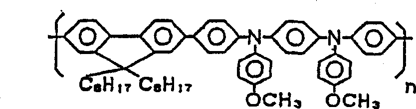

16.按权利要求1~12任一项所述的组合物,其中,前述功能材料是二氧化硅玻璃的前体。16. The composition according to any one of
17.按权利要求1~12任一项所述的组合物,其中,前述功能材料是滤色片用材料。17. The composition according to any one of
18.按权利要求1~17任一项所述的组合物可用于喷墨法。18. A composition as claimed in any one of
19.一种膜的制造方法,其特征在于,将按权利要求1~18任一项所述的组合物供给并分别打在基材上后,再将该基材热处理。19. A method for producing a film, characterized in that the substrate is heat-treated after supplying the composition according to any one of
20.按权利要求19所述的膜的制造方法,在通过喷出装置将前述组合物喷出分别打在基板上后,再将基板在较喷出温度更高的温度下处理。20. According to the method for producing a film according to
21.按权利要求20所述的膜的制造方法,在高温处理时一边加压一边加热。twenty one. According to the method for producing a film according to claim 20, the film is heated while being pressurized during the high-temperature treatment.
22.按权利要求20或21所述的膜的制造方法,在高温处理后原封不动地马上减压除去溶剂。twenty two. In the method for producing a film according to claim 20 or 21, the solvent is removed under reduced pressure immediately after the high-temperature treatment.
23.按权利要求20~22任一项所述的膜的制造方法,其中,前述喷出装置是喷墨印刷装置。twenty three. The method for producing a film according to any one of claims 20 to 22, wherein said ejection means is an inkjet printing means.
24.一种功能元件,其特征在于,它是采用按权利要求1~18任一项所述的组合物形成的。twenty four. A functional element, characterized in that it is formed by using the composition according to any one of claims 1-18.
25.按权利要求24所述的功能元件,其中,前述功能元件是显示元件。25. The functional element according to claim 24, wherein said functional element is a display element.
26.按权利要求25所述的功能元件,其中,前述显示元件,在第一及第二电极之间具备发光材料层,该发光材料层是采用前述组合物所形成构成的。26. The functional device according to claim 25, wherein said display device has a luminescent material layer between the first and second electrodes, and said luminescent material layer is formed using said composition.
27.按权利要求26所述的功能元件,其中,在前述第一电极和前述发光材料层之间,设置正孔注入/输送层。27. The functional element according to claim 26, wherein a positive hole injection/transport layer is provided between said first electrode and said luminescent material layer.
28.按权利要求25~27任一项所述的功能元件,其中,前述显示元件是有机EL元件。28. The functional element according to any one of claims 25 to 27, wherein the display element is an organic EL element.
29.一种功能元件的制造方法,它是按权利要求26所述的功能元件的制造方法,其特征在于,在具有第一电极的基材上,选择性地供给前述组合物,形成发光材料层图形,接着在该发光材料层图形上形成第二电极。29. A method for manufacturing a functional element, which is a method for manufacturing a functional element according to claim 26, characterized in that, on a base material having a first electrode, the aforementioned composition is selectively supplied to form a pattern of a luminescent material layer , and then forming a second electrode on the luminescent material layer pattern.
30.按权利要求29所述的功能元件的制造方法,其中,选择性地供给前述的组合物并热处理形成发光材料层图形。30. A method of manufacturing a functional element according to claim 29, wherein said composition is selectively supplied and heat-treated to form a pattern of a luminescent material layer.
31.按权利要求30所述的功能元件的制造方法,其中,在40℃~200℃的温度范围内进行前述热处理。31. A method of manufacturing a functional element according to claim 30, wherein said heat treatment is performed at a temperature in the range of 40°C to 200°C.
32.按权利要求30或31所述的功能元件的制造方法,其中,在加压下进行前述热处理。32. A method of manufacturing a functional element according to claim 30 or 31, wherein said heat treatment is performed under pressure.
33.按权利要求30~32任一项所述的功能元件的制造方法,其中,对于前述热处理,在组合物完全干燥前减压。33. The method for producing a functional element according to any one of claims 30 to 32, wherein, for the heat treatment, the pressure is reduced before the composition is completely dried.
34.按权利要求29~33任一项所述的功能元件的制造方法,其中,在具有第一电极的前述基材上,采用含有极性溶剂的溶液,在用喷墨法形成正孔注入/输送层之后,在该正孔注入/输送层上,形成前述发光材料层图形,得到有机EL元件。34. The method for manufacturing a functional element according to any one of claims 29 to 33, wherein, on the aforementioned base material having the first electrode, a solution containing a polar solvent is used to form positive holes for injection/transportation by an inkjet method. After layering, on the positive hole injection/transport layer, the pattern of the aforementioned luminescent material layer is formed to obtain an organic EL element.
35.按权利要求29~33任一项所述的功能元件的制造方法,其中,作为前述功能元件,得到有机EL元件。35. The method for producing a functional element according to any one of claims 29 to 33, wherein an organic EL element is obtained as the functional element.
Claims (35)


Applications Claiming Priority (4)
| Application Number | Priority Date | Filing Date | Title |
|---|---|---|---|
| JP86944/1999 | 1999-03-29 | ||
| JP8694499 | 1999-03-29 | ||
| JP250486/1999 | 1999-09-03 | ||
| JP25048699 | 1999-09-03 |
Related Child Applications (2)
| Application Number | Title | Priority Date | Filing Date |
|---|---|---|---|
| CN2008101097047A Division CN101353472B (en) | 1999-03-29 | 2000-03-29 | Composition, film manufacturing method, as well as functional device and manufacturing method therefor |
| CN 200610075547 Division CN1893140B (en) | 1999-03-29 | 2000-03-29 | A film manufacturing method |
Publications (1)
| Publication Number | Publication Date |
|---|---|
| CN1310930A true CN1310930A (en) | 2001-08-29 |
Family
ID=26428022
Family Applications (1)
| Application Number | Title | Priority Date | Filing Date |
|---|---|---|---|
| CN00800987A Pending CN1310930A (en) | 1999-03-29 | 2000-03-29 | Method for producing composition and film, functional element and method for producing same |
Country Status (8)
| Country | Link |
|---|---|
| US (5) | US6878312B1 (en) |
| EP (1) | EP1083775B1 (en) |
| JP (3) | JP4486261B2 (en) |
| KR (1) | KR100495740B1 (en) |
| CN (1) | CN1310930A (en) |
| DE (1) | DE60045092D1 (en) |
| TW (1) | TW508975B (en) |
| WO (1) | WO2000059267A1 (en) |
Cited By (8)
| Publication number | Priority date | Publication date | Assignee | Title |
|---|---|---|---|---|
| CN1618135B (en) * | 2002-01-28 | 2010-05-26 | 摩托罗拉公司 | Semiconductor film and method for manufacturing the same |
| CN101855308A (en) * | 2007-11-16 | 2010-10-06 | 住友化学株式会社 | Coating solution for the coating method in which the coating solution is ejected from a slit-shaped nozzle |
| CN102390174A (en) * | 2010-06-29 | 2012-03-28 | 科迪斯公司 | First drop dissimilarity in drop-on-demand inkjet devices and methods for its correction |
| CN102504803A (en) * | 2011-09-29 | 2012-06-20 | 中国科学院长春应用化学研究所 | Organic luminescent material solution for improving uniformity of inkjet printing films by convection and preparation method thereof |
| CN104508847A (en) * | 2012-06-19 | 2015-04-08 | 剑桥显示技术有限公司 | Method for preparing semiconductor layer |
| CN104908423A (en) * | 2015-06-26 | 2015-09-16 | 京东方科技集团股份有限公司 | Film manufacture method and system thereof |
| WO2017080307A1 (en) * | 2015-11-12 | 2017-05-18 | 广州华睿光电材料有限公司 | Composition for printing electronic devices and application thereof in electronic devices |
| CN107210380A (en) * | 2015-01-26 | 2017-09-26 | 住友化学株式会社 | Composition and the light-emitting component using said composition |
Families Citing this family (131)
| Publication number | Priority date | Publication date | Assignee | Title |
|---|---|---|---|---|
| FR2723831B1 (en) * | 1994-08-25 | 1996-10-25 | Plazanet Maurice | DRIVE DISC FOR THE TOOL OF A MACHINE FOR CONDITIONING AND / OR MAINTENANCE OF FLOORS |
| GB9920543D0 (en) | 1999-08-31 | 1999-11-03 | Cambridge Display Tech Ltd | A formulation for depositing a light-emitting polymer layer |
| US6582504B1 (en) * | 1999-11-24 | 2003-06-24 | Sharp Kabushiki Kaisha | Coating liquid for forming organic EL element |
| EP1309994A2 (en) | 2000-08-18 | 2003-05-14 | Siemens Aktiengesellschaft | Encapsulated organic-electronic component, method for producing the same and use thereof |
| DE60107093T2 (en) | 2000-08-30 | 2005-03-31 | Cambridge Display Technology Ltd. | FORMULATION FOR DEPOSITING A CONJUGATED POLYMER LAYER |
| JP2004105948A (en) * | 2000-11-21 | 2004-04-08 | Seiko Epson Corp | Material discharging method and discharging device, color filter manufacturing method and manufacturing device, liquid crystal device manufacturing method and manufacturing device, EL device manufacturing method and manufacturing device, and electronic equipment |
| JP3628997B2 (en) | 2000-11-27 | 2005-03-16 | セイコーエプソン株式会社 | Method for manufacturing organic electroluminescence device |
| CN1921136B (en) * | 2000-11-27 | 2012-05-09 | 精工爱普生株式会社 | Organic electroluminescent device, and manufacture method thereof |
| JP4021177B2 (en) | 2000-11-28 | 2007-12-12 | セイコーエプソン株式会社 | Organic electroluminescence device manufacturing method, organic electroluminescence device, and electronic apparatus |
| DE10061299A1 (en) | 2000-12-08 | 2002-06-27 | Siemens Ag | Device for determining and / or forwarding at least one environmental influence, production method and use thereof |
| DE10061297C2 (en) | 2000-12-08 | 2003-05-28 | Siemens Ag | Procedure for structuring an OFET |
| TW518909B (en) | 2001-01-17 | 2003-01-21 | Semiconductor Energy Lab | Luminescent device and method of manufacturing same |
| DE10105914C1 (en) | 2001-02-09 | 2002-10-10 | Siemens Ag | Organic field effect transistor with photo-structured gate dielectric and a method for its production |
| US20060082627A9 (en) * | 2001-02-27 | 2006-04-20 | Bright Christopher J | Formulation and method for depositing a material on a substrate |
| TW527432B (en) * | 2001-02-28 | 2003-04-11 | Cambridge Display Tech Ltd | A method and composition for depositing a polymer layer in the production of a light-emissive device, a method of forming a polymer layer on a substrate, and the use of a composition in an ink-jet method of depositing a polymer layer |
| WO2002069119A1 (en) * | 2001-02-27 | 2002-09-06 | Cambridge Display Tech Ltd | Formulation for depositing a material on a substrate using ink jet printing |
| US8232116B2 (en) | 2001-02-28 | 2012-07-31 | Cambridge Display Technology Limited | Method for fabricating a polymer L.E.D. |
| EP1370619B1 (en) * | 2001-03-10 | 2006-06-21 | MERCK PATENT GmbH | Solutions and dispersions of organic semiconductors |
| US6787063B2 (en) * | 2001-03-12 | 2004-09-07 | Seiko Epson Corporation | Compositions, methods for producing films, functional elements, methods for producing functional elements, methods for producing electro-optical devices and methods for producing electronic apparatus |
| JP3969698B2 (en) | 2001-05-21 | 2007-09-05 | 株式会社半導体エネルギー研究所 | Method for manufacturing light emitting device |
| US20020197393A1 (en) * | 2001-06-08 | 2002-12-26 | Hideaki Kuwabara | Process of manufacturing luminescent device |
| DE10135640A1 (en) | 2001-07-21 | 2003-02-06 | Covion Organic Semiconductors | Organic semiconductor solution used for organic integrated switches, organic field effect transistors, organic thin film transistors, organic solar cells and organic laser diodes contains one or more additives |
| US20030166311A1 (en) * | 2001-09-12 | 2003-09-04 | Seiko Epson Corporation | Method for patterning, method for forming film, patterning apparatus, film formation apparatus, electro-optic apparatus and method for manufacturing the same, electronic equipment, and electronic apparatus and method for manufacturing the same |
| DE10151036A1 (en) | 2001-10-16 | 2003-05-08 | Siemens Ag | Isolator for an organic electronic component |
| DE10151440C1 (en) | 2001-10-18 | 2003-02-06 | Siemens Ag | Organic electronic component for implementing an encapsulated partially organic electronic component has components like a flexible foil as an antenna, a diode or capacitor and an organic transistor. |
| DE10153445A1 (en) * | 2001-10-30 | 2003-05-22 | Covion Organic Semiconductors | drying process |
| JP2003163084A (en) * | 2001-11-26 | 2003-06-06 | Seiko Epson Corp | Organic EL device, method of manufacturing the same, and electronic device |
| GB0129005D0 (en) * | 2001-12-04 | 2002-01-23 | Imp College Innovations Ltd | Electroluminescent device |
| JP2005532416A (en) * | 2001-12-20 | 2005-10-27 | アド−ビジョン・インコーポレイテッド | Screen-printable electroluminescent polymer ink |
| KR100817128B1 (en) * | 2001-12-31 | 2008-03-27 | 엘지.필립스 엘시디 주식회사 | Solvent for organic light emitting layer film formation |
| GB0202997D0 (en) * | 2002-02-08 | 2002-03-27 | Elam T Ltd | Method for forming electroluminescent devices |
| KR20020025918A (en) * | 2002-02-15 | 2002-04-04 | 박병주 | Organic semiconducting devices and organic electroluminescent devices produced by using wet process |
| DE10212640B4 (en) | 2002-03-21 | 2004-02-05 | Siemens Ag | Logical components made of organic field effect transistors |
| DE10226370B4 (en) | 2002-06-13 | 2008-12-11 | Polyic Gmbh & Co. Kg | Substrate for an electronic component, use of the substrate, methods for increasing the charge carrier mobility and organic field effect transistor (OFET) |
| US8044517B2 (en) | 2002-07-29 | 2011-10-25 | Polyic Gmbh & Co. Kg | Electronic component comprising predominantly organic functional materials and a method for the production thereof |
| JP4852224B2 (en) * | 2002-07-30 | 2012-01-11 | セイコーエプソン株式会社 | Organic EL device manufacturing equipment |
| JP3690380B2 (en) * | 2002-08-02 | 2005-08-31 | セイコーエプソン株式会社 | Material arrangement method, electronic device manufacturing method, electro-optical device manufacturing method |
| JP4239560B2 (en) | 2002-08-02 | 2009-03-18 | セイコーエプソン株式会社 | Composition and method for producing organic conductive film using the same |
| WO2004023573A2 (en) * | 2002-09-03 | 2004-03-18 | Cambridge Display Technology Limited | Optical device |
| US7368145B2 (en) * | 2002-09-19 | 2008-05-06 | Dai Nippon Printing Co., Ltd. | Method and apparatus for manufacturing organic EL display and color filter by ink jet method |
| JP2011029666A (en) * | 2002-09-30 | 2011-02-10 | Seiko Epson Corp | Application liquid composition and method of forming thin film |
| JP2004179144A (en) * | 2002-09-30 | 2004-06-24 | Seiko Epson Corp | Coating liquid composition and thin film forming method |
| JP4459521B2 (en) | 2002-10-17 | 2010-04-28 | 大日本印刷株式会社 | Electroluminescence display device |
| WO2004043117A1 (en) | 2002-11-07 | 2004-05-21 | Nissan Chemical Industries,Ltd. | Charge-transporting varnish |
| DE10253154A1 (en) | 2002-11-14 | 2004-05-27 | Siemens Ag | Biosensor, used to identify analyte in liquid sample, has test field with detector, where detector registers field changes as electrical signals for evaluation |
| WO2004047144A2 (en) | 2002-11-19 | 2004-06-03 | Polyic Gmbh & Co.Kg | Organic electronic component comprising a structured, semi-conductive functional layer and a method for producing said component |
| GB0227778D0 (en) | 2002-11-28 | 2003-01-08 | Cambridge Display Tech Ltd | Droplet-deposition related methods and apparatus |
| JP4378950B2 (en) * | 2002-12-24 | 2009-12-09 | セイコーエプソン株式会社 | Droplet ejection apparatus and electro-optic device manufacturing method |
| DE10302149A1 (en) | 2003-01-21 | 2005-08-25 | Siemens Ag | Use of conductive carbon black / graphite blends for the production of low-cost electronics |
| JP4131838B2 (en) * | 2003-05-16 | 2008-08-13 | 株式会社半導体エネルギー研究所 | Display device |
| US20040232385A1 (en) | 2003-05-21 | 2004-11-25 | Kram Shari L. | Blend of viscosity modifier and luminescent compound |
| DE10339036A1 (en) | 2003-08-25 | 2005-03-31 | Siemens Ag | Organic electronic component with high-resolution structuring and manufacturing method |
| DE10340643B4 (en) | 2003-09-03 | 2009-04-16 | Polyic Gmbh & Co. Kg | Printing method for producing a double layer for polymer electronics circuits, and thereby produced electronic component with double layer |
| DE10340644B4 (en) | 2003-09-03 | 2010-10-07 | Polyic Gmbh & Co. Kg | Mechanical controls for organic polymer electronics |
| US20050151129A1 (en) * | 2004-01-14 | 2005-07-14 | Rahul Gupta | Deposition of conducting polymers |
| US20070152199A1 (en) * | 2004-03-09 | 2007-07-05 | Arno Seeboth | Composition for the preparation of a thermoset having thermochromic properties |
| JP2005259523A (en) * | 2004-03-11 | 2005-09-22 | Idemitsu Kosan Co Ltd | ORGANIC ELECTROLUMINESCENT DEVICE, ITS MANUFACTURING METHOD, AND ORGANIC SOLUTION |
| JP4247643B2 (en) * | 2004-03-16 | 2009-04-02 | 日産化学工業株式会社 | Antireflective coating containing sulfur atoms |
| US9251923B2 (en) | 2004-04-30 | 2016-02-02 | Nissan Chemical Industries, Ltd. | Varnish containing good solvent and poor solvent |
| WO2005112144A1 (en) * | 2004-05-18 | 2005-11-24 | Merck Patent Gmbh | Formulation for ink-jet printing comprising semiconducting polymers |
| WO2005123856A1 (en) * | 2004-06-17 | 2005-12-29 | Sharp Kabushiki Kaisha | Coating fluid, process for formation of films, processes for production of functional devices, and functional devices |
| DE102004040831A1 (en) | 2004-08-23 | 2006-03-09 | Polyic Gmbh & Co. Kg | Radio-tag compatible outer packaging |
| JP4148933B2 (en) * | 2004-08-31 | 2008-09-10 | シャープ株式会社 | Functional film manufacturing method, functional film forming coating liquid, functional element, electronic device, and display device |
| KR101294902B1 (en) * | 2004-10-15 | 2013-08-08 | 스미또모 가가꾸 가부시키가이샤 | Solution Composition and Polymer Light-Emitting Device |
| DE102004059465A1 (en) | 2004-12-10 | 2006-06-14 | Polyic Gmbh & Co. Kg | recognition system |
| DE102004059464A1 (en) | 2004-12-10 | 2006-06-29 | Polyic Gmbh & Co. Kg | Electronic component with modulator |
| DE102004063435A1 (en) | 2004-12-23 | 2006-07-27 | Polyic Gmbh & Co. Kg | Organic rectifier |
| US8053973B2 (en) * | 2005-02-15 | 2011-11-08 | Pioneer Corporation | Film forming composition and organic electroluminescent device |
| DE102005009820A1 (en) | 2005-03-01 | 2006-09-07 | Polyic Gmbh & Co. Kg | Electronic assembly with organic logic switching elements |
| DE102005009819A1 (en) | 2005-03-01 | 2006-09-07 | Polyic Gmbh & Co. Kg | electronics assembly |
| DE102005017655B4 (en) | 2005-04-15 | 2008-12-11 | Polyic Gmbh & Co. Kg | Multilayer composite body with electronic function |
| GB0510382D0 (en) | 2005-05-20 | 2005-06-29 | Cambridge Display Tech Ltd | Ink jet printing compositions in opto-electrical devices |
| JP2012230904A (en) * | 2005-05-20 | 2012-11-22 | Sumitomo Chemical Co Ltd | High boiling point composition and polymer light emitting element manufactured using the same |
| EP1894976B1 (en) | 2005-05-20 | 2015-09-30 | Sumitomo Chemical Company, Limited | Polymer composition and polymer light-emitting device using same |
| JP4682701B2 (en) * | 2005-05-27 | 2011-05-11 | 凸版印刷株式会社 | Ink for organic EL element and method for producing organic EL element |
| DE102005031448A1 (en) | 2005-07-04 | 2007-01-11 | Polyic Gmbh & Co. Kg | Activatable optical layer |
| DE102005035589A1 (en) | 2005-07-29 | 2007-02-01 | Polyic Gmbh & Co. Kg | Manufacturing electronic component on surface of substrate where component has two overlapping function layers |
| DE102005039528A1 (en) * | 2005-08-18 | 2007-02-22 | Merck Patent Gmbh | Solutions of organic semiconductors |
| GB0517195D0 (en) * | 2005-08-23 | 2005-09-28 | Cambridge Display Tech Ltd | Molecular electronic device structures and fabrication methods |
| WO2007023272A1 (en) | 2005-08-23 | 2007-03-01 | Cambridge Display Technology Limited | Organic electronic device structures and fabrication methods |
| DE102005044306A1 (en) | 2005-09-16 | 2007-03-22 | Polyic Gmbh & Co. Kg | Electronic circuit and method for producing such |
| JP4396607B2 (en) * | 2005-09-28 | 2010-01-13 | セイコーエプソン株式会社 | Film forming method, organic electroluminescent device manufacturing method, organic electroluminescent device, and electronic apparatus |
| CN101331625B (en) * | 2005-10-28 | 2016-03-09 | 日产化学工业株式会社 | Charge transport varnishes for spray or inkjet application |
| JP4251329B2 (en) * | 2005-12-20 | 2009-04-08 | カシオ計算機株式会社 | Display device and manufacturing method thereof |
| GB2437113B (en) * | 2006-04-12 | 2008-11-26 | Cambridge Display Tech Ltd | Light-emissive display and method of manufacturing the same |
| GB0618698D0 (en) * | 2006-09-22 | 2006-11-01 | Cambridge Display Tech Ltd | Molecular electronic device fabrication methods and structures |
| DE102006047388A1 (en) | 2006-10-06 | 2008-04-17 | Polyic Gmbh & Co. Kg | Field effect transistor and electrical circuit |
| GB0803950D0 (en) | 2008-03-03 | 2008-04-09 | Cambridge Display Technology O | Solvent for printing composition |
| GB2462410B (en) | 2008-07-21 | 2011-04-27 | Cambridge Display Tech Ltd | Compositions and methods for manufacturing light-emissive devices |
| GB0814971D0 (en) * | 2008-08-15 | 2008-09-24 | Cambridge Display Tech Ltd | Opto-electrical devices and methods of manufacturing the same |
| GB2462688B (en) | 2008-08-22 | 2012-03-07 | Cambridge Display Tech Ltd | Opto-electrical devices and methods of manufacturing the same |
| GB2463493B (en) | 2008-09-15 | 2012-11-14 | Cambridge Display Tech Ltd | An improved method for ink jet printing organic electronic devices |
| US20110220886A1 (en) * | 2008-09-19 | 2011-09-15 | Idemitsu Kosan Co., Ltd. | Organic electroluminescence material composition, thin film formation method, and organic electroluminescence element |
| US20110226992A1 (en) * | 2008-09-19 | 2011-09-22 | Idemitsu Kosan Co., Ltd. | Organic electroluminescent material compositions |
| GB2466842B (en) * | 2009-01-12 | 2011-10-26 | Cambridge Display Tech Ltd | Interlayer formulation for flat films |
| US8174000B2 (en) | 2009-02-11 | 2012-05-08 | Universal Display Corporation | Liquid compositions for inkjet printing of organic layers or other uses |
| JP2011023668A (en) * | 2009-07-17 | 2011-02-03 | Sumitomo Chemical Co Ltd | Liquid column coating ink, method of manufacturing organic el element, and organic el display device with organic el element |
| KR20130007550A (en) * | 2010-01-13 | 2013-01-18 | 스미또모 가가꾸 가부시키가이샤 | Organic electroluminescent element and light-emitting polymer composition |
| US20130026421A1 (en) | 2010-04-12 | 2013-01-31 | Merck Patent Gmbh | Composition and method for preparation of organic electronic devices |
| GB201013820D0 (en) * | 2010-08-18 | 2010-09-29 | Cambridge Display Tech Ltd | Low contact resistance organic thin film transistors |
| JP5527105B2 (en) * | 2010-08-24 | 2014-06-18 | セイコーエプソン株式会社 | Film forming ink, film forming method, and light emitting element manufacturing method |
| JP5527104B2 (en) * | 2010-08-24 | 2014-06-18 | セイコーエプソン株式会社 | Film forming ink, film forming method, and light emitting element manufacturing method |
| US8956740B2 (en) | 2010-08-24 | 2015-02-17 | Seiko Epson Corporation | Film-forming ink, film-forming method, liquid droplet discharging device, method for preparing light-emitting element, light-emitting element, light-emitting device and electronic apparatus |
| KR101827975B1 (en) | 2011-10-10 | 2018-03-29 | 엘지이노텍 주식회사 | Light emitting device |
| KR101389451B1 (en) * | 2012-03-19 | 2014-04-29 | 연세대학교 산학협력단 | Composition for oxide thin film, Method for forming oxide thin film, an electrical device using the low-temperature pressure annealing, and a thin film transistor |
| JP6015073B2 (en) * | 2012-04-02 | 2016-10-26 | セイコーエプソン株式会社 | Functional layer forming ink and light emitting device manufacturing method |
| US20130314327A1 (en) * | 2012-05-22 | 2013-11-28 | J Touch Corporation | Frameless touch panel |
| DE102012018583B4 (en) | 2012-09-20 | 2018-10-31 | Heidelberger Druckmaschinen Ag | Method for printing a functional layer for electronic components |
| JP6079118B2 (en) * | 2012-10-10 | 2017-02-15 | コニカミノルタ株式会社 | Light-emitting layer forming ink composition, method for producing light-emitting element, and electroluminescence device |
| JP6214938B2 (en) * | 2013-06-18 | 2017-10-18 | 日本化薬株式会社 | Organic semiconductor and its use, and semiconductor layer forming ink |
| CN105431910B (en) | 2013-08-12 | 2018-03-06 | 科迪华公司 | Ester-based solvent systems for printable organic light-emitting diode ink formulations |
| KR102145424B1 (en) * | 2013-11-11 | 2020-08-18 | 엘지디스플레이 주식회사 | Ink for display device manufacturing and method for manufacturing of the same, method for manufacturing using the same |
| JP6551238B2 (en) | 2014-02-14 | 2019-07-31 | 日立化成株式会社 | Polymer or oligomer, hole transport material composition, and organic electronic device using the same |
| WO2015194429A1 (en) * | 2014-06-17 | 2015-12-23 | 株式会社ダイセル | Solvent for manufacturing organic el elements |
| US10020185B2 (en) | 2014-10-07 | 2018-07-10 | Samsung Sdi Co., Ltd. | Composition for forming silica layer, silica layer, and electronic device |
| JP6638187B2 (en) * | 2014-12-02 | 2020-01-29 | セイコーエプソン株式会社 | Film forming ink and film forming method |
| JP6638186B2 (en) * | 2014-12-02 | 2020-01-29 | セイコーエプソン株式会社 | Film forming ink and film forming method |
| KR101837971B1 (en) | 2014-12-19 | 2018-03-13 | 삼성에스디아이 주식회사 | Composition for forming silica based layer, silica based layer, and electronic device |
| KR101833800B1 (en) | 2014-12-19 | 2018-03-02 | 삼성에스디아이 주식회사 | Composition for forming silica based layer, method for manufacturing silica based layer, and electronic device including the silica based layer |
| US10756269B2 (en) | 2015-03-05 | 2020-08-25 | Sumitomo Chemical Company, Limited | Composition and light emitting device using the same |
| KR102386848B1 (en) | 2015-04-13 | 2022-04-15 | 삼성디스플레이 주식회사 | Display device and method of manufacturing the same |
| WO2016186012A1 (en) * | 2015-05-19 | 2016-11-24 | 住友化学株式会社 | Composition and light-emitting element in which same is used |
| KR20170014946A (en) * | 2015-07-31 | 2017-02-08 | 삼성에스디아이 주식회사 | Composition for forming silica layer, method for manufacturing silica layer, and silica layer |
| EP3390549B1 (en) * | 2015-12-16 | 2022-06-29 | Merck Patent GmbH | Formulations containing a solid solvent |
| JP6661365B2 (en) * | 2015-12-17 | 2020-03-11 | 東芝テック株式会社 | Method and apparatus for manufacturing ink-jet ink and organic thin-film solar cell |
| JP6833388B2 (en) * | 2016-08-01 | 2021-02-24 | 株式会社Joled | Ink for organic EL |
| CN109790407B (en) | 2016-11-23 | 2021-12-07 | 广州华睿光电材料有限公司 | Printing ink composition, preparation method and application thereof |
| TWI763772B (en) * | 2017-01-30 | 2022-05-11 | 德商麥克專利有限公司 | Method for forming an organic element of an electronic device |
| WO2020094538A1 (en) * | 2018-11-06 | 2020-05-14 | Merck Patent Gmbh | Method for forming an organic element of an electronic device |
| CN111876020B (en) * | 2020-08-06 | 2021-11-05 | 中国科学院长春应用化学研究所 | Organic luminescent material ink, preparation method thereof and ink-jet printing method |
| WO2024024508A1 (en) * | 2022-07-25 | 2024-02-01 | 富士フイルム株式会社 | Composition, film, optical filter, solid state imaging device, image display device, infrared radiation sensor, and method for producing camera module |
Family Cites Families (58)
| Publication number | Priority date | Publication date | Assignee | Title |
|---|---|---|---|---|
| DE927152C (en) | 1952-02-23 | 1955-05-02 | Huels Chemische Werke Ag | Printing pastes |
| US4378302A (en) * | 1980-12-16 | 1983-03-29 | General Electric Company | Red perylene dichroic dye containing liquid crystal formulations |
| JPS5964678A (en) * | 1982-10-04 | 1984-04-12 | Nippon Telegr & Teleph Corp <Ntt> | Ink for ink jet recording |
| JPS5971372A (en) * | 1982-10-15 | 1984-04-23 | Oki Electric Ind Co Ltd | Ink for ink jet |
| US4713198A (en) * | 1984-04-27 | 1987-12-15 | Sangamo Weston, Inc. | High temperature plastic scintillators |
| JPS62243285A (en) | 1986-04-14 | 1987-10-23 | 松下電器産業株式会社 | Electroluminescent panel and method for forming the same |
| JPS62292871A (en) * | 1986-06-13 | 1987-12-19 | Fuji Xerox Co Ltd | Recording composition |
| JPS63264684A (en) * | 1986-12-05 | 1988-11-01 | Dainippon Ink & Chem Inc | Ink composition |
| JPS6416880A (en) * | 1987-07-10 | 1989-01-20 | Fuji Photo Film Co Ltd | Recording liquid |
| US5091004A (en) | 1987-09-22 | 1992-02-25 | Dainippon Ink And Chemicals, Inc. | Ink composition |
| JPH01161350A (en) * | 1987-12-18 | 1989-06-26 | Konica Corp | Printing method using planographic printing plate |
| US5006370A (en) * | 1988-10-11 | 1991-04-09 | Ethyl Corporation | Compositions for production of electronic coatings |
| US5068131A (en) * | 1988-10-11 | 1991-11-26 | Ethyl Corporation | Method for production of electronic coatings |
| US4855120A (en) * | 1988-10-24 | 1989-08-08 | Ethyl Corporation | Production of silane and useful coproducts |
| DE3934329A1 (en) * | 1989-10-13 | 1991-04-18 | Basf Ag | POLYMERIZABLE PERYLENE-3,4,9,10-TETRACARBONE ACID BISIMIDES AND THEIR POLYMERISATES |
| JPH04153280A (en) * | 1990-10-16 | 1992-05-26 | Seiko Epson Corp | Inkjet recording ink |
| US5443922A (en) * | 1991-11-07 | 1995-08-22 | Konica Corporation | Organic thin film electroluminescence element |
| JPH05224008A (en) * | 1992-02-13 | 1993-09-03 | Toray Ind Inc | Color filter |
| AU661382B2 (en) * | 1992-04-02 | 1995-07-20 | Nippon Paper Industries Co. Ltd. | Novel bis-dithiobenzilnickel complexes and benzoin derivatives |
| JPH069910A (en) * | 1992-06-26 | 1994-01-18 | Seiko Epson Corp | Ink composition |
| JP3644458B2 (en) * | 1995-02-13 | 2005-04-27 | ソニー株式会社 | Recording method and recording liquid |
| JP3036436B2 (en) | 1996-06-19 | 2000-04-24 | セイコーエプソン株式会社 | Method of manufacturing active matrix type organic EL display |
| US6207301B1 (en) * | 1996-08-21 | 2001-03-27 | Sumitomo Chemical Company, Limited | Polymer fluorescent substance and organic electroluminescence device |
| JP3899566B2 (en) | 1996-11-25 | 2007-03-28 | セイコーエプソン株式会社 | Manufacturing method of organic EL display device |
| JPH10321369A (en) | 1997-03-19 | 1998-12-04 | Fuji Photo Film Co Ltd | Electroluminescent device |
| DE69831990T2 (en) | 1997-03-19 | 2006-05-24 | Fuji Photo Film Co., Ltd., Minami-Ashigara | Electroluminescent device |
| JP3415741B2 (en) * | 1997-03-31 | 2003-06-09 | 東レ・ダウコーニング・シリコーン株式会社 | Composition for forming electrically insulating thin film and method for forming electrically insulating thin film |
| US6309763B1 (en) * | 1997-05-21 | 2001-10-30 | The Dow Chemical Company | Fluorene-containing polymers and electroluminescent devices therefrom |
| US5998045A (en) * | 1997-07-03 | 1999-12-07 | International Business Machines Corporation | Polymeric light-emitting device |
| US6843937B1 (en) * | 1997-07-16 | 2005-01-18 | Seiko Epson Corporation | Composition for an organic EL element and method of manufacturing the organic EL element |
| JP3911775B2 (en) | 1997-07-30 | 2007-05-09 | セイコーエプソン株式会社 | Manufacturing method of organic EL element |
| JPH1154272A (en) * | 1997-07-31 | 1999-02-26 | Seiko Epson Corp | Method of manufacturing light emitting display |
| DE69834395T2 (en) | 1997-09-02 | 2007-02-08 | Seiko Epson Corp. | METHOD FOR PRODUCING AN ORGANIC ELECTROLUMINESCENT DEVICE |
| US6403236B1 (en) * | 1997-09-04 | 2002-06-11 | Sumitomo Chemical Company, Limited | Polymer light emitting device |
| US6497969B2 (en) * | 1997-09-05 | 2002-12-24 | Nessdisplay Co., Ltd. | Electroluminescent device having an organic layer including polyimide |
| EP1010360B1 (en) | 1997-09-05 | 2004-03-17 | Cambridge Display Technology Limited | SELF-ASSEMBLED TRANSPORT LAYERS FOR OLEDs |
| ATE434259T1 (en) | 1997-10-14 | 2009-07-15 | Patterning Technologies Ltd | METHOD OF MAKING AN ELECTRICAL CAPACITOR |
| US5777070A (en) * | 1997-10-23 | 1998-07-07 | The Dow Chemical Company | Process for preparing conjugated polymers |
| JP3104223B2 (en) * | 1997-11-06 | 2000-10-30 | 日本電気株式会社 | Organic electroluminescent device |
| WO1999048337A1 (en) | 1998-03-13 | 1999-09-23 | Cambridge Display Technology Ltd. | Electroluminescent devices |
| US6403237B1 (en) * | 1998-06-10 | 2002-06-11 | Sumitomo Chemical Co., Ltd. | Polymeric fluorescent substance and organic electroluminescence device |
| JP3823602B2 (en) | 1998-06-10 | 2006-09-20 | 住友化学株式会社 | Polymer fluorescent substance and organic electroluminescence device |
| JP2000077187A (en) * | 1998-06-17 | 2000-03-14 | Honda Motor Co Ltd | Organic electroluminescence device |
| JP3900724B2 (en) * | 1999-01-11 | 2007-04-04 | セイコーエプソン株式会社 | Organic EL element manufacturing method and organic EL display device |
| US6228228B1 (en) * | 1999-02-23 | 2001-05-08 | Sarnoff Corporation | Method of making a light-emitting fiber |
| GB9917356D0 (en) | 1999-07-24 | 1999-09-22 | Univ Cambridge Tech | Aromatic monomers and polymers for optoelectronic devices |
| GB9920543D0 (en) | 1999-08-31 | 1999-11-03 | Cambridge Display Tech Ltd | A formulation for depositing a light-emitting polymer layer |
| JP2001076880A (en) * | 1999-08-31 | 2001-03-23 | Sumitomo Chem Co Ltd | Organic electroluminescence device |
| WO2001017319A1 (en) * | 1999-09-01 | 2001-03-08 | Osram Opto Semiconductors Gmbh & Co. Ohg | Organic electroluminescent device and production method |
| GB2360489A (en) * | 2000-03-23 | 2001-09-26 | Seiko Epson Corp | Deposition of soluble materials |
| US20060082627A9 (en) * | 2001-02-27 | 2006-04-20 | Bright Christopher J | Formulation and method for depositing a material on a substrate |
| WO2002069119A1 (en) * | 2001-02-27 | 2002-09-06 | Cambridge Display Tech Ltd | Formulation for depositing a material on a substrate using ink jet printing |
| JP4153280B2 (en) | 2002-09-27 | 2008-09-24 | シャープ株式会社 | Optical pickup device |
| DE102004007777A1 (en) * | 2004-02-18 | 2005-09-08 | Covion Organic Semiconductors Gmbh | Solutions of organic semiconductors |
| DE102004023276A1 (en) * | 2004-05-11 | 2005-12-01 | Covion Organic Semiconductors Gmbh | Solutions of organic semiconductors |
| JP5228341B2 (en) * | 2007-03-14 | 2013-07-03 | セイコーエプソン株式会社 | Method for manufacturing organic electroluminescence element and method for manufacturing organic transistor |
| WO2012001744A1 (en) * | 2010-07-01 | 2012-01-05 | パナソニック株式会社 | Ink for organic light emitting element, method for manufacturing organic light emitting element, organic display panel, organic display device, organic light emitting device, ink, method for forming functional layer, and organic light emitting element |
| JP2012028180A (en) * | 2010-07-23 | 2012-02-09 | Panasonic Corp | Method and apparatus for manufacturing display device |
-
2000
- 2000-03-29 CN CN00800987A patent/CN1310930A/en active Pending
- 2000-03-29 DE DE60045092T patent/DE60045092D1/en not_active Expired - Lifetime
- 2000-03-29 EP EP00912924A patent/EP1083775B1/en not_active Expired - Lifetime
- 2000-03-29 JP JP2000608851A patent/JP4486261B2/en not_active Expired - Lifetime
- 2000-03-29 WO PCT/JP2000/001962 patent/WO2000059267A1/en not_active Ceased
- 2000-03-29 TW TW89105849A patent/TW508975B/en not_active IP Right Cessation
- 2000-03-29 US US09/701,468 patent/US6878312B1/en not_active Expired - Lifetime
- 2000-03-29 KR KR10-2000-7013448A patent/KR100495740B1/en not_active Expired - Lifetime
-
2005
- 2005-03-11 US US11/077,087 patent/US20050156148A1/en not_active Abandoned
-
2008
- 2008-08-04 US US12/222,165 patent/US8231932B2/en not_active Expired - Fee Related
-
2009
- 2009-03-10 US US12/382,161 patent/US8187669B2/en not_active Expired - Fee Related
-
2010
- 2010-02-12 JP JP2010028943A patent/JP4731629B2/en not_active Expired - Lifetime
- 2010-09-24 JP JP2010213030A patent/JP5286339B2/en not_active Expired - Lifetime
-
2012
- 2012-06-29 US US13/538,010 patent/US9620719B2/en not_active Expired - Fee Related
Cited By (16)
| Publication number | Priority date | Publication date | Assignee | Title |
|---|---|---|---|---|
| CN1618135B (en) * | 2002-01-28 | 2010-05-26 | 摩托罗拉公司 | Semiconductor film and method for manufacturing the same |
| CN101855308A (en) * | 2007-11-16 | 2010-10-06 | 住友化学株式会社 | Coating solution for the coating method in which the coating solution is ejected from a slit-shaped nozzle |
| CN102390174A (en) * | 2010-06-29 | 2012-03-28 | 科迪斯公司 | First drop dissimilarity in drop-on-demand inkjet devices and methods for its correction |
| US10744759B2 (en) | 2010-06-29 | 2020-08-18 | CARDINAL HEALTH SWITZERLAND 515 GmbH | First drop dissimilarity in drop-on-demand inkjet devices and methods for its correction |
| CN102504803A (en) * | 2011-09-29 | 2012-06-20 | 中国科学院长春应用化学研究所 | Organic luminescent material solution for improving uniformity of inkjet printing films by convection and preparation method thereof |
| CN102504803B (en) * | 2011-09-29 | 2013-11-27 | 中国科学院长春应用化学研究所 | A kind of organic light-emitting material solution and its preparation method for improving the uniformity of inkjet printing film by using convection |
| TWI607998B (en) * | 2012-06-19 | 2017-12-11 | 劍橋顯示科技有限公司 | method |
| CN104508847A (en) * | 2012-06-19 | 2015-04-08 | 剑桥显示技术有限公司 | Method for preparing semiconductor layer |
| CN104508847B (en) * | 2012-06-19 | 2018-02-13 | 剑桥显示技术有限公司 | Method for preparing semiconductor layer |
| CN107210380A (en) * | 2015-01-26 | 2017-09-26 | 住友化学株式会社 | Composition and the light-emitting component using said composition |
| CN107210380B (en) * | 2015-01-26 | 2019-06-28 | 住友化学株式会社 | Composition and light-emitting element using the same |
| US10323181B2 (en) | 2015-01-26 | 2019-06-18 | Sumitomo Chemical Company, Limited | Composition containing phosphorescent compound and light emitting device using the same |
| CN104908423B (en) * | 2015-06-26 | 2016-08-24 | 京东方科技集团股份有限公司 | A kind of film manufacturing method and system |
| CN104908423A (en) * | 2015-06-26 | 2015-09-16 | 京东方科技集团股份有限公司 | Film manufacture method and system thereof |
| WO2017080307A1 (en) * | 2015-11-12 | 2017-05-18 | 广州华睿光电材料有限公司 | Composition for printing electronic devices and application thereof in electronic devices |
| CN108291105A (en) * | 2015-11-12 | 2018-07-17 | 广州华睿光电材料有限公司 | Application for the composition of printed electronic device and its in electronic device |
Also Published As
| Publication number | Publication date |
|---|---|
| US20050156148A1 (en) | 2005-07-21 |
| TW508975B (en) | 2002-11-01 |
| HK1128714A1 (en) | 2009-11-06 |
| JP2010157751A (en) | 2010-07-15 |
| JP2011042794A (en) | 2011-03-03 |
| US20120263867A1 (en) | 2012-10-18 |
| US20090186161A1 (en) | 2009-07-23 |
| KR20010043918A (en) | 2001-05-25 |
| US8231932B2 (en) | 2012-07-31 |
| JP5286339B2 (en) | 2013-09-11 |
| KR100495740B1 (en) | 2005-06-17 |
| JP4486261B2 (en) | 2010-06-23 |
| DE60045092D1 (en) | 2010-11-25 |
| US6878312B1 (en) | 2005-04-12 |
| US20080305245A1 (en) | 2008-12-11 |
| US8187669B2 (en) | 2012-05-29 |
| WO2000059267A1 (en) | 2000-10-05 |
| US9620719B2 (en) | 2017-04-11 |
| EP1083775A4 (en) | 2005-12-07 |
| JP4731629B2 (en) | 2011-07-27 |
| EP1083775B1 (en) | 2010-10-13 |
| EP1083775A1 (en) | 2001-03-14 |
Similar Documents
| Publication | Publication Date | Title |
|---|---|---|
| CN1310930A (en) | Method for producing composition and film, functional element and method for producing same | |
| CN1199520C (en) | Organic electroluminescence device, its manufacturing method, and electronic device | |
| Jiang et al. | Full-color quantum dots active matrix display fabricated by ink-jet printing | |
| CN1922744A (en) | Solutions of organic semiconductors | |
| CN1138458C (en) | Organic electroluminescent element, method for manufacturing the same, and organic electroluminescent display device | |
| JPWO2000059267A1 (en) | Composition, film manufacturing method, functional element and manufacturing method thereof | |
| CN1481204A (en) | Composition, organic conductive film using same, and method for producing same | |
| CN1736130A (en) | Manufacturing method of light emitting device | |
| CN1741693A (en) | Method of manufacturing electron device and organic electroluminescent display and ink for organic amorphous film | |
| CN1653855A (en) | Production method for electroluminescent element | |
| CN1444427A (en) | Light emitting device and manufacturing method thereof | |
| CN1822384A (en) | Semiconductor device and manufacturing method thereof | |
| CN1879237A (en) | Process for forming organic layers with a region including a guest material and organic electronic devices incorporating the same | |
| Bail et al. | Inkjet printing of blue phosphorescent light-emitting layer based on bis (3, 5-di (9 H-carbazol-9-yl)) diphenylsilane | |
| WO2007004627A1 (en) | Patterning apparatus, organic electroluminescence element, method for manufacturing such organic electroluminescence element, and organic electroluminescence display device | |
| CN1496197A (en) | Method for producing image element, equipment for producing image element and image element | |
| CN1893140A (en) | A film manufacturing method | |
| WO2022078429A1 (en) | Light-emitting device and use thereof in display | |
| CN110643223A (en) | Ink for ink-jet printing organic light-emitting layer and preparation method and application thereof | |
| CN1575072A (en) | Providing an emission-protecting layer in an OLED device | |
| CN1703122A (en) | Method of manufacturing color filter substrate, method of manufacturing electro-optical device, electro-optical device, and electronic apparatus | |
| CN111704829A (en) | Polymer thermally activated delayed fluorescent material ink for inkjet printing, its preparation method and inkjet printing method | |
| Hu et al. | High-Performance Inkjet Printed OLEDs Realized by Improved Film Morphology | |
| KR101678282B1 (en) | Composition for removing materials in via-hole, method for removing materials in via-hole and method for manufacturing top emission oled panel using the same | |
| CN114551737A (en) | Method for forming hole injection layer and hole injection layer ink composition |
Legal Events
| Date | Code | Title | Description |
|---|---|---|---|
| C06 | Publication | ||
| PB01 | Publication | ||
| C10 | Entry into substantive examination | ||
| SE01 | Entry into force of request for substantive examination | ||
| ASS | Succession or assignment of patent right |
Owner name: CAMBRIDGE DISPLAY TECHNOLOGY LTD. Effective date: 20020614 |
|
| C41 | Transfer of patent application or patent right or utility model | ||
| TA01 | Transfer of patent application right |
Effective date of registration: 20020614 Address after: Tokyo, Japan, Japan Applicant after: Seiko Epson Corp. Co-applicant after: Camgridge Display Technology Ltd. Address before: Tokyo, Japan, Japan Applicant before: Seiko Epson Corp. |