CN1248307C - Semiconductor device and its producing method - Google Patents
Semiconductor device and its producing method Download PDFInfo
- Publication number
- CN1248307C CN1248307C CNB02132123XA CN02132123A CN1248307C CN 1248307 C CN1248307 C CN 1248307C CN B02132123X A CNB02132123X A CN B02132123XA CN 02132123 A CN02132123 A CN 02132123A CN 1248307 C CN1248307 C CN 1248307C
- Authority
- CN
- China
- Prior art keywords
- substrate
- resin
- aforementioned
- semiconductor device
- mold
- Prior art date
- Legal status (The legal status is an assumption and is not a legal conclusion. Google has not performed a legal analysis and makes no representation as to the accuracy of the status listed.)
- Expired - Lifetime
Links
- 239000004065 semiconductor Substances 0.000 title claims abstract description 56
- 238000000034 method Methods 0.000 title claims description 23
- 239000000758 substrate Substances 0.000 claims abstract description 156
- 229920005989 resin Polymers 0.000 claims abstract description 140
- 239000011347 resin Substances 0.000 claims abstract description 140
- 239000002184 metal Substances 0.000 claims abstract description 94
- 239000000919 ceramic Substances 0.000 claims abstract description 55
- 238000007789 sealing Methods 0.000 claims abstract description 53
- 238000004519 manufacturing process Methods 0.000 claims abstract description 26
- 239000000853 adhesive Substances 0.000 claims abstract description 14
- 230000001070 adhesive effect Effects 0.000 claims abstract description 14
- 229920001971 elastomer Polymers 0.000 claims description 36
- 229920002379 silicone rubber Polymers 0.000 claims description 4
- 239000004945 silicone rubber Substances 0.000 claims description 4
- 238000009751 slip forming Methods 0.000 claims description 2
- 239000003822 epoxy resin Substances 0.000 abstract description 35
- 229920000647 polyepoxide Polymers 0.000 abstract description 35
- ZUOUZKKEUPVFJK-UHFFFAOYSA-N diphenyl Chemical compound C1=CC=CC=C1C1=CC=CC=C1 ZUOUZKKEUPVFJK-UHFFFAOYSA-N 0.000 description 10
- 238000001721 transfer moulding Methods 0.000 description 10
- 238000005520 cutting process Methods 0.000 description 9
- 239000000428 dust Substances 0.000 description 9
- 230000002093 peripheral effect Effects 0.000 description 9
- 238000007639 printing Methods 0.000 description 8
- 230000008569 process Effects 0.000 description 8
- 230000000694 effects Effects 0.000 description 7
- 238000002347 injection Methods 0.000 description 7
- 239000007924 injection Substances 0.000 description 7
- -1 glycidyl ester Chemical class 0.000 description 6
- 238000000465 moulding Methods 0.000 description 6
- 229920000139 polyethylene terephthalate Polymers 0.000 description 6
- 239000005020 polyethylene terephthalate Substances 0.000 description 6
- PNEYBMLMFCGWSK-UHFFFAOYSA-N aluminium oxide Inorganic materials [O-2].[O-2].[O-2].[Al+3].[Al+3] PNEYBMLMFCGWSK-UHFFFAOYSA-N 0.000 description 5
- 235000010290 biphenyl Nutrition 0.000 description 5
- 239000004305 biphenyl Substances 0.000 description 5
- 239000003990 capacitor Substances 0.000 description 5
- 238000005336 cracking Methods 0.000 description 5
- 238000010586 diagram Methods 0.000 description 5
- 239000000126 substance Substances 0.000 description 5
- 238000007664 blowing Methods 0.000 description 4
- 229920003986 novolac Polymers 0.000 description 4
- 230000002787 reinforcement Effects 0.000 description 4
- LYCAIKOWRPUZTN-UHFFFAOYSA-N Ethylene glycol Chemical compound OCCO LYCAIKOWRPUZTN-UHFFFAOYSA-N 0.000 description 3
- 239000004952 Polyamide Substances 0.000 description 3
- LNEPOXFFQSENCJ-UHFFFAOYSA-N haloperidol Chemical compound C1CC(O)(C=2C=CC(Cl)=CC=2)CCN1CCCC(=O)C1=CC=C(F)C=C1 LNEPOXFFQSENCJ-UHFFFAOYSA-N 0.000 description 3
- 239000011159 matrix material Substances 0.000 description 3
- 229920002647 polyamide Polymers 0.000 description 3
- 238000003672 processing method Methods 0.000 description 3
- 229920002050 silicone resin Polymers 0.000 description 3
- 238000005245 sintering Methods 0.000 description 3
- 229910001220 stainless steel Inorganic materials 0.000 description 3
- 239000010935 stainless steel Substances 0.000 description 3
- 230000037303 wrinkles Effects 0.000 description 3
- QTWJRLJHJPIABL-UHFFFAOYSA-N 2-methylphenol;3-methylphenol;4-methylphenol Chemical compound CC1=CC=C(O)C=C1.CC1=CC=CC(O)=C1.CC1=CC=CC=C1O QTWJRLJHJPIABL-UHFFFAOYSA-N 0.000 description 2
- FVCSARBUZVPSQF-UHFFFAOYSA-N 5-(2,4-dioxooxolan-3-yl)-7-methyl-3a,4,5,7a-tetrahydro-2-benzofuran-1,3-dione Chemical compound C1C(C(OC2=O)=O)C2C(C)=CC1C1C(=O)COC1=O FVCSARBUZVPSQF-UHFFFAOYSA-N 0.000 description 2
- 229920002799 BoPET Polymers 0.000 description 2
- 239000002033 PVDF binder Substances 0.000 description 2
- ISWSIDIOOBJBQZ-UHFFFAOYSA-N Phenol Chemical compound OC1=CC=CC=C1 ISWSIDIOOBJBQZ-UHFFFAOYSA-N 0.000 description 2
- 239000004734 Polyphenylene sulfide Substances 0.000 description 2
- 125000002619 bicyclic group Chemical group 0.000 description 2
- 230000008859 change Effects 0.000 description 2
- 238000007796 conventional method Methods 0.000 description 2
- 229920001577 copolymer Polymers 0.000 description 2
- 229930003836 cresol Natural products 0.000 description 2
- 239000004850 liquid epoxy resins (LERs) Substances 0.000 description 2
- 239000000463 material Substances 0.000 description 2
- 229920002493 poly(chlorotrifluoroethylene) Polymers 0.000 description 2
- 239000005023 polychlorotrifluoroethylene (PCTFE) polymer Substances 0.000 description 2
- 229920000069 polyphenylene sulfide Polymers 0.000 description 2
- 229920001343 polytetrafluoroethylene Polymers 0.000 description 2
- 239000004810 polytetrafluoroethylene Substances 0.000 description 2
- 229920002981 polyvinylidene fluoride Polymers 0.000 description 2
- 239000011148 porous material Substances 0.000 description 2
- 238000003825 pressing Methods 0.000 description 2
- FBOUIAKEJMZPQG-AWNIVKPZSA-N (1E)-1-(2,4-dichlorophenyl)-4,4-dimethyl-2-(1,2,4-triazol-1-yl)pent-1-en-3-ol Chemical compound C1=NC=NN1/C(C(O)C(C)(C)C)=C/C1=CC=C(Cl)C=C1Cl FBOUIAKEJMZPQG-AWNIVKPZSA-N 0.000 description 1
- 230000001154 acute effect Effects 0.000 description 1
- 125000002723 alicyclic group Chemical group 0.000 description 1
- 238000005452 bending Methods 0.000 description 1
- 238000005266 casting Methods 0.000 description 1
- 239000011248 coating agent Substances 0.000 description 1
- 238000000576 coating method Methods 0.000 description 1
- GYZLOYUZLJXAJU-UHFFFAOYSA-N diglycidyl ether Chemical compound C1OC1COCC1CO1 GYZLOYUZLJXAJU-UHFFFAOYSA-N 0.000 description 1
- 238000005538 encapsulation Methods 0.000 description 1
- 229920000840 ethylene tetrafluoroethylene copolymer Polymers 0.000 description 1
- 230000006872 improvement Effects 0.000 description 1
- 230000007246 mechanism Effects 0.000 description 1
- 239000000203 mixture Substances 0.000 description 1
- 238000012986 modification Methods 0.000 description 1
- 230000004048 modification Effects 0.000 description 1
- RXOHFPCZGPKIRD-UHFFFAOYSA-N naphthalene-2,6-dicarboxylic acid Chemical compound C1=C(C(O)=O)C=CC2=CC(C(=O)O)=CC=C21 RXOHFPCZGPKIRD-UHFFFAOYSA-N 0.000 description 1
- 239000004843 novolac epoxy resin Substances 0.000 description 1
- AFEQENGXSMURHA-UHFFFAOYSA-N oxiran-2-ylmethanamine Chemical compound NCC1CO1 AFEQENGXSMURHA-UHFFFAOYSA-N 0.000 description 1
- 238000004806 packaging method and process Methods 0.000 description 1
- 238000012856 packing Methods 0.000 description 1
- 239000003566 sealing material Substances 0.000 description 1
Images


Classifications
-
- H—ELECTRICITY
- H01—ELECTRIC ELEMENTS
- H01L—SEMICONDUCTOR DEVICES NOT COVERED BY CLASS H10
- H01L23/00—Details of semiconductor or other solid state devices
- H01L23/12—Mountings, e.g. non-detachable insulating substrates
-
- H—ELECTRICITY
- H01—ELECTRIC ELEMENTS
- H01L—SEMICONDUCTOR DEVICES NOT COVERED BY CLASS H10
- H01L21/00—Processes or apparatus adapted for the manufacture or treatment of semiconductor or solid state devices or of parts thereof
- H01L21/02—Manufacture or treatment of semiconductor devices or of parts thereof
- H01L21/04—Manufacture or treatment of semiconductor devices or of parts thereof the devices having potential barriers, e.g. a PN junction, depletion layer or carrier concentration layer
- H01L21/50—Assembly of semiconductor devices using processes or apparatus not provided for in a single one of the groups H01L21/18 - H01L21/326 or H10D48/04 - H10D48/07 e.g. sealing of a cap to a base of a container
- H01L21/56—Encapsulations, e.g. encapsulation layers, coatings
- H01L21/561—Batch processing
-
- H—ELECTRICITY
- H01—ELECTRIC ELEMENTS
- H01L—SEMICONDUCTOR DEVICES NOT COVERED BY CLASS H10
- H01L21/00—Processes or apparatus adapted for the manufacture or treatment of semiconductor or solid state devices or of parts thereof
- H01L21/02—Manufacture or treatment of semiconductor devices or of parts thereof
- H01L21/04—Manufacture or treatment of semiconductor devices or of parts thereof the devices having potential barriers, e.g. a PN junction, depletion layer or carrier concentration layer
- H01L21/50—Assembly of semiconductor devices using processes or apparatus not provided for in a single one of the groups H01L21/18 - H01L21/326 or H10D48/04 - H10D48/07 e.g. sealing of a cap to a base of a container
- H01L21/56—Encapsulations, e.g. encapsulation layers, coatings
- H01L21/565—Moulds
-
- H—ELECTRICITY
- H01—ELECTRIC ELEMENTS
- H01L—SEMICONDUCTOR DEVICES NOT COVERED BY CLASS H10
- H01L21/00—Processes or apparatus adapted for the manufacture or treatment of semiconductor or solid state devices or of parts thereof
- H01L21/02—Manufacture or treatment of semiconductor devices or of parts thereof
- H01L21/04—Manufacture or treatment of semiconductor devices or of parts thereof the devices having potential barriers, e.g. a PN junction, depletion layer or carrier concentration layer
- H01L21/50—Assembly of semiconductor devices using processes or apparatus not provided for in a single one of the groups H01L21/18 - H01L21/326 or H10D48/04 - H10D48/07 e.g. sealing of a cap to a base of a container
- H01L21/56—Encapsulations, e.g. encapsulation layers, coatings
- H01L21/568—Temporary substrate used as encapsulation process aid
-
- H—ELECTRICITY
- H01—ELECTRIC ELEMENTS
- H01L—SEMICONDUCTOR DEVICES NOT COVERED BY CLASS H10
- H01L23/00—Details of semiconductor or other solid state devices
- H01L23/28—Encapsulations, e.g. encapsulating layers, coatings, e.g. for protection
- H01L23/31—Encapsulations, e.g. encapsulating layers, coatings, e.g. for protection characterised by the arrangement or shape
- H01L23/3107—Encapsulations, e.g. encapsulating layers, coatings, e.g. for protection characterised by the arrangement or shape the device being completely enclosed
- H01L23/3121—Encapsulations, e.g. encapsulating layers, coatings, e.g. for protection characterised by the arrangement or shape the device being completely enclosed a substrate forming part of the encapsulation
-
- H—ELECTRICITY
- H01—ELECTRIC ELEMENTS
- H01L—SEMICONDUCTOR DEVICES NOT COVERED BY CLASS H10
- H01L2924/00—Indexing scheme for arrangements or methods for connecting or disconnecting semiconductor or solid-state bodies as covered by H01L24/00
- H01L2924/0001—Technical content checked by a classifier
- H01L2924/0002—Not covered by any one of groups H01L24/00, H01L24/00 and H01L2224/00
-
- H—ELECTRICITY
- H01—ELECTRIC ELEMENTS
- H01L—SEMICONDUCTOR DEVICES NOT COVERED BY CLASS H10
- H01L2924/00—Indexing scheme for arrangements or methods for connecting or disconnecting semiconductor or solid-state bodies as covered by H01L24/00
- H01L2924/19—Details of hybrid assemblies other than the semiconductor or other solid state devices to be connected
- H01L2924/1901—Structure
- H01L2924/1904—Component type
- H01L2924/19041—Component type being a capacitor
Landscapes
- Engineering & Computer Science (AREA)
- Microelectronics & Electronic Packaging (AREA)
- Physics & Mathematics (AREA)
- Condensed Matter Physics & Semiconductors (AREA)
- General Physics & Mathematics (AREA)
- Computer Hardware Design (AREA)
- Power Engineering (AREA)
- Manufacturing & Machinery (AREA)
- Encapsulation Of And Coatings For Semiconductor Or Solid State Devices (AREA)
- Structures Or Materials For Encapsulating Or Coating Semiconductor Devices Or Solid State Devices (AREA)
- Injection Moulding Of Plastics Or The Like (AREA)
Abstract
本发明公开了一种半导体器件及其制造方法,将陶瓷多层基板(2)的一个面粘贴到带有粘接剂的树脂膜(8)上,将树脂膜(8)载置于在所需的位置上具有腔体(7)的树脂密封金属模(91)上,用密封金属模(91)的一部分区域压紧树脂膜(3)的一部分区域,限制基板(2)的位置,然后,向腔体(7)内注入环氧树脂。该半导体器件露出形成外部连接用电极的背面,与基板背面拉平、且以包围周围的方式树脂密封成截面为矩形的形状。借此,可以形成基板没有裂纹的树脂密封的半导体器件。

The invention discloses a semiconductor device and a manufacturing method thereof. One surface of a ceramic multilayer substrate (2) is pasted on a resin film (8) with an adhesive, and the resin film (8) is placed on the On the resin sealing metal mold (91) that has cavity (7) on the required position, press a part area of resin film (3) with a part area of sealing metal mold (91), limit the position of substrate (2), then , inject epoxy resin into the cavity (7). The semiconductor device exposes the back surface on which the electrodes for external connection are formed, is leveled with the back surface of the substrate, and is resin-sealed in a shape with a rectangular cross-section in a manner surrounding the periphery. Thereby, a resin-sealed semiconductor device without cracks in the substrate can be formed.
Description
技术领域technical field
本发明涉及在陶瓷多层基板上载置半导体元件及其外围电路的半导体器件及其制造方法,特别是涉及将配置多个矩阵基板的集成基板用树脂密封的半导体器件及其制造方法。The present invention relates to a semiconductor device in which a semiconductor element and its peripheral circuits are mounted on a ceramic multilayer substrate and a manufacturing method thereof, in particular to a semiconductor device in which an integrated substrate on which a plurality of matrix substrates are arranged is sealed with resin and a manufacturing method thereof.
背景技术Background technique
近年来,为了降低成本以及组装工艺的通用化,增加了在陶瓷多层基板上组装有半导体元件以及片状电阻,片状电容,片状电感等外围电路部件,用环氧树脂密封后,通过切断或切割分割成单片等加工方法。一般地,大多采用使用印刷掩模将液体环氧树脂印刷到基板上的加工方法,但是,虽然印刷方法比较简单,在这种方法中却存在以下问题。In recent years, in order to reduce costs and generalize the assembly process, peripheral circuit components such as semiconductor elements and chip resistors, chip capacitors, and chip inductors have been assembled on ceramic multilayer substrates. After sealing with epoxy resin, pass Processing methods such as cutting or cutting into individual pieces. Generally, a processing method of printing a liquid epoxy resin onto a substrate using a printing mask is often used. However, although the printing method is relatively simple, this method has the following problems.
(1)产品的树脂厚度偏差大。(1) The resin thickness deviation of the product is large.
(2)由于在树脂印刷的周边处树脂下垂,所以必须留有空隙。(2) Since the resin sags at the periphery of the resin printing, it is necessary to leave a space.
(3)容易在树脂中残留空隙。(3) Voids tend to remain in the resin.
(4)不能填满芯片部件与基板之间的间隙。(4) The gap between the chip component and the substrate cannot be filled.
现利用图9对于现有技术中的半导体器件的树脂密封例子进行说明。在图9中,半导体元件1搭载于陶瓷多层基板2的一个面上,片状电阻,片状电容,片状电感等片状部件3搭载在陶瓷多层基板的另一个面上。半导体元件1利用导线4中间经由另外的导电机构穿过贯通孔(图中未示出)连接到片状部件3等上。半导体元件1利用封装树脂5进行密封,片状部件也利用环氧树脂6进行密封。陶瓷多层基板2构成在表面上纵横重复排列搭载半导体元件及片状部件用的部件装配用台面及电极配线图样的矩阵基板。半导体芯片1被板牙结合到陶瓷多层基板2背面侧的腔体7内,利用导线4与形成于腔体7内的电极配线图形连接,用封装树脂密封。另一方面,在陶瓷多层基板2的表面上装配片状部件3。利用印刷树脂密封法,将开有所需形状的开口部的金属掩模16抬起一定的间隙定位到前述陶瓷多层基板2上,利用橡皮刮板17涂布液态环氧树脂6。Now, an example of resin sealing of a conventional semiconductor device will be described with reference to FIG. 9 . In FIG. 9, a
此外,图10表示将已装有部件的陶瓷多层基板2利用传递成形模密封的例子。将已组装部件的陶瓷多层基板2置于树脂密封模的上模91和下模92之间,夹持基板2的周边部进行位置控制。然后将环氧树脂注入到位于上金属模91内的型腔10内。这种方法的特征为,由于使用金属模,所以尺寸偏差小,由于向树脂施加压力进行密封所以孔隙少,容易填满片状部件与陶瓷多层基板2之间的间隙,并且是一种大量生产性能优异的加工方法。这种现有技术的例子是特开平10(1988)-92979号公报提出来的。即,当用图10所示的树脂密封模进行成形(模塑)时,获得图11A-B所示的成形体。这里,图11A是现有技术的成形体的平面图,图11B是其剖视图。在陶瓷多层基板2上形成具有阶梯差的树脂6。In addition, FIG. 10 shows an example in which the component-mounted
但是,在陶瓷多层基板的传递成形中,由于高温烧结时的畸变,基板会产生三维弯曲,其弯曲情况各不相同,并且由于利用使该基板的周边部从露出到平面的外部的树脂密封的上下金属模夹持,所以在基板周边部发生裂纹,有时,裂纹会一直到达基板的中央部,因此,树脂密封困难。此外,在获得前述成形体后,在通过切割将其切断时,也会因阶梯的结构容易产生裂纹。However, in the transfer molding of ceramic multilayer substrates, the substrate is three-dimensionally warped due to distortion during high-temperature sintering, and the curvature varies from person to person. Since the upper and lower metal molds are clamped, cracks occur at the periphery of the substrate, and cracks sometimes reach the center of the substrate, making it difficult to seal with resin. In addition, when the molded body is cut by dicing after the molded body is obtained, cracks are likely to occur due to the stepped structure.
发明的公开disclosure of invention
本发明为了解决现有技术中存在的问题,其目的是提供一种利用传递成形模使基板没有裂纹地用树脂密封安装有半导体元件及其外围电路的片状部件的陶瓷多层基板的半导体器件及其制造方法。In order to solve the problems existing in the prior art, the purpose of the present invention is to provide a semiconductor device of a ceramic multilayer substrate mounted with a semiconductor element and its peripheral circuit chip parts with resin sealing without cracks by using a transfer molding die. and methods of manufacture thereof.
为了达到上述目的,本发明的半导体器件的制造方法,制造在陶瓷多层基板的一个表面上载置有源部件和无源部件,用树脂密封前述陶瓷多层基板的部件载置面,前述基板的背面露出外部连接用电极的单面浇注式半导体器件,其特征为,In order to achieve the above object, the manufacturing method of the semiconductor device of the present invention is manufactured by mounting active components and passive components on one surface of the ceramic multilayer substrate, sealing the component mounting surface of the ceramic multilayer substrate with resin, and sealing the component mounting surface of the aforementioned substrate. A single-side casting type semiconductor device with electrodes for external connection exposed on the back, characterized in that,
将前述基板的背面粘贴到带有粘接剂的树脂膜上,此时,进一步将金属制框体粘贴到前述树脂膜上,在前述框体中以规定的间隙粘贴多个前述基板,The back surface of the substrate is attached to the resin film with an adhesive, and at this time, a metal frame is further attached to the resin film, and a plurality of the substrates are attached to the frame with a predetermined gap,
在金属模的上模上,进一步形成以包围腔体的方式在外侧连续地形成的突起部分和前述框体进入其中的外侧腔体,当把前述金属制框体固定到下金属模中将上下模合模时,前述上模的突起部分进入前述金属制框体与前述陶瓷多层基板之间,压紧前述树脂膜,On the upper die of the metal mold, further form a protruding portion continuously formed on the outside in a manner surrounding the cavity and an outer cavity into which the aforementioned frame body enters, and when the aforementioned metal frame body is fixed to the lower metal mold, the upper and lower When the mold is closed, the protruding portion of the upper mold enters between the metal frame and the ceramic multilayer substrate to press the resin film tightly.
使前述树脂膜朝下,将前述基板载置于具有腔体的前述金属模内,with the aforementioned resin film facing down, the aforementioned substrate is placed in the aforementioned metal mold having a cavity,
闭合前述金属模,通过将密封树脂注入到前述腔体内,用树脂密封前述部件载置面,并且将前述树脂与前述基板的背面拉平、且延伸到前述基板的外侧,包围前述基板周围,并且使其截面形成矩形的形状。closing the aforementioned metal mold, injecting sealing resin into the aforementioned cavity, sealing the aforementioned component mounting surface with resin, and leveling the aforementioned resin with the back surface of the aforementioned substrate and extending to the outside of the aforementioned substrate to surround the periphery of the aforementioned substrate, and making the Its section forms a rectangular shape.
附图的简单说明A brief description of the drawings
图1是根据本发明的第一种实施形式的半导体器件的剖视图。FIG. 1 is a cross-sectional view of a semiconductor device according to a first embodiment of the present invention.
图2是表示根据本发明的第二种实施形式的半导体器件的制造方法的剖视图。2 is a cross-sectional view showing a method of manufacturing a semiconductor device according to a second embodiment of the present invention.
图3是表示根据本发明的第三种实施形式的半导体器件的制造方法的剖视图。3 is a sectional view showing a method of manufacturing a semiconductor device according to a third embodiment of the present invention.
图4是表示根据本发明的第四种实施形式的半导体器件的制造方法的剖视图。4 is a sectional view showing a method of manufacturing a semiconductor device according to a fourth embodiment of the present invention.
图5是表示根据本发明的第五种实施形式的半导体器件的制造方法的剖视图。5 is a cross-sectional view showing a method of manufacturing a semiconductor device according to a fifth embodiment of the present invention.
图6是表示根据本发明的第六种实施形式的半导体器件的制造方法的剖视图。6 is a cross-sectional view showing a method of manufacturing a semiconductor device according to a sixth embodiment of the present invention.
图7A是根据本发明的第二种实施形式的表面透视图,图7B是其背面的透视图。FIG. 7A is a front perspective view of a second embodiment according to the present invention, and FIG. 7B is a rear perspective view thereof.
图8A是本发明的第一,三及四种实施形式的表面透视图,图8B是其背面透视图。Fig. 8A is a front perspective view of the first, third and fourth embodiments of the present invention, and Fig. 8B is a rear perspective view thereof.
图9是表示现有技术的半导体器件的制造方法的剖视图。9 is a cross-sectional view illustrating a conventional method of manufacturing a semiconductor device.
图10是表示现有技术的半导体器件的制造方法的剖视图。10 is a cross-sectional view showing a conventional method of manufacturing a semiconductor device.
图11A是现有技术的阶梯差结构的成形体的平面图,图11B是其剖视图。FIG. 11A is a plan view of a molded body with a conventional step structure, and FIG. 11B is a cross-sectional view thereof.
图12A是根据本发明的第二种实施形式的截面为矩形的成形体的平面图,图12B是其剖视图。Fig. 12A is a plan view of a shaped body having a rectangular cross-section according to a second embodiment of the present invention, and Fig. 12B is a cross-sectional view thereof.
图13A是根据本发明的第三一第四种实施形式的截面为矩形的成形体的平面图,图13B是其剖视图。Fig. 13A is a plan view of a shaped body having a rectangular cross-section according to third to fourth embodiments of the present invention, and Fig. 13B is a cross-sectional view thereof.
具体实施方式Detailed ways
根据本发明,由于环氧树脂以和基板背面拉平且包围其周围的方式形成,从而可提高陶瓷基板受到从外部来的冲击等时耐受这些冲击的机械强度,基板不易破裂。通过减少在工艺过程中基板的破裂等,提高其成品率。此外,随其机械强度的提高,可以简化运输时的包装,降低运输费用。进而,在通过切割把树脂密封的基板切割成单片时,由于切割刀最初从形成于基板周围的环氧树脂开始切割,所以,与从一开始就从陶瓷基板开始进行切割的情况相比,可大幅度降低使切割刀破损的频度。According to the present invention, since the epoxy resin is formed so as to be level with the back surface of the substrate and surround it, the mechanical strength of the ceramic substrate to withstand impacts from the outside can be improved, and the substrate is less likely to be broken. By reducing the cracking of the substrate during the process, etc., the yield is improved. In addition, with the improvement of its mechanical strength, the packaging during transportation can be simplified and the transportation cost can be reduced. Furthermore, when the resin-sealed substrate is cut into individual pieces by dicing, since the dicing blade starts cutting from the epoxy resin formed around the substrate at first, compared with the case of cutting from the ceramic substrate from the beginning, The frequency of breaking the cutter can be greatly reduced.
根据本发明的方法,由于将载置半导体元件及片状部件的陶瓷基板粘贴到带有粘接剂的树脂膜上,所以用传递成形模进行树脂密封时,不必用金属模夹持基板来对其进行位置控制、从而不会使基板破裂。此外,用金属模夹持树脂膜而不是夹持基板,所以可以加大金属模的上下合模压力,因此,可以提高向腔体内注入环氧树脂的注入压力,消除未填充树脂的部位,减少气孔,提高填满片状部件与陶瓷多层基板的间隙的性能,可以提高整个成形面的质量。此外,由于它采用的使用金属模的树脂密封方法,所以在整个陶瓷多层基板面上的树脂厚度偏差与印刷法相比要小,进而,通过增加密封金属模的个数,在相同的成形周期(生产节拍)中可以很容易地增加几倍的生产效率,生产性能优异。According to the method of the present invention, since the ceramic substrate on which the semiconductor element and chip parts are mounted is attached to the resin film with an adhesive, it is not necessary to hold the substrate with a metal mold when sealing the resin with a transfer molding die. It performs position control so as not to crack the substrate. In addition, the metal mold clamps the resin film instead of the substrate, so the upper and lower clamping pressure of the metal mold can be increased. Therefore, the injection pressure of epoxy resin can be increased into the cavity, and the parts that are not filled with resin can be eliminated, reducing Pores improve the performance of filling the gap between chip parts and ceramic multilayer substrates, and can improve the quality of the entire molding surface. In addition, due to the resin sealing method using a metal mold, the resin thickness deviation on the entire surface of the ceramic multilayer substrate is smaller than that of the printing method, and by increasing the number of sealing metal molds, the same molding cycle (Production takt) can easily increase the production efficiency several times, and the production performance is excellent.
在本发明中,以包围前述基板周围的方式用树脂密封的部分的宽度,优选的范围为1mm以上,10mm以下。在不足1mm时,对周围的加强效果差,但超过10mm,加强效果没有明显的变化,增加树脂的成本。更优选的宽度为2mm以上,6mm以下。In the present invention, the width of the portion sealed with resin so as to surround the periphery of the substrate is preferably in a range of not less than 1 mm and not more than 10 mm. When it is less than 1mm, the reinforcement effect on the surrounding area is poor, but if it exceeds 10mm, the reinforcement effect does not change significantly, which increases the cost of the resin. A more preferable width is not less than 2 mm and not more than 6 mm.
此外,以包围前述基板周围的方式用树脂密封的部分的厚度,优选的范围,在0.8mm以上,4mm以下。当不足0.8mm时,对周围的加强效果不足,超过4mm时,加强效果基本不变,增加树脂成本。更优选地厚度为1mm以上,2mm以下。In addition, the thickness of the portion sealed with resin so as to surround the periphery of the substrate is preferably in the range of 0.8 mm or more and 4 mm or less. When it is less than 0.8mm, the reinforcement effect on the surrounding area is insufficient, and when it exceeds 4mm, the reinforcement effect is basically unchanged, which increases the resin cost. More preferably, the thickness is not less than 1 mm and not more than 2 mm.
此外,前述密封树脂的表面优选地形成平坦表面。这是因为,根据使用半导体的用途,当其表面为平坦面时,其处理性能及组装都很方便的缘故。In addition, the surface of the aforementioned sealing resin preferably forms a flat surface. This is because, depending on the application in which the semiconductor is used, when the surface is flat, its handling performance and assembly are easy.
作为本发明中的有源部件包括半导体元件。无源部件包括电阻,电容,或电感。Active components in the present invention include semiconductor elements. Passive components include resistors, capacitors, or inductors.
在本发明中,前述密封树脂优选地为环氧树脂。作为环氧树脂,可以是甲酚酚醛式,联苯式,苯酚酚醛式,苯酚酚醛/烷基酚酚醛式,双环式,缩水甘油醚式,缩水甘油酯式,缩水甘油胺式,脂环式等公知的环氧树脂构成的半导体密封用树脂。特别优选地是耐软溶型环氧树脂。在前面所述的环氧树脂中,作为甲酚酚醛环氧树脂,有东都化成社制造的商品“YDCN-500”,住友化学社制商品名“スミェポキシESCN-195”系列,日本化药社制商品名“EOCN”系列。作为联苯环氧树脂,有日立化成工业社制商品名“CEL-9200”,油化シェルェポキシ社制商品名“ェピコ-トYX”系列,以及“ェピコ-トYL”。作为双环式环氧树脂,有大日本化学工业社制商品名“EPICLON HP-7200”,“EPICLON N-655”,松下电工社制商品名“パナシ-ラCV8400”。作为其它的多官能环氧树脂,有日本化药社制商品名“EPPN-50IH,EPPN-50IHY,FAE-2500,NC-7000L,XD-10002L”,东都化成社制商品名“YDCN-1312”,住友化学社制商品名“スミェポキシESLV-210”等。In the present invention, the aforementioned sealing resin is preferably an epoxy resin. As epoxy resin, it can be cresol novolac, biphenyl, phenol novolac, phenol novolac/alkylphenol novolac, bicyclic, glycidyl ether, glycidyl ester, glycidylamine, alicyclic Resins for encapsulating semiconductors composed of well-known epoxy resins. Especially preferred is a refractory-resistant epoxy resin. Among the above-mentioned epoxy resins, as the cresol novolac epoxy resin, there are products "YDCN-500" manufactured by Tohto Kasei Co., Ltd., and "Sumi ポェポキシ ESCN-195" series manufactured by Sumitomo Chemical Co., Ltd., Nippon Kayaku Co., Ltd. The product name is "EOCN" series. Examples of the biphenyl epoxy resin include "CEL-9200" manufactured by Hitachi Chemical Industry Co., Ltd., "Epiko-to YX" series, and "Epiko-to YL" manufactured by Yuka Shirepokish Co., Ltd. As the bicyclic epoxy resin, there are trade names "Epiclon HP-7200" and "Epiclon N-655" manufactured by Dainippon Chemical Industry Co., Ltd., and "Panashi-Ra CV8400" manufactured by Matsushita Denko Co., Ltd. Other polyfunctional epoxy resins include "EPPN-50IH, EPPN-50IHY, FAE-2500, NC-7000L, XD-10002L" manufactured by Nippon Kayaku Co., Ltd., and "YDCN-1312" manufactured by Tohto Kasei Co., Ltd. ", Sumitomo Chemical Co., Ltd. product name "Sumiepokishi ESLV-210" and the like.
在本发明中,优选地,用前述树脂膜以规定的间隙将前述陶瓷多层基板粘贴到金属制框体上,进而,在树脂密封金属模的上模上形成包围腔体地连续的突起部分,把前述金属框体固定到下模上,在将上下金属模合模时,前述上模的突起部分进入前述金属框体与陶瓷多层基板之间,压紧树脂膜。借此,在密封树脂时,上侧金属模的突起部分以包围陶瓷多层基板的方式进入金属框体与陶瓷多层基板之间的间隙内,压紧树脂膜。因此,可以不用压紧陶瓷多层基板地进行树脂密封。进而,由于不压紧陶瓷多层基板,所以不容易造成基板的破裂。此外,可以提高树脂的注入压力,提高成形性能。In the present invention, preferably, the ceramic multilayer substrate is bonded to a metal frame with a predetermined gap using the resin film, and further, a continuous projection portion surrounding the cavity is formed on the upper mold of the resin-sealed metal mold. , the metal frame is fixed to the lower mold, when the upper and lower metal molds are clamped, the protruding part of the upper mold enters between the metal frame and the ceramic multilayer substrate, and presses the resin film. Thereby, when the resin is sealed, the protruding portion of the upper mold enters into the gap between the metal frame and the ceramic multilayer substrate so as to surround the ceramic multilayer substrate, and presses the resin film. Therefore, resin sealing can be performed without pressing the ceramic multilayer substrate. Furthermore, since the ceramic multilayer substrate is not pressed, it is less likely to cause cracking of the substrate. In addition, the injection pressure of the resin can be increased to improve the moldability.
此外,由于金属框体与陶瓷多层基板中间经由树脂片材成为一个整体,所以,容易进行向密封模的装卸。In addition, since the metal frame and the ceramic multilayer substrate are integrated via the resin sheet, attachment and detachment to the sealing mold is easy.
作为前述树脂膜,只要能耐受传递成形时的温度(例如170℃),什么膜都可以,例如,可以使用聚对苯二甲酸乙二醇酯(PET),聚2,6-萘二甲酸乙二酯(PEN),聚酰胺(PI),聚四氟乙烯(PTFE),聚偏氟乙烯(PVDF),四氟乙烯-六氧丙烯共聚物(PFEP),聚氯三氟乙烯(PCTFE),四氟乙烯-全氟烃基乙烯醚共聚物(PFA),四氟乙烯-乙烯共聚物(PETFE),聚亚苯基硫醚(PPS)等制成的膜。前述树脂膜的厚度优选地在5μm以上。As the above-mentioned resin film, as long as it can withstand the temperature (for example, 170° C.) during transfer molding, any film can be used. For example, polyethylene terephthalate (PET), poly-2,6-naphthalene dicarboxylic acid Ethylene glycol (PEN), polyamide (PI), polytetrafluoroethylene (PTFE), polyvinylidene fluoride (PVDF), tetrafluoroethylene-hexaoxypropylene copolymer (PFEP), polychlorotrifluoroethylene (PCTFE) , Tetrafluoroethylene-perfluoroalkyl vinyl ether copolymer (PFA), tetrafluoroethylene-ethylene copolymer (PETFE), polyphenylene sulfide (PPS) and other films. The aforementioned resin film preferably has a thickness of 5 μm or more.
前述金属框体例如可以使用不锈钢制成,为纵向长度300mm,横向长度250mm的长方形,框的大小为厚度在1mm以上,2mm以下,宽度在10mm以上,30mm以下。在这种情况下,可从在金属框体内配置四个集成基板。在一个基板上排列纵向四列,横向四列共计16个半导体器件。The aforementioned metal frame can be made of stainless steel, for example, and is a rectangle with a longitudinal length of 300mm and a transverse length of 250mm. In this case, four integrated substrates can be arranged inside the metal frame. A total of 16 semiconductor devices are arranged in four columns vertically and four columns horizontally on one substrate.
优选地,在粘贴在金属框体上的树脂膜的位于陶瓷多层基板的部位处的下侧铺设具有橡胶弹性的片材,进行树脂密封。借此,即使在因烧结畸变陶瓷基板弯曲量很大的情况下,当在基板下面铺设硅酮树脂等橡胶状有弹性的片材时,借助吸收分散应力的效果基板不会发生破裂。当前述具有橡胶弹性的片材为硅酮橡胶时,耐热性高,是优选的。Preferably, a rubber-elastic sheet is laid on the underside of the resin film attached to the metal frame at the portion located on the ceramic multilayer substrate for resin sealing. This prevents the substrate from cracking due to the effect of absorbing and distributing stress when a rubber-like elastic sheet such as silicone resin is laid under the substrate even if the ceramic substrate is greatly warped due to sintering distortion. When the aforementioned rubber-elastic sheet is silicone rubber, it is preferable because of its high heat resistance.
此外,优选地,将前述下金属模内的铺设橡胶片材的部分制成底部平坦的凹状结构。借此,可以控制橡胶片材的位置使之不能滑动。即使在按照基板的弯曲程度橡胶片的厚度变化的情况下,通过调整凹状结构的深度、在腔体侧完全不必进行任何修改就可以进行厚度均匀的环氧树脂的密封。In addition, preferably, the portion where the rubber sheet is laid in the aforementioned lower metal mold is made into a concave structure with a flat bottom. Thereby, the position of the rubber sheet can be controlled so as not to slip. Even in the case where the thickness of the rubber sheet varies according to the degree of curvature of the substrate, by adjusting the depth of the concave structure, sealing of epoxy resin with a uniform thickness can be performed without any modification at all on the cavity side.
此外,优选地,在前述橡胶片材和前述金属框体的树脂膜之间,中间经由第二树脂片材进行树脂密封。借此可以防止在树脂密封时产生的树脂溢料直接附着在橡胶片材上。由于橡胶片材表面上有细小的凹凸,所以容易附着灰尘,此外,一旦附着灰尘不能通过吹风将其除去。当在橡胶片材上附着灰尘的状态下进行树脂的密封时,由于在多层陶瓷基板与橡胶片材之间夹有硬度不同的异物的状态下施加压力,难免成为新的造成基板破坏的原因。但是由于树脂片材的表面光滑,通过在橡胶片材上铺设树脂片材,可以通过吹风等将橡胶除去,消除因夹持灰尘造成的基板的破裂。In addition, it is preferable to perform resin sealing via a second resin sheet between the rubber sheet and the resin film of the metal frame. This prevents resin flash generated during resin sealing from adhering directly to the rubber sheet. Since the surface of the rubber sheet has fine unevenness, dust tends to adhere to it, and once the dust adheres, it cannot be removed by air blowing. When resin sealing is performed with dust attached to the rubber sheet, pressure is applied while foreign matter with different hardness is sandwiched between the multilayer ceramic substrate and the rubber sheet, which inevitably becomes a new cause of damage to the substrate. . However, since the surface of the resin sheet is smooth, by laying the resin sheet on the rubber sheet, the rubber can be removed by blowing, etc., and the crack of the substrate caused by the clamped dust can be eliminated.
(第一种实施形式)(first implementation form)
下面用图1说明本发明的第一种实施形式。图1是半导体器件的简略剖视图。该半导体器件是将半导体元件及构成其外周电路的电阻,电容,电感等片状部件3组装到氧化铝陶瓷的多层基板2上,利用传递成形模将陶瓷基板的一个面用树脂密封成平坦的面的构成。A first embodiment of the present invention will be described below with reference to FIG. 1 . FIG. 1 is a schematic cross-sectional view of a semiconductor device. In this semiconductor device, a semiconductor element and
氧化铝陶瓷的多层基板2形成在基板背面配置安装半导体元件1用的腔体及外部连接用电阻,在表面上形成构成外围电路的片状部件的配线图形,将各配线图形及腔体、电极纵横地重复排列的矩阵基板。The
氧化铝陶瓷的多层基板2的外形为,其纵向长度70mm,横向长度70mm,厚度0.7mm,其中排列纵向四列、横向四列15mm的方形片。每一个15mm的方形片,在其背面形成腔体及外部连接用电极,在其表面上形成片状部件的配线图形。The shape of the
半导体元件1被板牙结合到腔体7内,用金属导线4和预先形成于腔体7内的配线图形连接,用环氧树脂5密封。在基板的表面上组装电阻,电容等片状部件3。The
将该基板按如下方式用环氧树脂(联苯环氧树脂,日立化成工业社制,商品名“CEL-9200”)6密封,其中将部件安装面侧的表面形成平坦面,在其电阻面侧与电极面拉平,并且将基板周围包围起来。This substrate was sealed with epoxy resin (biphenyl epoxy resin, manufactured by Hitachi Chemical Industry Co., Ltd., trade name "CEL-9200") 6 in the following manner, wherein the surface on the component mounting surface side was formed into a flat surface, and the resistance surface The side is leveled with the electrode face and surrounds the substrate.
用树脂密封后的外形尺寸为纵向长度74mm,横向长度74mm,厚度1.6mm,整个基板周围用宽度(L2)2mm的树脂包围起来。其表面透视图示于图8A,其背面透视图示于图8B。The external dimensions after sealing with resin are 74 mm in vertical length, 74 mm in lateral length, and 1.6 mm in thickness, and the entire periphery of the substrate is surrounded by resin with a width (L 2 ) of 2 mm. Its front perspective view is shown in Figure 8A, and its rear perspective view is shown in Figure 8B.
由于环氧树脂6形成以套箍的形式包围基板周围的形状,所以,与基板周围露出来的情况相比,可以提高耐受外部冲击的机械强度,基板不易破裂。在组装工艺中也容易进行处理,在不小心掉落时可以减少基板破裂的问题。此外,在树脂密封后运输基板时,由于可以简化基板搬运时打包,从而可以降低运输成本。Since the
前述氧化铝陶瓷多层金属基板2,在一个基板上内装纵向4列,横向4列共16个单片,通常,通过切割分割成单片。在切割前述树脂密封的基板时,由于最初用切割刀从形成于基板周围的环氧树脂开始进行切割,所以,借助缓冲作用,与一开始就从陶瓷基板起进行切割的情况相比,可以大幅度减少切割刀的破损频度。The above-mentioned alumina ceramic
(第二种实施形式)(second implementation form)
下面利用图2说明本发明的第二种实施形式。图2是半导体器件的树脂密封工艺的简图,8是带有粘接剂的树脂膜,10是上侧金属模的腔体。该半导体器件与前述第一种实施形式相同,将半导体元件和外围电路的片状部件安装到陶瓷多层基板上,利用传递成形模将陶瓷基板的一个面平坦地用树脂密封。基板及部件的说明与前述第一种实施形式相同。A second embodiment of the invention will be described below using FIG. 2 . 2 is a schematic diagram of a resin sealing process of a semiconductor device, 8 is a resin film with an adhesive, and 10 is a cavity of an upper metal mold. In this semiconductor device, as in the first embodiment, semiconductor elements and chip parts of peripheral circuits are mounted on a ceramic multilayer substrate, and one surface of the ceramic substrate is flatly sealed with resin using a transfer molding die. The description of the substrate and components is the same as that of the aforementioned first embodiment.
树脂密封金属模,在上模中开掘注入树脂用的腔体,下模具有四个对树脂片材进行位置限制的金属销,其余部分为平坦的结构。腔体的大小为纵向长度74mm,横向长度74mm,深度1.6mm。Resin-sealed metal mold, excavating a cavity for injecting resin in the upper mold, and the lower mold has four metal pins to limit the position of the resin sheet, and the rest is a flat structure. The size of the cavity is 74mm in longitudinal length, 74mm in transverse length and 1.6mm in depth.
其制造方法为,首先将带有粘接剂的树脂膜8粘贴到基板的不用树脂密封的面,即基板的背面侧的规定位置上,限制基板的位置使之不能移动。带有粘接剂的树脂片材8,作为一个例子,可以使用由在基体材料PET(聚对苯二甲酸乙二醇酯)膜上涂布粘接剂构成,宽度为150mm的方形,其厚度为40μm的膜。在树脂片材的四个角上开设有在金属模内进行位置控制用的孔。利用带有粘接剂的聚酰胺作为树脂片材也可以获得同样的效果。粘贴基板的位置,必须使得在将密封用上侧金属模91及下侧金属模92合模时不夹持基板使基板进入上金属模91、92上开出的腔体10的内部。此外,在把基板粘贴到树脂膜8上时,为了使基板背面与树脂8之间不残留空气,一面向树脂膜8上施加张力,将空气挤出,一面进行粘贴。The manufacturing method is that firstly, the
其次,优选地将前述树脂膜8的四个角上的孔套在密封用下金属模91,92的金属销上进行位置限制。在把树脂膜套在金属销上时,为了不使膜发生皱褶,一面将膜拉伸一面进行安装。Next, it is preferable to place the holes on the four corners of the
然后,闭合密封用金属模,利用环氧树脂(联苯环氧树脂,日立化成工业社制,商品名“CEL-9200”)借助传递成形进行密封。由于不用金属模夹持基板,所以,可以提高合模压力,例如可以用30吨进行合模。金属模设定温度170℃,树脂注入压力为7MPa。Then, the metal mold for sealing was closed and sealed by transfer molding using an epoxy resin (biphenyl epoxy resin, manufactured by Hitachi Chemical Industries, Ltd., trade name "CEL-9200"). Since the substrate is not clamped by a metal mold, the mold clamping pressure can be increased, for example, 30 tons can be used for mold clamping. The set temperature of the metal mold is 170°C, and the resin injection pressure is 7MPa.
根据这一例子,由于不用金属模夹持基板,通过夹持树脂膜进行位置控制,所以基板不会破裂。此外,由于提高合模力,与此相应地可以提高树脂注入压力,没有未填充树脂的部位,减少孔隙,可以提高用印刷密封方法时很困难的片状部件与基板间的间隙的填满性能,可以整个成形面的成品率,并提高产品质量。According to this example, since the substrate is not clamped by a metal mold, but the position is controlled by clamping the resin film, the substrate does not crack. In addition, since the mold clamping force is increased, the resin injection pressure can be increased correspondingly, there are no unfilled parts, voids are reduced, and the performance of filling the gap between the sheet-shaped part and the substrate, which is difficult in the printing sealing method, can be improved. , can improve the yield of the entire forming surface and improve product quality.
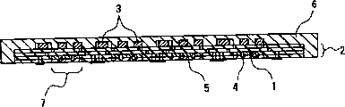
树脂密封后的外形尺寸为,纵向长度为80mm,横向长度80mm,厚度1.6mm,用宽度(L1)5mm的树脂包围基板的整个周围。所得到的成形体的表面透视图示于图7A,其背面透视图示于图7B。此外,其平面图示于图12A,剖视图示于图12B。环氧树脂6将陶瓷多层基板2完全包围,且环氧树脂6其截面形成矩形。The external dimensions after resin sealing were 80 mm in length, 80 mm in width, and 1.6 mm in thickness, and the entire circumference of the substrate was surrounded by resin with a width (L 1 ) of 5 mm. The front perspective view of the obtained molded body is shown in FIG. 7A , and the rear perspective view thereof is shown in FIG. 7B . In addition, its plan view is shown in FIG. 12A, and its cross-sectional view is shown in FIG. 12B. The
在将腔体10制成梯形以便在密封树脂后从金属模中容易取出的情况下,在切割时,由于氧化铝陶瓷基板侧位于上部,在进行处理时,会将应力加在锐角的角部,因此会产生难以被发现的内部裂纹(龟裂)。In the case of making the
但是,如第一及第二种实施形式那样,在陶瓷基板侧的环氧树脂截面形状为矩形时,在处理时不会施加应力,可以防止裂纹。进而,与制成梯形的情况相比,还可以减少树脂密封材料的用量。However, as in the first and second embodiments, when the cross-sectional shape of the epoxy resin on the ceramic substrate side is rectangular, no stress is applied during handling, and cracks can be prevented. Furthermore, compared with the case where it is formed into a trapezoid, it is also possible to reduce the amount of resin sealing material used.
(第三种实施形式)(third implementation form)
下面用图3说明本发明的第三种实施形式。图3是半导体器件树脂密封工艺的简图,8是带有粘接剂的树脂膜,10是上侧金属模的腔体,11是上侧金属模的突起部分,15是金属制框体。该半导体器件与前述第一种实施形式一样,是将半导体元件和外围电路的片状部件安装到陶瓷多层基板上,用传递成形模将陶瓷基板的一个面平坦地进行树脂密封的器件。基板和部件地说明与前述第一种实施形式相同。树脂密封的金属模也和前述第二种实施形式的形式相同。A third embodiment of the present invention will be described below with reference to FIG. 3 . 3 is a schematic diagram of a semiconductor device resin sealing process, 8 is a resin film with an adhesive, 10 is a cavity of an upper metal mold, 11 is a protrusion of an upper metal mold, and 15 is a metal frame. In this semiconductor device, as in the first embodiment, semiconductor elements and peripheral circuit chip components are mounted on a ceramic multilayer substrate, and one surface of the ceramic substrate is flattened and resin-sealed with a transfer molding die. The description of the base plate and components is the same as for the first embodiment described above. The resin-sealed metal mold is also in the same form as the aforementioned second embodiment.
作为制造方法,首先隔开规定的间隙设置基板与金属框体,用带有粘接剂的树脂膜8将两者粘贴。金属框用150mm的方形不锈钢制造,在中央部设置使基板进入的开口部。金属框的宽度30mm,板厚1mm,在中央部具有90mm的方形开口部。树脂膜和第一种实施形式相同。树脂膜的粘贴使用夹具,为了不使树脂起皱,在施加张力的状态下进行粘贴。As a manufacturing method, first, a substrate and a metal frame are provided with a predetermined gap therebetween, and the two are bonded together with an adhesive-attached
其次,将粘贴基板的金属框15固定到下侧金属模上之后,将上下金属模91、92合模。Next, after fixing the
在上侧金属模的腔体部分上,形成包围基板的结构的突起部分11,在金属模合模时,该突起部分11进入金属框体与陶瓷多层基板之间的间隙内。在合模时,前述突起部分11压住树脂膜,控制基板的位置。然后,向腔体10内注入环氧树脂(联苯环氧树脂,日立化成工业社制,商品名“CEL-9200”),进行环氧树脂密封。合模压力,金属模温度,树脂注入压力等成形条件和第二种实施形式相同。On the cavity portion of the upper metal mold, a
在树脂密封时,由于上侧金属模等突起部分直接压紧树脂膜进行基板的位置控制,所以在进行树脂密封时基板不会破裂。此外,第三种实施形式的特征为,由于金属框体15和陶瓷多层基板中间经由树脂片材8成为一个整体,所以,可以简单地向密封金属模上进行装卸。根据这种方法,可以一次同时树脂密封多个基板,大幅度提高操作性能。进而,由于树脂外形稍大于陶瓷基板的大小,树脂的外形比第二种实施形式小,可减少树脂的使用量。也可以提高树脂注入压力。此外,不存在树脂未填充的部位,减少空隙,并且提高在印刷密封方法中比较困难的片状部件与基板间的间隙的填满性,可提高整个成形面的成品率及产品质量。During resin sealing, since the protrusions such as the upper metal mold directly press the resin film to control the position of the substrate, the substrate will not be cracked during resin sealing. Furthermore, the third embodiment is characterized in that since the
树脂密封后的外形尺寸为纵向长度74mm,横向长度74mm,厚度1.6mm,基板的整个周围用宽度(L2)2mm的树脂包围起来。所得成形体的表面的透视图示于图8A,背面透视图示于图8B。此外,图13A为其平面图,图13B为其剖视图。环氧树脂6完全包围陶瓷多层基板2,且环氧树脂6的截面形成矩形。借此,在切割时未发现产生裂纹。The external dimensions after resin sealing were 74 mm in vertical length, 74 mm in lateral length, and 1.6 mm in thickness, and the entire periphery of the substrate was surrounded by resin with a width (L 2 ) of 2 mm. A perspective view of the surface of the obtained molded body is shown in FIG. 8A , and a perspective view of the rear surface is shown in FIG. 8B . In addition, FIG. 13A is a plan view thereof, and FIG. 13B is a cross-sectional view thereof. The
(第四种实施形式)(the fourth implementation form)
下面用图4说明本发明的第四种实施形式。图4是半导体器件的树脂密封工艺的简图,8是带有粘接剂的树脂膜,10是上侧金属模的腔体,11是上侧金属模的突起部分,12是橡胶片材,15是金属框体。该半导体器件和前述第一种实施形式相同、将半导体元件和外围电路的片状部件安装到陶瓷多层基极上,利用传递成形模将陶瓷基板平坦地进行树脂密封。基板与部件的说明与前述第一种实施形式的情况相同。树脂密封金属模的构造也和前述第二种实施形式相同。A fourth embodiment of the present invention will be described below with reference to FIG. 4 . 4 is a schematic diagram of a resin sealing process for a semiconductor device, 8 is a resin film with an adhesive, 10 is a cavity of an upper metal mold, 11 is a protrusion of an upper metal mold, 12 is a rubber sheet, 15 is a metal frame. This semiconductor device is the same as the above-mentioned first embodiment. A semiconductor element and peripheral circuit chip parts are mounted on a ceramic multilayer base, and a ceramic substrate is flatly resin-sealed by a transfer molding die. The description of the substrate and components is the same as that of the aforementioned first embodiment. The structure of the resin-sealed metal mold is also the same as that of the aforementioned second embodiment.
作为制造方法,首先隔开规定的间隙设置基板与金属制框体15,用带有粘接剂的树脂膜8将两者粘贴。金属框15和树脂膜8和第三种实施形式相同。树脂的粘贴用夹具进行,在施加张力的状态下进行粘贴以便树脂膜不会起皱。As a manufacturing method, first, the substrate and the
其次,在密封的下侧金属模的固定基板的部位处,铺设与基板大小一样或大一圈的有机硅树脂等具有橡胶弹性的片材12,将粘贴有基板的金属框固定在其上。橡胶片材12必须具有能够耐受金属模的高温及树脂注入的高压的特征,采用硅酮橡胶片材。硅酮橡胶片材为75mm的方形,其厚度为0.5mm。Next, at the position of fixing the substrate of the lower metal mold of the seal, lay a
在第二种实施形式和第三种实施形式中可以基本上在不破坏基板的情况下对基板进行环氧树脂密封。当由于烧结畸变基板的弯曲较大,超过0.5mm时,或者当弯曲的变化局部地变化很急,像折边一样的情况下,通过如第四种实施形式那样在基板的下面铺设橡胶片材12,可以产生橡胶片吸收、分散和缓和树脂注入时加在基板上的压力的效果,可以不破坏基板地进行密封。In the second and third embodiments, the base plate can be epoxy-sealed substantially without damaging the base plate. When the curvature of the substrate due to sintering distortion is large, exceeding 0.5mm, or when the change of the curvature changes locally rapidly, like a hem, by laying a rubber sheet under the substrate as in the
树脂密封后的外形尺寸为纵向长度74mm,横向长度74mm,厚度1.6mm,基板的整个周围被宽度(L2)2mm的树脂包围。图8A表示其表面透视图,图8B表示其背面透视图。此外,其平面图示于图13A,其剖视图示于图13B。环氧树脂6完全包围陶瓷多层基板2,且环氧树脂6其截面形成矩形。借此,在用切割刀切断时未见到裂纹。The external dimensions after resin sealing were 74 mm in vertical length, 74 mm in lateral length, and 1.6 mm in thickness, and the entire periphery of the substrate was surrounded by resin with a width (L 2 ) of 2 mm. FIG. 8A shows a front perspective view thereof, and FIG. 8B shows a rear perspective view thereof. In addition, its plan view is shown in FIG. 13A, and its cross-sectional view is shown in FIG. 13B. The
(第五种实施形式)(fifth implementation form)
下面利用图5说明本发明的第五种实施形式。图5是半导体器件的树脂密封工艺的简图,11为上侧金属模的突起部分,12为橡胶片材,13为下侧金属模的凹部,15为金属制框体。该半导体器件是前述第四种实施形式的变形形式,使密封的下侧金属模的铺设橡胶片材12的部分凹陷设置阶梯差,凹陷的底部为平坦面,将橡胶片材12放入该凹部内。阶梯差的大小比橡胶片材大一圈,其深度为橡胶片材厚度的一半。橡胶片材为75mm的方形,厚度为0.5mm,阶梯差为77mm的方形,深度0.25mm。这种结构可以限制橡胶片的位置使之不能滑动,并且即使由于基板的弯曲程度不同改变橡胶片材的厚度时,通过调整阶梯差,对于上侧金属模的腔体完全可以不进行任何改变,就可以进行环氧树脂的厚度均匀的密封。A fifth embodiment of the present invention will be described below using FIG. 5 . 5 is a schematic diagram of a resin sealing process of a semiconductor device, 11 is a protrusion of the upper mold, 12 is a rubber sheet, 13 is a concave portion of the lower mold, and 15 is a metal frame. This semiconductor device is a modified form of the aforementioned fourth embodiment. The part of the sealed lower metal mold where the
(第六种实施形式)(the sixth form of implementation)
下面利用图6说明本发明的第六种实施形式。图6是半导体器件的树脂密封工艺的简图,8是带粘接剂的树脂膜,10是上侧金属模的腔体,11是上侧金属模的突起部分,12是橡胶片材,13是下侧金属模的凹部,14是第二树脂膜,15是金属制的框体。该半导体器件是前述第五种实施形式的变形形式,在铺设到密封的下侧金属模上的橡胶片材12与金属框体15的树脂膜8之间夹持第二树脂膜14进行树脂密封。第二树脂膜,其表面是非粘接性的PET(聚对苯二甲酸乙二醇酯),大小为150mm的方形,膜厚25μm。A sixth embodiment of the present invention will be described below using FIG. 6 . 6 is a schematic diagram of a resin sealing process for a semiconductor device, 8 is a resin film with an adhesive, 10 is a cavity of an upper metal mold, 11 is a protrusion of an upper metal mold, 12 is a rubber sheet, 13 A concave portion of the lower mold, 14 is a second resin film, and 15 is a metal frame. This semiconductor device is a modified form of the aforementioned fifth embodiment, and the
用两个金属框夹持固定前述PET膜,以覆盖下侧金属膜的橡胶片材的方式载置固定。金属框为150mm方形的不锈钢制造的,在中央部上设置放入橡胶片材用的开口部。金属框为宽度30mm,厚度0.5mm的双重框,共厚1.0mm,在中央部具有90mm的方形开口。进而,将用树脂膜固定有基板的金属框体载置固定于其上、在把上下金属模91,92合模后进行环氧树脂的密封。The aforementioned PET film was clamped and fixed between two metal frames, and placed and fixed so as to cover the rubber sheet of the lower metal film. The metal frame is made of 150 mm square stainless steel, and an opening for inserting the rubber sheet is provided in the center. The metal frame is a double frame with a width of 30mm and a thickness of 0.5mm, a total thickness of 1.0mm, and a 90mm square opening in the center. Furthermore, the metal frame on which the substrate is fixed with a resin film is placed and fixed thereon, and the upper and
根据前述制造方法,通过在有机硅树脂等橡胶片材上铺设PET膜,可以防止在密封树脂时产生等树脂溢料直接附着在橡胶片材上。由于橡胶片材在其表面上有细的凹凸容易附着灰尘,并且灰尘一旦附着于其上就不能通过吹气将其除去。当在橡胶片材上附着灰尘的状态下原封不动的进行树脂密封时,在基板与橡胶板之间夹杂有硬度不同的异物的情况下施加压力,难免成为新的基板破裂的原因,但由于树脂片材的表面光滑,通过在橡胶片材上铺设树脂片材,可以通过吹气等除去灰尘,可以消除因夹杂灰尘造成基板破裂等可能性。According to the aforementioned manufacturing method, by laying the PET film on the rubber sheet such as silicone resin, it is possible to prevent the resin flash that occurs when the resin is sealed from directly adhering to the rubber sheet. Since the rubber sheet has fine unevenness on its surface, dust tends to adhere, and once the dust adheres thereto, it cannot be removed by air blowing. When resin sealing is performed with dust attached to the rubber sheet, pressure is applied when foreign matter with different hardness is trapped between the substrate and the rubber sheet, which will inevitably cause the new substrate to crack, but due to The surface of the resin sheet is smooth, and by laying the resin sheet on the rubber sheet, dust can be removed by blowing air, etc., and the possibility of cracking the substrate due to dust inclusion can be eliminated.
Claims (6)
Applications Claiming Priority (3)
| Application Number | Priority Date | Filing Date | Title |
|---|---|---|---|
| JP2001382214A JP3560585B2 (en) | 2001-12-14 | 2001-12-14 | Method for manufacturing semiconductor device |
| JP382214/2001 | 2001-12-14 | ||
| JP382214/01 | 2001-12-14 |
Publications (2)
| Publication Number | Publication Date |
|---|---|
| CN1426105A CN1426105A (en) | 2003-06-25 |
| CN1248307C true CN1248307C (en) | 2006-03-29 |
Family
ID=19187426
Family Applications (1)
| Application Number | Title | Priority Date | Filing Date |
|---|---|---|---|
| CNB02132123XA Expired - Lifetime CN1248307C (en) | 2001-12-14 | 2002-08-30 | Semiconductor device and its producing method |
Country Status (5)
| Country | Link |
|---|---|
| US (1) | US6890800B2 (en) |
| JP (1) | JP3560585B2 (en) |
| KR (1) | KR100495644B1 (en) |
| CN (1) | CN1248307C (en) |
| TW (1) | TW554499B (en) |
Families Citing this family (10)
| Publication number | Priority date | Publication date | Assignee | Title |
|---|---|---|---|---|
| JP4094515B2 (en) * | 2003-09-26 | 2008-06-04 | 株式会社ルネサステクノロジ | Manufacturing method of semiconductor device |
| JP4397728B2 (en) * | 2004-04-21 | 2010-01-13 | 日東電工株式会社 | Direct type backlight |
| KR20060102445A (en) * | 2005-03-23 | 2006-09-27 | 박태영 | Set-top box reception chip protection device |
| JP2009004406A (en) * | 2007-06-19 | 2009-01-08 | Disco Abrasive Syst Ltd | Working method for substrate |
| JP5313047B2 (en) * | 2009-05-28 | 2013-10-09 | Towa株式会社 | Mold for resin sealing of electronic parts and resin sealing method |
| JP2015046573A (en) * | 2013-07-31 | 2015-03-12 | 日東電工株式会社 | Attachment jig and method for manufacturing electronic device |
| JP6242763B2 (en) * | 2014-07-18 | 2017-12-06 | Towa株式会社 | Manufacturing method of electronic component package |
| JP7374613B2 (en) * | 2019-05-21 | 2023-11-07 | 日本発條株式会社 | Resin mold circuit body, mold, manufacturing method, and circuit board |
| CN112476713B (en) * | 2019-09-12 | 2022-03-01 | 东莞湧德电子科技有限公司 | Method for manufacturing ceramic heater in electronic cigarette atomizer |
| US11729915B1 (en) | 2022-03-22 | 2023-08-15 | Tactotek Oy | Method for manufacturing a number of electrical nodes, electrical node module, electrical node, and multilayer structure |
Family Cites Families (11)
| Publication number | Priority date | Publication date | Assignee | Title |
|---|---|---|---|---|
| US5200362A (en) | 1989-09-06 | 1993-04-06 | Motorola, Inc. | Method of attaching conductive traces to an encapsulated semiconductor die using a removable transfer film |
| US5851845A (en) * | 1995-12-18 | 1998-12-22 | Micron Technology, Inc. | Process for packaging a semiconductor die using dicing and testing |
| US5776798A (en) | 1996-09-04 | 1998-07-07 | Motorola, Inc. | Semiconductor package and method thereof |
| JPH10135377A (en) | 1996-11-01 | 1998-05-22 | Hitachi Ltd | Mold type semiconductor device |
| JPH11102985A (en) | 1997-09-26 | 1999-04-13 | Mitsubishi Electric Corp | Semiconductor integrated circuit device |
| JP3203228B2 (en) | 1998-03-17 | 2001-08-27 | 三洋電機株式会社 | Semiconductor device and manufacturing method thereof |
| US6326701B1 (en) | 1999-02-24 | 2001-12-04 | Sanyo Electric Co., Ltd. | Chip size package and manufacturing method thereof |
| JP3793679B2 (en) * | 2000-01-31 | 2006-07-05 | Towa株式会社 | Electronic component manufacturing method and manufacturing apparatus |
| JP2001244376A (en) * | 2000-02-28 | 2001-09-07 | Hitachi Ltd | Semiconductor device |
| JP3456462B2 (en) * | 2000-02-28 | 2003-10-14 | 日本電気株式会社 | Semiconductor device and manufacturing method thereof |
| JP2002009097A (en) * | 2000-06-22 | 2002-01-11 | Oki Electric Ind Co Ltd | Semiconductor device and method of manufacturing the same |
-
2001
- 2001-12-14 JP JP2001382214A patent/JP3560585B2/en not_active Expired - Fee Related
-
2002
- 2002-07-29 US US10/208,628 patent/US6890800B2/en not_active Expired - Lifetime
- 2002-07-29 TW TW091116837A patent/TW554499B/en not_active IP Right Cessation
- 2002-08-29 KR KR10-2002-0051409A patent/KR100495644B1/en not_active IP Right Cessation
- 2002-08-30 CN CNB02132123XA patent/CN1248307C/en not_active Expired - Lifetime
Also Published As
| Publication number | Publication date |
|---|---|
| JP3560585B2 (en) | 2004-09-02 |
| KR100495644B1 (en) | 2005-06-14 |
| TW554499B (en) | 2003-09-21 |
| KR20030051175A (en) | 2003-06-25 |
| US6890800B2 (en) | 2005-05-10 |
| CN1426105A (en) | 2003-06-25 |
| JP2003188200A (en) | 2003-07-04 |
| US20030111725A1 (en) | 2003-06-19 |
Similar Documents
| Publication | Publication Date | Title |
|---|---|---|
| CN1211853C (en) | Electronic device, its producing method and its producing device | |
| CN1298034C (en) | Semiconductor package having semiconductor constructing body and method of manufacturing the same | |
| CN1167122C (en) | Semiconductor device | |
| CN1099711C (en) | Semiconductor device and manufacturing method thereof | |
| US7520052B2 (en) | Method of manufacturing a semiconductor device | |
| CN1180471C (en) | Customizable cover for improved thermal performance of modules using the flip-chip method | |
| CN1638071A (en) | Manufacturing method of a semiconductor device | |
| CN1248307C (en) | Semiconductor device and its producing method | |
| CN1925141A (en) | Chip package structure | |
| CN1577841A (en) | Stacked chip semiconductor device and method for manufacturing the same | |
| KR20050114695A (en) | Semiconductor device and method of manufacturing thereof | |
| CN1722931A (en) | Circuit board connection structure and manufacturing method thereof | |
| CN1519920A (en) | Semiconductor device and mfg. method for same | |
| CN1591810A (en) | Mfg. method for emiconductor device | |
| CN1674280A (en) | Stacked electronic part | |
| CN110462854B (en) | Method for manufacturing optoelectronic semiconductor devices | |
| CN1121261A (en) | Lead frames and semiconductor devices | |
| CN1182284A (en) | Lead frame and semiconductor device using same | |
| CN1484072A (en) | Production method of liquid crystal display panel | |
| CN1841688A (en) | Stacked semiconductor device and method for manufacturing stacked electronic component | |
| CN1214452C (en) | Semiconductor device and mfg. method therefor | |
| CN1685501A (en) | Semiconductor device and resin adhesive for assembling semiconductor device | |
| US20210035879A1 (en) | Encapsulated package with carrier, laminate body and component in between | |
| KR20220026496A (en) | Resin molding apparatus and method of manufacturing resin molded product | |
| KR20230034291A (en) | Semiconductor device and its manufacturing method |
Legal Events
| Date | Code | Title | Description |
|---|---|---|---|
| C06 | Publication | ||
| PB01 | Publication | ||
| C10 | Entry into substantive examination | ||
| SE01 | Entry into force of request for substantive examination | ||
| C14 | Grant of patent or utility model | ||
| GR01 | Patent grant | ||
| EE01 | Entry into force of recordation of patent licensing contract |
Assignee: Suzhou Matsushita Semiconductor Co.,Ltd. Assignor: Matsushita Electric Industrial Co.,Ltd. Contract record no.: 2012990000226 Denomination of invention: Method for producing semiconductor device and mask film for said method Granted publication date: 20060329 License type: Common License Open date: 20030625 Record date: 20120413 |
|
| TR01 | Transfer of patent right |
Effective date of registration: 20200527 Address after: Kyoto Japan Patentee after: Panasonic semiconductor solutions Co.,Ltd. Address before: Osaka Japan Patentee before: Matsushita Electric Industrial Co.,Ltd. |
|
| TR01 | Transfer of patent right | ||
| CX01 | Expiry of patent term |
Granted publication date: 20060329 |
|
| CX01 | Expiry of patent term |