CN1195321C - thin film transistor flat panel display - Google Patents
thin film transistor flat panel display Download PDFInfo
- Publication number
- CN1195321C CN1195321C CNB001331884A CN00133188A CN1195321C CN 1195321 C CN1195321 C CN 1195321C CN B001331884 A CNB001331884 A CN B001331884A CN 00133188 A CN00133188 A CN 00133188A CN 1195321 C CN1195321 C CN 1195321C
- Authority
- CN
- China
- Prior art keywords
- layer
- region
- transparent conductive
- gate pad
- gate
- Prior art date
- Legal status (The legal status is an assumption and is not a legal conclusion. Google has not performed a legal analysis and makes no representation as to the accuracy of the status listed.)
- Expired - Lifetime
Links
- 239000010409 thin film Substances 0.000 title claims abstract description 16
- 239000010410 layer Substances 0.000 claims abstract description 264
- 229910052751 metal Inorganic materials 0.000 claims abstract description 61
- 239000002184 metal Substances 0.000 claims abstract description 61
- 239000000758 substrate Substances 0.000 claims abstract description 59
- 229910021417 amorphous silicon Inorganic materials 0.000 claims abstract description 24
- XUIMIQQOPSSXEZ-UHFFFAOYSA-N Silicon Chemical compound [Si] XUIMIQQOPSSXEZ-UHFFFAOYSA-N 0.000 claims abstract description 22
- 229910052710 silicon Inorganic materials 0.000 claims abstract description 22
- 239000010703 silicon Substances 0.000 claims abstract description 22
- 239000011241 protective layer Substances 0.000 claims abstract description 15
- 238000004519 manufacturing process Methods 0.000 claims description 34
- 229920002120 photoresistant polymer Polymers 0.000 claims description 31
- 238000000034 method Methods 0.000 claims description 24
- 238000000151 deposition Methods 0.000 claims description 5
- AMGQUBHHOARCQH-UHFFFAOYSA-N indium;oxotin Chemical compound [In].[Sn]=O AMGQUBHHOARCQH-UHFFFAOYSA-N 0.000 claims description 5
- 238000000059 patterning Methods 0.000 claims description 2
- 239000004065 semiconductor Substances 0.000 description 21
- 238000000206 photolithography Methods 0.000 description 16
- 239000004973 liquid crystal related substance Substances 0.000 description 6
- 239000003990 capacitor Substances 0.000 description 2
- 239000010408 film Substances 0.000 description 2
- 230000001681 protective effect Effects 0.000 description 2
- 238000002834 transmittance Methods 0.000 description 2
- 239000003795 chemical substances by application Substances 0.000 description 1
- 230000000694 effects Effects 0.000 description 1
- 230000005684 electric field Effects 0.000 description 1
- 238000012986 modification Methods 0.000 description 1
- 230000004048 modification Effects 0.000 description 1
- 238000002161 passivation Methods 0.000 description 1
- 230000003068 static effect Effects 0.000 description 1
Images


Landscapes
- Liquid Crystal (AREA)
- Thin Film Transistor (AREA)
Abstract
Description
技术领域technical field
本发明涉及一种薄膜晶体管(thin film transistor,TFT),特别是涉及一种平面显示器的薄膜晶体管。The invention relates to a thin film transistor (thin film transistor, TFT), in particular to a thin film transistor of a flat panel display.
背景技术Background technique
液晶显示器(1iquid crystal display,以下简称LCD)是目前最被广泛使用的一种平面显示器,其具有低消耗电功率、薄型轻量以及低电压驱动等特征,可以应用在个人电脑、文书处理器、导航统、游乐器、投影机、取景器(view finder)以及生活中的手提式机器,例如:手表、电子计算机、电视机等显示使用上。Liquid crystal display (hereinafter referred to as LCD) is the most widely used flat-panel display at present. It has the characteristics of low power consumption, thin and light weight, and low-voltage drive. It can be applied in personal computers, word processors, navigation, etc. Systems, game consoles, projectors, viewfinders, and portable machines in daily life, such as watches, electronic computers, televisions, etc.
LCD的显示原理是利用液晶分子所具有的介电各向异性及导电各向异性,在外加电场时会使液晶分子的排列状态转换,造成液晶薄膜产生各种光电效应。而薄膜晶体管(thin film transistor,以下简称TFT)-LCD即是利用TFT作为主动元件,使其具有低消耗电功率、低电压驱动、薄、轻等优点。但是,TFT的厚度较传统的晶体管薄,使得现有的TFT制作工艺需要多达七道掩模(mask)进行多次光刻制作工艺(photolithography process),因此会产生低产量、高成本等问题。为了有效改善TFT制作工艺的产能与制作成本,目前业界已经提出各种制作方法以及TFT结构,可以尽量减少光刻制作工艺的次数。The display principle of LCD is to use the dielectric anisotropy and conductive anisotropy of liquid crystal molecules. When an electric field is applied, the arrangement state of liquid crystal molecules will be converted, resulting in various photoelectric effects of liquid crystal films. The thin film transistor (thin film transistor, hereinafter referred to as TFT)-LCD uses TFT as an active component, so that it has the advantages of low power consumption, low voltage drive, thin and light. However, the thickness of the TFT is thinner than that of the traditional transistor, so that the existing TFT manufacturing process requires as many as seven masks (mask) for multiple photolithography processes, which will cause problems such as low yield and high cost. In order to effectively improve the production capacity and manufacturing cost of the TFT manufacturing process, various manufacturing methods and TFT structures have been proposed in the industry so far, which can minimize the number of photolithographic manufacturing processes.
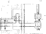
美国专利第5,478,766号中揭示一种TFT-LCD制作工艺,需要使用四次掩模进行光刻制作工艺。请参考图1与图2,图1A至图1C为现有TFT-LCD制作方法所使用的掩模的仰视图,图2A至图2E为现有TFT-LCD制作方法沿图1所示的切线2-2′的剖面示意图。首先,如图1A与图2A所示,将一第一金属层沉积于一基板21上,再利用第一道光刻制作工艺将第一金属层定义形成一栅极电极(gate electrode)22以及一与栅极电极22相连接的栅极线(gate line)。其中,栅极电极22表面上覆盖有一栅极绝缘层23。然后,如图2B所示,依序于基板21上沉积一绝缘层24、一非晶硅(amorphoussilicon,以下简称α-Si)层25以及一掺杂硅层(n+-doped amorphous silicon)26。接着,如图1B与图2C所示,于基板21上沉积一第二金属层之后,利用第二道光刻制作工艺,将第二金属层定义形成一信号线27及一源极/漏极金属层28。后续于基板21上沉积一铟锡氧化物(indiumtin oxide,以下简称ITO)层,并进行第三道光刻制作工艺,将ITO层定义成一信号线区29以及一像素(pixel)区30,如图1C、图2D所示。最后,利用ITO层作为掩模进行第四道光刻制作工艺,将未被ITO层覆盖的源极/漏极金属层28以及掺杂硅层26去除,以定义形成一源极电极31、一漏极电极32以及一接触层23,图2E所示。US Pat. No. 5,478,766 discloses a TFT-LCD manufacturing process, which needs to use four masks for photolithography manufacturing process. Please refer to Fig. 1 and Fig. 2, Fig. 1A to Fig. 1C are the bottom view of the mask used in the existing TFT-LCD manufacturing method, Fig. 2A to Fig. 2E are the tangent line shown in Fig. 1 for the existing TFT-LCD manufacturing method 2-2'Schematic cross-section. First, as shown in FIG. 1A and FIG. 2A, a first metal layer is deposited on a
虽然上述的TFT制作方法已经将光刻制作工艺减低到四次,可以改善TFT制作工艺的产能与制作成本,但是就静电放电(Electrostatic StaticDischarge,以下简称ESD)损害LCD的可靠度的考虑下,现有技术并无法使第一金属层与第二金属层产生电连接,即不能提供用来防止静电放电的防护电路。因此,在减少光刻制作工艺的TFT结构设计下,如何再进一步提供防止ESD的防护电路,便成为当前重要的课题。Although the above-mentioned TFT manufacturing method has reduced the photolithography manufacturing process to four times, which can improve the production capacity and manufacturing cost of the TFT manufacturing process, but considering that Electrostatic Static Discharge (hereinafter referred to as ESD) damages the reliability of LCD, now The prior art cannot electrically connect the first metal layer to the second metal layer, that is, cannot provide a protection circuit for preventing electrostatic discharge. Therefore, how to further provide a protection circuit against ESD under the design of the TFT structure that reduces the photolithography manufacturing process has become an important issue at present.
发明内容Contents of the invention
有鉴于此,本发明的目的在于提出一种薄膜晶体管平面显示器的结构及其制作方法,可以将光刻制作工艺降低至四次,并提供可以防止ESD的防护电路,以解决上述的问题。In view of this, the object of the present invention is to propose a thin film transistor flat panel display structure and its manufacturing method, which can reduce the photolithography manufacturing process to four times, and provide a protection circuit that can prevent ESD, so as to solve the above problems.
根据本发明的一种方案,提供一种薄膜晶体管平面显示器,包括:一基板,其上至少包含一晶体管区及一连接垫区;一栅极电极以及一栅极垫,分别形成于该基板的该晶体管区及该连接垫区中,该栅极垫包含一第一区域及一第二区域;一绝缘层形成于该基板上,以覆盖住该栅极电极以及该栅极垫的第一区域;一非晶硅层,覆盖于该绝缘层上;一掺杂硅层,设于该非晶硅层上;一金属层,设于该掺杂硅层上,用以形成一源极电极以及一漏极电极,该源极电极与该漏极电极间隔一通道;一第一透明导电层,形成于该源极电极、该漏极电极与该基板的表面,但不覆盖该栅极垫;一保护层,形成于该晶体管区及该连接垫区且填满该通道,该保护层覆盖住该源极电极与该漏极电极上的该第一透明导电层以及该栅极垫的第一区域的非晶硅层表面;以及一第二透明导电层,设于未被该保护层所覆盖的区域上,以延伸形成于该栅极垫的第二区域上,且该第二透明导电层与该第一透明导电层连接,使该栅极垫与该金属层产生电连接。According to a solution of the present invention, a thin film transistor flat panel display is provided, comprising: a substrate, which at least includes a transistor region and a connection pad region; a gate electrode and a gate pad, respectively formed on the substrate In the transistor region and the connection pad region, the gate pad includes a first region and a second region; an insulating layer is formed on the substrate to cover the gate electrode and the first region of the gate pad an amorphous silicon layer covering the insulating layer; a doped silicon layer disposed on the amorphous silicon layer; a metal layer disposed on the doped silicon layer for forming a source electrode and a drain electrode, the source electrode is separated from the drain electrode by a channel; a first transparent conductive layer is formed on the surface of the source electrode, the drain electrode and the substrate, but does not cover the gate pad; A protection layer is formed on the transistor region and the connection pad region and fills the channel, the protection layer covers the first transparent conductive layer on the source electrode and the drain electrode and the first layer of the gate pad The surface of the amorphous silicon layer in the area; and a second transparent conductive layer, which is arranged on the area not covered by the protective layer, so as to be extended and formed on the second area of the gate pad, and the second transparent conductive layer It is connected with the first transparent conductive layer, so that the gate pad is electrically connected with the metal layer.
在一实施例中,该基板上还包括一栅极线,而该栅极垫位于该栅极线的末端。该金属层用来形成一垂直于该栅极线的信号线,且该信号线的末端作为一信号垫。In one embodiment, the substrate further includes a gate line, and the gate pad is located at an end of the gate line. The metal layer is used to form a signal line perpendicular to the gate line, and the end of the signal line is used as a signal pad.
在一实施例中,第二透明导电层同时覆盖该栅极垫以及该信号垫,使该栅极线与该信号线产生电连接。在一实施例中,第二透明导电层沿着该栅极垫与该信号垫之间所裸露的该基板表面而覆盖住该栅极垫区的第二区域以及该晶体管区的第一透明导电层,该第一透明导电层覆盖该晶体管区的该金属层表面及该金属层的侧壁上,以使该栅极垫与该晶体管区的该金属层经由第一与第二透明导电层的连接而产生电连接。In one embodiment, the second transparent conductive layer simultaneously covers the gate pad and the signal pad, so that the gate line is electrically connected to the signal line. In one embodiment, the second transparent conductive layer covers the second region of the gate pad region and the first transparent conductive layer of the transistor region along the exposed substrate surface between the gate pad and the signal pad. layer, the first transparent conductive layer covers the surface of the metal layer of the transistor region and the sidewall of the metal layer, so that the gate pad and the metal layer of the transistor region pass through the first and second transparent conductive layers connection to create an electrical connection.
第一与第二透明导电层由铟锡氧化物所构成。掺杂硅层为一N型掺杂硅层。The first and second transparent conductive layers are made of indium tin oxide. The doped silicon layer is an N-type doped silicon layer.
按照本发明的另一方案,提供一种薄膜晶体管平面显示器的制作方法,包括有下列步骤:(a)提供一基板,且该基板上定义有一晶体管区以及一栅极垫区,且该栅极垫区包含有一第一区域以及一第二区域;(b)于该基板表面上沉积一第一金属层,并定义该第一金属层的图案,以分别于该晶体管区与该栅极垫区形成一栅极电极与一栅极垫;(c)依序沉积一绝缘层、一非晶硅层、一掺杂硅层以及一第二金属层,并定义该第二金属层、该掺杂硅层以及该非晶硅层的图案,至少使位于该栅极电极与该栅极垫表面上的该第二金属层、该掺杂硅层以及该非晶硅层形成一岛状结构;(d)于该基板上形成一第一透明导电层,并定义该第一透明导电层的图案,使该第一透明导电层至少覆盖该晶体管区中该第二金属层的部分表面及该基板表面一部分;(e)去除晶体管区中未被该第一透明导电层所覆盖的该第二金属层以及该掺杂硅层,以便将该晶体管区的该第二金属层构图以形成一源极电极以及一漏极电极,该源极电极与漏极电极间隔一通道,并使该通道中的非晶硅层暴露出来;(f)于该晶体管区与该栅极垫区表面上依序形成一保护层以及一具有预定图案的光致抗蚀剂,其中位于该栅极垫区的该光致抗蚀剂只覆盖该第一区域;(g)去除该晶体管区内未被该光致抗蚀剂所覆盖的该保护层,以及该栅极垫区内未被该光致抗蚀剂所覆盖的该保护层、该非晶硅层及该绝缘层;(h)于该基板上形成一第二透明导电层,以覆盖该晶体管区、该栅极垫区、与基板表面的该第一透明导电层;以及(i)进行一浮脱制作工艺,将覆盖于该光致抗蚀剂上的该第二透明导电层以及该光致抗蚀剂去除,而残留的该第二透明导电层可以使该栅极垫与该第二金属层产生电连接。According to another aspect of the present invention, there is provided a method for manufacturing a thin film transistor flat panel display, which includes the following steps: (a) providing a substrate, and defining a transistor region and a gate pad region on the substrate, and the gate The pad area includes a first area and a second area; (b) depositing a first metal layer on the surface of the substrate, and defining the pattern of the first metal layer, so as to separate the transistor area and the gate pad area forming a gate electrode and a gate pad; (c) sequentially depositing an insulating layer, an amorphous silicon layer, a doped silicon layer and a second metal layer, and defining the second metal layer, the doped The silicon layer and the pattern of the amorphous silicon layer at least make the second metal layer, the doped silicon layer and the amorphous silicon layer on the surface of the gate electrode and the gate pad form an island structure; ( d) forming a first transparent conductive layer on the substrate, and defining the pattern of the first transparent conductive layer, so that the first transparent conductive layer covers at least part of the surface of the second metal layer in the transistor region and the surface of the substrate A part; (e) removing the second metal layer and the doped silicon layer not covered by the first transparent conductive layer in the transistor region, so that the second metal layer in the transistor region is patterned to form a source electrode and a drain electrode, the source electrode and the drain electrode are separated by a channel, and the amorphous silicon layer in the channel is exposed; (f) sequentially forming a channel on the surface of the transistor region and the gate pad region protective layer and a photoresist with a predetermined pattern, wherein the photoresist located in the gate pad region only covers the first region; (g) removing the photoresist not covered by the photoresist in the transistor region The protection layer covered by the photoresist, and the protection layer, the amorphous silicon layer and the insulating layer not covered by the photoresist in the gate pad region; (h) forming a first on the substrate Two transparent conductive layers to cover the transistor region, the gate pad region, and the first transparent conductive layer on the surface of the substrate; and (i) performing a lift-off process to cover the photoresist The second transparent conductive layer and the photoresist are removed, and the remaining second transparent conductive layer can make the gate pad and the second metal layer electrically connected.
在一实施例中,步骤(b)中还形成一栅极线,而该栅极垫位于该栅极线的末端。步骤(e)中将该晶体管区的该第二金属层构图,也同时形成一与该栅极线垂直的信号线,且该信号线的末端作为一信号垫。步骤(g)中将该光致抗蚀剂覆盖住该栅极垫区的部分表面,使得该栅极垫与该信号垫之间的基板表面裸露出来,并使该裸露的基板附近的栅极垫的一部分表面裸露出来。In one embodiment, a gate line is further formed in step (b), and the gate pad is located at the end of the gate line. In step (e), patterning the second metal layer in the transistor region also forms a signal line perpendicular to the gate line at the same time, and the end of the signal line serves as a signal pad. In step (g), the photoresist covers part of the surface of the gate pad region, so that the substrate surface between the gate pad and the signal pad is exposed, and the gate near the exposed substrate is exposed. Part of the surface of the pad is exposed.
在一实施例中,步骤(i)使该第二透明导电层同时覆盖该栅极垫以及该信号垫,使该栅极线与该信号线产生电连接。在一实施例中,步骤(i)使该第二透明导电层沿着该栅极垫与该信号垫之间所裸露的该基板表面而覆盖住该栅极垫的第二区域及该晶体管区的该第一透明导电层,使得该栅极垫与该晶体管区的该第二金属层经由第一与第二透明导电层的连接而产生电连接。In one embodiment, step (i) makes the second transparent conductive layer cover the gate pad and the signal pad at the same time, so that the gate line and the signal line are electrically connected. In one embodiment, step (i) makes the second transparent conductive layer cover the second region of the gate pad and the transistor region along the exposed surface of the substrate between the gate pad and the signal pad The first transparent conductive layer, so that the gate pad and the second metal layer of the transistor region are electrically connected through the connection between the first and second transparent conductive layers.
在一实施例中,保护层填满该通道。In one embodiment, a protective layer fills the channel.
本发明的晶体管结构的制作上只需利用四道光刻制作工艺,因此可以有效提高其产能,并降低制作成本。而且,本发明于制作液晶显示器时,利用具有预定图案的光致抗蚀剂来进行第四光刻制作工艺,去除连接垫区中部分的保护层、非晶硅层、以及绝缘层,使第二透明导电层可形成于栅极垫的裸露的表面上。之后,利用浮脱(lift-off)制作工艺,将光致抗蚀剂上的第二透明导电层与光致抗蚀剂一起移除,如此可去除不需要的第二透明导电层。此外第二透明导电层覆盖部分的第一透明导电层,而第一透明导电层亦覆盖晶体管区的源极/漏极电极,经由第一透明导电层与第二透明导电层的连接,可以达到栅极垫与形成源极/漏极电极的第二金属层相连接的目的。此外,栅极垫区附近的基板表面上的绝缘层也会被去除,使第二透明导电层直接形成于基板的裸露的表面上,因此这个像素区的透光率会明显增加许多,对于提升液晶显示器的显示品质有很大的帮助。第一透明导电层或第二透明导电层构成像素区域中的像素电极。第一透明导电层或第二透明导电层亦可以形成于栅极线末端的栅极垫与信号线末端的信号垫之间,如此同样达到栅极垫与形成信号线的第二金属层相连接的目的,以形成防止静电放电的保护电路。The manufacturing of the transistor structure of the present invention only needs to use four photolithography manufacturing processes, so the production capacity can be effectively improved and the manufacturing cost can be reduced. Moreover, when the present invention is making a liquid crystal display, a photoresist with a predetermined pattern is used to carry out the fourth photolithography manufacturing process, and the protective layer, the amorphous silicon layer, and the insulating layer in the connection pad area are removed, so that the first Two transparent conductive layers can be formed on the exposed surfaces of the gate pads. Afterwards, the second transparent conductive layer on the photoresist is removed together with the photoresist by using a lift-off process, so that the unnecessary second transparent conductive layer can be removed. In addition, the second transparent conductive layer covers part of the first transparent conductive layer, and the first transparent conductive layer also covers the source/drain electrodes of the transistor region. Through the connection between the first transparent conductive layer and the second transparent conductive layer, it can achieve The purpose of the gate pad being connected to the second metal layer forming the source/drain electrodes. In addition, the insulating layer on the substrate surface near the gate pad region will also be removed, so that the second transparent conductive layer is directly formed on the exposed surface of the substrate, so the light transmittance of this pixel region will increase significantly, which is very important for improving The display quality of the LCD helps a lot. The first transparent conductive layer or the second transparent conductive layer constitutes a pixel electrode in the pixel area. The first transparent conductive layer or the second transparent conductive layer can also be formed between the gate pad at the end of the gate line and the signal pad at the end of the signal line, so that the gate pad is also connected to the second metal layer forming the signal line purpose to form a protective circuit against electrostatic discharge.
附图说明Description of drawings
为使本发明的上述目的、特征、和优点能更明显易懂,下文特举一优选实施例,并配合附图作详细说明。附图中:In order to make the above-mentioned objects, features, and advantages of the present invention more comprehensible, a preferred embodiment is specifically cited below and described in detail with accompanying drawings. In the attached picture:
图1A~1C显示现有薄膜晶体管平面显示器制作方法流程的仰视图。1A-1C show the bottom view of the manufacturing process of the conventional thin film transistor flat panel display.
图2A~2E为沿图1的切线2-2′的剖面示意图。2A-2E are schematic cross-sectional views along the line 2-2' of FIG. 1 .
图3A~3E显示本发明薄膜晶体管平面显示器制作方法流程的仰视图。3A to 3E are bottom views showing the process flow of the manufacturing method of the thin film transistor flat panel display of the present invention.
图4A~4E为沿图3的切线I-I′、II-II′、III-III′的剖面示意图。4A-4E are schematic cross-sectional views along the tangent lines I-I', II-II', and III-III' in FIG. 3 .
图5为沿图3E切线5-5′的剖面示意图。FIG. 5 is a schematic cross-sectional view along line 5-5' in FIG. 3E.
附图的符号说明:Explanation of the symbols of the accompanying drawings:
基板~41;第一金属层~40;栅极电极~42;栅极线~43;栅极垫~44;栅极绝缘层~46;第一半导体层~48;第二半导体层~50;第二金属层~52;第一透明导电层~54;信号线~55;源极电极~561;漏极电极~562;信号垫~57;通道~59;保护层~58;光致抗蚀剂~60;第二透明导电层~62。Substrate ~ 41; first metal layer ~ 40; gate electrode ~ 42; gate line ~ 43; gate pad ~ 44; gate insulating layer ~ 46; first semiconductor layer ~ 48; second semiconductor layer ~ 50; Second metal layer ~ 52; first transparent conductive layer ~ 54; signal line ~ 55; source electrode ~ 561; drain electrode ~ 562; signal pad ~ 57; channel ~ 59; protective layer ~ 58; photoresist Agent ~ 60; second transparent conductive layer ~ 62.
具体实施方式Detailed ways
以下将配合附图详细说明本发明的优选实施例。Preferred embodiments of the present invention will be described in detail below with reference to the accompanying drawings.
请参考图3与图4,图3A至图3E为本发明薄膜晶体管平面显示器制作方法的仰视图,图4A至图4E为沿图3的切线I-I′、II-II′、III-III′的剖面示意图,其中图4的I区域为沿切线I-I′的剖面示意图、II区域为沿切线II-II′的剖面示意图、III区域为沿切线III-III′的剖面示意图。首先,提供一基板41,其上设有一晶体管区(以下称TFT区,I区域)、一电容区(II区域)以及一栅极垫区(III区域)。然后,如图3A与图4A所示,将一第一金属层沉积于基板41上,再利用一第一光刻制作工艺将第一金属层定义形成一栅极电极42、一栅极线43以及一栅极垫44。其中栅极电极42位于TFT区,栅极线43与栅极电极42连接,而栅极垫44位于栅极线43的末端。Please refer to FIG. 3 and FIG. 4. FIG. 3A to FIG. 3E are bottom views of the manufacturing method of the thin film transistor flat panel display of the present invention, and FIG. 4A to FIG. Schematic cross-sectional view, wherein the I area of Fig. 4 is a schematic cross-sectional view along the tangent line II', the II area is a schematic cross-sectional view along the tangent line II-II', and the III area is a schematic cross-sectional view along the tangent line III-III'. First, a
然后,如图3B与图4B所示,依序于基板41上沉积一栅极绝缘层46、一第一半导体层48、一第二半导体层50以及一第二金属层52。接着,进行一第二光刻制作工艺,去除一预定区域外的第二金属层52、第二半导体层50以及第一半导体层48,最后分别于TFT区以及栅极垫区定义形成一岛状(island)结构。其中,第一半导体层48为非晶硅层,第二半导体层50为掺杂硅层。Then, as shown in FIG. 3B and FIG. 4B , a
接着,如图3C与图4C所示,于基板41表面的预定像素(pixel)区域上形成一第一透明导电层54,用来作为一像素电极,再进行一第三光刻制作工艺,去除未被第一透明导电层54所覆盖的第二金属层52以及第二半导体层50,以便形成一信号线(signal line)55以及一源极/漏极电极561、562。其中,源极/漏极电极561、562之间具有一通道59,贯穿第一透明导电层54、第二金属层52与第二半导体层50。信号线55垂直于栅极线43,且信号线55的末端作为一信号垫(signal pad)57。此外,栅极垫区的第二金属层52以及第二半导体层50会被完全去除,以使栅极垫区的第一半导体层48表面暴露出来。Next, as shown in FIG. 3C and FIG. 4C, a first transparent
其后,如图3D与图4D所示,于基板41表面上沉积一保护层58,该保护层填满通道59。再于保护层58表面上形成一具有预定图案的光致抗蚀剂60,使其覆盖TFT区及一部分的栅极垫区表面。该栅极垫区III分为A区域及B区域,位于栅极垫区III中的光致抗蚀剂60只覆盖B区域。随后进行一第四光刻制作工艺,去除A区域中未被光致抗蚀剂60所覆盖的保护层58、第一半导体层48与绝缘层46。如此一来,不但使栅极垫区III的A区域中的基板41表面裸露出来,还使信号垫57与栅极垫44之间的基板41表面裸露出来(未图示)。然后,于基板41表面上形成一第二透明导电层62,使其覆盖晶体管区I的光致抗蚀剂60、电容区II的第一透明导电层54、栅极垫区III中A区域、以及栅极垫区III中B区域的光致抗蚀剂层60。Thereafter, as shown in FIG. 3D and FIG. 4D , a
最后,如图3E与图4E所示,进行一浮脱(lift-off)制作工艺,将覆盖于光致抗蚀剂60上的第二透明导电层62以及光致抗蚀剂60完全去除。如此一来,晶体管区I中残留的第二透明导电层62覆盖保护层58的侧壁部分以及第一透明导电层54裸露的表面。而且在栅极垫区III中残留的第二透明导电层62只覆盖住栅极垫区III的A区域的栅极垫44与基板41的裸露表面,并且不覆盖栅极垫区III的B区域。Finally, as shown in FIG. 3E and FIG. 4E , a lift-off process is performed to completely remove the second transparent
请参考图5,图5为沿图3E切线5-5′的剖面示意图。进行完成浮脱制作工艺之后,第二透明导电层62会覆盖住栅极垫44的裸露表面,并沿着信号垫57(未图示)与栅极垫44之间的基板41表面延伸,最后接触第一透明导电层54,而且保护层58会覆盖第二金属层52的侧壁。如此一来,第二透明导电层62便能够使栅极垫44与第二金属层52产生电连接,以便形成可以防止静电放电的防护电路。Please refer to FIG. 5 , which is a schematic cross-sectional view along line 5 - 5 ′ in FIG. 3E . After the lift-off manufacturing process is completed, the second transparent
依据上述的制作方法,本发明揭露一种薄膜晶体管平面显示器,该显示器包括有一基板,基板上至少包含一晶体管区及一连接垫区。一栅极电极(gate electrode)以及一栅极垫(gate pad)分别形成于基板上的晶体管区及连接垫区中,栅极垫包含一第一区域及一第二区域。一绝缘层还形成于基板上,以覆盖住栅极电极以及栅极垫的第一区域。一第一半导体层覆盖于绝缘层上,一第二半导体层设于该第一半导体薄膜的一预定区域上,一金属层设于该第二半导体层上,用以形成一源极(source)电极以及一漏极(drain)电极,该源极电极与该漏极电极间隔一通道(channel)。此外,一第一透明导电层形成于源极电极、漏极电极、与基板的表面,但不覆盖栅极垫。一保护层形成于晶体管区及连接垫区且填满该晶体管区的通道,保护层覆盖住源极电极与漏极电极上的第一透明导电层以及栅极垫上的第一半导体层表面的第一区域。最后,一第二透明导电层设于未被保护层所覆盖的区域上,以延伸形成于栅极垫的第二区域上,且第二透明导电层与第一透明导电层连接,使栅极垫与金属层产生电连接。According to the above manufacturing method, the present invention discloses a thin film transistor flat panel display, which includes a substrate, and the substrate at least includes a transistor region and a connection pad region. A gate electrode and a gate pad are respectively formed in the transistor region and the connection pad region on the substrate, and the gate pad includes a first region and a second region. An insulating layer is also formed on the substrate to cover the gate electrode and the first area of the gate pad. A first semiconductor layer covers the insulating layer, a second semiconductor layer is arranged on a predetermined region of the first semiconductor film, and a metal layer is arranged on the second semiconductor layer to form a source (source) electrode and a drain electrode, the source electrode is separated from the drain electrode by a channel. In addition, a first transparent conductive layer is formed on the surface of the source electrode, the drain electrode, and the substrate, but does not cover the gate pad. A protection layer is formed on the transistor region and the connection pad region and fills the channel of the transistor region. The protection layer covers the first transparent conductive layer on the source electrode and the drain electrode and the first semiconductor layer on the gate pad. an area. Finally, a second transparent conductive layer is provided on the area not covered by the protection layer to extend and form on the second area of the grid pad, and the second transparent conductive layer is connected with the first transparent conductive layer to make the grid The pad makes electrical connection with the metal layer.
第一半导体层为一非晶硅(amorphous silicon)层,第二半导体层为一掺杂硅层,第一、第二透明导电层均由铟锡氧化物(indium tin oxide,ITO)所构成。The first semiconductor layer is an amorphous silicon layer, the second semiconductor layer is a doped silicon layer, and the first and second transparent conductive layers are both made of indium tin oxide (ITO).
本发明的晶体管结构的制作上只需利用四道光刻制作工艺,因此可以有效提高其产能,并降低制作成本。而且,本发明于制作液晶显示器时,利用具有预定图案的光致抗蚀剂来进行第四光刻制作工艺,去除连接垫区中部分的保护层、第一半导体层、以及绝缘层,使第二透明导电层可形成于栅极垫的裸露的表面上。之后,利用浮脱(lift-off)制作工艺,将光致抗蚀剂上的第二透明导电层与光致抗蚀剂一起移除,如此可去除不需要的第二透明导电层。此外第二透明导电层覆盖部分的第一透明导电层,而第一透明导电层亦覆盖晶体管区的源极/漏极电极,经由第一透明导电层与第二透明导电层的连接,可以达到栅极垫与形成源极/漏极电极的第二金属层相连接的目的。此外,栅极垫区附近的基板表面上的绝缘层也会被去除,使第二透明导电层直接形成于基板的裸露的表面上,因此这个像素区的透光率会明显增加许多,对于提升液晶显示器的显示品质有很大的帮助。第一透明导电层或第二透明导电层构成像素区域中的像素电极。第一透明导电层或第二透明导电层亦可以形成于栅极线末端的栅极垫与信号线末端的信号垫之间,如此同样达到栅极垫与形成信号线的第二金属层相连接的目的,以形成防止静电放电的保护电路。The manufacturing of the transistor structure of the present invention only needs to use four photolithography manufacturing processes, so the production capacity can be effectively improved and the manufacturing cost can be reduced. Moreover, when the present invention is making a liquid crystal display, a photoresist with a predetermined pattern is used to carry out a fourth photolithography process to remove the protective layer, the first semiconductor layer, and the insulating layer in the connection pad region, so that the second Two transparent conductive layers can be formed on the exposed surfaces of the gate pads. Afterwards, the second transparent conductive layer on the photoresist is removed together with the photoresist by using a lift-off process, so that the unnecessary second transparent conductive layer can be removed. In addition, the second transparent conductive layer covers part of the first transparent conductive layer, and the first transparent conductive layer also covers the source/drain electrodes of the transistor region. Through the connection between the first transparent conductive layer and the second transparent conductive layer, it can achieve The purpose of the gate pad being connected to the second metal layer forming the source/drain electrodes. In addition, the insulating layer on the substrate surface near the gate pad region will also be removed, so that the second transparent conductive layer is directly formed on the exposed surface of the substrate, so the light transmittance of this pixel region will be significantly increased, which is very important for improving The display quality of the LCD helps a lot. The first transparent conductive layer or the second transparent conductive layer constitutes a pixel electrode in the pixel area. The first transparent conductive layer or the second transparent conductive layer can also be formed between the gate pad at the end of the gate line and the signal pad at the end of the signal line, so that the gate pad is also connected to the second metal layer forming the signal line purpose to form a protective circuit against electrostatic discharge.
虽然本发明已结合一优选实施例揭露如上,然而其并非用以限定本发明,本领域的技术人员在不脱离本发明的精神和范围内,应当可以作出各种更动与润饰,因此本发明的保护范围应当以权利要求的界定为准。Although the present invention has been disclosed above in conjunction with a preferred embodiment, it is not intended to limit the present invention. Those skilled in the art should be able to make various changes and modifications without departing from the spirit and scope of the present invention. Therefore, the present invention The scope of protection should be defined by the claims.
Claims (14)
Priority Applications (1)
| Application Number | Priority Date | Filing Date | Title |
|---|---|---|---|
| CNB001331884A CN1195321C (en) | 2000-10-24 | 2000-10-24 | thin film transistor flat panel display |
Applications Claiming Priority (1)
| Application Number | Priority Date | Filing Date | Title |
|---|---|---|---|
| CNB001331884A CN1195321C (en) | 2000-10-24 | 2000-10-24 | thin film transistor flat panel display |
Publications (2)
| Publication Number | Publication Date |
|---|---|
| CN1350326A CN1350326A (en) | 2002-05-22 |
| CN1195321C true CN1195321C (en) | 2005-03-30 |
Family
ID=4595545
Family Applications (1)
| Application Number | Title | Priority Date | Filing Date |
|---|---|---|---|
| CNB001331884A Expired - Lifetime CN1195321C (en) | 2000-10-24 | 2000-10-24 | thin film transistor flat panel display |
Country Status (1)
| Country | Link |
|---|---|
| CN (1) | CN1195321C (en) |
Families Citing this family (21)
| Publication number | Priority date | Publication date | Assignee | Title |
|---|---|---|---|---|
| CN1333432C (en) * | 2003-08-21 | 2007-08-22 | 广辉电子股份有限公司 | Manufacturing method of thin film transistor array substrate |
| KR100982122B1 (en) * | 2003-12-30 | 2010-09-14 | 엘지디스플레이 주식회사 | Poor pixel darkening method of horizontal field applied thin film transistor substrate |
| CN100397213C (en) * | 2003-12-31 | 2008-06-25 | 友达光电股份有限公司 | Method for manufacturing thin film transistor array substrate |
| CN1308749C (en) * | 2004-09-28 | 2007-04-04 | 友达光电股份有限公司 | Manufacturing method of flat display panel |
| KR100645718B1 (en) | 2005-04-28 | 2006-11-14 | 삼성에스디아이 주식회사 | Thin Film Transistor and Manufacturing Method Thereof |
| CN100576045C (en) * | 2007-08-31 | 2009-12-30 | 友达光电股份有限公司 | Liquid crystal display device and method for manufacturing the same |
| US12496809B2 (en) | 2010-11-08 | 2025-12-16 | View Operating Corporation | Electrochromic window fabrication methods |
| US9958750B2 (en) | 2010-11-08 | 2018-05-01 | View, Inc. | Electrochromic window fabrication methods |
| CN113359364A (en) | 2011-12-12 | 2021-09-07 | 唯景公司 | Thin film devices and fabrication |
| US10295880B2 (en) | 2011-12-12 | 2019-05-21 | View, Inc. | Narrow pre-deposition laser deletion |
| WO2016004373A1 (en) * | 2014-07-03 | 2016-01-07 | View, Inc. | Narrow pre-deposition laser deletion |
| US10802371B2 (en) | 2011-12-12 | 2020-10-13 | View, Inc. | Thin-film devices and fabrication |
| US11865632B2 (en) | 2011-12-12 | 2024-01-09 | View, Inc. | Thin-film devices and fabrication |
| US12061402B2 (en) | 2011-12-12 | 2024-08-13 | View, Inc. | Narrow pre-deposition laser deletion |
| US12403676B2 (en) | 2011-12-12 | 2025-09-02 | View Operating Corporation | Thin-film devices and fabrication |
| CN103984171A (en) * | 2013-02-22 | 2014-08-13 | 上海天马微电子有限公司 | Array substrate, manufacturing method thereof and liquid crystal display |
| US12235560B2 (en) | 2014-11-25 | 2025-02-25 | View, Inc. | Faster switching electrochromic devices |
| CA2980477A1 (en) | 2015-03-20 | 2016-09-29 | View, Inc. | Faster switching low-defect electrochromic windows |
| CN105093762B (en) | 2015-09-28 | 2019-01-11 | 京东方科技集团股份有限公司 | array substrate, manufacturing method and corresponding display panel and electronic device |
| CN112817173B (en) * | 2021-01-05 | 2023-10-17 | 深圳市华星光电半导体显示技术有限公司 | Sensing assembly, manufacturing method thereof and display panel |
| CN116364780B (en) * | 2023-03-27 | 2024-10-01 | 惠科股份有限公司 | Thin film transistor and manufacturing method thereof, electrostatic discharge protection circuit and display device |
-
2000
- 2000-10-24 CN CNB001331884A patent/CN1195321C/en not_active Expired - Lifetime
Also Published As
| Publication number | Publication date |
|---|---|
| CN1350326A (en) | 2002-05-22 |
Similar Documents
| Publication | Publication Date | Title |
|---|---|---|
| CN1195321C (en) | thin film transistor flat panel display | |
| TWI440945B (en) | Array substrate for edge field switching mode liquid crystal display device and method of fabricating the same | |
| CN1170196C (en) | Method for manufacturing thin film transistor liquid crystal display | |
| CN102033379B (en) | Liquid crystal display and manufacturing method thereof | |
| JP5950638B2 (en) | Wiring structure, thin film transistor array substrate including the same, and display device | |
| KR20050067934A (en) | Method for forming metal line and method for manufacturing liquid crystal display device using the same | |
| CN1151406C (en) | Thin film transistor liquid crystal display and method of fabricating the same | |
| KR20020058270A (en) | array panel of liquid crystal display and manufacturing method thereof | |
| TWI253538B (en) | Thin film transistor flat display and its manufacturing method | |
| CN103280428B (en) | TFT-LCD arraying bread board structure and manufacture method thereof | |
| CN1185534C (en) | Active matrix substrate of liquid crystal display device and manufacturing method thereof | |
| CN108538859A (en) | The production method of array substrate | |
| US6440783B2 (en) | Method for fabricating a thin film transistor display | |
| US7335538B2 (en) | Method for manufacturing bottom substrate of liquid crystal display device | |
| CN1892373A (en) | Thin film transistor substrate and fabricating method thereof | |
| CN101150093B (en) | Method for manufacturing pixel structure | |
| KR100493380B1 (en) | Method for manufacturing liquid crystal display device | |
| CN1187643C (en) | Active matrix substrate of liquid crystal display device and manufacturing method thereof | |
| KR101294689B1 (en) | Method of Fabricating Fringe Field Switching Mode Liquid Crystal Display Device | |
| TWM628882U (en) | Improved structure of lcd panel | |
| KR100190035B1 (en) | Manufacturing method of liquid crystal display device | |
| KR100646172B1 (en) | LCD and its manufacturing method | |
| KR100583313B1 (en) | LCD and its manufacturing method | |
| JPH02272774A (en) | Active matrix circuit board | |
| CN2618187Y (en) | Thin Film Transistor Liquid Crystal Display |
Legal Events
| Date | Code | Title | Description |
|---|---|---|---|
| C10 | Entry into substantive examination | ||
| SE01 | Entry into force of request for substantive examination | ||
| C06 | Publication | ||
| PB01 | Publication | ||
| C14 | Grant of patent or utility model | ||
| GR01 | Patent grant | ||
| CX01 | Expiry of patent term | ||
| CX01 | Expiry of patent term |
Granted publication date: 20050330 |