CN116250060A - A surface connector of a semiconductor chip and its preparation method and application - Google Patents
A surface connector of a semiconductor chip and its preparation method and application Download PDFInfo
- Publication number
- CN116250060A CN116250060A CN202180060371.7A CN202180060371A CN116250060A CN 116250060 A CN116250060 A CN 116250060A CN 202180060371 A CN202180060371 A CN 202180060371A CN 116250060 A CN116250060 A CN 116250060A
- Authority
- CN
- China
- Prior art keywords
- chip
- molecules
- chip surface
- preparation
- molecule
- Prior art date
- Legal status (The legal status is an assumption and is not a legal conclusion. Google has not performed a legal analysis and makes no representation as to the accuracy of the status listed.)
- Pending
Links
Images


Classifications
-
- C—CHEMISTRY; METALLURGY
- C12—BIOCHEMISTRY; BEER; SPIRITS; WINE; VINEGAR; MICROBIOLOGY; ENZYMOLOGY; MUTATION OR GENETIC ENGINEERING
- C12Q—MEASURING OR TESTING PROCESSES INVOLVING ENZYMES, NUCLEIC ACIDS OR MICROORGANISMS; COMPOSITIONS OR TEST PAPERS THEREFOR; PROCESSES OF PREPARING SUCH COMPOSITIONS; CONDITION-RESPONSIVE CONTROL IN MICROBIOLOGICAL OR ENZYMOLOGICAL PROCESSES
- C12Q1/00—Measuring or testing processes involving enzymes, nucleic acids or microorganisms; Compositions therefor; Processes of preparing such compositions
- C12Q1/68—Measuring or testing processes involving enzymes, nucleic acids or microorganisms; Compositions therefor; Processes of preparing such compositions involving nucleic acids
- C12Q1/6813—Hybridisation assays
- C12Q1/6834—Enzymatic or biochemical coupling of nucleic acids to a solid phase
- C12Q1/6837—Enzymatic or biochemical coupling of nucleic acids to a solid phase using probe arrays or probe chips
-
- B—PERFORMING OPERATIONS; TRANSPORTING
- B01—PHYSICAL OR CHEMICAL PROCESSES OR APPARATUS IN GENERAL
- B01J—CHEMICAL OR PHYSICAL PROCESSES, e.g. CATALYSIS OR COLLOID CHEMISTRY; THEIR RELEVANT APPARATUS
- B01J19/00—Chemical, physical or physico-chemical processes in general; Their relevant apparatus
- B01J19/0046—Sequential or parallel reactions, e.g. for the synthesis of polypeptides or polynucleotides; Apparatus and devices for combinatorial chemistry or for making molecular arrays
-
- C—CHEMISTRY; METALLURGY
- C12—BIOCHEMISTRY; BEER; SPIRITS; WINE; VINEGAR; MICROBIOLOGY; ENZYMOLOGY; MUTATION OR GENETIC ENGINEERING
- C12Q—MEASURING OR TESTING PROCESSES INVOLVING ENZYMES, NUCLEIC ACIDS OR MICROORGANISMS; COMPOSITIONS OR TEST PAPERS THEREFOR; PROCESSES OF PREPARING SUCH COMPOSITIONS; CONDITION-RESPONSIVE CONTROL IN MICROBIOLOGICAL OR ENZYMOLOGICAL PROCESSES
- C12Q1/00—Measuring or testing processes involving enzymes, nucleic acids or microorganisms; Compositions therefor; Processes of preparing such compositions
- C12Q1/68—Measuring or testing processes involving enzymes, nucleic acids or microorganisms; Compositions therefor; Processes of preparing such compositions involving nucleic acids
-
- B—PERFORMING OPERATIONS; TRANSPORTING
- B01—PHYSICAL OR CHEMICAL PROCESSES OR APPARATUS IN GENERAL
- B01J—CHEMICAL OR PHYSICAL PROCESSES, e.g. CATALYSIS OR COLLOID CHEMISTRY; THEIR RELEVANT APPARATUS
- B01J2219/00—Chemical, physical or physico-chemical processes in general; Their relevant apparatus
- B01J2219/00274—Sequential or parallel reactions; Apparatus and devices for combinatorial chemistry or for making arrays; Chemical library technology
- B01J2219/00277—Apparatus
- B01J2219/0054—Means for coding or tagging the apparatus or the reagents
- B01J2219/00572—Chemical means
- B01J2219/00576—Chemical means fluorophore
-
- B—PERFORMING OPERATIONS; TRANSPORTING
- B01—PHYSICAL OR CHEMICAL PROCESSES OR APPARATUS IN GENERAL
- B01J—CHEMICAL OR PHYSICAL PROCESSES, e.g. CATALYSIS OR COLLOID CHEMISTRY; THEIR RELEVANT APPARATUS
- B01J2219/00—Chemical, physical or physico-chemical processes in general; Their relevant apparatus
- B01J2219/00274—Sequential or parallel reactions; Apparatus and devices for combinatorial chemistry or for making arrays; Chemical library technology
- B01J2219/00583—Features relative to the processes being carried out
- B01J2219/00603—Making arrays on substantially continuous surfaces
- B01J2219/00605—Making arrays on substantially continuous surfaces the compounds being directly bound or immobilised to solid supports
- B01J2219/00608—DNA chips
-
- B—PERFORMING OPERATIONS; TRANSPORTING
- B01—PHYSICAL OR CHEMICAL PROCESSES OR APPARATUS IN GENERAL
- B01J—CHEMICAL OR PHYSICAL PROCESSES, e.g. CATALYSIS OR COLLOID CHEMISTRY; THEIR RELEVANT APPARATUS
- B01J2219/00—Chemical, physical or physico-chemical processes in general; Their relevant apparatus
- B01J2219/00274—Sequential or parallel reactions; Apparatus and devices for combinatorial chemistry or for making arrays; Chemical library technology
- B01J2219/00583—Features relative to the processes being carried out
- B01J2219/00603—Making arrays on substantially continuous surfaces
- B01J2219/00605—Making arrays on substantially continuous surfaces the compounds being directly bound or immobilised to solid supports
- B01J2219/00612—Making arrays on substantially continuous surfaces the compounds being directly bound or immobilised to solid supports the surface being inorganic
-
- B—PERFORMING OPERATIONS; TRANSPORTING
- B01—PHYSICAL OR CHEMICAL PROCESSES OR APPARATUS IN GENERAL
- B01J—CHEMICAL OR PHYSICAL PROCESSES, e.g. CATALYSIS OR COLLOID CHEMISTRY; THEIR RELEVANT APPARATUS
- B01J2219/00—Chemical, physical or physico-chemical processes in general; Their relevant apparatus
- B01J2219/00274—Sequential or parallel reactions; Apparatus and devices for combinatorial chemistry or for making arrays; Chemical library technology
- B01J2219/00583—Features relative to the processes being carried out
- B01J2219/00603—Making arrays on substantially continuous surfaces
- B01J2219/00605—Making arrays on substantially continuous surfaces the compounds being directly bound or immobilised to solid supports
- B01J2219/00623—Immobilisation or binding
- B01J2219/00626—Covalent
-
- B—PERFORMING OPERATIONS; TRANSPORTING
- B01—PHYSICAL OR CHEMICAL PROCESSES OR APPARATUS IN GENERAL
- B01J—CHEMICAL OR PHYSICAL PROCESSES, e.g. CATALYSIS OR COLLOID CHEMISTRY; THEIR RELEVANT APPARATUS
- B01J2219/00—Chemical, physical or physico-chemical processes in general; Their relevant apparatus
- B01J2219/00274—Sequential or parallel reactions; Apparatus and devices for combinatorial chemistry or for making arrays; Chemical library technology
- B01J2219/00583—Features relative to the processes being carried out
- B01J2219/00603—Making arrays on substantially continuous surfaces
- B01J2219/00605—Making arrays on substantially continuous surfaces the compounds being directly bound or immobilised to solid supports
- B01J2219/00632—Introduction of reactive groups to the surface
-
- B—PERFORMING OPERATIONS; TRANSPORTING
- B01—PHYSICAL OR CHEMICAL PROCESSES OR APPARATUS IN GENERAL
- B01J—CHEMICAL OR PHYSICAL PROCESSES, e.g. CATALYSIS OR COLLOID CHEMISTRY; THEIR RELEVANT APPARATUS
- B01J2219/00—Chemical, physical or physico-chemical processes in general; Their relevant apparatus
- B01J2219/00274—Sequential or parallel reactions; Apparatus and devices for combinatorial chemistry or for making arrays; Chemical library technology
- B01J2219/00718—Type of compounds synthesised
- B01J2219/0072—Organic compounds
- B01J2219/00722—Nucleotides
Landscapes
- Chemical & Material Sciences (AREA)
- Organic Chemistry (AREA)
- Life Sciences & Earth Sciences (AREA)
- Zoology (AREA)
- Wood Science & Technology (AREA)
- Proteomics, Peptides & Aminoacids (AREA)
- Health & Medical Sciences (AREA)
- Engineering & Computer Science (AREA)
- Microbiology (AREA)
- Biochemistry (AREA)
- Physics & Mathematics (AREA)
- Molecular Biology (AREA)
- Biotechnology (AREA)
- Biophysics (AREA)
- Analytical Chemistry (AREA)
- Immunology (AREA)
- Bioinformatics & Cheminformatics (AREA)
- General Engineering & Computer Science (AREA)
- General Health & Medical Sciences (AREA)
- Genetics & Genomics (AREA)
- Chemical Kinetics & Catalysis (AREA)
- Measuring Or Testing Involving Enzymes Or Micro-Organisms (AREA)
- Saccharide Compounds (AREA)
Abstract
本发明涉及生物芯片领域,提供了一种半导体芯片表面连接体及其制备方法和应用,所述芯片表面连接体通过以硅烷化分子为溶质,甲苯为溶剂,与芯片表面反应形成连接在芯片表面的键合分子,并与功能化分子反应修饰羟基和酯基制得。本发明获得的芯片表面连接体能稳定地结合于芯片表面,在酸性和碱性条件下稳定,具有较好的导电性、加电稳定性以及抗核酸合成所需有机溶剂,对于后续的核酸合成及其他应用极其有利。The invention relates to the field of biological chips, and provides a semiconductor chip surface connector and its preparation method and application. The chip surface connector reacts with the chip surface to form a connection on the chip surface by using silanized molecules as the solute and toluene as the solvent. The bonded molecules are prepared by reacting with functionalized molecules to modify the hydroxyl and ester groups. The chip surface linker obtained by the present invention can be stably combined with the chip surface, stable under acidic and alkaline conditions, has good electrical conductivity, electrification stability and resistance to organic solvents required for nucleic acid synthesis, and is suitable for subsequent nucleic acid synthesis and Other applications are extremely beneficial.
Description
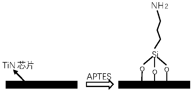
本发明涉及生物芯片制备技术领域,尤其涉及一种用于TiN芯片合成核酸的表面连接体及其制备方法和应用。The invention relates to the technical field of biochip preparation, in particular to a surface linker used for TiN chip synthesis of nucleic acid, a preparation method and application thereof.
半导体芯片合成核酸的稳定连接体(linker)非常重要,其可用于表面原位合成或预制备大量的DNA探针,同时也可牢固连接核酸以便进行后续的原位杂交等应用,通过对样品杂交信号的检测分析,得到样品的遗传信息(基因序列及表达的信息)。可在疾病诊断、药物筛选和新药开发、农业与环境研究等领域发挥巨大的应用。现在市场多用贵金属芯片合成核酸,其方法众多,包括多种linker和多种核酸合成方法。但用于半导体芯片合成核酸的稳定linker很是罕见。由于半导体价格便宜,芯片制备简单,且更加适合工业化大批量生产,因此开发半导体芯片linker,促进半导体芯片的应用非常重要。现在多是在半导体上简单修饰分子后连接聚合物或嫁接其他材料,如Y.Shacham-Diamand研究了用化学方法在TiN上修饰硅烷化分子后再镀Co(W,P)材料[1];Xuan Tuan Le用重氮盐法修饰TiN表面,再用于电镀聚合物[2],此方法问题在于需要加电修饰,不利于规模化大批量生产;另一种方法是利用直接吸附法,将小分子吸附在TiN表面,以此来应用[3],此方法的缺点在于粘附性不牢固,对水敏感,特别在后续应用时会脱落,难以进一步开发所需的芯片诊断产品。The stable linker (linker) of nucleic acid synthesized by semiconductor chip is very important. It can be used for surface in situ synthesis or pre-preparation of a large number of DNA probes, and it can also be firmly connected to nucleic acid for subsequent in situ hybridization and other applications. Signal detection and analysis, to obtain the genetic information of the sample (gene sequence and expression information). It can play a huge role in disease diagnosis, drug screening and new drug development, agricultural and environmental research and other fields. Nowadays, precious metal chips are often used to synthesize nucleic acids in the market, and there are many methods, including various linkers and various nucleic acid synthesis methods. However, stable linkers for the synthesis of nucleic acids on semiconductor chips are rare. Because semiconductors are cheap, chip preparation is simple, and they are more suitable for industrial mass production, it is very important to develop semiconductor chip linkers to promote the application of semiconductor chips. Now most of them are simply modifying molecules on semiconductors and then connecting polymers or grafting other materials. For example, Y. Shacham-Diamand has studied chemical methods to modify silanized molecules on TiN and then plate Co(W,P) materials[1]; Xuan Tuan Le modified the surface of TiN with diazonium salt method, and then used it for electroplating polymer[2]. Small molecules are adsorbed on the surface of TiN for application[3]. The disadvantage of this method is that the adhesion is not strong, it is sensitive to water, and it will fall off especially in subsequent applications, making it difficult to further develop the required chip diagnostic products.
发明内容Contents of the invention
有鉴于此,本发明提供了一种用于半导体TiN芯片合成核酸的稳定连接体(linker),其主要方法是在洁净的TiN表面进行硅烷化反应,使表面氨基化,再通过羧基氨基反应修饰上含有羟基/羟基保护基和酯基的功能化分子,便可实现后续芯片上核酸原位合成。In view of this, the present invention provides a kind of stable linker (linker) that is used for semiconductor TiN chip synthesis nucleic acid, and its main method is to carry out silanization reaction on clean TiN surface, make surface amination, then modify by carboxyl amino reaction Functionalized molecules containing hydroxyl/hydroxyl protecting groups and ester groups can realize subsequent in situ synthesis of nucleic acids on the chip.
一方面,本发明提供了一种芯片表面连接体,其特征在于,所述连接体通过硅烷化分子与芯片表面反应形成连接在芯片表面的键合分子,所述键合分子进一步与功能化分子反应修饰上羟基和酯基制得。具体地,本发明提供了一种芯片表面连接体,所述连接体通过 硅烷化分子于合适溶剂中与芯片表面反应形成连接在芯片表面的键合分子,所述键合分子与功能化分子反应修饰上羟基和酯基制得。所述羟基可以是游离的羟基也可以是被保护基保护的羟基。On the one hand, the present invention provides a chip surface connector, characterized in that, the connector reacts with the chip surface through silanization molecules to form bonding molecules connected to the chip surface, and the bonding molecules are further combined with functionalized molecules Reaction modified on the hydroxyl and ester in the system. Specifically, the present invention provides a chip surface connector, which reacts with the chip surface through silanization molecules in a suitable solvent to form bonding molecules connected to the chip surface, and the bonding molecules react with the functionalized molecules Modified on the hydroxyl and ester in the system. The hydroxyl group can be a free hydroxyl group or a hydroxyl group protected by a protecting group.
在一些实施方案中,所述硅烷化分子选自3-氨丙基三乙氧基硅烷、十二烷基三甲氧基硅烷、乙烯基三乙氧基硅烷、双(γ-三甲基甲硅烷基丙基)胺和γ-(2,3-环氧丙氧基)丙基三甲氧基硅烷中的一种或多种,优选为3-氨丙基三乙氧基硅烷。In some embodiments, the silylated molecule is selected from the group consisting of 3-aminopropyltriethoxysilane, dodecyltrimethoxysilane, vinyltriethoxysilane, bis(γ-trimethylsilane One or more of propyl)amine and γ-(2,3-glycidoxy)propyltrimethoxysilane, preferably 3-aminopropyltriethoxysilane.
在一些实施方案中,所述硅烷化分子是在合适的溶剂中与芯片表面进行反应的。在一些实施方案中,所述溶剂选自甲苯、乙醇和甲醇中的一种或多种,优选为甲苯。In some embodiments, the silylated molecules are reacted with the chip surface in a suitable solvent. In some embodiments, the solvent is selected from one or more of toluene, ethanol and methanol, preferably toluene.
在一些实施方案中,所述溶剂与硅烷化分子的体积比为2:1~40:1,优选为20:1~35:1,更优选为30:1。所述溶剂与硅烷化分子的体积比可选自2:1、3:1、4:1、5:1、6:1、7:1、8:1、9:1、10:1、11:1、12:1、13:1、14:1、15:1、16:1、17:1、18:1、19:1、20:1、21:1、22:1、23:1、24:1、25:1、26:1、27:1、28:1、29:1、30:1、31:1、32:1、33:1、34:1、35:1、36:1、37:1、38:1、39:1或40:1。In some embodiments, the volume ratio of the solvent to the silylated molecules is 2:1-40:1, preferably 20:1-35:1, more preferably 30:1. The volume ratio of the solvent to the silylated molecules may be selected from 2:1, 3:1, 4:1, 5:1, 6:1, 7:1, 8:1, 9:1, 10:1, 11 :1, 12:1, 13:1, 14:1, 15:1, 16:1, 17:1, 18:1, 19:1, 20:1, 21:1, 22:1, 23:1 , 24:1, 25:1, 26:1, 27:1, 28:1, 29:1, 30:1, 31:1, 32:1, 33:1, 34:1, 35:1, 36 :1, 37:1, 38:1, 39:1, or 40:1.
在一些实施方案中,所述硅烷化分子与芯片表面反应时的温度为50℃~100℃,优选60℃~80℃,更优选65℃。所述反应的具体反应温度可选自50℃、51℃、52℃、53℃、54℃、55℃、56℃、57℃、58℃、59℃、60℃、61℃、62℃、63℃、64℃、65℃、66℃、67℃、68℃、69℃、70℃、71℃、72℃、73℃、74℃、75℃、76℃、77℃、78℃、79℃、80℃、81℃、82℃、83℃、84℃、85℃、86℃、87℃、88℃、89℃、90℃、91℃、92℃、93℃、94℃、95℃、96℃、97℃、98℃、99℃或100℃。在一些实施方案中,所述硅烷化分子与芯片表面反应时间优选1~6小时,更优选2~5小时,最优选4小时。其他优选的反应时间为1小时、1.5小时、2小时、2.5小时、3小时、3.5小时、4小时、4.5小时、5小时、5.5小时或6小时。在一些实施方案中,所述硅烷化分子与芯片表面反应条件是在50℃~100℃反应1~6小时。在一些优选实施方案中,所述硅烷化分子与芯片表面反应条件是在60℃~80℃反应2~5小时。在一个具体实施方案中,所述硅烷化分子与芯片表面反应条件是在65℃密封反应4小时。In some embodiments, the temperature at which the silylated molecules react with the surface of the chip is 50°C to 100°C, preferably 60°C to 80°C, more preferably 65°C. The specific reaction temperature of the reaction can be selected from 50°C, 51°C, 52°C, 53°C, 54°C, 55°C, 56°C, 57°C, 58°C, 59°C, 60°C, 61°C, 62°C, 63°C ℃, 64℃, 65℃, 66℃, 67℃, 68℃, 69℃, 70℃, 71℃, 72℃, 73℃, 74℃, 75℃, 76℃, 77℃, 78℃, 79℃, 80°C, 81°C, 82°C, 83°C, 84°C, 85°C, 86°C, 87°C, 88°C, 89°C, 90°C, 91°C, 92°C, 93°C, 94°C, 95°C, 96°C , 97°C, 98°C, 99°C or 100°C. In some embodiments, the reaction time between the silylated molecules and the surface of the chip is preferably 1-6 hours, more preferably 2-5 hours, most preferably 4 hours. Other preferred reaction times are 1 hour, 1.5 hours, 2 hours, 2.5 hours, 3 hours, 3.5 hours, 4 hours, 4.5 hours, 5 hours, 5.5 hours or 6 hours. In some embodiments, the conditions for the reaction of the silylated molecules with the surface of the chip are at 50° C. to 100° C. for 1 to 6 hours. In some preferred embodiments, the conditions for the reaction of the silylated molecules with the surface of the chip are at 60° C. to 80° C. for 2 to 5 hours. In a specific embodiment, the conditions for the reaction between the silylated molecules and the surface of the chip are sealing reaction at 65° C. for 4 hours.
在一些实施方案中,所述功能化分子为包含长碳链且含有酯基的羟基物质。在另一些实施方案中,所述功能化分子选自丁二酸酐修饰的碱基单体、甲基丙烯酸羟乙酯、丁二酸修饰的碱基单体和乙二酸修饰的碱基单体中的一种或多种,优选为丁二酸酐修饰的碱基单体。在一些实施方案中,所述功能化分子的碱基单体部分选自腺嘌呤核苷、鸟嘌呤核苷、胞嘧啶核苷、胸腺嘧啶核苷和尿嘧啶核苷中的一种或多种。在一个具体实施方案中,所述 功能化分子选自丁二酸酐修饰的腺嘌呤核苷、鸟嘌呤核苷、胞嘧啶核苷、胸腺嘧啶核苷和尿嘧啶核苷中的一种或多种。In some embodiments, the functionalized molecule is a hydroxyl species comprising a long carbon chain and containing an ester group. In other embodiments, the functionalized molecule is selected from the group consisting of succinic anhydride modified base monomers, hydroxyethyl methacrylate, succinic acid modified base monomers and oxalic acid modified base monomers One or more of them are preferably succinic anhydride-modified base monomers. In some embodiments, the base monomer portion of the functionalized molecule is selected from one or more of adenosine, guanosine, cytidine, thymidine and uridine . In a specific embodiment, the functionalized molecule is selected from one or more of succinic anhydride-modified adenosine, guanosine, cytidine, thymidine and uridine .
在一些实施方案中,在用功能化分子反应修饰键合分子之前,还包括在合适条件下加固芯片表面连接键合分子的步骤。In some embodiments, before modifying the bonding molecules with the functionalized molecules, a step of strengthening the bonding molecules on the surface of the chip under suitable conditions is further included.
在一些实施方案中,所述加固条件为放置于60℃~100℃干燥装置中1小时~6小时,优选加固放置温度为75℃~95℃,最优选90℃。其他优选的加固放置温度为75℃、76℃、77℃、78℃、79℃、80℃、81℃、82℃、83℃、84℃、85℃、86℃、87℃、88℃、89℃、90℃、91℃、92℃、93℃、94℃或95℃;加固放置时间优选为1小时~4小时,最优选1小时,其他优选的放置时间为1小时、1.5小时、2小时、2.5小时、3小时、3.5小时或4小时。在一些具体实施方案中,所述加固条件为放置于90℃干燥装置中1小时。In some embodiments, the strengthening condition is placed in a drying device at 60°C to 100°C for 1 hour to 6 hours, preferably the strengthening temperature is 75°C to 95°C, most preferably 90°C. Other preferred reinforcement placement temperatures are 75°C, 76°C, 77°C, 78°C, 79°C, 80°C, 81°C, 82°C, 83°C, 84°C, 85°C, 86°C, 87°C, 88°C, 89°C °C, 90 °C, 91 °C, 92 °C, 93 °C, 94 °C or 95 °C; the time for reinforcement is preferably 1 hour to 4 hours, most preferably 1 hour, and other preferred placement times are 1 hour, 1.5 hours, or 2 hours , 2.5 hours, 3 hours, 3.5 hours, or 4 hours. In some specific embodiments, the strengthening condition is placed in a drying device at 90° C. for 1 hour.
在一些实施方案中,所述芯片为半导体芯片。在一些具体实施方案中,所述半导体芯片表面包含TiN(氮化钛)或TiW(钛钨),优选TiN。In some embodiments, the chip is a semiconductor chip. In some embodiments, the surface of the semiconductor chip comprises TiN (titanium nitride) or TiW (titanium tungsten), preferably TiN.
另一方面,本发明还提供一种芯片表面连接体的制备方法,包括以下步骤:On the other hand, the present invention also provides a method for preparing a chip surface connector, comprising the following steps:
步骤1:将硅烷化分子与合适溶剂按一定体积比混合得到混合液;Step 1: Mix the silanized molecules with a suitable solvent in a certain volume ratio to obtain a mixed solution;
步骤2:将芯片与步骤1的混合液接触反应形成连接在芯片表面的键合分子;Step 2: contacting the chip with the mixed solution in step 1 to form bonding molecules attached to the surface of the chip;
步骤3:将反应后连接键合分子的芯片表面与功能化分子接触反应修饰上羟基和酯基。Step 3: After the reaction, the surface of the chip connected with the bonding molecule is contacted with the functionalized molecule to modify the hydroxyl group and the ester group.
在一些实施方案中,上述步骤1中所述硅烷化分子选自3-氨丙基三乙氧基硅烷、十二烷基三甲氧基硅烷、乙烯基三乙氧基硅烷、双(γ-三甲基甲硅烷基丙基)胺和γ-(2,3-环氧丙氧基)丙基三甲氧基硅烷中的一种或多种,优选为3-氨丙基三乙氧基硅烷。In some embodiments, the silylated molecule in step 1 above is selected from 3-aminopropyltriethoxysilane, dodecyltrimethoxysilane, vinyltriethoxysilane, bis(γ-triethoxysilane, One or more of methylsilylpropyl)amine and γ-(2,3-glycidoxy)propyltrimethoxysilane, preferably 3-aminopropyltriethoxysilane.
在一些实施方案中,上述步骤1中所述溶剂选自甲苯、乙醇和甲醇中的一种或多种,优选为甲苯。In some embodiments, the solvent in step 1 above is selected from one or more of toluene, ethanol and methanol, preferably toluene.
在一些实施方案中,上述步骤1中所述溶剂与硅烷化分子的体积比为2:1~40:1,优选20:1~35:1,更优选30:1。其他优选的溶剂与硅烷化分子的体积比为2:1、3:1、4:1、5:1、6:1、7:1、8:1、9:1、10:1、11:1、12:1、13:1、14:1、15:1、16:1、17:1、18:1、19:1、20:1、21:1、22:1、23:1、24:1、25:1、26:1、27:1、28:1、29:1、30:1、31:1、32:1、33:1、34:1、35:1、36:1、37:1、38:1、39:1或40:1。In some embodiments, the volume ratio of the solvent to the silylated molecules in the above step 1 is 2:1-40:1, preferably 20:1-35:1, more preferably 30:1. Other preferred volume ratios of solvent to silylated molecules are 2:1, 3:1, 4:1, 5:1, 6:1, 7:1, 8:1, 9:1, 10:1, 11: 1, 12:1, 13:1, 14:1, 15:1, 16:1, 17:1, 18:1, 19:1, 20:1, 21:1, 22:1, 23:1, 24:1, 25:1, 26:1, 27:1, 28:1, 29:1, 30:1, 31:1, 32:1, 33:1, 34:1, 35:1, 36: 1, 37:1, 38:1, 39:1, or 40:1.
在一些实施方案中,上述步骤2中所述硅烷化分子与芯片表面反应的条件为50℃~100℃反应1~6小时。在一些优选实施方案中,所述硅烷化分子与芯片表面反应的条件为60℃~80℃反应2~5小时。在一个具体实施方案中,所述硅烷化分子与芯片表面反应的条件为65℃密封反应4小时。In some embodiments, the conditions for the reaction of the silylated molecules with the surface of the chip in step 2 above are 50° C. to 100° C. for 1 to 6 hours. In some preferred embodiments, the conditions for the reaction of the silylated molecules with the surface of the chip are 60° C. to 80° C. for 2 to 5 hours. In a specific embodiment, the conditions for the reaction of the silylated molecules with the surface of the chip are sealing reaction at 65° C. for 4 hours.
在一些实施方案中,所述功能化分子为包含长碳链且含有酯基的羟基物质。在另一些实施方案中,所述功能化分子选自丁二酸酐修饰的碱基单体、甲基丙烯酸羟乙酯、丁二酸修饰的碱基单体和乙二酸修饰的碱基单体一种或多种,优选为丁二酸酐修饰的碱基单体。在一些实施方案中,所述功能化分子中的碱基单体部分选自腺嘌呤核苷、鸟嘌呤核苷、胞嘧啶核苷、胸腺嘧啶核苷和尿嘧啶核苷中的一种或多种。在一个具体实施方案中,所述功能化分子选自丁二酸酐修饰的腺嘌呤核苷、鸟嘌呤核苷、胞嘧啶核苷、胸腺嘧啶核苷和尿嘧啶核苷中的一种或多种。In some embodiments, the functionalized molecule is a hydroxyl species comprising a long carbon chain and containing an ester group. In other embodiments, the functionalized molecule is selected from the group consisting of succinic anhydride modified base monomers, hydroxyethyl methacrylate, succinic acid modified base monomers and oxalic acid modified base monomers One or more, preferably succinic anhydride-modified base monomers. In some embodiments, the base monomer part in the functionalized molecule is selected from one or more of adenosine, guanosine, cytidine, thymidine and uridine kind. In a specific embodiment, the functionalized molecule is selected from one or more of succinic anhydride-modified adenosine, guanosine, cytidine, thymidine and uridine .
在一些实施方案中,所述步骤3之前还包括在合适条件下加固芯片表面连接键合分子的步骤。In some embodiments, before step 3, a step of strengthening the bonding molecules connected to the surface of the chip under suitable conditions is also included.
在一些实施方案中,所述加固条件为放置于60℃~100℃干燥装置中1小时~6小时,优选为放置于75℃~95℃干燥装置中1小时~3小时,最优选为放置于90℃干燥装置中1小时。所述加固条件的放置温度可选自75℃、76℃、77℃、78℃、79℃、80℃、81℃、82℃、83℃、84℃、85℃、86℃、87℃、88℃、89℃、90℃、91℃、92℃、93℃、94℃或95℃;加固放置时间优选为1小时~4小时,最优选为1小时,其他优选的放置时间可选自1小时、1.5小时、2小时、2.5小时、3小时、3.5小时或4小时。在一些具体实施方案中,所述加固条件为放置于90℃干燥装置中1小时。In some embodiments, the reinforcement condition is placed in a drying device at 60°C to 100°C for 1 hour to 6 hours, preferably placed in a drying device at 75°C to 95°C for 1 hour to 3 hours, most preferably placed in a 90°C drying unit for 1 hour. The storage temperature of the reinforcement condition can be selected from 75°C, 76°C, 77°C, 78°C, 79°C, 80°C, 81°C, 82°C, 83°C, 84°C, 85°C, 86°C, 87°C, 88°C °C, 89 °C, 90 °C, 91 °C, 92 °C, 93 °C, 94 °C or 95 °C; the time for strengthening and placing is preferably 1 hour to 4 hours, most preferably 1 hour, and other preferred placing times can be selected from 1 hour , 1.5 hours, 2 hours, 2.5 hours, 3 hours, 3.5 hours or 4 hours. In some specific embodiments, the strengthening condition is placed in a drying device at 90° C. for 1 hour.
在一些实施方案中,所述芯片为半导体芯片。在一些具体实施方案中,所述半导体芯片表面包含TiN或TiW,优选TiN。In some embodiments, the chip is a semiconductor chip. In some specific embodiments, the surface of the semiconductor chip comprises TiN or TiW, preferably TiN.
本发明还提供前文所述的芯片表面连接体在核酸合成或制备芯片诊断试剂盒中的应用。The present invention also provides the application of the aforementioned chip surface linker in nucleic acid synthesis or preparation of a chip diagnostic kit.
发明详述Detailed description of the invention
本发明提供了一种芯片表面连接体,特别是半导体芯片连接体,所述连接体通过硅烷化分子于合适溶剂中与芯片表面反应形成连接在芯片表面的键合分子,并与功能化分子反应修饰羟基和酯基制得。The invention provides a chip surface connector, especially a semiconductor chip connector, the connector reacts with the chip surface through silanization molecules in a suitable solvent to form bonding molecules connected to the chip surface, and reacts with functionalized molecules Modified hydroxyl and ester obtained.
本发明描述的硅烷化分子可以是3-氨丙基三乙氧基硅烷、十二烷基三甲氧基硅烷、乙烯基三乙氧基硅烷、双(γ-三甲基甲硅烷基丙基)胺或γ-(2,3-环氧丙氧基)丙基三甲氧基硅烷。在本发明的一些实施方案中,硅烷化分子为3-氨丙基三乙氧基硅烷。本发明中描述的键合分子是硅烷化分子与芯片表面发生反应后得到的共价连接在芯片表面的基团。在本发明的一些实施方案中,所述硅烷化分子APTES(3-氨丙基三乙氧基硅烷)溶解在如甲苯等 合适溶剂中(溶剂与硅烷化分子体积比为2:1~40:1,优选30:1),于50℃~100℃(优选65℃)的高温下与含TiN的半导体芯片表面反应1~6小时(优选4小时)后,于芯片表面形成键合分子。The silylated molecules described in this invention can be 3-aminopropyltriethoxysilane, dodecyltrimethoxysilane, vinyltriethoxysilane, bis(γ-trimethylsilylpropyl) Amine or γ-(2,3-Glycidoxy)propyltrimethoxysilane. In some embodiments of the invention, the silylated molecule is 3-aminopropyltriethoxysilane. The bonding molecule described in the present invention is a group covalently linked to the chip surface obtained after the silylated molecule reacts with the chip surface. In some embodiments of the present invention, the silylated molecule APTES (3-aminopropyltriethoxysilane) is dissolved in a suitable solvent such as toluene (the volume ratio of solvent to silylated molecule is 2:1-40: 1, preferably 30:1), after reacting with the surface of a TiN-containing semiconductor chip at a high temperature of 50°C to 100°C (preferably 65°C) for 1 to 6 hours (preferably 4 hours), the bonding molecules are formed on the chip surface.
在本发明的一些实施方案中,在用功能化分子反应修饰键合分子之前,还包括在合适条件下加固芯片表面连接键合分子的步骤。在本发明的一些实施方案中,加固条件为将与硅烷化分子反应后的芯片放置于60℃~100℃的烘箱1~6小时,优选90℃的烘箱中放置1小时。In some embodiments of the present invention, before modifying the bonding molecules with the functionalized molecules, a step of strengthening the bonding molecules connected to the surface of the chip under suitable conditions is also included. In some embodiments of the present invention, the reinforcement condition is to place the chip after reacting with the silylated molecules in an oven at 60° C. to 100° C. for 1 to 6 hours, preferably in an oven at 90° C. for 1 hour.
本发明中功能化分子为包含长碳链且含有酯基的羟基物质,可以是丁二酸酐修饰的碱基单体、甲基丙烯酸羟乙酯、丁二酸修饰的碱基单体或乙二酸修饰的碱基单体,在本发明的一些实施方案中使用丁二酸酐修饰的腺嘌呤核苷、鸟嘌呤核苷、胞嘧啶核苷或胸腺嘧啶核苷中一种或多种混合溶液。本发明所述长碳链是指分子中包含有多个碳碳共价键的长链结构,可包含碳原子数为2个以上,优选为2~4个。包含长碳链且含有酯基的羟基物质分子结构越长,后续在核酸合成过程中空间位阻越小,有利于合成。在本发明的一些实施方案中单独使用丁二酸酐修饰的腺嘌呤核苷、丁二酸酐修饰的鸟嘌呤核苷、丁二酸酐修饰的胞嘧啶核苷或丁二酸酐修饰的胸腺嘧啶核苷溶液。在一些实施方案中,所述功能化分子还可选自丁二酸酐修饰的腺嘌呤核苷、鸟嘌呤核苷、胞嘧啶核苷、胸腺嘧啶核苷或尿嘧啶核苷,甲基丙烯酸羟乙酯,丁二酸修饰的腺嘌呤核苷、鸟嘌呤核苷、胞嘧啶核苷、胸腺嘧啶核苷或尿嘧啶核苷,乙二酸修饰的腺嘌呤核苷、鸟嘌呤核苷、胞嘧啶核苷、胸腺嘧啶核苷或尿嘧啶核苷中羧酸与氨基反应后脱除羟基的基团。本发明中将功能分子修饰于键合分子上,形成的功能化分子基团含有羟基和酯基,便于后续芯片上电促DNA的合成以及切割。In the present invention, the functional molecule is a hydroxyl substance containing a long carbon chain and an ester group, which can be a base monomer modified by succinic anhydride, hydroxyethyl methacrylate, a base monomer modified by succinic acid, or ethylene glycol Acid-modified base monomers, in some embodiments of the present invention, a mixed solution of one or more of succinic anhydride-modified adenosine, guanosine, cytidine or thymidine is used. The long carbon chain in the present invention refers to a long chain structure containing multiple carbon-carbon covalent bonds in the molecule, which may contain more than 2 carbon atoms, preferably 2 to 4 carbon atoms. The longer the molecular structure of hydroxyl substances containing long carbon chains and ester groups, the smaller the steric hindrance in the subsequent nucleic acid synthesis process, which is beneficial to the synthesis. In some embodiments of the present invention, a solution of succinic anhydride-modified adenosine, succinic anhydride-modified guanosine, succinic anhydride-modified cytidine or succinic anhydride-modified thymidine is used alone . In some embodiments, the functionalized molecule can also be selected from succinic anhydride-modified adenosine, guanosine, cytidine, thymidine or uridine, hydroxyethyl methacrylate Esters, succinate-modified adenosine, guanosine, cytosine, thymidine or uridine, oxalate-modified adenosine, guanosine, cytosine The group that removes the hydroxyl group after the carboxylic acid in glycoside, thymidine or uridine reacts with the amino group. In the present invention, the functional molecules are modified on the bonding molecules, and the formed functional molecular groups contain hydroxyl groups and ester groups, which is convenient for the synthesis and cleavage of electrocatalyzed DNA on the subsequent chip.
本发明中功能化分子反应修饰的羟基可以是羟基基团本身,即-OH,也可以是被保护的羟基,如-ODMT,羟基保护基是通过常用的保护基团保护的羟基。本发明的一些实施方案中,所述功能化分子反应修饰的羟基为羟基基团。在另一些实施方案中,所述功能化分子反应修饰的羟基为ODMT。In the present invention, the hydroxyl group modified by the functionalized molecular reaction can be the hydroxyl group itself, ie -OH, or a protected hydroxyl group, such as -ODMT, and the hydroxyl protecting group is a hydroxyl group protected by a commonly used protecting group. In some embodiments of the present invention, the hydroxyl group modified by the reaction of the functionalized molecule is a hydroxyl group. In other embodiments, the reactively modified hydroxyl group of the functionalized molecule is ODMT.
本发明描述的芯片表面连接体通过共价键稳定结合在芯片表面,可用于电辅助芯片合成核酸等应用。其中,所述的半导体芯片为本领域常见的包括半导体材料的芯片。本发明中所述半导体芯片可选自一般表面包含TiN或TiW的片状半导体芯片。本发明的一个具体实施方案中,所述芯片为可应用于CustomArray芯片合成仪的半导体芯片。在进行芯片表面连接反应前包括芯片的清洗步骤。在本发明中,所述芯片清洗步骤可包括依次用水、醇、水 冲洗,干燥,即得干燥清洁的芯片表面。其中,所述水一般为蒸馏水,醇为乙醇、甲醇,主要去除污染物质如其他杂质金属粉尘、无机颗粒和有机小分子。The chip surface linker described in the present invention is stably bound on the chip surface through a covalent bond, and can be used in applications such as electrically assisting the chip to synthesize nucleic acids. Wherein, the semiconductor chip is a common chip including semiconductor material in the field. The semiconductor chip in the present invention can be selected from sheet semiconductor chips generally whose surface contains TiN or TiW. In a specific embodiment of the present invention, the chip is a semiconductor chip applicable to a CustomArray chip synthesizer. A chip cleaning step is included before performing the chip surface ligation reaction. In the present invention, the chip cleaning step may include sequentially washing with water, alcohol, and water, and drying, so as to obtain a dry and clean chip surface. Wherein, the water is generally distilled water, and the alcohol is ethanol or methanol, which mainly removes pollutants such as other impurities, metal dust, inorganic particles and small organic molecules.
本发明还提供一种芯片表面连接体的制备方法,包括以下步骤:将硅烷化分子与合适溶剂按一定体积比混合得到混合液;将清洗后的芯片与配好的混合液接触反应形成连接在芯片表面的键合分子;将反应后的芯片表面与功能化分子接触反应修饰上羟基和酯基制得连接体。在一些实施方案中,在用功能化分子反应修饰键合分子之前还包括在合适条件下加固芯片表面连接键合分子的步骤。The present invention also provides a method for preparing a chip surface connector, which includes the following steps: mixing silanized molecules with a suitable solvent in a certain volume ratio to obtain a mixed solution; contacting and reacting the cleaned chip with the prepared mixed solution to form a connection in the Bonding molecules on the chip surface; the reacted chip surface is contacted with functionalized molecules to modify hydroxyl groups and ester groups to obtain linkers. In some embodiments, before modifying the bonding molecules with the functionalized molecules, a step of strengthening the chip surface to connect the bonding molecules under suitable conditions is also included.
在本发明的一些实施例中,以甲苯为溶剂与硅烷化分子按体积比2:1~40:1,优选30:1混合制得混合液。所述硅烷化分子可以是3-氨丙基三乙氧基硅烷、十二烷基三甲氧基硅烷、乙烯基三乙氧基硅烷、双(γ-三甲基甲硅烷基丙基)胺或γ-(2,3-环氧丙氧基)丙基三甲氧基硅烷,优选3-氨丙基三乙氧基硅烷。将清洗后的芯片与所述混合液在50℃~100℃条件,优选65℃条件下反应1~6小时,优选反应4小时。具体反应如下所示:In some embodiments of the present invention, toluene is used as a solvent and the silylated molecules are mixed in a volume ratio of 2:1-40:1, preferably 30:1 to prepare a mixed solution. The silylated molecule can be 3-aminopropyltriethoxysilane, dodecyltrimethoxysilane, vinyltriethoxysilane, bis(γ-trimethylsilylpropyl)amine or γ-(2,3-Glycidoxy)propyltrimethoxysilane, preferably 3-aminopropyltriethoxysilane. The cleaned chip is reacted with the mixed solution at 50° C. to 100° C., preferably at 65° C., for 1 to 6 hours, preferably 4 hours. The specific reaction is as follows:
反应后,取出芯片,再依次用水、醇冲洗,最后用水冲洗,吹干。After the reaction, take out the chip, rinse it with water and alcohol in turn, and finally rinse it with water and dry it.
将反应后的芯片在合适条件下加固芯片表面连接的键合分子。所述的加固条件为放置于60℃~100℃干燥装置中加固1小时~6小时,优选加固放置温度为75℃~95℃,最优选为90℃;加固放置时间优选为1小时~4小时,最优选为1小时。在本发明中所述加固芯片的温度一般会高于芯片表面连接硅烷化分子的温度。The reacted chip is under suitable conditions to strengthen the bonding molecules connected to the surface of the chip. The reinforcement conditions are placed in a drying device at 60°C to 100°C for 1 hour to 6 hours, preferably the temperature for reinforcement is 75°C to 95°C, most preferably 90°C; the time for reinforcement is preferably 1 hour to 4 hours , most preferably 1 hour. In the present invention, the temperature of the reinforced chip is generally higher than the temperature of the silanized molecules attached to the surface of the chip.
加固后的芯片再进行功能化分子修饰。功能化分子为包含长碳链且含有酯基的羟基物质,所述羟基物质包括但不限于丁二酸酐修饰的碱基单体、甲基丙烯酸羟乙酯、乙二酸修饰的碱基单体。在本发明的一些实施方案中单独使用丁二酸酐修饰的腺嘌呤核苷、鸟嘌呤核苷、胞嘧啶核苷、胸腺嘧啶核苷或尿嘧啶核苷的溶液。在本发明的一些具体实施方案中使用丁二酸酐修饰的腺嘌呤核苷、鸟嘌呤核苷、胞嘧啶核苷、胸腺嘧啶核苷和尿嘧啶核苷的两种或两种以上混合溶液。功能化分子中含有酯基,可用于DNA合成及切割,所述的酯基是切割位点,为了把芯片上合成的DNA切下来,成自由溶液状的寡核苷酸池(oligo pool)。功能化分子中的含有的羟基是DNA合成的启动位点。在本发明的一些实施方案中,碱基单体部分提供的羟基用于DNA合成。另外,所述羟基分子溶液还可包含用于功能化修饰的活 化剂等,例如NHS(N,N-羟基琥珀酰亚胺)、EDC(1-(3-二甲氨基丙基)-3-乙基碳二亚胺盐酸盐)。The reinforced chip is then modified with functional molecules. Functionalized molecules are hydroxyl species containing long carbon chains and ester groups, including but not limited to succinic anhydride-modified base monomers, hydroxyethyl methacrylate, oxalic acid-modified base monomers . Solutions of succinic anhydride-modified adenosine, guanosine, cytidine, thymidine or uridine are used alone in some embodiments of the invention. In some embodiments of the present invention, two or more mixed solutions of succinic anhydride-modified adenosine, guanosine, cytidine, thymidine and uridine are used. The functionalized molecule contains an ester group, which can be used for DNA synthesis and cleavage. The ester group is the cleavage site. In order to cut off the DNA synthesized on the chip, it forms a free solution-like oligonucleotide pool (oligo pool). The hydroxyl group contained in the functionalized molecule is the initiation site for DNA synthesis. In some embodiments of the invention, the hydroxyl groups provided by the base monomer moiety are used for DNA synthesis. In addition, the hydroxyl molecule solution may also contain activators for functional modification, such as NHS (N,N-hydroxysuccinimide), EDC (1-(3-dimethylaminopropyl)-3- ethylcarbodiimide hydrochloride).
本发明还提供如前文所述的芯片表面连接体在合成DNA或制备芯片试剂盒中的应用。本发明的芯片表面连接体包含如下应用:在芯片上进行DNA合成;用于疾病生物标志物芯片检测;用于开发POCT的芯片试剂盒;高通量芯片筛选试剂盒。The present invention also provides the application of the above-mentioned chip surface linker in synthesizing DNA or preparing a chip kit. The chip surface connector of the present invention includes the following applications: DNA synthesis on the chip; chip detection of disease biomarkers; chip kit for developing POCT; high-throughput chip screening kit.
本发明中的芯片表面连接体能用于合成DNA;合成的DNA与寡核苷酸(如DNA引物)杂交后再经碱和热TE处理,还可用于与寡核苷酸(如DNA引物)杂交。本发明的芯片表面连接体合成的DNA经过多次核酸杂交、洗脱、杂交循环应用,该芯片表面连接体依然能保持较好的稳定性。本发明实施例制备的芯片表面连接体导电性好,加电稳定,可用于电辅助合成DNA等核酸分子,如连接体没有此性质会影响DNA合成。本发明的芯片表面连接体抗DNA合成所需的有机溶剂(包括4,5-二氰基咪唑,三氯乙酸,乙酸酐,1-甲基咪唑及碘液等),抗酸碱,抗氨解,否则无法进行DNA合成。在芯片连接体用于芯片杂交检测应用中,本发明可解决现有连接体对水、酸碱、有机溶剂的合成环境敏感、对热不稳定等问题,因此芯片可以重复性利用。The chip surface linker among the present invention can be used for synthesizing DNA; After the hybridization of synthetic DNA and oligonucleotide (as DNA primer) after alkali and thermal TE treatment, also can be used for hybridizing with oligonucleotide (as DNA primer) . The DNA synthesized by the linker on the chip surface of the present invention can still maintain good stability after multiple cycles of nucleic acid hybridization, elution and hybridization. The chip surface linker prepared in the embodiment of the present invention has good conductivity and is stable when powered on, and can be used for electrically assisted synthesis of nucleic acid molecules such as DNA. If the linker does not have this property, DNA synthesis will be affected. The chip surface linker of the present invention is resistant to organic solvents required for DNA synthesis (including 4,5-dicyanoimidazole, trichloroacetic acid, acetic anhydride, 1-methylimidazole and iodine solution, etc.), acid and alkali resistance, and ammonia resistance. solution, otherwise DNA synthesis cannot be performed. In the application of the chip linker for chip hybridization detection, the present invention can solve the problems that the existing linker is sensitive to the synthetic environment of water, acid-base, and organic solvent, unstable to heat, etc., so the chip can be used repeatedly.
术语“芯片”表示由半导体之类的无机物或金、银、铂等金属形成的固体支持物,其表面具有特定位点形成的微阵列,所述位点通常以行列形式排列,其中各位点可用于某种类型的化学或生物化学分析、合成或方法。微阵列上的这些位点通常小于100微米。在本发明的一些实施方案中,所述芯片为含TiN的半导体芯片。The term "chip" refers to a solid support formed of inorganic substances such as semiconductors or metals such as gold, silver, platinum, etc., and its surface has a microarray formed by specific sites, and the sites are usually arranged in rows and columns, wherein each site Can be used in some type of chemical or biochemical analysis, synthesis or method. These sites on the microarray are typically smaller than 100 microns. In some embodiments of the invention, the chip is a TiN-containing semiconductor chip.
术语“键合分子”表示位于连接体端部,分子的一端能与固体表面(如含TiN的半导体芯片)共价相连,另一端具有反应基团的化学分子,所述反应基团与或能与相关的化学物质,例如小分子、寡聚物或聚合物相连,在本发明中能与功能化分子相连。键合分子已经与固体表面结合和/或其反应基团已连接有相关的化学物质。键合分子的反应基团可连接有保护基团,其中所述保护基团可用化学或电化学方法除去。The term "bonding molecule" refers to a chemical molecule located at the end of a linker, one end of which can be covalently bonded to a solid surface (such as a TiN-containing semiconductor chip), and the other end has a reactive group that interacts with or can Linkage to relevant chemical species, such as small molecules, oligomers or polymers, can be linked to functionalized molecules in the present invention. Bonding molecules have been bound to a solid surface and/or their reactive groups have associated chemicals attached to them. The reactive groups of the bonding molecules may have attached protecting groups, wherein the protecting groups may be removed chemically or electrochemically.
术语“功能化分子”表示位于连接体末端部分,基团的一端能与键合分子相连,另一端具有反应基团的化学分子,所述反应基团与或能与相关的化学物质,例如小分子、寡聚物或聚合物相连,在本发明中能与脱氧核糖核苷酸分子相连。功能化分子可已经与键合分子和/或其反应基团已连接有相关的化学物质。功能化分子的反应基团可连接有保护基团,其中所述保护基团可用化学或电化学方法除去。在本发明中功能化分子可以是丁二酸酐修饰的腺嘌呤核苷、鸟嘌呤核苷、胞嘧啶核苷、胸腺嘧啶核苷或尿嘧啶核苷,甲基丙烯酸羟 乙酯,丁二酸修饰的腺嘌呤核苷、鸟嘌呤核苷、胞嘧啶核苷、胸腺嘧啶核苷或尿嘧啶核苷,乙二酸修饰的腺嘌呤核苷、鸟嘌呤核苷、胞嘧啶核苷、胸腺嘧啶核苷和尿嘧啶核苷等。The term "functionalized molecule" refers to a chemical molecule located at the end of a linker, one end of the group can be connected to a bonding molecule, and the other end has a reactive group that is or can be associated with a chemical substance, such as a small Molecules, oligomers or polymers are linked, and in the present invention can be linked to deoxyribonucleotide molecules. The functionalized molecules may already have associated chemical species attached to the bonding molecules and/or their reactive groups. The reactive groups of the functionalized molecules can be attached with protecting groups, wherein the protecting groups can be removed chemically or electrochemically. In the present invention the functionalized molecule can be succinic anhydride modified adenosine, guanosine, cytidine, thymidine or uridine, hydroxyethyl methacrylate, succinic acid modified adenosine, guanosine, cytidine, thymidine or uridine, oxalate-modified adenosine, guanosine, cytidine, thymidine and uridine, etc.
术语“碱基单体”表示能发生聚合从而构成大分子,例如寡聚物、共-寡聚物、聚合物或共聚物基本结构的组合单位的分子。单体的例子包括A、C、T、G、腺嘌呤核苷、鸟嘌呤核苷、胞嘧啶核苷、胸腺嘧啶核苷、尿嘧啶核苷、腺苷酸、鸟苷酸、胞苷酸、尿苷酸、氨基酸和其他化合物。The term "basic monomer" means a molecule capable of polymerizing to form a combined unit of a macromolecular, eg oligomer, co-oligomer, polymer or copolymer basic structure. Examples of monomers include A, C, T, G, adenosine, guanosine, cytidine, thymidine, uridine, adenosine, guanosine, cytidine, Uridine, amino acids and other compounds.
术语“寡聚物”表示具有中等相对分子质量(intermediate relative molecular mass)的分子,其结构基本上包含实际上或在概念上衍生自较低相对分子量分子的少量单位。如果除去某分子的一个或几个单位后,其特性确实显著不同,则该分子可视作具有中等相对分子量。如果该分子的部分或整体具有中等相对分子量,并且基本上包含实际上或在概念上衍生自较低相对分子量分子的少量单位,可将其描述为寡聚的,或用作为形容词使用的寡聚物来描述。寡聚物通常由单体构成。The term "oligomer" denotes a molecule of intermediate relative molecular mass, the structure of which essentially comprises a small number of units derived, actually or conceptually, from molecules of lower relative molecular mass. Molecules are considered to be of intermediate relative molecular weight if their properties do differ significantly after removal of one or a few units of the molecule. The molecule may be described as oligomeric, or oligomeric as used as an adjective, if part or the whole of the molecule is of intermediate relative molecular weight and consists essentially of a small number of units derived, actually or conceptually, from molecules of lower relative molecular weight things to describe. Oligomers are usually composed of monomers.
本发明提供了一种半导体TiN芯片表面用于合成核酸的稳定linker及其制备方法和应用。本发明以硅烷化分子为溶质,甲苯为溶剂,与TiN芯片表面在高温反应一定时间后,再用更高温度加固,最后在硅烷化分子上修饰含有酯基和羟基的功能化分子,便完成此稳定linker的制作。此linker稳定性好,抗有机溶剂、强酸和强碱,可应用于TiN芯片表面核酸原位合成,并可进一步进行芯片表面原位杂交,为开发相关芯片诊断产品提供了可能,奠定了基础。The invention provides a stable linker used for synthesizing nucleic acid on the surface of a semiconductor TiN chip, a preparation method and application thereof. In the present invention, the silanized molecule is used as the solute and toluene is used as the solvent. After reacting with the surface of the TiN chip at high temperature for a certain period of time, it is reinforced at a higher temperature, and finally the functionalized molecule containing ester groups and hydroxyl groups is modified on the silanized molecule to complete the process. The production of this stable linker. This linker has good stability and is resistant to organic solvents, strong acids and strong alkalis. It can be applied to the in-situ synthesis of nucleic acids on the surface of TiN chips, and can further perform in-situ hybridization on the chip surface, which provides the possibility and lays the foundation for the development of related chip diagnostic products.
图1为TiN芯片linker制备流程图;Figure 1 is a flow chart of TiN chip linker preparation;
图2为TiN芯片连接linker的可行性显色测试图;Figure 2 is the feasibility color test diagram of the TiN chip connected to the linker;
图3为TiN芯片的linker抗有机溶剂稳定性测试图;Figure 3 is the linker anti-organic solvent stability test diagram of the TiN chip;
图4为TiN芯片的linker抗氨解条件稳定性测试图;Figure 4 is the stability test diagram of the linker anti-ammonialysis condition of the TiN chip;
图5为TiN芯片的linker抗酸碱稳定性测试图;Figure 5 is the linker acid and alkali resistance test diagram of the TiN chip;
图6为TiN芯片的linker用于DNA合成及杂交结果图。Figure 6 is a diagram of the TiN chip linker used for DNA synthesis and hybridization results.
下面对本发明实施例中的技术方案进行清楚、完整地描述,显然,所描述的实施例仅仅是本发明一部分实施例,而不是全部的实施例。基于本发明中的实施例,本领域普通技术人员在没有做出创造性劳动前提下所获得的所有其他实施例,都属于本发明保护的范围。The following clearly and completely describes the technical solutions in the embodiments of the present invention. Obviously, the described embodiments are only some of the embodiments of the present invention, but not all of them. Based on the embodiments of the present invention, all other embodiments obtained by persons of ordinary skill in the art without making creative efforts belong to the protection scope of the present invention.
为了进一步理解本申请,下面结合实施例对本申请提供的芯片表面连接体、其制备方法和应用进行具体地描述。但是应当理解,这些实施例是在以本发明技术方案为前提下进行实施,给出了详细的实施方式和具体的操作过程,只是为进一步说明本发明的特征和优点,而不是对本发明权利要求的限制,本发明的保护范围也不限于下述的实施例。In order to further understand the present application, the chip surface connector provided in the present application, its preparation method and application will be specifically described below in conjunction with the examples. However, it should be understood that these embodiments are implemented on the premise of the technical solution of the present invention, and the detailed implementation and specific operation process are provided, only to further illustrate the features and advantages of the present invention, rather than to claim the present invention. Limitation of the present invention is not limited to the following examples.
实例1:linker制备实验Example 1: linker preparation experiment
Linker制备具体实验步骤:Linker preparation specific experimental steps:
①TiN芯片(IC代工厂)用蒸馏水冲洗5次,乙醇冲洗5次,甲醇冲洗5次,再用蒸馏水冲洗5次,氮气吹干;①TiN chip (IC foundry) was rinsed 5 times with distilled water, 5 times with ethanol, 5 times with methanol, 5 times with distilled water, and dried with nitrogen;
②配置甲苯与APTES(3-氨丙基三乙氧基硅烷)混合液(30:1,体积比),将TiN芯片浸入此混合液中,密封后65℃反应4小时。具体反应如下所示:② Prepare a mixed solution of toluene and APTES (3-aminopropyltriethoxysilane) (30:1, volume ratio), immerse the TiN chip in the mixed solution, and react at 65°C for 4 hours after sealing. The specific reaction is as follows:

③取出芯片,放于90℃烘箱,高温加固1小时后,再用乙醇清洗3次,蒸馏水清洗3次,氮气吹干芯片;③Take out the chip, put it in an oven at 90°C, and after hardening at high temperature for 1 hour, wash it with ethanol for 3 times, distilled water for 3 times, and dry the chip with nitrogen;
④芯片浸泡于丁二酸酐修饰的碱基单体(碱基单体为腺嘌呤核苷、胸腺嘧啶核苷、鸟嘌呤核苷或胞嘧啶核苷10.8mg和NHS 1.53mg,EDC 7.64mg溶于100uL水)混合溶液,静置反应8小时;④ Soak the chip in succinic anhydride modified base monomer (base monomer is adenosine, thymidine, guanosine or cytidine 10.8mg and NHS 1.53mg, EDC 7.64mg dissolved in 100uL water) mixed solution, left to react for 8 hours;
⑤芯片依次用乙醇,丙酮,乙醇,蒸馏水冲洗5次,氮气吹干,便得到此稳定的linker,如图1所示;所述连接体包括键合分子和功能化分子,其中,键合分子为硅烷化分子,功能化分子为包含羟基(或被保护的羟基)和酯基的分子。⑤ The chip is washed with ethanol, acetone, ethanol, and distilled water for 5 times in sequence, and dried with nitrogen to obtain the stable linker, as shown in Figure 1; the linker includes bonding molecules and functionalized molecules, wherein the bonding molecules Being a silylated molecule, a functionalized molecule is a molecule comprising a hydroxyl group (or a protected hydroxyl group) and an ester group.
用以上方法在TiN芯片表面制得linker,用大量乙醇冲洗,再用蒸馏水冲洗芯片,氮气吹干。取20uL三氯乙酸到修饰有linker的芯片表面,1秒后快速收集三氯乙酸到离心管,如图2所示,与三氯乙酸原液对比,发现明显的颜色变化(微红色),这是由于linker顶 端的ODMT基团(4,4'-双甲氧基三苯甲基,碱基分子单体上自带ODMT)与三氯乙酸显色反应所致,说明linker在表面修饰成功。Prepare the linker on the surface of the TiN chip by the above method, rinse with a large amount of ethanol, then rinse the chip with distilled water, and dry it with nitrogen. Take 20uL of trichloroacetic acid onto the surface of the linker-modified chip, and quickly collect the trichloroacetic acid into a centrifuge tube after 1 second, as shown in Figure 2. Compared with the original solution of trichloroacetic acid, an obvious color change (reddish) is found, which is Because the ODMT group (4,4'-dimethoxytrityl group on the top of the linker, ODMT on the base molecular monomer) reacts with trichloroacetic acid, it shows that the linker is successfully modified on the surface.
实例2:linker稳定性测试Example 2: linker stability test
2.1 linker抗有机溶剂稳定性2.1 linker anti-organic solvent stability
为了测试linker抗有机溶剂的稳定性,特别是与TiN表面反应的硅烷化分子稳定性,首先将硅烷化分子按照实施例1方法反应于TiN芯片表面(不包括功能化分子修饰步骤),再将此芯片浸泡于合成寡核苷酸所用的有机溶剂(包括4,5-二氰基咪唑,三氯乙酸,乙酸酐,1-甲基咪唑,碘液,各成分体积比1:1:1:1:1)中,室温放置两天,再用乙醇和蒸馏水冲洗干净后,利用羧基与氨基的反应将探针DNA-H1(2uM,南京金斯瑞生物科技有限公司)连接于硅烷化分子上,再用cy5和cy3两种荧光分子修饰的探针DNA-H2(10nM,南京金斯瑞生物科技有限公司)同时与DNA-H1杂交,如图3a所示,芯片杂交设计如图3b所示,分为四个部分,上边两部分杂交,下边两部分作为对比。杂交后再放与芯片扫描仪(CustomArray,GenePix 4000B)下扫描(532nm/635nm),可以发现,只有杂交部分有明显的荧光如图3c所示,这也表明第一步硅烷化分子修饰在经过有机溶剂浸泡后,依然稳定存在于TiN芯片表面,可进行后续的反应和应用。In order to test the stability of the linker against organic solvents, especially the stability of the silanized molecules reacting with the TiN surface, first react the silanized molecules on the surface of the TiN chip according to the method in Example 1 (excluding the functional molecular modification step), and then The chip is immersed in the organic solvent used for the synthesis of oligonucleotides (including 4,5-dicyanoimidazole, trichloroacetic acid, acetic anhydride, 1-methylimidazole, iodine solution, the volume ratio of each component is 1:1:1: 1:1), put it at room temperature for two days, rinse it with ethanol and distilled water, and connect the probe DNA-H1 (2uM, Nanjing GenScript Biotechnology Co., Ltd.) to the silanized molecule by using the reaction of carboxyl and amino groups , and then the probe DNA-H2 (10nM, Nanjing GenScript Biotechnology Co., Ltd.) modified with two fluorescent molecules, cy5 and cy3, was hybridized with DNA-H1 at the same time, as shown in Figure 3a, and the chip hybridization design is shown in Figure 3b , divided into four parts, the upper two parts are hybridized, and the lower two parts are used for comparison. After hybridization, it was scanned with a chip scanner (CustomArray, GenePix 4000B) (532nm/635nm). It can be found that only the hybridized part has obvious fluorescence as shown in Figure 3c, which also shows that the first step of silanization molecular modification is After soaking in an organic solvent, it still exists stably on the surface of the TiN chip and can be used for subsequent reactions and applications.
DNA-H1探针的序列为:The sequence of the DNA-H1 probe is:
5’-ACACTCTTTCCCTACACGACGCTCTTCCGATCTTTTTT-NH2-3’(SEQ ID NO:1)5'-ACACTCTTTCCCTACACGACGCTCTTCCGATCTTTTTT-NH2-3' (SEQ ID NO: 1)
DNA-H2-cy5探针的序列为:The sequence of the DNA-H2-cy5 probe is:
5’-TAGGGAAAGAGTGT-Cy5-3’(SEQ ID NO:2)5'-TAGGGAAAGAGTGT-Cy5-3' (SEQ ID NO: 2)
DNA-H2-cy3探针的序列为:The sequence of the DNA-H2-cy3 probe is:
5’-AGATCGGAAGAGCG-Cy3-3’(SEQ ID NO:3)5'-AGATCGGAAGAGCG-Cy3-3' (SEQ ID NO: 3)
2.2 linker抗氨解条件稳定性2.2 The stability of the linker against ammonia-lysis conditions
为了测试linker抗氨解条件的稳定性,特别是与TiN表面反应的硅烷化分子稳定性,首先将硅烷化分子按照实施例1方法反应于TiN表面(不包括功能化分子修饰步骤),再将此芯片浸泡于28%氨水中,65℃放置16小时后,再用乙醇和蒸馏水冲洗干净后,利用羧基与氨基的反应将探针DNA-H1(2uM,南京金斯瑞生物科技有限公司,序列同实施例2.1)连接于硅烷化分子上,再用cy5和cy3两种荧光分子修饰的探针DNA-H2(10nM,南京金斯瑞生物科技有限公司,2种探针序列同实施例2.1的DNA-H2)与DNA-H1杂交,如图4a所示,芯片杂交设计如图4b所示,分为四个部分,上边两部分杂交,下边两部分作为对比。杂交后再放与芯片扫描仪下扫描(532nm/635nm),可以发现,只有杂交部分有明 显的荧光如图4c所示,这也表明第一步硅烷化分子修饰在经过氨水浸泡后,依然稳定存在于TiN芯片表面,可进行后续的反应和应用。In order to test the stability of the linker against ammonolysis conditions, especially the stability of the silanized molecules reacting with the TiN surface, the silanized molecules were first reacted on the TiN surface according to the method in Example 1 (excluding the functionalized molecular modification step), and then the The chip was soaked in 28% ammonia water, placed at 65°C for 16 hours, rinsed with ethanol and distilled water, and the probe DNA-H1 (2uM, Nanjing GenScript Biotechnology Co., Ltd., sequence The same as in Example 2.1) connected to the silanized molecule, and then the probe DNA-H2 (10nM, Nanjing GenScript Biotechnology Co., Ltd., modified with two kinds of fluorescent molecules cy5 and cy3, the sequences of the two probes are the same as those in Example 2.1 DNA-H2) was hybridized with DNA-H1, as shown in Figure 4a, and the chip hybridization design was shown in Figure 4b, which was divided into four parts, the upper two parts were hybridized, and the lower two parts were used for comparison. After hybridization, place it under the chip scanner (532nm/635nm), and it can be found that only the hybridized part has obvious fluorescence, as shown in Figure 4c, which also shows that the first step of silanization molecular modification is still stable after soaking in ammonia water It exists on the surface of the TiN chip and can be used for subsequent reactions and applications.
2.3 linker抗酸碱稳定性2.3 Linker acid and alkali resistance stability
为了测试linker抗酸碱的稳定性,特别是与TiN表面反应的硅烷化分子稳定性,首先将硅烷化分子按照实施例1方法反应于TiN表面(不包括功能化分子修饰步骤),再将此芯片浸泡于0.5M氢氧化钠溶液中0.5小时,蒸馏水冲洗后再放置于0.5M盐酸溶液中0.5小时后,再用蒸馏水冲洗干净后,利用羧基与氨基的反应将探针DNA-H1(2uM,南京金斯瑞生物科技有限公司,序列同实施例2.1的SEQ ID NO:1)连接于硅烷化分子上,再用cy5和cy3两种荧光分子修饰的探针DNA-H2(10nM,南京金斯瑞生物科技有限公司,2种探针序列同实施例2.1的DNA-H2,分别为SEQ ID NO:2和SEQ ID NO:3)与DNA-H1杂交,如图5a所示,芯片杂交设计如图5b所示,分为四个部分,上边两部分杂交,下边两部分作为对比。杂交后再放与芯片扫描仪下扫描(532nm/635nm),可以发现,只有杂交部分有明显的荧光如图5c所示,这也表明第一步硅烷化分子修饰在经过强碱和强酸浸泡后,依然稳定存在于TiN芯片表面,可进行后续的反应和应用。In order to test the stability of the linker against acid and alkali, especially the stability of silanized molecules reacting with the surface of TiN, the silanized molecules were first reacted on the surface of TiN according to the method in Example 1 (excluding the step of functional molecular modification), and then the The chip was soaked in 0.5M sodium hydroxide solution for 0.5 hours, rinsed with distilled water and then placed in 0.5M hydrochloric acid solution for 0.5 hours, then rinsed with distilled water, and the probe DNA-H1 (2uM, Nanjing KingScript Biotechnology Co., Ltd., the sequence is the same as the SEQ ID NO: 1 of Example 2.1) connected to the silanized molecule, and then the probe DNA-H2 (10nM, Nanjing Jinsi Rui Biological Technology Co., Ltd., the two probe sequences are the same as the DNA-H2 in Example 2.1, respectively SEQ ID NO: 2 and SEQ ID NO: 3) and DNA-H1 hybridization, as shown in Figure 5a, the chip hybridization design is as follows As shown in Figure 5b, it is divided into four parts, the upper two parts are hybridized, and the lower two parts are used for comparison. After hybridization, put it under the chip scanner (532nm/635nm) and scan it (532nm/635nm). It can be found that only the hybridized part has obvious fluorescence as shown in Figure 5c, which also shows that the first step of silanization molecular modification is after soaking in strong alkali and strong acid. , still exists stably on the surface of the TiN chip, and can be used for subsequent reactions and applications.
实例3:linker用于DNA合成及杂交Example 3: linker for DNA synthesis and hybridization
修饰有此linker的TiN芯片合成DNA。TiN芯片分为上下两部分,上半部分修饰linker,下半部分不修饰linker,作为空白对照,如图6a所示。将此芯片放置于CustomArray芯片合成仪上,利用如柱合成的方法(参见参考文献[4]),将合成DNA的试剂逐个注入芯片表面进行合成,合成38nt DNA(序列同实施例2.1的DNA-H1,SEQ ID NO:1),合成后,将芯片放置于芯片扫描仪上扫描,结果如图6b所示,在linker修饰部分有明显颜色变化,空白部分无颜色变化,说明DNA合成成功。为了验证所合成DNA是否为所需DNA,可采用cy3荧光分子修饰的DNA探针(100pM,南京金斯瑞生物科技有限公司,探针序列同实施例2.1的DNA-H2-cy3,SEQ ID NO:3)与其杂交,杂交后,将芯片放置于芯片扫描仪上扫描,结果如图6c所示,有明显的红光,说明杂交成功,芯片所合成序列是目标序列。进一步说明此linker可用于DNA的原位合成。Synthesize DNA on the TiN chip modified with this linker. The TiN chip is divided into upper and lower parts, the upper part is modified with the linker, and the lower part is not modified with the linker, which is used as a blank control, as shown in Figure 6a. The chip was placed on the CustomArray chip synthesizer, and the reagents for synthesizing DNA were injected into the surface of the chip one by one to synthesize 38nt DNA (sequence is the same as the DNA- H1, SEQ ID NO: 1), after synthesis, the chip was placed on a chip scanner to scan, the result is shown in Figure 6b, there was an obvious color change in the linker modified part, and no color change in the blank part, indicating that the DNA synthesis was successful. In order to verify whether the synthesized DNA is the desired DNA, a DNA probe (100pM, Nanjing KingScript Biotechnology Co., Ltd., DNA-H2-cy3, SEQ ID NO :3) hybridize with it, after hybridization, place the chip on the chip scanner to scan, the result is shown in Figure 6c, there is obvious red light, indicating that the hybridization is successful, and the sequence synthesized by the chip is the target sequence. It further illustrates that this linker can be used for in situ synthesis of DNA.
参考文献:references:
1.Malki,Maayan,et al."Thin electroless Co(W,P)film growth on titanium–nitride layer modifiedby self-assembled monolayer."Surface and Coatings Technology 252(2014):1-7.1. Malki, Maayan, et al."Thin electroless Co(W,P)film growth on titanium–nitride layer modified by self-assembled monolayer."Surface and Coatings Technology 252(2014):1-7.
2.Zeb,Gul,et al."On the chemical grafting of titanium nitride by diazonium chemistry."RSC Advances 5.62(2015):50298-50305.2. Zeb, Gul, et al."On the chemical grafting of titanium nitride by diazonium chemistry."RSC Advances 5.62(2015):50298-50305.
3.Qiu,Guangyu,Siu Pang Ng,and Chi-Man Lawrence Wu."Label-free surface plasmon resonance biosensing with titanium nitride thin film."Biosensors and Bioelectronics 106(2018):129-135.3. Qiu, Guangyu, Siu Pang Ng, and Chi-Man Lawrence Wu."Label-free surface plasmon resonance biosensing with titanium nitride thin film."Biosensors and Bioelectronics 106(2018):129-135.
4.

Claims (24)
Applications Claiming Priority (3)
| Application Number | Priority Date | Filing Date | Title |
|---|---|---|---|
| CN202010730125 | 2020-07-27 | ||
| CN2020107301255 | 2020-07-27 | ||
| PCT/CN2021/108534 WO2022022480A1 (en) | 2020-07-27 | 2021-07-27 | Surface linker of semiconductor chip, preparation method therefor and application thereof |
Publications (2)
| Publication Number | Publication Date |
|---|---|
| CN116250060A true CN116250060A (en) | 2023-06-09 |
| CN116250060A8 CN116250060A8 (en) | 2024-05-28 |
Family
ID=80037562
Family Applications (1)
| Application Number | Title | Priority Date | Filing Date |
|---|---|---|---|
| CN202180060371.7A Pending CN116250060A (en) | 2020-07-27 | 2021-07-27 | A surface connector of a semiconductor chip and its preparation method and application |
Country Status (4)
| Country | Link |
|---|---|
| US (1) | US20230265492A1 (en) |
| EP (1) | EP4191638A4 (en) |
| CN (1) | CN116250060A (en) |
| WO (1) | WO2022022480A1 (en) |
Citations (5)
| Publication number | Priority date | Publication date | Assignee | Title |
|---|---|---|---|---|
| US20070065834A1 (en) * | 2005-09-19 | 2007-03-22 | Hillis William D | Method and sequences for determinate nucleic acid hybridization |
| CN101473220A (en) * | 2004-11-18 | 2009-07-01 | 康比麦崔克斯有限公司 | Electrode array device having an adsorbed porous reaction layer |
| US20110154648A1 (en) * | 2002-01-16 | 2011-06-30 | Nanomix, Inc. | Electronic sensing of biological and chemical agents using functionalized nanostructures |
| CN103335984A (en) * | 2013-06-09 | 2013-10-02 | 清华大学 | Microarray chip without solid wall based on LSPR (Localized Surface Plasmon Resonance) and application thereof |
| CN108084936A (en) * | 2010-11-02 | 2018-05-29 | Lg化学株式会社 | Curable resin |
Family Cites Families (5)
| Publication number | Priority date | Publication date | Assignee | Title |
|---|---|---|---|---|
| US5624711A (en) * | 1995-04-27 | 1997-04-29 | Affymax Technologies, N.V. | Derivatization of solid supports and methods for oligomer synthesis |
| US6506594B1 (en) * | 1999-03-19 | 2003-01-14 | Cornell Res Foundation Inc | Detection of nucleic acid sequence differences using the ligase detection reaction with addressable arrays |
| AU2005241112B2 (en) * | 2001-07-13 | 2009-07-30 | Nanosphere, Inc. | Method for preparing substrates having immobilized molecules and substrates |
| US7332273B2 (en) * | 2002-06-20 | 2008-02-19 | Affymetrix, Inc. | Antireflective coatings for high-resolution photolithographic synthesis of DNA arrays |
| CN1275040C (en) * | 2003-12-11 | 2006-09-13 | 中国科学院大连化学物理研究所 | Micro flow control chip of silicon rubber and method for face finish |
-
2021
- 2021-07-27 EP EP21848553.0A patent/EP4191638A4/en active Pending
- 2021-07-27 WO PCT/CN2021/108534 patent/WO2022022480A1/en not_active Ceased
- 2021-07-27 US US18/006,592 patent/US20230265492A1/en active Pending
- 2021-07-27 CN CN202180060371.7A patent/CN116250060A/en active Pending
Patent Citations (5)
| Publication number | Priority date | Publication date | Assignee | Title |
|---|---|---|---|---|
| US20110154648A1 (en) * | 2002-01-16 | 2011-06-30 | Nanomix, Inc. | Electronic sensing of biological and chemical agents using functionalized nanostructures |
| CN101473220A (en) * | 2004-11-18 | 2009-07-01 | 康比麦崔克斯有限公司 | Electrode array device having an adsorbed porous reaction layer |
| US20070065834A1 (en) * | 2005-09-19 | 2007-03-22 | Hillis William D | Method and sequences for determinate nucleic acid hybridization |
| CN108084936A (en) * | 2010-11-02 | 2018-05-29 | Lg化学株式会社 | Curable resin |
| CN103335984A (en) * | 2013-06-09 | 2013-10-02 | 清华大学 | Microarray chip without solid wall based on LSPR (Localized Surface Plasmon Resonance) and application thereof |
Also Published As
| Publication number | Publication date |
|---|---|
| WO2022022480A1 (en) | 2022-02-03 |
| US20230265492A1 (en) | 2023-08-24 |
| EP4191638A1 (en) | 2023-06-07 |
| CN116250060A8 (en) | 2024-05-28 |
| EP4191638A4 (en) | 2024-09-11 |
Similar Documents
| Publication | Publication Date | Title |
|---|---|---|
| US6413722B1 (en) | Polymer coated surfaces for microarray applications | |
| US6858713B1 (en) | Chemically modified biological molecules and methods for coupling biological molecules to solid support | |
| US20050214779A1 (en) | Methods for in situ generation of nucleic acid arrays | |
| US6605363B2 (en) | High-density functional slide and preparation method thereof | |
| US7049064B2 (en) | Method for obtaining a surface activation of a solid support for building biochip microarrays | |
| JP2005517902A (en) | DNA biochip production method and application method thereof | |
| US9266726B2 (en) | Method for making biochips | |
| JP2001108683A (en) | Dna fragment fixing solid-phase carrier, dna fragment fixing method, and nucleic-acid fragment detecting method | |
| JP3398366B2 (en) | Method for producing microarray for DNA analysis | |
| JP2001128683A (en) | Method for fixing dna fragment and method for detecting dna chip and nucleic acid fragment | |
| CN116250060A (en) | A surface connector of a semiconductor chip and its preparation method and application | |
| TWI288176B (en) | Probe medium and method of producing the same | |
| EP1612277B1 (en) | Method for noncovalently immobilizing a biomolecule on a solid substrate and microarray produced according to the method | |
| US20030003480A1 (en) | Reactive solid support and DNA fragment detection tool | |
| JP3568197B2 (en) | Reactive solid support and DNA fragment detection tool | |
| US6500921B1 (en) | Schiff base reductant co-dispense process | |
| JP3975042B2 (en) | Method for immobilizing DNA fragment on solid support surface and DNA chip | |
| KR100700462B1 (en) | Probe medium | |
| CN115461471B (en) | Chip surface connector and preparation method and application thereof | |
| JP3857075B2 (en) | Reactive solid phase carrier and DNA fragment detection tool | |
| US20030232343A1 (en) | Methods for testing reagent distribution in reaction chambers | |
| JP4410991B2 (en) | Probe medium and probe fixing method on substrate | |
| JP2001178442A (en) | Method for immobilizing dna fragment on surface of solid phase carrier and dna chip | |
| JP2002365292A (en) | Reactive solid-phase carrier and dna fragment detecting implement |
Legal Events
| Date | Code | Title | Description |
|---|---|---|---|
| PB01 | Publication | ||
| PB01 | Publication | ||
| SE01 | Entry into force of request for substantive examination | ||
| SE01 | Entry into force of request for substantive examination | ||
| CI02 | Correction of invention patent application | ||
| CI02 | Correction of invention patent application |
Correction item: PCT international application to national stage day Correct: 2023.01.19 False: 2023.01.18 Number: 23-02 Page: The title page Volume: 39 Correction item: PCT international application to national stage day Correct: 2023.01.19 False: 2023.01.18 Number: 23-02 Volume: 39 |