CN116057613A - Light emitting element and display device - Google Patents
Light emitting element and display device Download PDFInfo
- Publication number
- CN116057613A CN116057613A CN202180058384.0A CN202180058384A CN116057613A CN 116057613 A CN116057613 A CN 116057613A CN 202180058384 A CN202180058384 A CN 202180058384A CN 116057613 A CN116057613 A CN 116057613A
- Authority
- CN
- China
- Prior art keywords
- layer
- light
- light emitting
- control unit
- optical path
- Prior art date
- Legal status (The legal status is an assumption and is not a legal conclusion. Google has not performed a legal analysis and makes no representation as to the accuracy of the status listed.)
- Pending
Links
Images


Classifications
-
- H—ELECTRICITY
- H10—SEMICONDUCTOR DEVICES; ELECTRIC SOLID-STATE DEVICES NOT OTHERWISE PROVIDED FOR
- H10K—ORGANIC ELECTRIC SOLID-STATE DEVICES
- H10K59/00—Integrated devices, or assemblies of multiple devices, comprising at least one organic light-emitting element covered by group H10K50/00
- H10K59/80—Constructional details
- H10K59/875—Arrangements for extracting light from the devices
- H10K59/879—Arrangements for extracting light from the devices comprising refractive means, e.g. lenses
-
- G—PHYSICS
- G09—EDUCATION; CRYPTOGRAPHY; DISPLAY; ADVERTISING; SEALS
- G09F—DISPLAYING; ADVERTISING; SIGNS; LABELS OR NAME-PLATES; SEALS
- G09F9/00—Indicating arrangements for variable information in which the information is built-up on a support by selection or combination of individual elements
- G09F9/30—Indicating arrangements for variable information in which the information is built-up on a support by selection or combination of individual elements in which the desired character or characters are formed by combining individual elements
-
- H—ELECTRICITY
- H05—ELECTRIC TECHNIQUES NOT OTHERWISE PROVIDED FOR
- H05B—ELECTRIC HEATING; ELECTRIC LIGHT SOURCES NOT OTHERWISE PROVIDED FOR; CIRCUIT ARRANGEMENTS FOR ELECTRIC LIGHT SOURCES, IN GENERAL
- H05B33/00—Electroluminescent light sources
- H05B33/02—Details
-
- H—ELECTRICITY
- H05—ELECTRIC TECHNIQUES NOT OTHERWISE PROVIDED FOR
- H05B—ELECTRIC HEATING; ELECTRIC LIGHT SOURCES NOT OTHERWISE PROVIDED FOR; CIRCUIT ARRANGEMENTS FOR ELECTRIC LIGHT SOURCES, IN GENERAL
- H05B33/00—Electroluminescent light sources
- H05B33/02—Details
- H05B33/04—Sealing arrangements, e.g. against humidity
-
- H—ELECTRICITY
- H05—ELECTRIC TECHNIQUES NOT OTHERWISE PROVIDED FOR
- H05B—ELECTRIC HEATING; ELECTRIC LIGHT SOURCES NOT OTHERWISE PROVIDED FOR; CIRCUIT ARRANGEMENTS FOR ELECTRIC LIGHT SOURCES, IN GENERAL
- H05B33/00—Electroluminescent light sources
- H05B33/12—Light sources with substantially two-dimensional radiating surfaces
-
- H—ELECTRICITY
- H10—SEMICONDUCTOR DEVICES; ELECTRIC SOLID-STATE DEVICES NOT OTHERWISE PROVIDED FOR
- H10K—ORGANIC ELECTRIC SOLID-STATE DEVICES
- H10K59/00—Integrated devices, or assemblies of multiple devices, comprising at least one organic light-emitting element covered by group H10K50/00
- H10K59/10—OLED displays
- H10K59/12—Active-matrix OLED [AMOLED] displays
- H10K59/1201—Manufacture or treatment
-
- H—ELECTRICITY
- H10—SEMICONDUCTOR DEVICES; ELECTRIC SOLID-STATE DEVICES NOT OTHERWISE PROVIDED FOR
- H10K—ORGANIC ELECTRIC SOLID-STATE DEVICES
- H10K59/00—Integrated devices, or assemblies of multiple devices, comprising at least one organic light-emitting element covered by group H10K50/00
- H10K59/30—Devices specially adapted for multicolour light emission
- H10K59/38—Devices specially adapted for multicolour light emission comprising colour filters or colour changing media [CCM]
-
- H—ELECTRICITY
- H10—SEMICONDUCTOR DEVICES; ELECTRIC SOLID-STATE DEVICES NOT OTHERWISE PROVIDED FOR
- H10K—ORGANIC ELECTRIC SOLID-STATE DEVICES
- H10K59/00—Integrated devices, or assemblies of multiple devices, comprising at least one organic light-emitting element covered by group H10K50/00
- H10K59/80—Constructional details
- H10K59/8791—Arrangements for improving contrast, e.g. preventing reflection of ambient light
- H10K59/8792—Arrangements for improving contrast, e.g. preventing reflection of ambient light comprising light absorbing layers, e.g. black layers
Landscapes
- Engineering & Computer Science (AREA)
- Manufacturing & Machinery (AREA)
- Microelectronics & Electronic Packaging (AREA)
- Physics & Mathematics (AREA)
- General Physics & Mathematics (AREA)
- Theoretical Computer Science (AREA)
- Electroluminescent Light Sources (AREA)
Abstract
该发光元件包括:发光单元(30);中间层(40),覆盖发光单元(30);光路控制单元(70),设置在中间层(40)的一部分上并具有正光焦度;以及覆盖层(71),覆盖光路控制单元(70)以及中间层(70)的外侧区域(70A),所述中间层(70)的外侧区域(70A)包围中间层(70)的形成有光路控制单元(70)的部分(70B)。当构成中间层(40)的与光路控制单元(70)接触的部分(41)的材料的折射率为n0,构成光路控制单元(70)的材料的折射率为n1,并且构成覆盖层(71)的材料的折射率为n2时,满足n0≥n1>n2。
The light emitting element comprises: a light emitting unit (30); an intermediate layer (40), covering the light emitting unit (30); an optical path control unit (70), arranged on a part of the intermediate layer (40) and having positive optical power; and a covering layer (71), covering the optical path control unit (70) and the outer region (70A) of the intermediate layer (70), the outer region (70A) of the intermediate layer (70) surrounding the intermediate layer (70) is formed with an optical path control unit ( 70) part (70B). When the refractive index of the material constituting the portion (41) of the intermediate layer (40) in contact with the optical path control unit (70) is n 0 , the refractive index of the material constituting the optical path control unit (70) is n 1 , and the covering layer When the refractive index of the material in (71) is n 2 , n 0 ≥ n 1 >n 2 is satisfied.
Description
技术领域technical field
本公开涉及发光元件和包括多个发光元件的显示设备。The present disclosure relates to a light emitting element and a display device including a plurality of light emitting elements.
背景技术Background technique
近年来,已开发了使用有机EL元件作为发光元件的显示设备(有机电致发光(EL)显示设备)。该有机EL显示设备包括例如多个发光元件,在多个发光元件中的每一个中,在针对每个像素单独地形成的第一电极(下电极,例如,阳极电极)上,形成至少包括发光层的有机层和第二电极(上电极,例如,阴极电极)。例如,红色发光元件、绿色发光元件和蓝色发光元件中的每一个被部署为子像素,一个像素由这些子像素构成,并且来自发光层的光经由第二电极(上电极)发射到外部。In recent years, display devices (organic electroluminescence (EL) display devices) using organic EL elements as light-emitting elements have been developed. This organic EL display device includes, for example, a plurality of light emitting elements, and in each of the plurality of light emitting elements, on a first electrode (lower electrode, for example, an anode electrode) formed individually for each pixel, a layer organic layer and a second electrode (upper electrode, eg, cathode electrode). For example, each of red light emitting element, green light emitting element and blue light emitting element is disposed as a sub-pixel, one pixel is constituted by these sub-pixels, and light from the light emitting layer is emitted to the outside via the second electrode (upper electrode).
在这样的显示设备中,在每个发光元件的光出射侧部署透镜构件,以便提高光提取效率并增大正面亮度。例如,JP 2013-058447 A公开了以下的有机EL发光设备:颜色转换构件、低折射率层和微透镜依次部署在有机EL元件的光提取侧,并且低折射率层的折射率小于颜色转换构件和微透镜的折射率。In such a display device, a lens member is disposed on the light exit side of each light emitting element in order to improve light extraction efficiency and increase front luminance. For example, JP 2013-058447 A discloses an organic EL light-emitting device in which a color conversion member, a low-refractive index layer, and a microlens are sequentially disposed on the light extraction side of the organic EL element, and the low-refractive index layer has a lower refractive index than the color conversion member. and the refractive index of the microlens.
另外,在有机EL元件上包括诸如滤色器或透镜之类的光学构件的有机EL设备中,从JP 2014 002880A中已知用于防止由于暴露部署在显示区域的周边区域中的端子部分的步骤而导致的光学构件的剥离或图案塌陷的技术。在该专利公开中公开的有机EL元件中,在基底层上形成透镜,并且在透镜和基底层上形成保护层。In addition, in an organic EL device including an optical member such as a color filter or a lens on an organic EL element, a step for preventing a terminal portion disposed in a peripheral area of a display area from being exposed due to a step is known from JP 2014 002880A A technique that causes peeling of optical members or pattern collapse. In the organic EL element disclosed in this patent publication, a lens is formed on a base layer, and a protective layer is formed on the lens and the base layer.
引用列表reference list
专利文献patent documents
专利文献1:JP 2013-058447 APatent Document 1: JP 2013-058447 A
专利文献2:JP 2014-002880 APatent Document 2: JP 2014-002880 A
发明内容Contents of the invention
技术问题technical problem
为了增加透镜构件的光焦度,透镜构件的透镜表面与和透镜表面接触的构件之间的折射率的差值是重要的。然而,JP 2013 058447没有提及与透镜表面接触的任何构件。在JP 2014 002280A中公开的有机EL元件中,由于构成保护层的材料的折射率值高于构成基底层的材料的折射率值,因此存在的问题是,从基底层侧入射的光在基底层与保护层之间的界面处被全反射并返回到基底层侧,并且不能提高光提取效率。In order to increase the optical power of a lens member, a difference in refractive index between a lens surface of the lens member and a member in contact with the lens surface is important. However, JP 2013 058447 does not mention any member in contact with the lens surface. In the organic EL element disclosed in JP 2014 002280A, since the refractive index value of the material constituting the protective layer is higher than that of the material constituting the base layer, there is a problem that light incident from the base layer side The interface with the protective layer is totally reflected and returned to the base layer side, and the light extraction efficiency cannot be improved.
因此,本公开的目的是提供具有能够增大光提取效率和正面亮度的构造和结构的发光元件以及包括该发光元件的显示设备。Accordingly, an object of the present disclosure is to provide a light emitting element having a configuration and structure capable of increasing light extraction efficiency and front luminance, and a display device including the light emitting element.
问题的解决方案problem solution
为了解决以上问题,根据本公开的第一方面的发光元件包括:In order to solve the above problems, the light emitting element according to the first aspect of the present disclosure includes:
发光单元;Lighting unit;
中间层,所述中间层覆盖所述发光单元;an intermediate layer, the intermediate layer covers the light emitting unit;
光路控制单元,所述光路控制单元部署在所述中间层的一部分上并具有正光焦度;以及an optical path control unit disposed on a part of the intermediate layer and having a positive optical power; and
覆盖层,所述覆盖层覆盖所述中间层的外侧区域和所述光路控制单元,所述中间层的外侧区域围绕所述中间层的形成有所述光路控制单元的部分,其中,A covering layer, the covering layer covers the outer region of the middle layer and the optical path control unit, and the outer region of the middle layer surrounds the part of the middle layer where the optical path control unit is formed, wherein,
当构成所述中间层的与所述光路控制单元接触的部分的材料的折射率由n0表示,构成所述光路控制单元的材料的折射率由n1表示,以及构成所述覆盖层的材料的折射率由n2表示时,When the refractive index of the material constituting the portion of the intermediate layer in contact with the optical path control unit is represented by n0 , the refractive index of the material constituting the optical path control unit is represented by n1 , and the material constituting the cover layer When the refractive index is represented by n2 ,
满足n0≥n1>n2。n 0 ≥ n 1 >n 2 is satisfied.
为了解决以上问题,根据本公开的第二方面的发光元件包括:In order to solve the above problems, a light emitting element according to a second aspect of the present disclosure includes:
发光单元;Lighting unit;
密封树脂层,所述密封树脂层覆盖所述发光单元;a sealing resin layer covering the light emitting unit;
光路控制单元,所述光路控制单元部署在所述密封树脂层的一部分上并且具有正光焦度;an optical path control unit disposed on a part of the sealing resin layer and having a positive optical power;
平坦化膜,所述平坦化膜形成在所述密封树脂层的外侧区域和所述光路控制单元上,所述密封树脂层的外侧区域围绕所述密封树脂层的形成有所述光路控制单元的部分;以及a planarization film, the planarization film is formed on the outer region of the sealing resin layer and the optical path control unit, the outer region of the sealing resin layer surrounds the sealing resin layer where the optical path control unit is formed part; and
覆盖层,所述覆盖层被形成为从所述密封树脂层的外侧区域与所述平坦化膜之间的空间延伸到所述光路控制单元与所述平坦化膜之间的空间,其中,a cover layer formed to extend from a space between an outer region of the sealing resin layer and the planarizing film to a space between the optical path control unit and the planarizing film, wherein,
当构成所述平坦化膜的材料的折射率由n0表示,构成所述光路控制单元的材料的折射率由n1表示,以及构成所述覆盖层的材料的折射率由n2表示时,满足When the refractive index of the material constituting the planarizing film is represented by n0 , the refractive index of the material constituting the optical path control unit is represented by n1 , and the refractive index of the material constituting the covering layer is represented by n2 , satisfy
n0≥n1>n2。n 0 ≥ n 1 >n 2 .
为了解决以上问题,根据本公开的第一方面的显示设备包括:In order to solve the above problems, a display device according to a first aspect of the present disclosure includes:
第一基板和第二基板;以及a first substrate and a second substrate; and
多个发光元件,所述多个发光元件部署在所述第一基板上,其中,A plurality of light emitting elements, the plurality of light emitting elements are disposed on the first substrate, wherein,
所述发光元件中的每一个包括:Each of the light emitting elements includes:
发光单元;Lighting unit;
中间层,所述中间层覆盖所述发光单元;an intermediate layer, the intermediate layer covers the light emitting unit;
光路控制单元,所述光路控制单元部署在所述中间层的一部分上并且具有正光焦度;以及an optical path control unit disposed on a portion of the intermediate layer and having a positive optical power; and
覆盖层,所述覆盖层覆盖所述中间层的外侧区域和所述光路控制单元,所述中间层的外侧区域围绕所述中间层的形成有所述光路控制单元的部分,并且a covering layer, the covering layer covers the outer region of the middle layer and the optical path control unit, the outer region of the middle layer surrounds the part of the middle layer where the optical path control unit is formed, and
当构成所述中间层的与所述光路控制单元接触的部分的材料的折射率由n0表示,构成所述光路控制单元的材料的折射率由n1表示,以及构成所述覆盖层的材料的折射率由n2表示时,满足When the refractive index of the material constituting the portion of the intermediate layer in contact with the optical path control unit is represented by n0 , the refractive index of the material constituting the optical path control unit is represented by n1 , and the material constituting the cover layer When the refractive index is represented by n 2 , it satisfies
n0≥n1>n2。n 0 ≥ n 1 >n 2 .
为了解决以上问题,根据本公开的第二方面的显示设备包括:In order to solve the above problems, a display device according to a second aspect of the present disclosure includes:
第一基板和第二基板;以及a first substrate and a second substrate; and
多个发光元件,所述多个发光元件部署在所述第一基板上,其中,A plurality of light emitting elements, the plurality of light emitting elements are disposed on the first substrate, wherein,
所述发光元件中的每一个包括:Each of the light emitting elements includes:
发光单元;Lighting unit;
密封树脂层,所述密封树脂层覆盖所述发光单元;a sealing resin layer covering the light emitting unit;
光路控制单元,所述光路控制单元部署在所述密封树脂层的一部分上并且具有正光焦度;an optical path control unit disposed on a part of the sealing resin layer and having a positive optical power;
平坦化膜,所述平坦化膜形成在所述密封树脂层的外侧区域和所述光路控制单元上,所述密封树脂层的外侧区域围绕所述密封树脂层的形成有所述光路控制单元的部分;以及a planarization film, the planarization film is formed on the outer region of the sealing resin layer and the optical path control unit, the outer region of the sealing resin layer surrounds the sealing resin layer where the optical path control unit is formed part; and
覆盖层,所述覆盖层被形成为从所述密封树脂层的外侧区域与所述平坦化膜之间的空间延伸到所述光路控制单元与所述平坦化膜之间的空间,并且a cover layer formed to extend from a space between an outer region of the sealing resin layer and the planarizing film to a space between the optical path control unit and the planarizing film, and
当构成所述平坦化膜的材料的折射率由n0表示,构成所述光路控制单元的材料的折射率由n1表示,以及构成所述覆盖层的材料的折射率由n2表示时,满足When the refractive index of the material constituting the planarizing film is represented by n0 , the refractive index of the material constituting the optical path control unit is represented by n1 , and the refractive index of the material constituting the covering layer is represented by n2 , satisfy
n0≥n1>n2。n 0 ≥ n 1 >n 2 .
附图说明Description of drawings
图1是示例1的发光元件和显示设备的示意性部分截面图。FIG. 1 is a schematic partial cross-sectional view of a light emitting element and a display device of Example 1. FIG.
图2是供参考的在光路控制单元上没有形成覆盖层的状态下的发光元件的示意性部分截面图。FIG. 2 is a schematic partial cross-sectional view of a light emitting element in a state where no covering layer is formed on the optical path control unit for reference.
图3是在位于中间层的外侧区域上的覆盖层的端部部分的层厚度T2超过0μm的状态下的示例1的发光元件的示意性部分截面图。3 is a schematic partial cross-sectional view of the light emitting element of Example 1 in a state where the layer thickness T 2 of the end portion of the cover layer on the outer region of the intermediate layer exceeds 0 μm.
图4是在位于中间层的外侧区域上的覆盖层的端部部分的层厚度T2比图3中图示的状态下的层厚度厚的状态下的示例1的发光元件的示意性部分截面图。4 is a schematic partial cross-section of the light-emitting element of Example 1 in a state where the layer thickness T2 of the end portion of the cover layer located on the outer region of the intermediate layer is thicker than that in the state illustrated in FIG. 3 picture.
图5是示例1的发光元件和显示设备的变形例-1的示意性部分截面图。5 is a schematic partial cross-sectional view of Modification-1 of the light emitting element and the display device of Example 1. FIG.
图6是示例1的发光元件和显示设备的变形例-2的示意性部分截面图。6 is a schematic partial cross-sectional view of Modification-2 of the light emitting element and the display device of Example 1. FIG.
图7是示例1的发光元件和显示设备的变形例-3的示意性部分截面图。7 is a schematic partial cross-sectional view of Modification-3 of the light emitting element and the display device of Example 1. FIG.
图8是示例1的发光元件和显示设备的变形例-4的示意性部分截面图。8 is a schematic partial cross-sectional view of Modification-4 of the light emitting element and the display device of Example 1. FIG.
图9是示例2的发光元件和显示设备的示意性部分截面图。9 is a schematic partial cross-sectional view of a light emitting element and a display device of Example 2. FIG.
图10是示例2的发光元件和显示设备的变形例-1的示意性部分截面图。10 is a schematic partial cross-sectional view of Modification-1 of the light emitting element and the display device of Example 2. FIG.
图11是示例3的发光元件和显示设备的示意性部分截面图。11 is a schematic partial cross-sectional view of a light emitting element and a display device of Example 3. FIG.
图12是用于说明在示例4的显示设备中的经过发光区域的中心的法线LN与经过光路控制单元的中心的法线LN’之间的关系的概念图。12 is a conceptual diagram for explaining the relationship between the normal line LN passing through the center of the light emitting area and the normal line LN' passing through the center of the light path control unit in the display device of Example 4.
图13A是图示了示例4的显示设备中的发光元件与基准点之间的位置关系的示意图。13A is a schematic diagram illustrating a positional relationship between a light emitting element and a reference point in a display device of Example 4. FIG.
图13B是图示了示例4的显示设备中的发光元件与基准点之间的位置关系的示意图。13B is a schematic diagram illustrating a positional relationship between a light emitting element and a reference point in the display device of Example 4. FIG.
图14A是示意性图示了示例4的显示设备的变形例中的发光元件与基准点之间的位置关系的示图。14A is a diagram schematically illustrating a positional relationship between a light emitting element and a reference point in a modified example of the display device of Example 4. FIG.
图14B是示意性图示了示例4的显示设备的变形例中的发光元件与基准点之间的位置关系的示图。14B is a diagram schematically illustrating a positional relationship between a light emitting element and a reference point in a modified example of the display device of Example 4. FIG.
图15A是示意性图示了示例4的显示设备中的相对于D1-X的变化的D0-X的变化以及相对于D1-Y的变化的D0-Y的变化的示图。15A is a diagram schematically illustrating a change in D 0-X with respect to a change in D 1-X and a change in D 0-Y with respect to a change in D 1-Y in the display device of Example 4. FIG.
图15B是示意性图示了示例4的显示设备中的相对于D1-X的变化的D0-X的变化以及相对于D1-Y的变化的D0-Y的变化的示图。15B is a diagram schematically illustrating a change in D 0-X with respect to a change in D 1-X and a change in D 0-Y with respect to a change in D 1-Y in the display device of Example 4. FIG.
图15C是示意性图示了示例4的显示设备中的相对于D1-X的变化的D0-X的变化以及相对于D1-Y的变化的D0-Y的变化的示图。15C is a diagram schematically illustrating a change in D 0-X with respect to a change in D 1-X and a change in D 0-Y with respect to a change in D 1-Y in the display device of Example 4.
图15D是示意性图示了示例4的显示设备中的相对于D1-X的变化的D0-X的变化以及相对于D1-Y的变化的D0-Y的变化的示图。15D is a diagram schematically illustrating a change in D 0-X with respect to a change in D 1-X and a change in D 0-Y with respect to a change in D 1-Y in the display device of Example 4.
图16A是示意性图示了示例4的显示设备中的相对于D1-X的变化的D0-X的变化以及相对于D1-Y的变化的D0-Y的变化的示图。16A is a diagram schematically illustrating a change in D 0-X with respect to a change in D 1-X and a change in D 0-Y with respect to a change in D 1-Y in the display device of Example 4. FIG.
图16B是示意性图示了示例4的显示设备中的相对于D1-X的变化的D0-X的变化以及相对于D1-Y的变化的D0-Y的变化的示图。16B is a diagram schematically illustrating a change in D 0-X with respect to a change in D 1-X and a change in D 0-Y with respect to a change in D 1-Y in the display device of Example 4.
图16C是示意性图示了示例4的显示设备中的相对于D1-X的变化的D0-X的变化以及相对于D1-Y的变化的D0-Y的变化的示图。16C is a diagram schematically illustrating a change in D 0-X with respect to a change in D 1-X and a change in D 0-Y with respect to a change in D 1-Y in the display device of Example 4.
图16D是示意性图示了示例4的显示设备中的相对于D1-X的变化的D0-X的变化以及相对于D1-Y的变化的D0-Y的变化的示图。16D is a diagram schematically illustrating a change in D 0-X with respect to a change in D 1-X and a change in D 0-Y with respect to a change in D 1-Y in the display device of Example 4.
图17A是示意性图示了示例4的显示设备中的相对于D1-X的变化的D0-X的变化以及相对于D1-Y的变化的D0-Y的变化的示图。17A is a diagram schematically illustrating a change in D 0-X with respect to a change in D 1-X and a change in D 0-Y with respect to a change in D 1-Y in the display device of Example 4. FIG.
图17B是示意性图示了示例4的显示设备中的相对于D1-X的变化的D0-X的变化以及相对于D1-Y的变化的D0-Y的变化的示图。17B is a diagram schematically illustrating a change in D 0-X with respect to a change in D 1-X and a change in D 0-Y with respect to a change in D 1-Y in the display device of Example 4. FIG.
图17C是示意性图示了示例4的显示设备中的相对于D1-X的变化的D0-X的变化以及相对于D1-Y的变化的D0-Y的变化的示图。17C is a diagram schematically illustrating a change in D 0-X with respect to a change in D 1-X and a change in D 0-Y with respect to a change in D 1-Y in the display device of Example 4.
图17D是示意性图示了示例4的显示设备中的相对于D1-X的变化的D0-X的变化以及相对于D1-Y的变化的D0-Y的变化的示图。17D is a diagram schematically illustrating a change in D 0-X with respect to a change in D 1-X and a change in D 0-Y with respect to a change in D 1-Y in the display device of Example 4.
图18A是示意性图示了示例4的显示设备中的相对于D1-X的变化的D0-X的变化以及相对于D1-Y的变化的D0-Y的变化的示图。18A is a diagram schematically illustrating a change in D 0-X with respect to a change in D 1-X and a change in D 0-Y with respect to a change in D 1-Y in the display device of Example 4. FIG.
图18B是示意性图示了示例4的显示设备中的相对于D1-X的变化的D0-X的变化以及相对于D1-Y的变化的D0-Y的变化的示图。18B is a diagram schematically illustrating a change in D 0-X with respect to a change in D 1-X and a change in D 0-Y with respect to a change in D 1-Y in the display device of Example 4.
图18C是示意性图示了示例4的显示设备中的相对于D1-X的变化的D0-X的变化以及相对于D1-Y的变化的D0-Y的变化的示图。18C is a diagram schematically illustrating a change in D 0-X with respect to a change in D 1-X and a change in D 0-Y with respect to a change in D 1-Y in the display device of Example 4.
图18D是示意性图示了示例4的显示设备中的相对于D1-X的变化的D0-X的变化以及相对于D1-Y的变化的D0-Y的变化的示图。18D is a diagram schematically illustrating a change in D 0-X with respect to a change in D 1-X and a change in D 0-Y with respect to a change in D 1-Y in the display device of Example 4.
图19A是用于说明在示例5的显示设备中的经过发光区域的中心的法线LN、经过光路控制单元的中心的法线LN’与经过波长选择单元的中心的法线LN”之间的关系的概念图。19A is a diagram for explaining the relationship between the normal line LN passing through the center of the light emitting region, the normal line LN' passing through the center of the optical path control unit, and the normal line LN″ passing through the center of the wavelength selection unit in the display device of Example 5. Relationship concept diagram.
图19B是用于说明在示例5的显示设备中的经过发光区域的中心的法线LN、经过光路控制单元的中心的法线LN’与经过波长选择单元的中心的法线LN”之间的关系的概念图。19B is a diagram for explaining the relationship between the normal line LN passing through the center of the light emitting region, the normal line LN' passing through the center of the optical path control unit, and the normal line LN″ passing through the center of the wavelength selection unit in the display device of Example 5. Relationship concept diagram.
图19C是用于说明在示例5的显示设备中的经过发光区域的中心的法线LN、经过光路控制单元的中心的法线LN’与经过波长选择单元的中心的法线LN”之间的关系的概念图。19C is a diagram for explaining the relationship between the normal line LN passing through the center of the light emitting region, the normal line LN' passing through the center of the optical path control unit, and the normal line LN" passing through the center of the wavelength selection unit in the display device of Example 5. Relationship concept diagram.
图20是用于说明在示例5的显示设备中的经过发光区域的中心的法线LN、经过光路控制单元的中心的法线LN’与经过波长选择单元的中心的法线LN”之间的关系的概念图。20 is a diagram for explaining the relationship between the normal line LN passing through the center of the light emitting region, the normal line LN' passing through the center of the optical path control unit, and the normal line LN" passing through the center of the wavelength selection unit in the display device of Example 5. Relationship concept diagram.
图21A是用于说明在示例5的显示设备中的经过发光区域的中心的法线LN、经过光路控制单元的中心的法线LN’与经过波长选择单元的中心的法线LN”之间的关系的概念图。21A is a diagram for explaining the relationship between the normal line LN passing through the center of the light emitting region, the normal line LN' passing through the center of the optical path control unit, and the normal line LN" passing through the center of the wavelength selection unit in the display device of Example 5. Relationship concept diagram.
图21B是用于说明在示例5的显示设备中的经过发光区域的中心的法线LN、经过光路控制单元的中心的法线LN’与经过波长选择单元的中心的法线LN”之间的关系的概念图。21B is a diagram for explaining the relationship between the normal line LN passing through the center of the light emitting region, the normal line LN' passing through the center of the optical path control unit, and the normal line LN" passing through the center of the wavelength selection unit in the display device of Example 5. Relationship concept diagram.
图22是用于说明在示例5的显示设备中的经过发光区域的中心的法线LN、经过光路控制单元的中心的法线LN’与经过波长选择单元的中心的法线LN”之间的关系的概念图。22 is a diagram for explaining the relationship between the normal line LN passing through the center of the light emitting region, the normal line LN' passing through the center of the optical path control unit, and the normal line LN" passing through the center of the wavelength selection unit in the display device of Example 5. Relationship concept diagram.
图23A是示例6的显示设备中的具有共振器结构的第一示例的发光元件的概念图。23A is a conceptual diagram of a light emitting element having a first example of a resonator structure in a display device of Example 6. FIG.
图23B是示例6的显示设备中的具有共振器结构的第二示例的发光元件的概念图。23B is a conceptual diagram of a light emitting element having a second example of a resonator structure in the display device of Example 6. FIG.
图24A是示例6的显示设备中的具有共振器结构的第三示例的发光元件的概念图。24A is a conceptual diagram of a light emitting element having a third example of a resonator structure in the display device of Example 6. FIG.
图24B是示例6的显示设备中的具有共振器结构的第四示例的发光元件的概念图。24B is a conceptual diagram of a light emitting element having a fourth example of a resonator structure in the display device of Example 6. FIG.
图25A是示例6的显示设备中的具有共振器结构的第五示例的发光元件的概念图。25A is a conceptual diagram of a light emitting element having a fifth example of a resonator structure in the display device of Example 6. FIG.
图25B是示例6的显示设备中的具有共振器结构的第六示例的发光元件的概念图。25B is a conceptual diagram of a light emitting element of a sixth example having a resonator structure in the display device of Example 6. FIG.
图26A是示例6的显示设备中的具有共振器结构的第七示例的发光元件的概念图。26A is a conceptual diagram of a light emitting element of a seventh example having a resonator structure in the display device of Example 6. FIG.
图26B是具有共振器结构的第八示例的发光元件的概念图。Fig. 26B is a conceptual diagram of a light emitting element having an eighth example of a resonator structure.
图26C是具有共振器结构的第八示例的发光元件的概念图。Fig. 26C is a conceptual diagram of a light emitting element having an eighth example of a resonator structure.
图27是示例1的发光元件和显示设备的变形例-5的示意性部分截面图。27 is a schematic partial cross-sectional view of Modification-5 of the light emitting element and the display device of Example 1. FIG.
图28是示例1的发光元件和显示设备的变形例-6的示意性部分截面图。28 is a schematic partial cross-sectional view of Modification-6 of the light emitting element and the display device of Example 1. FIG.
图29A是具有截顶四角锥形状的透镜构件的示意性平面图。Fig. 29A is a schematic plan view of a lens member having a truncated quadrangular pyramid shape.
图29B是具有截顶四角锥形状的透镜构件的示意性透视图。Fig. 29B is a schematic perspective view of a lens member having a truncated quadrangular pyramid shape.
图30A是示意性图示了示例1的显示设备中的发光元件的布置的示图。FIG. 30A is a diagram schematically illustrating the arrangement of light emitting elements in the display device of Example 1. FIG.
图30B是示意性图示了示例1的显示设备中的发光元件的布置的示图。FIG. 30B is a diagram schematically illustrating the arrangement of light emitting elements in the display device of Example 1. FIG.
图30C是示意性图示了示例1的显示设备中的发光元件的布置的示图。FIG. 30C is a diagram schematically illustrating the arrangement of light emitting elements in the display device of Example 1. FIG.
图30D是示意性图示了示例1的显示设备中的发光元件的布置的示图。FIG. 30D is a diagram schematically illustrating the arrangement of light emitting elements in the display device of Example 1. FIG.
图30E是示意性图示了示例1的显示设备中的发光元件的布置的示图。FIG. 30E is a diagram schematically illustrating the arrangement of light emitting elements in the display device of Example 1. FIG.
图31A是图示了本公开的显示设备应用于镜头可更换的单镜头反光型数字静态相机的示例的数字静态相机的前视图。31A is a front view of a digital still camera illustrating an example in which the display device of the present disclosure is applied to a lens-interchangeable single-lens reflex type digital still camera.
图31B是图示了本公开的显示设备应用于镜头可更换的单镜头反光型数字静态相机的示例的数字静态相机的后视图。31B is a rear view of a digital still camera illustrating an example in which the display device of the present disclosure is applied to a lens-interchangeable single-lens reflex type digital still camera.
具体实施方式Detailed ways
下文中,将参考附图基于示例描述本公开,但本公开不限于示例,并且示例中的各种数值和材料是示例。注意的是,将按以下顺序给出描述。Hereinafter, the present disclosure will be described based on examples with reference to the accompanying drawings, but the present disclosure is not limited to the examples, and various numerical values and materials in the examples are examples. Note that description will be given in the following order.
1.根据本公开的第一方面和第二方面的发光元件以及根据本公开的第一方面和第二方面的显示设备的总体描述1. General description of the light emitting element according to the first aspect and the second aspect of the present disclosure and the display device according to the first aspect and the second aspect of the present disclosure
2.示例1(根据本公开的第一方面的发光元件和根据本公开的第一方面的显示设备的总体描述)2. Example 1 (overall description of the light-emitting element according to the first aspect of the present disclosure and the display device according to the first aspect of the present disclosure)
3.示例2(根据本公开的第一方面的发光元件和根据本公开的第一方面的显示设备的总体描述)3. Example 2 (overall description of the light-emitting element according to the first aspect of the present disclosure and the display device according to the first aspect of the present disclosure)
4.示例3(示例1的变形例)4. Example 3 (modified example of Example 1)
5.示例4(示例1至3的变形例)5. Example 4 (Modifications of Examples 1 to 3)
6.示例5(示例1至4的变形例)6. Example 5 (Modifications of Examples 1 to 4)
7.示例6(示例1至5的变形例)7. Example 6 (Modifications of Examples 1 to 5)
8.其他8. Other
<根据本公开的第一方面和第二方面的发光元件以及根据本公开的第一方面和第二方面的显示设备的总体描述><General Description of Light-Emitting Elements According to First and Second Aspects of the Present Disclosure and Display Devices According to the First and Second Aspects of the Present Disclosure>
下文中,根据本公开的第一方面的发光元件或构成根据本公开的第一方面的显示设备的发光元件可以被统称为“根据本公开的第一方面的发光元件等”。下文中,根据本公开的第二方面的发光元件或构成根据本公开的第二方面的显示设备的发光元件可以被统称为“根据本公开的第二方面的发光元件等”。下文中,根据本公开的第一方面的发光元件等和根据本公开的第二方面的发光元件等可以被统称为“本公开的发光元件等”。另外,下文中,根据本公开的第一方面的显示设备和根据本公开的第二方面的显示设备可以被统称为“本公开的显示设备等”。Hereinafter, the light emitting element according to the first aspect of the present disclosure or the light emitting element constituting the display device according to the first aspect of the present disclosure may be collectively referred to as "the light emitting element according to the first aspect of the present disclosure, etc.". Hereinafter, the light emitting element according to the second aspect of the present disclosure or the light emitting element constituting the display device according to the second aspect of the present disclosure may be collectively referred to as "the light emitting element according to the second aspect of the present disclosure, etc.". Hereinafter, the light emitting element and the like according to the first aspect of the present disclosure and the light emitting element and the like according to the second aspect of the present disclosure may be collectively referred to as "the light emitting element and the like of the present disclosure". In addition, hereinafter, the display device according to the first aspect of the present disclosure and the display device according to the second aspect of the present disclosure may be collectively referred to as "the display device of the present disclosure, etc.".
在本公开的发光元件等中,如上所述,In the light-emitting element and the like of the present disclosure, as described above,
满足n0≥n1>n2,并且satisfies n 0 ≥ n 1 >n 2 , and
具体地,specifically,
n0-n1≥0n 0 -n 1 ≥0
优选地,Preferably,
期望满足n0-n1>0.15。具体地,It is desirable to satisfy n 0 -n 1 >0.15. specifically,
n1-n2>0.10n 1 -n 2 >0.10
优选地,Preferably,
期望满足n1-n2>0.15。注意的是,在本公开的发光元件等的描述中,原则上,背离发光单元的方向被表示为“向上”,并且接近发光单元的方向被表示为“向下”。It is desirable to satisfy n 1 -n 2 >0.15. Note that, in the description of the light emitting element and the like of the present disclosure, in principle, a direction away from the light emitting unit is expressed as "upward", and a direction close to the light emitting unit is expressed as "downward".
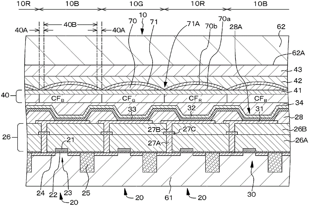
在包括上述优选形式的根据本公开的第一方面的发光元件等中,可以采用以下形式:位于中间层的外侧区域上的覆盖层的端部部分的层厚度T2大于0μm且为1.0μm或更小。在包括上述优选形式的根据本公开的第二方面的发光元件等中,可以采用以下的形式:位于密封树脂层的外侧区域上的覆盖层的端部部分的层厚度T2大于0μm且为0.5μm或更小。这里,覆盖层的端部部分的“层厚度T2”是指沿着与光路控制单元的光轴平行的虚拟直线从覆盖层的底部到顶部的距离。当层厚度取决于覆盖层的端部部分的位置而变化时,最小层厚度被定义为覆盖层的端部部分的层厚度。在本公开的显示设备等中,在构成相邻的发光元件的光路控制单元与光路控制单元之间存在间隙。仅需要将位于构成相邻的发光元件的光路控制单元和光路控制单元之间的覆盖层的最薄部分设置为覆盖层的端部部分。覆盖层可以具有单层结构或多层结构。In the light-emitting element or the like according to the first aspect of the present disclosure including the above-described preferred forms, a form in which the layer thickness T 2 of the end portion of the cover layer on the outer region of the intermediate layer is greater than 0 μm and 1.0 μm or smaller. In the light-emitting element or the like according to the second aspect of the present disclosure including the above-described preferred forms, a form in which the layer thickness T 2 of the end portion of the cover layer on the outer region of the sealing resin layer is greater than 0 μm and 0.5 μm may be employed. μm or less. Here, the "layer thickness T 2 " of the end portion of the cover layer refers to the distance from the bottom to the top of the cover layer along a virtual straight line parallel to the optical axis of the optical path control unit. When the layer thickness varies depending on the position of the end portion of the covering layer, the minimum layer thickness is defined as the layer thickness of the end portion of the covering layer. In the display device and the like of the present disclosure, there is a gap between the optical path control unit and the optical path control unit constituting adjacent light emitting elements. It is only necessary to set the thinnest portion of the cover layer between the light path control unit and the light path control unit constituting adjacent light emitting elements as the end portion of the cover layer. The covering layer may have a single-layer structure or a multi-layer structure.
此外,在包括上述优选形式的根据本公开的第一方面的发光元件等中,可以采用以下的形式:光路控制单元由具有凸形光出射表面的透镜构件构成。透镜构件的光入射表面例如是平坦的。在这种情况下,波长选择单元可以形成在中间层内部,并且此外,Furthermore, in the light emitting element or the like according to the first aspect of the present disclosure including the above preferred forms, a form may be adopted in which the optical path control unit is constituted by a lens member having a convex light exit surface. The light incident surface of the lens member is, for example, flat. In this case, the wavelength selective unit may be formed inside the intermediate layer, and furthermore,
覆盖层可以被树脂层覆盖,并且the cover layer may be covered by a resin layer, and
当构成树脂层的材料的平均折射率由n3表示时,When the average refractive index of the material constituting the resin layer is represented by n3 ,
可以满足n2>n3。可替换地,在这种形式下,n 2 >n 3 may be satisfied. Alternatively, in this form,
覆盖层可以被树脂层覆盖,The covering layer can be covered by a resin layer,
当构成树脂层的材料的平均折射率由n3表示时,When the average refractive index of the material constituting the resin layer is represented by n3 ,
可以满足n2>n3,并且can satisfy n 2 >n 3 , and
可以在树脂层内部或树脂层上形成波长选择单元。The wavelength selective unit may be formed inside or on the resin layer.
这里,here,
期望满足n2-n3>0.1。构成树脂层的材料的示例包括诸如丙烯酸粘合剂、环氧基粘合剂、聚氨酯基粘合剂、硅酮基粘合剂或氰基丙烯酸酯基粘合剂之类的热固性粘合剂和紫外线可固化粘合剂。用于形成树脂层的方法的示例包括真空注入法和液晶滴注法。It is desirable to satisfy n 2 -n 3 >0.1. Examples of materials constituting the resin layer include thermosetting adhesives such as acrylic adhesives, epoxy-based adhesives, urethane-based adhesives, silicone-based adhesives, or cyanoacrylate-based adhesives, and UV curable adhesive. Examples of methods for forming the resin layer include a vacuum injection method and a liquid crystal dropping method.
在根据本公开的第一方面的发光元件等中,当覆盖层由多个层构成时,优选的是从光入射侧朝向光出射侧,使构成覆盖层的材料的折射率的值减小。In the light emitting element or the like according to the first aspect of the present disclosure, when the cover layer is composed of a plurality of layers, it is preferable to decrease the value of the refractive index of the material constituting the cover layer from the light incident side toward the light exit side.
在包括上述优选形式的根据本公开的第二方面的发光元件等中,可以采用以下的形式:光路控制单元由具有凸形光入射表面的透镜构件构成。透镜构件的光出射表面例如是平坦的。在这种情况下,波长选择单元可以形成在密封树脂层内部。可替换地,波长选择单元可以形成在平坦化膜和光路控制单元之间,或者波长选择单元可以形成在平坦化膜和第二基板之间。可替换地,保护层可以形成在密封树脂层和发光单元之间,并且此外,波长选择单元可以形成在保护层内部或保护层上。此外,在这些形式和构造中,当构成密封树脂层的材料的平均折射率由n3表示时,In the light emitting element or the like according to the second aspect of the present disclosure including the above preferred forms, a form may be adopted in which the optical path control unit is constituted by a lens member having a convex light incident surface. The light exit surface of the lens member is, for example, flat. In this case, the wavelength selection unit may be formed inside the sealing resin layer. Alternatively, the wavelength selection unit may be formed between the planarization film and the optical path control unit, or the wavelength selection unit may be formed between the planarization film and the second substrate. Alternatively, a protective layer may be formed between the sealing resin layer and the light emitting unit, and further, the wavelength selection unit may be formed inside or on the protective layer. Furthermore, in these forms and configurations, when the average refractive index of the material constituting the sealing resin layer is represented by n 3 ,
可以满足n2>n3。n 2 >n 3 may be satisfied.
这里,期望满足n2-n3>0.1。构成密封树脂层的材料的示例包括诸如丙烯酸类粘合剂、环氧基粘合剂、聚氨酯基粘合剂、硅酮基粘合剂或氰基丙烯酸酯基粘合剂之类的热固性粘合剂和紫外线可固化粘合剂。用于形成密封树脂层的方法的示例包括真空注入法和液晶滴注法。Here, it is desirable to satisfy n 2 -n 3 >0.1. Examples of materials constituting the sealing resin layer include thermosetting adhesives such as acrylic adhesives, epoxy-based adhesives, urethane-based adhesives, silicone-based adhesives, or cyanoacrylate-based adhesives. adhesives and UV curable adhesives. Examples of methods for forming the sealing resin layer include a vacuum injection method and a liquid crystal dropping method.
在根据本公开的第二方面的发光元件等中,当覆盖层由多个层构成时,优选的是从光入射侧朝向光出射侧,使构成覆盖层的材料的折射率值增大。In the light emitting element or the like according to the second aspect of the present disclosure, when the cover layer is composed of a plurality of layers, it is preferable to increase the refractive index value of the material constituting the cover layer from the light incident side toward the light exit side.
在包括上述各种优选形式和构造的本公开的发光元件等中,当光路控制单元由凸透镜构件(芯片上微凸透镜)构成时,构成光路控制单元和覆盖层的材料的示例包括以下材料,但不限于此。In the light-emitting element and the like of the present disclosure including the various preferred forms and configurations described above, when the optical path control unit is composed of a convex lens member (on-chip lenticular lens), examples of materials constituting the optical path control unit and the cover layer include the following materials, but Not limited to this.
[光路控制单元][Optical path control unit]
丙烯酸透明树脂(折射率:1.54)Acrylic transparent resin (refractive index: 1.54)
环氧基透明树脂(折射率:1.55)Epoxy transparent resin (refractive index: 1.55)
TiO2分散的丙烯酸透明树脂(折射率:1.72)TiO 2 dispersed acrylic transparent resin (refractive index: 1.72)
SiN(折射率:1.74)SiN (refractive index: 1.74)
[覆盖层][overlay]
中空含二氧化硅氟基低折射率透明树脂(折射率:1.25)Hollow silica-containing fluorine-based low-refractive index transparent resin (refractive index: 1.25)
氟基低折射率透明树脂(折射率:1.38)Fluorine-based low refractive index transparent resin (refractive index: 1.38)
丙烯酸透明树脂(折射率:1.54)Acrylic transparent resin (refractive index: 1.54)
环氧基透明树脂(折射率:1.55)Epoxy transparent resin (refractive index: 1.55)
Al2O3分散的丙烯酸透明树脂(折射率:1.64)Al 2 O 3 dispersed acrylic transparent resin (refractive index: 1.64)
具体地,[构成光路控制单元的材料和构成覆盖层的材料]的组合的示例包括但不限于,Specifically, examples of combinations of [the material constituting the optical path control unit and the material constituting the covering layer] include, but are not limited to,
[丙烯酸透明树脂和中空含二氧化硅氟基低折射率透明树脂],[Acrylic transparent resin and hollow silica-containing fluorine-based low-refractive index transparent resin],
[丙烯酸透明树脂和氟基低折射率透明树脂],[Acrylic transparent resin and fluorine-based low refractive index transparent resin],
[环氧基透明树脂和中空含二氧化硅氟基低折射率透明树脂],[Epoxy-based transparent resin and hollow silica-containing fluorine-based low-refractive index transparent resin],
[环氧基透明树脂和氟基低折射率透明树脂],[Epoxy-based transparent resin and fluorine-based low-refractive-index transparent resin],
[TiO2分散的丙烯酸透明树脂和氟基低折射率透明树脂],[ TiO2 dispersed acrylic transparent resin and fluorine-based low refractive index transparent resin],
[TiO2分散的丙烯酸透明树脂和丙烯酸透明树脂],[TiO 2 dispersed acrylic transparent resin and acrylic transparent resin],
[SiN无机膜和氟基低折射率透明树脂],以及[SiN inorganic film and fluorine-based low-refractive-index transparent resin], and
[SiN无机膜和丙烯酸透明树脂]。[SiN inorganic film and acrylic transparent resin].
构成中间层和平坦化膜的材料的示例包括丙烯酸树脂、环氧基树脂和各种无机材料(例如,SiO2、SiN、SiON、SiC、非晶硅(α-Si)、Al2O3和TiO2)。中间层和平坦化膜可以各自具有单层结构或多层结构。在后一种情况下,在根据本公开的第一方面的发光元件等中,优选的是从光入射方向朝向光出射方向,顺次地减小构成中间层的材料的折射率的值。在根据本公开的第二方面的发光元件等中,优选的是从光入射方向朝向光出射方向,顺次地增大构成平坦化膜的材料的折射率的值。可以基于诸如各种CVD方法、各种涂覆方法、包括溅射方法和真空蒸发沉积方法的各种PVD方法以及诸如丝网印刷方法之类的各种印刷方法之类的已知方法来形成中间层和平坦化膜。中间层和平坦化膜中的每一个可以由多个发光元件共享,或者可以单独地形成在发光元件中的每一个上。Examples of materials constituting the intermediate layer and the planarizing film include acrylic resins, epoxy-based resins, and various inorganic materials (for example, SiO 2 , SiN, SiON, SiC, amorphous silicon (α-Si), Al 2 O 3 , and TiO 2 ). The intermediate layer and the planarizing film may each have a single-layer structure or a multi-layer structure. In the latter case, in the light emitting element or the like according to the first aspect of the present disclosure, it is preferable to sequentially decrease the value of the refractive index of the material constituting the intermediate layer from the light incident direction toward the light exit direction. In the light-emitting element or the like according to the second aspect of the present disclosure, it is preferable to sequentially increase the value of the refractive index of the material constituting the planarizing film from the light incident direction toward the light exit direction. The intermediate can be formed based on known methods such as various CVD methods, various coating methods, various PVD methods including sputtering methods and vacuum evaporation deposition methods, and various printing methods such as screen printing methods. layer and planarization film. Each of the intermediate layer and the planarizing film may be shared by a plurality of light emitting elements, or may be individually formed on each of the light emitting elements.
在包括上述各种优选形式和构造的本公开的发光元件等中,可以采用发光单元包括有机电致发光层的形式。即,可以采用包括上述各种优选形式和构造的本公开的发光元件等由有机电致发光元件(有机EL元件)构成的形式,并且可以采用本公开的显示设备等由有机电致发光显示设备(有机EL显示设备)构成的形式。In the light-emitting element and the like of the present disclosure including the various preferred forms and configurations described above, a form in which the light-emitting unit includes an organic electroluminescent layer may be employed. That is, a form in which the light-emitting element of the present disclosure, etc., including the above-mentioned various preferred forms and configurations, is composed of an organic electroluminescent element (organic EL element) can be adopted, and a display device of the present disclosure, etc., composed of an organic electroluminescence display device can be adopted. (Organic EL display device) form.
这里,换句话说,本公开的显示设备等包括:Here, in other words, the display device and the like of the present disclosure include:
第一基板和第二基板;以及a first substrate and a second substrate; and
多个发光元件,所述多个发光元件位于第一基板和第二基板之间并被二维地布置,其中,a plurality of light emitting elements positioned between the first substrate and the second substrate and arranged two-dimensionally, wherein,
发光元件中的每一个由包括上述优选形式的本公开的发光元件等构成,并且Each of the light-emitting elements is constituted by the light-emitting element of the present disclosure including the above-mentioned preferred forms, and the like, and
来自发光单元的光经由第二基板发射到外部。即,本公开的显示设备等可以是从第二基板发射光的顶部发射型显示设备。Light from the light emitting unit is emitted to the outside through the second substrate. That is, the display device or the like of the present disclosure may be a top emission type display device that emits light from the second substrate.
在本公开的显示设备等中,像素(或子像素)的布置的示例包括三角形布置、条形布置、对角布置、矩形布置、四边形布置和方形布置。根据像素(或子像素)的布置,波长选择单元的布置也只需要是三角形布置、条形布置、对角布置、矩形布置、四边形布置或方形布置。In the display device and the like of the present disclosure, examples of the arrangement of pixels (or sub-pixels) include a triangular arrangement, a stripe arrangement, a diagonal arrangement, a rectangular arrangement, a quadrangular arrangement, and a square arrangement. According to the arrangement of pixels (or sub-pixels), the arrangement of the wavelength selective units only needs to be a triangular arrangement, a strip arrangement, a diagonal arrangement, a rectangular arrangement, a quadrangular arrangement or a square arrangement.
在包括上述各种优选形式和构造的本公开的发光元件等中,可以采用光路控制单元被形成为半球形形状或由球体的一部分形成的形状的形式,或者广义上可以采用光路控制单元被形成为适于用作透镜的形状的形式。具体地,如上所述,光路控制单元可以由凸透镜构件(具体地,平凸透镜)构成。可替换地,透镜构件可以是球面透镜或非球面透镜。光路控制单元可以是折射透镜或衍射透镜。In the light-emitting element and the like of the present disclosure including the various preferred forms and configurations described above, a form in which the optical path control unit is formed in a hemispherical shape or a shape formed by a part of a sphere, or in a broad sense may be adopted in which the optical path control unit is formed It is a shape suitable for use as a lens. Specifically, as described above, the optical path control unit may be constituted by a convex lens member (specifically, a plano-convex lens). Alternatively, the lens member may be a spherical lens or an aspherical lens. The optical path control unit may be a refractive lens or a diffractive lens.
可替换地,假定具有方形或矩形底表面的长方体,并且也可以采用以下的三维形状的透镜构件:长方体的四个侧表面和一个顶表面各自具有凸形状,侧表面彼此相交的棱的部分被圆形化,顶表面与侧表面相交的棱的部分也被圆形化,并且透镜构件作为整体被圆形化。可替换地,假定具有方形或矩形底表面的长方体(包括近似长方体的立方体),并且可以采用长方体的四个侧表面和一个顶表面是平面的透镜构件。在这种情况下,在某些情况下,可以采用侧表面彼此相交的棱的部分被圆形化的三维形状的透镜构件,并且在某些情况下,也可以采用顶表面与侧表面相交的棱的部分也被圆形化的三维形状的透镜构件。可替换地,可以采用透镜构件由当沿着包括厚度方向的虚拟平面(垂直虚拟平面)切割时具有矩形或等腰梯形截面形状的透镜构件构成的形式。换句话说,可以采用透镜构件由截面形状在其厚度方向上恒定或变化的透镜构件构成的形式。Alternatively, assume a cuboid having a square or rectangular bottom surface, and a lens member of a three-dimensional shape in which each of the four side surfaces and one top surface of the cuboid has a convex shape, and the portion of the edge where the side surfaces meet each other is With circularization, the portion of the rib where the top surface intersects the side surface is also circularized, and the lens member as a whole is circularized. Alternatively, a cuboid (including a cube approximately cuboid) having a square or rectangular bottom surface is assumed, and a lens member whose four side surfaces and one top surface of the cuboid are flat may be employed. In this case, in some cases, a lens member of a three-dimensional shape in which the portion of the rib where the side surfaces meet each other is rounded may be used, and in some cases, a lens member in which the top surface and the side surface meet may also be used. A three-dimensional lens member in which the ribs are also rounded. Alternatively, a form may be employed in which the lens member is composed of a lens member having a rectangular or isosceles trapezoidal sectional shape when cut along an imaginary plane (perpendicular imaginary plane) including the thickness direction. In other words, a form may be employed in which the lens member is composed of a lens member whose cross-sectional shape is constant or varies in its thickness direction.
可替换地,在根据本公开的第一方面的发光元件等中,可以采用光路控制单元由当沿着包括其厚度方向的虚拟平面(垂直虚拟平面)切割时具有矩形或等腰梯形截面形状的光出射方向控制构件构成的形式。换句话说,可以采用光路控制单元由截面形状在其厚度方向上恒定或变化的光出射方向控制构件构成的形式。将在示例3中详细地描述光出射方向控制构件。Alternatively, in the light-emitting element or the like according to the first aspect of the present disclosure, the optical path control unit may be formed of a rectangular or isosceles trapezoidal cross-sectional shape when cut along a virtual plane (perpendicular virtual plane) including its thickness direction. The form of the configuration of the light emission direction control member. In other words, a form may be employed in which the optical path control unit is constituted by a light exit direction control member whose cross-sectional shape is constant or variable in its thickness direction. The light exit direction control member will be described in detail in Example 3.
在包括上述各种优选形式和构造的本公开的发光元件等中,当为了方便起见将光路控制单元沿着光轴的厚度(沿着光轴的光路控制单元的两个面对的透镜表面之间的距离)被称为“光路控制单元的高度”时,可以采用光路控制单元的高度H0和构成相邻的发光元件的光路控制单元之间的最小距离(间隙)2L0满足0<2L0/H0≤0.5的形式。当发光元件的尺寸(像素或子像素一侧的长度)为1.00时,最小距离(间隙)2L0优选地为0.1或更小,并且相邻的光路控制单元的光轴之间的距离优选地为1μm或更大且10μm或更小。In the light-emitting element of the present disclosure including the various preferred forms and configurations described above, when the thickness of the optical path control unit along the optical axis (between the two facing lens surfaces of the optical path control unit along the optical axis When the distance between them) is referred to as the "height of the optical path control unit", the height H of the optical path control unit and the minimum distance (gap) 2L 0 between the optical path control units constituting adjacent light-emitting elements can be used to satisfy 0<2L 0 /H 0 ≤ 0.5 form. When the size of the light-emitting element (the length of one side of a pixel or sub-pixel) is 1.00, the minimum distance (gap) 2L 0 is preferably 0.1 or less, and the distance between the optical axes of adjacent optical path control units is preferably 1 μm or more and 10 μm or less.
另外,在根据本公开的第一方面的发光元件等中,位于密封树脂层的外侧区域上的覆盖层的端部部分的层厚度T2与最小距离(间隙)2L0之间的关系的示例包括但不限于,In addition, in the light emitting element or the like according to the first aspect of the present disclosure, an example of the relationship between the layer thickness T 2 of the end portion of the cover layer positioned on the outer region of the sealing resin layer and the minimum distance (gap) 2L 0 including but not limited to,
0≤T2/L0≤2.5。0 ≤ T 2 /L 0 ≤ 2.5.
光路控制单元的平面形状的尺寸可以取决于发光元件而改变。例如,当一个像素由三个子像素构成时,光路控制单元的平面形状的尺寸在构成一个像素的三个子像素中可以是相同值、在除了一个子像素之外的两个子像素中可以是相同值、或者在三个子像素中可以是不同值。另外,构成光路控制单元的材料的折射率可以取决于发光元件而改变。例如,当一个像素由三个子像素构成时,构成光路控制单元的材料的折射率在构成一个像素的三个子像素中可以是相同值、在除了一个子像素之外的两个子像素中可以是相同值、或者在三个子像素中可以是不同值。The size of the planar shape of the optical path control unit may vary depending on the light emitting element. For example, when one pixel is composed of three sub-pixels, the size of the planar shape of the optical path control unit may be the same value in three sub-pixels constituting one pixel, and may be the same value in two sub-pixels except for one sub-pixel. , or may be different values in the three sub-pixels. In addition, the refractive index of the material constituting the optical path control unit may vary depending on the light emitting element. For example, when one pixel is composed of three sub-pixels, the refractive index of the material constituting the optical path control unit may be the same value in three sub-pixels constituting one pixel, and may be the same in two sub-pixels except for one sub-pixel. value, or may be different values among the three sub-pixels.
当一个像素由多个子像素构成时,可以对应于一个子像素部署一个透镜构件,或者可以对应于一个子像素部署多个透镜构件。When one pixel is composed of a plurality of sub-pixels, one lens member may be disposed corresponding to one sub-pixel, or a plurality of lens members may be disposed corresponding to one sub-pixel.
透镜构件可以通过使构成透镜构件的透明树脂材料熔融流动或回蚀构成透镜构件的透明树脂材料来获得、可以通过基于有机材料或无机材料使用灰色调掩模或半色调掩模的光刻技术与刻蚀方法的组合来获得、或者可以通过用于基于纳米压印方法将透明树脂材料形成为透镜形状的方法来获得。构成透镜构件(微透镜)的材料的示例包括如上所述的高折射率树脂材料和高折射率无机膜(用于凸透镜)。The lens member can be obtained by melt-flowing or etching back the transparent resin material constituting the lens member, and can be obtained by photolithography using a gray-tone mask or a half-tone mask based on an organic material or an inorganic material. It may be obtained by a combination of etching methods, or may be obtained by a method for forming a transparent resin material into a lens shape based on a nanoimprint method. Examples of materials constituting the lens member (microlens) include high-refractive-index resin materials and high-refractive-index inorganic films (for convex lenses) as described above.
用于形成覆盖层的方法的示例包括旋涂法、喷涂法、淋涂法、各种辊涂法和浸涂法。当基于涂覆方法来形成覆盖层时,优选的是选择具有低粘度和良好润湿性的材料。可替换地,可以通过采用各种CVD方法[例如,通过高密度等离子体化学气相沉积方法(HDP-CVD方法)或表面反应执行膜形成的CVD方法(共形(conformal)CVD方法)]或原子层沉积法(ALD方法)作为用于形成覆盖层的方法来获得共形覆盖层。可替换地,覆盖层可以通过使构成覆盖层的透明树脂材料熔融流动或回蚀构成覆盖层的透明树脂材料来获得、或者可以通过基于有机材料或无机材料使用灰色调掩模或半色调掩模的光刻技术与刻蚀方法的组合来获得。Examples of methods for forming the covering layer include spin coating, spray coating, flow coating, various roll coating methods, and dip coating methods. When forming the covering layer based on a coating method, it is preferable to select a material having low viscosity and good wettability. Alternatively, various CVD methods [for example, a CVD method (conformal CVD method) that performs film formation by a high-density plasma chemical vapor deposition method (HDP-CVD method) or a surface reaction]] or atomic A layer deposition method (ALD method) is used as a method for forming the covering layer to obtain a conformal covering layer. Alternatively, the cover layer may be obtained by melt-flowing or etching back a transparent resin material constituting the cover layer, or may be obtained by using a gray-tone mask or a half-tone mask based on an organic material or an inorganic material The combination of photolithography and etching methods is obtained.
如上所述,可以采用从发光单元发射的光依次经过波长选择单元和光路控制单元的形式,或者可以采用从发光单元发射的光依次经过光路控制单元和波长选择单元的形式。当正交投影图像是第一基板上的正交投影图像时,可以采用光路控制单元的正交投影图像与波长选择单元的正交投影图像重合的形式,可以采用光路控制单元的正交投影图像被包括在波长选择单元的正交投影图像中的形式,或者可以采用波长选择单元的正交投影图像被包括在光路控制单元的正交投影图像中的形式。通过采用光路控制单元的正交投影图像被包括在波长选择单元的正交投影图像中的形式,可以可靠地抑制相邻的发光元件之间的颜色混合的发生。As described above, the light emitted from the light-emitting unit may pass through the wavelength selection unit and the optical path control unit in sequence, or the light emitted from the light-emitting unit may pass through the optical path control unit and the wavelength selection unit in sequence. When the orthogonal projection image is an orthogonal projection image on the first substrate, the orthogonal projection image of the optical path control unit and the orthogonal projection image of the wavelength selection unit can be overlapped, and the orthogonal projection image of the optical path control unit can be used The form included in the orthogonal projection image of the wavelength selection unit, or the form in which the orthogonal projection image of the wavelength selection unit is included in the orthogonal projection image of the optical path control unit may be adopted. By adopting a form in which the orthogonal projection image of the optical path control unit is included in the orthogonal projection image of the wavelength selection unit, occurrence of color mixture between adjacent light emitting elements can be reliably suppressed.
可替换地,波长选择单元的平面形状可以与光路控制单元的平面形状相同、相似、近似或不同。另外,波长选择单元的平面形状可以与发光区域的平面形状相同、相似、近似或不同,但波长选择单元优选地大于发光区域。波长选择单元(例如,滤色器层)的尺寸可以取决于从发光元件发射的光而适当地改变。另外,波长选择单元(例如,滤色器层)的尺寸可以取决于经过发光区域的中心的法线与经过波长选择单元的中心的法线之间的距离(偏移量)d0(稍后描述)来适当地改变。Alternatively, the planar shape of the wavelength selection unit may be the same as, similar to, similar to, or different from that of the optical path control unit. In addition, the planar shape of the wavelength selective unit may be the same, similar, similar or different from that of the light emitting region, but the wavelength selective unit is preferably larger than the light emitting region. The size of the wavelength selection unit (eg, color filter layer) may be appropriately changed depending on light emitted from the light emitting element. In addition, the size of the wavelength selective unit (e.g., color filter layer) may depend on the distance (offset) d 0 (later description) to change appropriately.
波长选择单元可以由例如滤色器层构成。滤色器层由添加了包括期望的颜料或染料的着色剂的树脂制成,并且通过选择颜料或染料,滤色器层被调整以使得在诸如红色、绿色或蓝色之类的目标波长区域中的光透射率高,而其它波长区域中的光透射率低。可替换地,波长选择单元也可以由应用了光子晶体或等离子体激元的波长选择元件(具有在导体薄膜中形成格子状空穴结构的导体晶格结构的滤色器层,例如参见JP2008-177191A)、由诸如非晶硅之类的无机材料制成的薄膜、或量子点构成。下文中,滤色器层可以被描述为波长选择单元的代表,但波长选择单元不限于滤色器层。The wavelength selective unit may consist of, for example, a color filter layer. The color filter layer is made of a resin to which a colorant including a desired pigment or dye is added, and by selecting the pigment or dye, the color filter layer is adjusted so that in a target wavelength region such as red, green, or blue The light transmittance is high in , while the light transmittance in other wavelength regions is low. Alternatively, the wavelength selection unit can also be composed of a wavelength selection element using a photonic crystal or a plasmon (a color filter layer having a conductor lattice structure in which a grid-like hole structure is formed in a conductor film, see for example JP2008- 177191A), thin films of inorganic materials such as amorphous silicon, or quantum dots. Hereinafter, the color filter layer may be described as a representative of the wavelength selection unit, but the wavelength selection unit is not limited to the color filter layer.
此外,如上所述,在包括上述优选形式和构造的本公开的显示设备等中,可以采用在波长选择单元和波长选择单元之间或者在波长选择单元和波长选择单元之间的空间上方形成光吸收层(黑矩阵层)的形式,由此可以可靠地抑制相邻的发光元件之间的颜色混合的发生。光吸收层(黑矩阵层)由例如混合有黑色着色剂并具有1或更大的光浓度的黑色树脂膜(具体地,例如,黑色聚酰亚胺类树脂)构成,或者由使用薄膜的干涉的薄膜滤光器构成。薄膜滤光器通过例如层叠由金属、金属氮化物或金属氧化物制成的两个或更多个薄膜来形成,并使用薄膜的干涉来衰减光。薄膜滤光器的具体示例包括Cr和铬(III)氧化物(Cr2O3)交替层叠的薄膜滤光器。可以取决于从发光元件发射的光来适当地改变光吸收层(黑矩阵层)的尺寸。In addition, as described above, in the display device or the like of the present disclosure including the above-described preferred forms and configurations, it is possible to adopt the method of forming light between the wavelength selection unit and the wavelength selection unit or above the space between the wavelength selection unit and the wavelength selection unit. In the form of an absorbing layer (black matrix layer), the occurrence of color mixing between adjacent light emitting elements can thus be reliably suppressed. The light absorbing layer (black matrix layer) is made of, for example, a black resin film (specifically, for example, black polyimide-based resin) mixed with a black colorant and has a light density of 1 or more, or is made of an interference film using a thin film. of thin film filters. A thin film filter is formed by, for example, laminating two or more thin films made of metal, metal nitride, or metal oxide, and attenuates light using interference of the thin films. Specific examples of the thin film filter include a thin film filter in which Cr and chromium (III) oxide (Cr 2 O 3 ) are alternately laminated. The size of the light absorbing layer (black matrix layer) can be appropriately changed depending on the light emitted from the light emitting element.
下文中,关注于发光单元,将描述构成发光元件的发光单元包括有机电致发光层的形式,即,本公开的显示设备等由有机电致发光显示设备(有机EL显示设备)构成的形式。Hereinafter, focusing on the light-emitting unit, a form in which the light-emitting unit constituting the light-emitting element includes an organic electroluminescent layer, that is, a form in which the display device of the present disclosure is composed of an organic electroluminescent display device (organic EL display device) will be described.
一种有机EL显示设备,包括:An organic EL display device, comprising:
第一基板和第二基板;以及a first substrate and a second substrate; and
多个发光元件,所述多个发光元件位于第一基板和第二基板之间并被二维地布置,其中,a plurality of light emitting elements positioned between the first substrate and the second substrate and arranged two-dimensionally, wherein,
部署在形成在第一基板上的基底上的发光元件中的每一个包括发光单元,each of the light emitting elements disposed on the base formed on the first substrate includes a light emitting unit,
发光单元至少包括:The lighting unit includes at least:
第一电极;first electrode;
第二电极;以及the second electrode; and
有机层(包括由有机电致发光层构成的发光层),所述有机层夹在第一电极和第二电极之间,以及an organic layer (including a light-emitting layer composed of an organic electroluminescent layer), the organic layer being sandwiched between the first electrode and the second electrode, and
来自有机层的光经由第二基板发射到外部。Light from the organic layer is emitted to the outside through the second substrate.
第一电极针对发光元件中的每一个部署。有机层针对发光元件中的每一个部署,或者被部署为由发光元件共享。第二电极可以是由多个发光元件共享的电极。即,第二电极可以是所谓的固体电极。第一基板部署在基底的下面或下方,并且第二基板部署在第二电极上方。发光元件形成在第一基板侧,并且发光单元部署在基底上。A first electrode is disposed for each of the light emitting elements. An organic layer is disposed for each of the light emitting elements, or is disposed to be shared by the light emitting elements. The second electrode may be an electrode shared by a plurality of light emitting elements. That is, the second electrode may be a so-called solid electrode. The first substrate is disposed under or below the base, and the second substrate is disposed above the second electrode. The light emitting element is formed on the first substrate side, and the light emitting unit is disposed on the base.
第一电极可以与有机层的一部分接触,或者有机层可以与第一电极的一部分接触。具体地,第一电极的尺寸可以小于有机层的尺寸。可替换地,第一电极的尺寸可以与有机层的尺寸相同,但绝缘层可以形成在第一电极和有机层之间的空间的一部分中。可替换地,第一电极的尺寸可以大于有机层的尺寸。发光区域的尺寸是第一电极与有机层彼此接触的区域的尺寸。发光区域的尺寸可以取决于从发光元件发射的光的颜色而改变。The first electrode may be in contact with a part of the organic layer, or the organic layer may be in contact with a part of the first electrode. Specifically, the size of the first electrode may be smaller than that of the organic layer. Alternatively, the size of the first electrode may be the same as that of the organic layer, but the insulating layer may be formed in a part of the space between the first electrode and the organic layer. Alternatively, the size of the first electrode may be larger than that of the organic layer. The size of the light emitting region is the size of a region where the first electrode and the organic layer are in contact with each other. The size of the light emitting area may vary depending on the color of light emitted from the light emitting element.
可以采用有机层发射白光的形式,并且在这种情况下,可以采用有机层由发射不同颜色的至少两个发光层构成的形式。具体地,可以采用以下的形式:有机层具有发射红光(波长:620nm至750nm)的红色发光层、发射绿光(波长:495nm至570nm)的绿色发光层以及发射蓝光(波长:450nm至495nm)的蓝色发光层被层叠的层叠结构,并作为整体发射白光。可替换地,有机层可以具有发射蓝光的蓝色发光层和发射黄光的黄色发光层的两个层被层叠的结构并作为整体发射白光。可替换地,有机层可以具有发射蓝光的蓝色发光层和发射橙色光的橙色发光层的两个层被层叠的结构并作为整体发射白光。有机层可以由多个发光元件共享,或者可以单独地形成在发光元件中的每一个中。这样的发射白光的有机层(发光单元)和红色滤色器层(或用作红色滤色器层的中间层)被组合,以构成红色发光元件,发射白光的有机层(发光单元)和绿色滤色器层(或用作绿色滤色器层的中间层)被组合,以构成绿色发光元件,并且发射白光的有机层(发光单元)和蓝色滤色器层(或用作蓝色滤色器层的中间层)被组合以构成蓝色发光元件。诸如红色发光元件、绿色发光元件和蓝色发光元件之类的子像素的组合构成发光元件单元(一个像素)。在某些情况下,红色发光元件、绿色发光元件、蓝色发光元件和发射白色(或第四种颜色)光的发光元件(或发射互补颜色光的发光元件)可以构成发光元件单元(一个像素)。在由发射不同颜色的至少两个发光层构成的形式中,实际上,发射不同颜色的发光层被彼此混合,并且在某些情况下,没有被清楚地分离成层。A form in which the organic layer emits white light may be employed, and in this case, a form in which the organic layer is composed of at least two light emitting layers emitting different colors may be employed. Specifically, the following form can be adopted: the organic layer has a red light emitting layer emitting red light (wavelength: 620nm to 750nm), a green light emitting layer emitting green light (wavelength: 495nm to 570nm), and a blue light emitting layer (wavelength: 450nm to 495nm). ) in which the blue light-emitting layers are laminated, and emit white light as a whole. Alternatively, the organic layer may have a structure in which two layers of a blue light emitting layer emitting blue light and a yellow light emitting layer emitting yellow light are laminated and emit white light as a whole. Alternatively, the organic layer may have a structure in which two layers of a blue light emitting layer emitting blue light and an orange light emitting layer emitting orange light are laminated and emit white light as a whole. The organic layer may be shared by a plurality of light emitting elements, or may be separately formed in each of the light emitting elements. Such an organic layer (light-emitting unit) emitting white light and a red color filter layer (or an intermediate layer serving as a red color filter layer) are combined to constitute a red light-emitting element, an organic layer (light-emitting unit) emitting white light and a green color filter layer. A color filter layer (or an intermediate layer used as a green color filter layer) is combined to constitute a green light-emitting element, and an organic layer (light-emitting unit) emitting white light and a blue color filter layer (or used as a blue filter layer) The middle layer of the color shader layer) is combined to form a blue light-emitting element. A combination of sub-pixels such as a red light-emitting element, a green light-emitting element, and a blue light-emitting element constitutes a light-emitting element unit (one pixel). In some cases, a red light-emitting element, a green light-emitting element, a blue light-emitting element, and a light-emitting element emitting white (or fourth color) light (or a light-emitting element emitting complementary color light) may constitute a light-emitting element unit (one pixel ). In a form consisting of at least two light-emitting layers emitting different colors, in fact, the light-emitting layers emitting different colors are mixed with each other and, in some cases, are not clearly separated into layers.
如上所述,具有滤色器层功能的中间层仅需要由已知的耐色材料制成。在发射白光的发光元件中,只需要部署透明滤光层。当如上所述中间层也用作滤色器层时,有机层与中间层(滤色器层)彼此接近。因此,即使从发光元件发射的光的角度变宽,也可以有效地防止颜色混合,并且视角特性被改善。As described above, the intermediate layer having the function of the color filter layer only needs to be made of known color-resistant materials. In light-emitting elements that emit white light, only a transparent filter layer needs to be deployed. When the intermediate layer is also used as the color filter layer as described above, the organic layer and the intermediate layer (color filter layer) are close to each other. Therefore, even if the angle of light emitted from the light emitting element is widened, color mixture can be effectively prevented, and viewing angle characteristics are improved.
可替换地,可以采用有机层由一个发光层构成的形式。在这种情况下,发光元件可以由例如具有包括红色发光层的有机层的红色发光元件、具有包括绿色发光层的有机层的绿色发光元件或具有包括蓝色发光层的有机层的蓝色发光元件构成。在彩色显示设备的情况下,一个像素由这三种类型的发光元件(子像素)构成。注意的是,原则上,不需要形成滤色器层,但为了提高颜色纯度,可以形成滤色器层。可替换地,发光元件可以由具有包括红光发光层的有机层的红色发光元件、具有包括绿光发光层的有机层的绿色发光元件和具有包括蓝光发光层的有机层的蓝色发光元件的层叠结构(发光元件的层叠结构)构成。Alternatively, a form in which the organic layer is composed of one light emitting layer may be employed. In this case, the light-emitting element can be made of, for example, a red light-emitting element having an organic layer including a red light-emitting layer, a green light-emitting element having an organic layer including a green light-emitting layer, or a blue light-emitting element having an organic layer including a blue light-emitting layer. Component composition. In the case of a color display device, one pixel is composed of these three types of light emitting elements (sub-pixels). Note that, in principle, it is not necessary to form a color filter layer, but in order to improve color purity, a color filter layer may be formed. Alternatively, the light emitting element may be composed of a red light emitting element having an organic layer including a red light emitting layer, a green light emitting element having an organic layer including a green light emitting layer, and a blue light emitting element having an organic layer including a blue light emitting layer Laminated structure (laminated structure of light-emitting elements) configuration.
当发光元件单元(一个像素)由多个发光元件(子像素)构成时,发光元件的发光区域的尺寸可以根据发光元件而改变。具体地,可以采用蓝色发光元件的发光区域的尺寸大于红色发光元件的发光区域的尺寸和绿色发光元件的发光区域的尺寸的形式。结果,可以使蓝色发光元件的光发射量大于红光发光元件的光发射量和绿色发光元件的光发射量。可替换地,可以使蓝色发光元件的光发射量、红色发光元件的光发射量和绿色发光元件的光发射量适当,并且图像质量可以提高。可替换地,当假定由除了红色发光元件、绿色发光元件和蓝色发光元件之外的发射白光的白色发光元件构成的发光元件单元(一个像素)时,从亮度的观点来看,绿色发光元件或白色发光元件的发光区域的尺寸优选地大于红色发光元件或蓝色发光元件的发光区域的尺寸。另外,从发光元件的寿命的观点来看,蓝色发光元件的发光区域的尺寸优选地大于红色发光元件、绿色发光元件或白色发光元件的发光区域的尺寸。注意的是,本公开不限于这些。When a light emitting element unit (one pixel) is constituted by a plurality of light emitting elements (subpixels), the size of the light emitting area of the light emitting element may vary depending on the light emitting element. Specifically, a form in which the size of the light-emitting region of the blue light-emitting element is larger than the size of the light-emitting region of the red light-emitting element and the size of the light-emitting region of the green light-emitting element may be adopted. As a result, the light emission amount of the blue light emitting element can be made larger than that of the red light emitting element and that of the green light emitting element. Alternatively, the light emission amount of the blue light emitting element, the light emission amount of the red light emitting element, and the light emission amount of the green light emitting element can be made appropriate, and the image quality can be improved. Alternatively, when a light-emitting element unit (one pixel) constituted by a white light-emitting element emitting white light other than a red light-emitting element, a green light-emitting element, and a blue light-emitting element is assumed, from the viewpoint of brightness, the green light-emitting element Or the size of the light emitting area of the white light emitting element is preferably larger than the size of the light emitting area of the red light emitting element or the blue light emitting element. In addition, from the viewpoint of the lifetime of the light emitting element, the size of the light emitting region of the blue light emitting element is preferably larger than the size of the light emitting region of the red light emitting element, the green light emitting element, or the white light emitting element. Note that the present disclosure is not limited to these.
有机层包括含有有机发光材料的发光层。具体地,有机层可以由例如空穴传输层、发光层和电子传输层的层叠结构、空穴传输层和也用作电子传输层的发光层的层叠结构、或者空穴注入层、空穴传输层、发光层、电子传输层和电子注入层的层叠结构构成。The organic layer includes a light emitting layer containing an organic light emitting material. Specifically, the organic layer can be composed of, for example, a hole transport layer, a stacked structure of a light-emitting layer and an electron transport layer, a stacked structure of a hole transport layer and a light-emitting layer also serving as an electron transport layer, or a hole injection layer, a hole transport layer, or a hole transport layer. Layer, light-emitting layer, electron transport layer and electron injection layer of the laminated structure.
用于形成有机层的方法的示例包括:诸如真空气相沉积方法之类的物理气相沉积方法(PVD方法);诸如丝网印刷方法或喷墨印刷方法之类的印刷方法;用激光照射形成在转印基板上的激光吸收层和有机层的层叠结构,以分离激光吸收层上的有机层并转印有机层的激光转印方法;以及各种涂覆方法。当基于真空气相沉积方法形成有机层时,例如,使用所谓的金属掩模,并且已经过形成在金属掩模中的开口的材料被沉积以获得有机层。Examples of methods for forming the organic layer include: a physical vapor deposition method (PVD method) such as a vacuum vapor deposition method; a printing method such as a screen printing method or an inkjet printing method; A lamination structure of a laser absorbing layer and an organic layer on a printed substrate, a laser transfer printing method for separating an organic layer on a laser absorbing layer and transferring the organic layer; and various coating methods. When forming an organic layer based on a vacuum vapor deposition method, for example, a so-called metal mask is used, and a material that has passed through an opening formed in the metal mask is deposited to obtain an organic layer.
具体地,在基底上顺次地形成构成发光单元的第一电极、有机层(包括发光层)和第二电极。即,在第一基板侧形成发光元件。在第一基板上或上方形成基底。Specifically, a first electrode constituting a light emitting unit, an organic layer (including a light emitting layer), and a second electrode are sequentially formed on a substrate. That is, the light emitting element is formed on the first substrate side. A base is formed on or over the first substrate.
构成基底的材料的示例包括诸如SiO2、SiN或SiON之类的绝缘材料。可以基于适于构成基底的材料的形成方法,具体地,例如,诸如各种CVD方法、各种涂覆方法、包括溅射方法和真空气相沉积方法的各种PVD方法、诸如丝网印刷方法之类的各种印刷方法、镀敷方法、电沉积方法、浸没方法或溶胶-凝胶方法之类的已知方法来形成基底。Examples of materials constituting the base include insulating materials such as SiO 2 , SiN, or SiON. It may be based on a formation method suitable for a material constituting the base, specifically, for example, such as various CVD methods, various coating methods, various PVD methods including sputtering methods and vacuum vapor deposition methods, such as screen printing methods, etc. The substrate is formed by known methods such as various printing methods, plating methods, electrodeposition methods, immersion methods, or sol-gel methods.
驱动电路(发光元件驱动单元)部署在基底的下面或下方,但不限于此。驱动电路由例如形成在构成第一基板的硅半导体基板上的晶体管(具体地,例如,MOSFET)或部署在构成第一基板的各种基板上的薄膜晶体管(TFT)构成。可以采用构成驱动电路的晶体管和TFT经由形成在基底等中的接触孔(接触插塞)连接到第一电极的形式。驱动电路可以具有已知的电路构造。例如,第二电极在显示设备的外周部分(具体地,像素阵列单元的外周部分)处经由基底等中形成的接触孔(接触插塞)连接到驱动电路。The driving circuit (light emitting element driving unit) is disposed on or under the substrate, but is not limited thereto. The drive circuit is constituted by, for example, transistors (specifically, for example, MOSFETs) formed on a silicon semiconductor substrate constituting the first substrate or thin film transistors (TFTs) disposed on various substrates constituting the first substrate. A form may be employed in which transistors and TFTs constituting the drive circuit are connected to the first electrode via a contact hole (contact plug) formed in a substrate or the like. The drive circuit may have a known circuit configuration. For example, the second electrode is connected to the drive circuit via a contact hole (contact plug) formed in a substrate or the like at a peripheral portion of the display device (specifically, a peripheral portion of the pixel array unit).
第一基板或第二基板可以由硅半导体基板、高应变点玻璃基板、苏打玻璃(Na2O·CaO·SiO2)基板、硼硅酸盐玻璃(Na2O·B2O3·SiO2)基板、镁橄榄石(2MgO·SiO2)基板、铅玻璃(Na2O·PbO·SiO2)基板、在其表面上形成有绝缘材料层的各种玻璃基板、石英基板、在其表面上形成有绝缘材料层的石英基板、诸如聚甲基丙烯酸甲酯(PMMA)、聚乙烯醇(PVA)、聚乙烯苯酚(PVP)、聚醚砜(PES)、聚酰亚胺、聚碳酸酯、聚对苯二甲酸乙二酯(PET)或聚萘二甲酸乙二醇酯(PEN)之类的有机聚合物(具有诸如塑料膜、塑料片材或塑料基板之类的由聚合物材料制成的柔性聚合物材料的形式)构成。构成第一基板和第二基板的材料可以相同或不同。注意的是,由于显示设备是顶部发射型显示设备,因此需要第二基板对于来自发光元件的光是透明的。The first substrate or the second substrate can be made of silicon semiconductor substrate, high strain point glass substrate, soda glass (Na 2 O·CaO·SiO 2 ) substrate, borosilicate glass (Na 2 O·B 2 O 3 ·SiO 2 ) substrates, forsterite (2MgO·SiO 2 ) substrates, lead glass (Na 2 O·PbO·SiO 2 ) substrates, various glass substrates with insulating material layers formed on their surfaces, quartz substrates, and A quartz substrate on which an insulating material layer is formed, such as polymethylmethacrylate (PMMA), polyvinyl alcohol (PVA), polyvinylphenol (PVP), polyethersulfone (PES), polyimide, polycarbonate, Organic polymers such as polyethylene terephthalate (PET) or polyethylene naphthalate (PEN) (with polymer materials such as plastic films, sheets or substrates) form of flexible polymer material). Materials constituting the first substrate and the second substrate may be the same or different. Note that since the display device is a top emission type display device, the second substrate needs to be transparent to light from the light emitting element.
当第一电极用作阳极电极时,构成第一电极的材料的示例包括诸如铂(Pt)、金(Au)、银(Ag)、铬(Cr)、钨(W)、镍(Ni)、铜(Cu)、铁(Fe)、钴(Co)或钽(Ta)之类的具有高的功函数的金属以及具有高的功函数的合金(例如,包含银作为主要成分并包含0.3质量%至1质量%的钯(Pd)和0.3质量%至1质量%的铜(Cu)的Ag-Pd-Cu合金、Al-Nd合金、Al-Cu合金或Al-Cu-Ni合金)。此外,当使用诸如铝(Al)或包含铝的合金之类的具有小的功函数值和高光反射率的导电材料时,例如,通过形成适当的空穴注入层来改善空穴注入特性,第一电极可以被用作阳极电极。例如,第一电极的厚度可以为0.1μm至1μm。可替换地,当形成构成稍后将描述的共振器结构的光反射层时,需要第一电极对于来自发光元件的光是透明的。因此,构成第一电极的材料的示例包括诸如包含氧化铟、氧化铟锡(ITO,包括锡掺杂的In2O3、结晶ITO和非晶ITO),铟锌氧化物(IZO)、铟镓氧化物(IGO)、铟掺杂的镓锌氧化物(IGZO、In-GaZnO4)、IFO(F掺杂的In2O3)、ITiO(Ti掺杂的In2O3)、InSn、InSnZnO、氧化锡(SnO2)、ATO(Sn掺杂的SnO2)、FTO(F掺杂的SnO2)、氧化锌(ZnO)、氧化铝掺杂的氧化锌(AZO)、镓掺杂的氧化锌(GZO)、B掺杂的ZnO、AlMgZnO(氧化铝和氧化镁掺杂的氧化锌)、氧化锑、氧化钛,NiO、尖晶石型氧化物、具有YbFe2O4结构的氧化物、氧化镓、氧化钛、氧化铌、氧化镍等作为基底层的透明导电材料之类的各种透明导电材料。可替换地,可以采用以下结构:诸如铟和锡的氧化物(ITO)或铟和锌的氧化物(IZO)之类的具有优异空穴注入特性的透明导电材料被层叠在电介质多层膜或诸如铝(Al)或其合金(例如,Al-Cu-Ni合金)的具有高光反射率的反射膜上。此外,当第一电极用作阴极电极时,第一电极期望由具有小的功函数值和高光反射率的导电材料制成。然而,例如,通过在用作阳极电极的具有高光反射率的导电材料中形成适当的电子注入层来改善电子注入特性,第一电极也可以用作阴极电极。When the first electrode is used as the anode electrode, examples of the material constituting the first electrode include such as platinum (Pt), gold (Au), silver (Ag), chromium (Cr), tungsten (W), nickel (Ni), A metal having a high work function such as copper (Cu), iron (Fe), cobalt (Co), or tantalum (Ta), and an alloy having a high work function (for example, containing silver as a main component and containing 0.3% by mass Ag-Pd-Cu alloy, Al-Nd alloy, Al-Cu alloy or Al-Cu-Ni alloy) of palladium (Pd) to 1 mass % and copper (Cu) of 0.3 mass % to 1 mass %. In addition, when using a conductive material having a small work function value and high light reflectance such as aluminum (Al) or an alloy containing aluminum, for example, hole injection characteristics are improved by forming an appropriate hole injection layer, No. One electrode can be used as the anode electrode. For example, the thickness of the first electrode may be 0.1 μm to 1 μm. Alternatively, when forming a light reflection layer constituting a resonator structure to be described later, it is required that the first electrode be transparent to light from the light emitting element. Therefore, examples of materials constituting the first electrode include materials such as indium oxide, indium tin oxide (ITO, including tin-doped In 2 O 3 , crystalline ITO, and amorphous ITO), indium zinc oxide (IZO), indium gallium Oxide (IGO), Indium-doped Gallium Zinc Oxide (IGZO, In-GaZnO 4 ), IFO (F-doped In 2 O 3 ), ITiO (Ti-doped In 2 O 3 ), InSn, InSnZnO , tin oxide (SnO 2 ), ATO (Sn-doped SnO 2 ), FTO (F-doped SnO 2 ), zinc oxide (ZnO), aluminum oxide-doped zinc oxide (AZO), gallium-doped oxide Zinc (GZO), B - doped ZnO, AlMgZnO (aluminum oxide and magnesium oxide doped zinc oxide), antimony oxide, titanium oxide, NiO, spinel-type oxides, oxides with YbFe2O4 structure, Various transparent conductive materials such as gallium oxide, titanium oxide, niobium oxide, and nickel oxide are used as the transparent conductive material of the base layer. Alternatively, a structure may be employed in which a transparent conductive material having excellent hole injection characteristics such as indium and tin oxide (ITO) or indium and zinc oxide (IZO) is laminated on a dielectric multilayer film or On a reflective film having high light reflectance such as aluminum (Al) or its alloy (for example, Al-Cu-Ni alloy). In addition, when the first electrode is used as a cathode electrode, the first electrode is desirably made of a conductive material having a small work function value and high light reflectance. However, the first electrode may also be used as a cathode electrode by improving electron injection characteristics, for example, by forming an appropriate electron injection layer in a conductive material having a high light reflectance used as an anode electrode.
当第二电极用作阴极电极时,构成第二电极的材料(半透光材料或透光材料)期望地是具有小的功函数值的导电材料,以使发射光透过并有效地将电子注入到有机层(发光层)中。其示例包括诸如铝(Al)、银(Ag)、镁(Mg)、钙(Ca)、钠(Na)、锶(Sr)、碱金属或碱土金属和银(Ag)[例如,镁(Mg)和银(Ag)的合金(Mg-Ag合金)]、镁-钙的合金(Mg-Ca合金)、或铝(Al)和锂(Li)的合金(Al-Li合金)之类的具有小的功函数的金属或合金。其中,Mg-Ag合金是优选的,并且例如,镁与银之间的体积比可以为Mg:Ag=5:1至30:1。可替换地,例如,镁与钙之间的体积比可以为Mg:Ca=2:1至10:1。例如,第二电极的厚度可以为4nm至50nm,优选地为4nm至20nm,并且更优选地为6nm至12nm。可替换地,可以提及选自由Ag-Nd-Cu、Ag-Cu、Au和Al-Cu组成的组中的至少一种材料。可替换地,从有机层侧,第二电极可以具有上述材料层和由例如ITO或IZO制成的所谓的透明电极(例如,厚度为3×10⁻⁸m至1×10⁻⁶m)的层叠结构。可以针对第二电极部署由诸如铝、铝合金、银、银合金、铜、铜合金、金或金合金之类的低电阻材料制成的汇流电极(辅助电极),以降低第二电极作为整体的电阻。第二电极期望地具有50%至90%优选地60%至90%的平均透光率。此外,当第二电极用作阳极电极时,第二电极期望地由使发射光透过并具有大的功函数值的导电材料制成。When the second electrode is used as a cathode electrode, the material (semi-transmissive material or light-transmitting material) constituting the second electrode is desirably a conductive material with a small work function value, so that the emitted light is transmitted and the electrons are efficiently Inject into the organic layer (emissive layer). Examples thereof include metals such as aluminum (Al), silver (Ag), magnesium (Mg), calcium (Ca), sodium (Na), strontium (Sr), alkali or alkaline earth metals, and silver (Ag) [e.g., magnesium (Mg ) and silver (Ag) alloy (Mg-Ag alloy)], magnesium-calcium alloy (Mg-Ca alloy), or aluminum (Al) and lithium (Li) alloy (Al-Li alloy), such as A metal or alloy with a small work function. Among them, Mg-Ag alloy is preferable, and for example, the volume ratio between magnesium and silver may be Mg:Ag=5:1 to 30:1. Alternatively, for example, the volume ratio between magnesium and calcium may be Mg:Ca=2:1 to 10:1. For example, the thickness of the second electrode may be 4 nm to 50 nm, preferably 4 nm to 20 nm, and more preferably 6 nm to 12 nm. Alternatively, at least one material selected from the group consisting of Ag—Nd—Cu, Ag—Cu, Au, and Al—Cu may be mentioned. Alternatively, from the organic layer side, the second electrode may have a combination of the above-mentioned material layer and a so-called transparent electrode (for example, with a thickness of 3×10 -8 m to 1×10 -6 m) made of, for example, ITO or IZO Layered structure. A bus electrode (auxiliary electrode) made of a low-resistance material such as aluminum, aluminum alloy, silver, silver alloy, copper, copper alloy, gold or gold alloy can be deployed for the second electrode to reduce the second electrode as a whole. The resistance. The second electrode desirably has an average light transmittance of 50% to 90%, preferably 60% to 90%. Furthermore, when the second electrode is used as an anode electrode, the second electrode is desirably made of a conductive material that transmits emitted light and has a large work function value.
用于形成第一电极和第二电极的方法的示例包括:包括电子束气相沉积方法、热丝气相沉积方法和真空气相沉积方法的气相沉积方法、溅射方法、化学气相沉积方法(CVD方法)、MOCVD方法、以及离子镀方法与刻蚀方法的组合;诸如丝网印刷方法、喷墨印刷方法和金属掩模印刷方法之类的各种印刷方法;镀敷方法(电镀方法或化学镀方法);剥离方法;激光烧蚀方法;以及溶胶-凝胶方法。根据各种印刷方法和镀敷方法,可以直接形成各自具有期望的形状(图案)的第一电极和第二电极。注意的是,当在形成有机层之后形成第二电极时,从防止有机层受损的观点来看,特别优选的是,基于诸如真空气相沉积方法之类的膜形成颗粒的能量小的膜形成方法或诸如MOCVD方法之类的膜形成方法来形成第二电极。当有机层受损时,可能发生由于泄漏电流的产生而被称为“闪烁点”的非发光像素(或非发光子像素)。Examples of methods for forming the first electrode and the second electrode include a vapor deposition method including an electron beam vapor deposition method, a hot wire vapor deposition method, and a vacuum vapor deposition method, a sputtering method, a chemical vapor deposition method (CVD method) , MOCVD method, and combination of ion plating method and etching method; various printing methods such as screen printing method, inkjet printing method, and metal mask printing method; plating method (electroplating method or electroless plating method) ; a lift-off method; a laser ablation method; and a sol-gel method. According to various printing methods and plating methods, the first electrode and the second electrode each having a desired shape (pattern) can be directly formed. Note that when the second electrode is formed after the organic layer is formed, from the viewpoint of preventing damage to the organic layer, it is particularly preferable to form a film based on a film-forming particle having a small energy such as a vacuum vapor deposition method. method or a film forming method such as MOCVD method to form the second electrode. When the organic layer is damaged, non-emitting pixels (or non-emitting sub-pixels) called "flicker spots" due to generation of leakage current may occur.
有机EL显示设备优选地具有共振器结构,以便进一步提高光提取效率。稍后,将详细地描述共振器结构。The organic EL display device preferably has a resonator structure in order to further increase light extraction efficiency. Later, the resonator structure will be described in detail.
可以在发光元件和发光元件之间部署遮光单元。构成遮光单元的遮光材料的具体示例包括诸如钛(Ti)、铬(Cr)、钨(W)、钽(Ta)、铝(Al)或MoSi2之类的能够遮光的材料。可以通过包括电子束气相沉积方法、热丝气相沉积方法和真空气相沉积方法的气相沉积方法、溅射方法、CVD方法、离子镀方法等来形成遮光单元。A light shielding unit may be disposed between the light emitting element and the light emitting element. Specific examples of the light-shielding material constituting the light-shielding unit include materials capable of light-shielding such as titanium (Ti), chromium (Cr), tungsten (W), tantalum (Ta), aluminum (Al), or MoSi 2 . The light shielding unit may be formed by a vapor deposition method including an electron beam vapor deposition method, a hot wire vapor deposition method, and a vacuum vapor deposition method, a sputtering method, a CVD method, an ion plating method, and the like.
如上所述,中间层和保护层形成在第二电极和第二基板之间。在某些情况下,可以采用中间层和保护层用作滤色器层的形式。中间层和保护层仅需要由已知的耐色材料制成。在发射白光的发光元件中,只需要部署透明滤光层。当如上所述中间层和保护层还用作滤色器层时,有机层接近中间层和保护层。因此,即使从发光元件发射的光的角度变宽,也可以有效地防止颜色混合,并且视角特性被改善。As described above, the intermediate layer and the protective layer are formed between the second electrode and the second substrate. In some cases, a form in which an intermediate layer and a protective layer are used as a color filter layer may be employed. The intermediate and protective layers need only be made of known colorfast materials. In light-emitting elements that emit white light, only a transparent filter layer needs to be deployed. When the intermediate layer and the protective layer are also used as the color filter layer as described above, the organic layer is close to the intermediate layer and the protective layer. Therefore, even if the angle of light emitted from the light emitting element is widened, color mixture can be effectively prevented, and viewing angle characteristics are improved.
在显示设备中,形成绝缘层、层间绝缘层和层间绝缘材料层,并且构成这些层的绝缘材料的示例包括:诸如SiO2、非掺杂硅酸盐玻璃(NSG)、硼磷硅酸盐玻璃(BPSG)、PSG、BSG、AsSG、SbSG、PbSG、旋涂玻璃(SOG)、低温氧化物(LTO、低温CVD-SiO2)、低熔点玻璃、或玻璃浆之类的SiOX类材料(构成硅基氧化物膜的材料);包括SiON类材料的SiN类材料;SiOC;SiOF;以及SiCN。可替换地,绝缘材料的示例包括诸如氧化钛(TiO2)、氧化钽(Ta2O5)、氧化铝(Al2O3)、氧化镁(MgO)、氧化铬(CrOx)、氧化锆(ZrO2)、氧化铌(Nb2O5)、氧化锡(SnO2)或氧化钒(VOx)之类的无机绝缘材料。可替换地,绝缘材料的示例包括诸如聚酰亚胺类树脂、环氧基树脂和丙烯酸基树脂之类的各种树脂以及诸如SiOCH、有机SOG或氟基树脂之类的低介电常数绝缘材料(例如,具有例如3.5或更小的介电常数k(=ε/ε0)的材料,并且其具体示例包括碳氟化合物、环过氟碳聚合物、苯并环丁烯、环状氟基树脂、聚四氟乙烯、无定形四氟乙烯、聚芳醚、氟化芳醚、氟化聚酰亚胺、无定形碳、聚对二甲苯(聚对二甲苯)和氟化富勒烯),并还包括Silk(陶氏化学公司的商标和涂层类型的低介电常数的层间绝缘膜材料)和Flare(霍尼韦尔电子材料公司的商标和聚烯丙醚(PAE)类材料)。In a display device, insulating layers, interlayer insulating layers, and interlayer insulating material layers are formed, and examples of insulating materials constituting these layers include: such as SiO 2 , non-doped silicate glass (NSG), borophosphosilicate Salt glass (BPSG), PSG, BSG, AsSG, SbSG, PbSG, spin-on-glass (SOG), low-temperature oxide (LTO, low-temperature CVD-SiO 2 ), low-melting point glass, or SiO X -like materials such as glass paste (materials constituting the silicon-based oxide film); SiN-based materials including SiON-based materials; SiOC; SiOF; and SiCN. Alternatively, examples of insulating materials include materials such as titanium oxide (TiO 2 ), tantalum oxide (Ta 2 O 5 ), aluminum oxide (Al 2 O 3 ), magnesium oxide (MgO), chromium oxide (CrO x ), zirconia Inorganic insulating materials such as (ZrO 2 ), niobium oxide (Nb 2 O 5 ), tin oxide (SnO 2 ) or vanadium oxide (VO x ). Alternatively, examples of insulating materials include various resins such as polyimide-based resins, epoxy-based resins, and acrylic-based resins, and low dielectric constant insulating materials such as SiOCH, organic SOG, or fluorine-based resins. (For example, a material having a dielectric constant k (=ε/ε 0 ) such as 3.5 or less, and specific examples thereof include fluorocarbons, cycloperfluorocarbon polymers, benzocyclobutene, cyclic fluorine-based Resin, PTFE, amorphous tetrafluoroethylene, polyarylether, fluorinated aryl ether, fluorinated polyimide, amorphous carbon, parylene (parylene) and fluorinated fullerene) , and also includes Silk (trademark of Dow Chemical Company and coating type low dielectric constant interlayer insulating film material) and Flare (trademark and polyallyl ether (PAE) type material of Honeywell Electronic Materials ).
这些可以被单独地或以适当的组合使用。在某些情况下,基底可以由上述材料制成。可以基于诸如各种CVD方法、各种涂覆方法、包括溅射方法和真空气相沉积方法的各种PVD方法、诸如丝网印刷方法之类的各种印刷方法、镀敷方法、电沉积方法、浸没方法或溶胶-凝胶方法之类的已知方法来形成绝缘层、层间绝缘层、层间绝缘材料层和基底。These can be used alone or in appropriate combination. In some cases, the substrate can be made from the above materials. Can be based on such as various CVD methods, various coating methods, various PVD methods including sputtering methods and vacuum vapor deposition methods, various printing methods such as screen printing methods, plating methods, electrodeposition methods, The insulating layer, the interlayer insulating layer, the interlayer insulating material layer, and the base are formed by a known method such as a immersion method or a sol-gel method.
在有机EL显示设备中,期望空穴传输层(空穴供应层)的厚度与电子传输层(电子供应层)的厚度基本上彼此相等。可替换地,电子传输层(电子供应层)可以比空穴传输层(空穴供应层)厚,并且这使得可以供应在低驱动电压下高效率所需的并且对于发光层足够的电子。即,通过在与阳极电极对应的第一电极和发光层之间形成空穴传输层并且形成膜厚度比电子传输层的膜厚度薄的空穴传输层,可以增加空穴的供应。结果,可以获得不存在空穴和电子的过量或不足并且载流子供应量足够大的载流子平衡。因此,可以获得高的发光效率。另外,由于不存在空穴和电子的过量或不足,因此载流子平衡几乎没有损失,驱动恶化被抑制,并且发光寿命可以延长。In the organic EL display device, it is desirable that the thickness of the hole transport layer (hole supply layer) and the thickness of the electron transport layer (electron supply layer) are substantially equal to each other. Alternatively, the electron transport layer (electron supply layer) may be thicker than the hole transport layer (hole supply layer), and this makes it possible to supply electrons required for high efficiency at low driving voltage and sufficient for the light emitting layer. That is, supply of holes can be increased by forming a hole transport layer between the first electrode corresponding to the anode electrode and the light emitting layer and forming the hole transport layer with a film thickness thinner than that of the electron transport layer. As a result, a carrier balance in which there is no excess or deficiency of holes and electrons and the supply of carriers is sufficiently large can be obtained. Therefore, high luminous efficiency can be obtained. In addition, since there is no excess or deficiency of holes and electrons, there is little loss of carrier balance, drive deterioration is suppressed, and luminescence lifetime can be extended.
在显示设备的发射光的最外侧表面(具体地,例如,第二基板的外表面)上,可以形成紫外线吸收层、污染防止层、硬涂层和抗静电层,或者可以部署保护构件(例如,保护玻璃)。On the outermost surface of the display device that emits light (specifically, for example, the outer surface of the second substrate), an ultraviolet absorbing layer, a pollution prevention layer, a hard coat layer, and an antistatic layer may be formed, or a protective member (such as , protective glass).
本公开的显示设备等可以被用作例如构成个人计算机的监视设备,或者可以被用作装入电视接收器、移动电话、个人数字助理(PDA)或游戏设备中的监视设备、或装入投影仪中的显示设备。可替换地,本公开的显示设备等可以应用于电子取景器(EVF)、头戴式显示器(HMD)、眼镜、AR眼镜和EVR,并可以应用于用于虚拟现实(VR)、混合现实(MR)或增强现实(AR)的显示设备。可替换地,本公开的显示设备等可以构成诸如电子书或电子报纸之类的电子纸、诸如招牌、海报或黑板之类的公告板、作为打印机纸的替代品的可覆写纸、家用电器的显示单元、积分卡等的卡显示单元、电子广告或电子POP中的图像显示设备。通过使用本公开的显示设备等用作发光设备,可以构成包括用于液晶显示设备的背光设备和平面光源设备的各种照明设备。The display device or the like of the present disclosure can be used as, for example, a monitoring device constituting a personal computer, or can be used as a monitoring device incorporated in a television receiver, a mobile phone, a personal digital assistant (PDA), or a game device, or incorporated in a projection display device in the instrument. Alternatively, the display device and the like of the present disclosure can be applied to electronic viewfinders (EVF), head-mounted displays (HMD), glasses, AR glasses, and EVR, and can be applied to virtual reality (VR), mixed reality ( MR) or Augmented Reality (AR) display devices. Alternatively, the display device and the like of the present disclosure may constitute electronic paper such as electronic books or electronic newspapers, bulletin boards such as signboards, posters, or blackboards, rewritable paper as a substitute for printer paper, home appliances The display unit of the display unit, the card display unit of the point card, etc., the image display device in the electronic advertisement or electronic POP. By using the display device or the like of the present disclosure as a light emitting device, various lighting devices including a backlight device for a liquid crystal display device and a planar light source device can be configured.
[示例1][Example 1]
示例1涉及根据本公开的第一方面的发光元件和根据本公开的第一方面的显示设备。图1图示了示例1的显示设备和发光元件的示意性部分截面图。在示例1或稍后描述的示例2至6中,发光元件由有机电致发光元件(有机EL元件)构成,并且发光层包括有机电致发光层。显示设备由有机电致发光显示设备(有机EL显示设备)构成,并且是有源矩阵显示设备。Example 1 relates to the light emitting element according to the first aspect of the present disclosure and the display device according to the first aspect of the present disclosure. FIG. 1 illustrates a schematic partial cross-sectional view of a display device and a light emitting element of Example 1. As shown in FIG. In Example 1 or Examples 2 to 6 described later, the light emitting element is composed of an organic electroluminescent element (organic EL element), and the light emitting layer includes an organic electroluminescent layer. The display device is composed of an organic electroluminescence display device (organic EL display device), and is an active matrix display device.
示例1的发光元件10包括:The
发光单元30;light emitting
中间层40,覆盖发光单元30;an
光路控制单元70,部署在中间层40的一部分上并具有正光焦度;以及The optical path control
覆盖层71,覆盖中间层40的外侧区域40A和光路控制单元70,中间层40的外侧区域40A围绕中间层40的形成有光路控制单元70的部分40B,其中,The
当构成中间层40的与光路控制单元70接触的部分41(构成中间层40的顶层并为了方便起见被称为“平坦化层41”的层)的材料的折射率由n0表示时,构成光路控制单元70的材料的折射率由n1表示,并且构成覆盖层71的材料的折射率由n2表示,满足n0≥n1>n2。When the refractive index of the material constituting the
示例1的显示设备包括:The display devices of Example 1 include:
第一基板61和第二基板62;以及the
多个发光元件10R、10G和10B,部署在第一基板61上,其中,A plurality of
多个发光元件10R、10G和10B中的每一个由示例1的发光元件10构成。来自发光单元30的光经由第二基板62发射到外部。即,示例1的显示设备是从第二基板62发射光的顶部发射型显示设备。Each of the plurality of
可替换地,示例1的显示设备(有机EL显示设备)包括:Alternatively, the display device (organic EL display device) of Example 1 includes:
第一基板61和第二基板62;以及the
多个发光元件10R、10G和10B,位于第一基板61和第二基板62之间并且被二维地布置,其中,A plurality of
部署在形成在第一基板61上的基底上的发光元件10R、10G和10B中的每一个包括发光单元30,Each of the
发光单元30至少包括:The
第一电极31;
第二电极32;以及the
有机层(包括由有机电致发光层构成的发光层)33,所述有机层33夹在第一电极31和第二电极32之间,以及an organic layer (including a light emitting layer composed of an organic electroluminescent layer) 33 sandwiched between the
来自有机层33的光经由第二基板62发射到外部。Light from the
这里,在示例1中,构成中间层40的平坦化层41的材料由折射率n0=1.56的丙烯酸树脂制成,构成光路控制单元70的材料由折射率n1=1.56的丙烯酸透明树脂制成,并且构成覆盖层71的材料由折射率n1=1.38的氟基低折射率的透明树脂制成。Here, in Example 1, the material constituting the
位于中间层40的外侧区域40A上的覆盖层71的端部部分71A的层厚度T2大于0μm且为1.0μm或更小。光路控制单元70上的覆盖层71的部分的厚度是恒定的。注意的是,“覆盖层71的厚度T2’”是指在覆盖层71与光路控制单元70之间的界面处沿着法线从覆盖层71的底部到顶部的距离。The layer thickness T 2 of the
当T2恰好超过0μm时,构成相邻的发光元件的覆盖层71与覆盖层71之间的最小距离为0μm。在图3中示意性图示了该状态。作为参考,图2图示了在光路控制单元70上不形成覆盖层71的状态,并且图4图示了位于中间层40的外侧区域40A上的覆盖层71的端部部分71A的层厚度T2增加的状态的示例。注意的是,图2、图3和图4是示意性部分截面图,但省略了一些阴影线。另外,覆盖层71被夸大描述。When T 2 just exceeds 0 μm, the minimum distance between the covering
光路控制单元70由具有凸形光出射表面70b的透镜构件构成。透镜构件的光入射表面70a是平坦的并与中间层40的部分41(平坦化层41)接触。此外,在中间层40的内部形成波长选择单元CF。即,中间层40从发光单元侧起具有波长选择单元CF和平坦化层41的层叠结构。在发光单元30上形成保护层34,并且在保护层34上形成中间层40。覆盖层71被树脂层42覆盖。构成树脂层42的材料由具有平均折射率n3=1.25的中空含二氧化硅氟基低折射率的透明树脂制成,并且The optical path control
满足n2>n3。树脂层42经由密封树脂层43接合(粘合)到第二基板62。n 2 >n 3 is satisfied. The
在示例1或稍后描述的示例2至6中,发光单元30(有机层33)由发射不同颜色的至少两个发光层构成,并发射白光。具体地,通过层叠发射红光(波长:620nm至750nm)的红色发光层、发射绿光(波长:495nm至570nm)的绿色发光层以及发射蓝光(波长:450nm至495nm)的蓝色发光层来形成有机层33。In Example 1 or Examples 2 to 6 described later, the light emitting unit 30 (organic layer 33 ) is composed of at least two light emitting layers emitting different colors, and emits white light. Specifically, by stacking a red light emitting layer emitting red light (wavelength: 620nm to 750nm), a green light emitting layer emitting green light (wavelength: 495nm to 570nm), and a blue light emitting layer emitting blue light (wavelength: 450nm to 495nm) The
在示例1或稍后描述的示例2至6中,有机层33由多个发光元件共享。这样的发射白光的有机层33(发光单元30)和使红光透过的波长选择单元(例如,红色滤色器层CFR)被组合,以构成红色发光元件10R,发射白光的有机层33(发光单元30)和使绿光透过的波长选择单元(例如,绿色滤色器层CFG)被组合,以构成绿色发光元件10G,并且发射白光的有机层33(发光单元30)和使蓝光透过的波长选择单元(例如,蓝色滤色器层CFB)被组合,以构成蓝色发光元件10B。诸如红色发光元件10R、绿色发光元件10G和蓝色发光元件10B之类的子像素的组合构成发光元件单元(一个像素)。在某些情况下,红色发光元件10R、绿色发光元件10G、蓝色发光元件10B和发射白色(或第四种颜色)光的发光元件(或发射互补颜色光的发光元件)可以构成发光元件单元(一个像素)。除了滤色器层的构造和发光层在有机层的厚度方向上的布置位置之外,红色发光元件10R、绿色发光元件10G和蓝色发光元件10B具有基本上相同的构造和结构。像素的数量例如为1920×1080,一个发光元件(显示元件)构成一个子像素,并且发光元件(具体地,有机EL元件)的数量是像素数量的三倍。In Example 1 or Examples 2 to 6 described later, the
在示例1中,有机层33具有空穴注入层(HIL)、空穴传输层(HTL)、发光层、电子传输层(ETL)和电子注入层(EIL)的层叠结构。发光层由发射不同颜色的至少两个发光层构成,并且如上所述,从有机层33发射的光是白色的。具体地,有机层具有以下的结构:发射红光的红色发光层、发射绿光的绿色发光层和发射蓝光的蓝色发光层的三个层被层叠。有机层可以具有发射蓝光的蓝色发光层和发射黄光的黄光发射层的两个层被层叠的结构、或者发射蓝光的蓝色发光层和发射橙色光的橙色发光层的两个层被层叠的结构。In Example 1, the
空穴注入层是增强空穴注入效率的层并用作防止泄漏的缓冲层,并具有例如约2nm至10nm的厚度。空穴注入层由例如由下式(A)或(B)表示的六氮杂苯并菲衍生物制成。注意的是,空穴注入层的端面与第二电极的接触是像素之间的亮度变化的发生的主要原因,从而造成显示图像质量的恶化。The hole injection layer is a layer that enhances hole injection efficiency and serves as a buffer layer against leakage, and has a thickness of, for example, about 2 nm to 10 nm. The hole injection layer is made of, for example, a hexaazatriphenylene derivative represented by the following formula (A) or (B). Note that contact of the end face of the hole injection layer with the second electrode is a main cause of occurrence of luminance variation among pixels, resulting in deterioration of display image quality.

这里,R1至R6各自独立地表示选自由氢原子、卤素原子、羟基、氨基、芳基胺、具有20个或更少碳原子的取代或未取代的羰基、具有20个或更少碳原子的取代或未取代的羰基酯基团、具有20个或更少碳原子的取代或未取代的烷基基团、具有20个或更少碳原子的取代或未取代的链烯基基团、具有20个或更少碳原子的取代或未取代的烷氧基基团、具有30个或更少碳原子的取代或未取代的芳基基团、具有30个或更少碳原子的取代或未取代的杂环、腈基、氰基、硝基和硅烷基基团组成的组中的取代基,并且相邻的Rm(m=1至6)可以经由环状结构彼此接合。X1至X6各自独立地表示碳原子或氮原子。Here, R1 to R6 each independently represent a group selected from a hydrogen atom, a halogen atom, a hydroxyl group, an amino group, an arylamine, a substituted or unsubstituted carbonyl group having 20 or fewer carbon atoms, a carbonyl group having 20 or fewer carbon atoms Atomic substituted or unsubstituted carbonyl ester groups, substituted or unsubstituted alkyl groups having 20 or fewer carbon atoms, substituted or unsubstituted alkenyl groups having 20 or fewer carbon atoms , substituted or unsubstituted alkoxy groups having 20 or fewer carbon atoms, substituted or unsubstituted aryl groups having 30 or fewer carbon atoms, substituted or unsubstituted aryl groups having 30 or fewer carbon atoms or substituents in the group consisting of unsubstituted heterocyclic, nitrile, cyano, nitro and silyl groups, and adjacent R m (m=1 to 6) may be bonded to each other via a ring structure. X 1 to X 6 each independently represent a carbon atom or a nitrogen atom.
空穴传输层是增强到发光层的空穴传输效率的层。在发光层中,当向其施加电场时,发生电子与空穴的复合并且产生光。电子传输层是增强到发光层的电子传输效率的层,并且电子注入层是增强到发光层的电子注入效率的层。The hole transport layer is a layer that enhances the efficiency of hole transport to the light emitting layer. In the light emitting layer, when an electric field is applied thereto, recombination of electrons and holes occurs and light is generated. The electron transport layer is a layer that enhances electron transport efficiency to the light emitting layer, and the electron injection layer is a layer that enhances electron injection efficiency to the light emitting layer.
空穴传输层由例如厚度为约40nm的4,4',4”-三(3-甲基苯基苯基氨基)三苯胺(m-MTDATA)或α-萘基苯二胺(αNPD)制成。The hole transport layer is made of, for example, 4,4',4"-tris(3-methylphenylphenylamino)triphenylamine (m-MTDATA) or α-naphthylphenylenediamine (αNPD) with a thickness of about 40 nm become.
发光层是通过颜色混合产生白光的发光层,并且例如,如上所述,通过层叠红色发光层、绿色发光层和蓝色发光层而形成。The light-emitting layer is a light-emitting layer that generates white light by color mixing, and is formed, for example, by laminating a red light-emitting layer, a green light-emitting layer, and a blue light-emitting layer as described above.
在红色发光层中,当向其施加电场时,从第一电极31注入的一些空穴与从第二电极32注入的一些电子被复合以产生红光。这样的红色发光层包含例如红色发光材料、空穴传输材料、电子传输材料和两种电荷传输材料当中的至少一种材料。红色发光材料可以是荧光材料或磷光材料。通过例如将30质量%的2,6-双[(4'-甲氧基二苯氨基)苯乙烯基]-1,5-二氰基萘(BSN)与4,4-双(2,2-二苯基乙烯基)联苯(DPVBi)混合来形成厚度为约5nm的红色发光层。In the red light emitting layer, when an electric field is applied thereto, some holes injected from the
在绿色发光层中,当向其施加电场时,从第一电极31注入的一些空穴与从第二电极32注入的一些电子被复合以产生绿光。这样的绿色发光层包含例如绿色发光材料、空穴传输材料、电子传输材料和两种电荷传输材料当中的至少一种材料。绿色发光材料可以是荧光材料或磷光材料。例如,通过将5%质量的香豆素6与DPVBi混合来形成厚度为约10nm的绿色发光层。In the green light emitting layer, when an electric field is applied thereto, some holes injected from the
在蓝色发光层中,当向其施加电场时,从第一电极31注入的一些空穴与从第二电极32注入的一些电子被复合以产生蓝光。这样的蓝色发光层包含例如蓝色发光材料、空穴传输材料、电子传输材料和两种电荷传输材料当中的至少一种材料。蓝色发光材料可以是荧光材料或磷光材料。例如,通过将2.5质量%的4,4'-双[2-{4-(N,N-二苯基氨基)苯基}乙烯基]联苯(DPAVBi)与DPVBi混合来形成厚度为约30nm的蓝色发光层。In the blue light emitting layer, when an electric field is applied thereto, some holes injected from the
厚度为约20nm的电子传输层由例如8-羟基喹啉铝(Alq3)制成。厚度为约0.3nm的电子注入层由例如LiF或Li2O制成。The electron transport layer having a thickness of about 20 nm is made of, for example, 8-hydroxyquinoline aluminum (Alq3). The electron injection layer with a thickness of about 0.3 nm is made of, for example, LiF or Li 2 O.
注意的是,构成层的材料仅仅是示例,并不限于这些材料。例如,如上所述,发光层可以由蓝色发光层和黄色发光层构成,或者可以由蓝色发光层和橙色发光层构成。Note that materials constituting the layers are merely examples and are not limited to these materials. For example, as described above, the light emitting layer may be composed of a blue light emitting layer and a yellow light emitting layer, or may be composed of a blue light emitting layer and an orange light emitting layer.
在示例1的显示设备中,子像素的布置的示例包括图30A中图示的三角形布置、图30B中图示的条形布置、图30C中示出的对角线布置以及矩形布置。在某些情况下,如图30D中图示的,第一发光元件10R、第二发光元件10G、第三发光元件10B和发射白光的第四发光元件10W(或发射互补颜色光的第四发光元件)可以构成一个像素。发射白光的第四发光元件10W仅需要具有透明的过滤器层,而非具有滤色器层。可替换地,也可以采用图30E中图示的方形布置。注意的是,在图30E中图示的示例中,(发光元件10R的面积):(发光元件10G的面积):(发光元件10B的面积)=1:1:2,但可以是1:1:1。In the display device of Example 1, examples of the arrangement of sub-pixels include a triangular arrangement illustrated in FIG. 30A , a bar arrangement illustrated in FIG. 30B , a diagonal arrangement shown in FIG. 30C , and a rectangular arrangement. In some cases, as illustrated in FIG. 30D , the first
在示例1或稍后描述的示例2至6的显示设备中,第一发光元件10R、第二发光元件10G和第三发光元件10B的布置具体地为三角形布置,但不限于此。注意的是,为了简化附图,图1和稍后描述的图5、图6、图7、图8、图9、图10、图11和图28中图示的显示设备的示意性部分截面图与发光元件呈三角形布置的显示设备的示意性部分截面图不同。In the display device of Example 1 or Examples 2 to 6 described later, the arrangement of the first
下面的描述可以适当地应用于稍后描述的示例2至6。The following description can be appropriately applied to Examples 2 to 6 described later.
具体地,第一电极31、有机层33和第二电极32顺次地形成在基底26上。基底26形成在第一基板61上。构成基底26的材料的示例包括诸如SiO2、SiN或SiON之类的绝缘材料。Specifically, the
如上所述,保护层34被形成为覆盖第二电极32,并且通过已知方法在保护层34上形成由已知材料制成的波长选择单元[滤色器层CF(CFR、CFG、CFB)]。平坦化层41形成在构成中间层40的波长选择单元(滤色器层CF)上,并且覆盖光路控制单元70和平坦化层41的覆盖层71形成在平坦化层41上。此外,树脂层42形成在覆盖层71上,并且树脂层42和第二基板62例如经由密封树脂层43接合到第二基板62。发光单元30和波长选择单元CF的外部形状例如是圆形,但不限于这种形状。波长选择单元CF是形成在第一基板侧的芯片上滤色器层(OCCF)。结果,可以缩短有机层33与波长选择单元CF之间的距离,并且可以抑制因从有机层33发射的光入射到相邻的另一颜色的波长选择单元CF上而引起的颜色混合的发生。As described above, the
驱动电路(发光元件驱动单元)部署在由基于CVD方法形成的SiO2制成的基底26下方。驱动电路可以具有已知的电路构造。驱动电路由形成在与第一基板61对应的硅半导体基板上的晶体管(具体地,MOSFET)构成。由MOSFET构成的晶体管20包括形成在第一基板61上的栅极绝缘层22、形成在栅极绝缘层22上的栅电极21、形成在第一基板61上的源极/漏极区域24、形成在源极/漏极区域24之间的沟道形成区域23、以及围绕沟道形成区域23和源极/漏极区域24的元件隔离区域25。基底26包括下层层间绝缘层26A和上层层间绝缘层26B。A driving circuit (light emitting element driving unit) is disposed under the
在发光元件10中,晶体管20和第一电极31经由部署在下层层间绝缘层26A中的接触插塞27A、部署在下层层间绝缘层26A上的焊盘27C以及部署在上层层间绝缘层26B中的接触插塞27B彼此电连接。注意的是,在附图中,针对一个驱动电路图示了一个晶体管20。In the
第一电极31是针对发光元件中的每一个部署的。有机层33被部署为由发光元件共享。第二电极32是由多个发光元件共享的电极。即,第二电极32是所谓的固体电极。第一基板61部署在基底26下方,并且第二基板62部署在第二电极32上方。发光元件形成在第一基板侧,并且发光单元30部署在基底26上。The
第二电极32在显示设备的外周部分(具体地,像素阵列单元的外周部分)处经由基底26中形成的接触孔(接触插塞)(未图示)连接到驱动电路(发光元件驱动单元)。在显示设备的外周部分中,连接到第二电极32的辅助电极可以部署在第二电极32下方,并且辅助电极可以连接到驱动电路。The
第一电极31用作阳极电极,并且第二电极32用作阴极电极。第一电极31由光反射材料层(具体地,例如,Al-Nd合金层、Al-Cu合金层、或Al-Ti合金层与ITO层的层叠结构)构成,并且第二电极32由诸如ITO之类的透明导电材料制成。第一电极31基于真空气相沉积方法与刻蚀方法的组合形成在基底26上。第二电极32通过诸如真空气相沉积方法之类的膜形成颗粒的能量小的膜形成方法形成,并且不被图案化。有机层33也没有被图案化。注意的是,本公开不限于此。The
在示例1或稍后描述的示例2至6中,发光元件10具有有机层33为共振单元的共振器结构。为了适当地调整从发光表面到反射表面的距离(具体地,例如,从发光表面到第一电极31和第二电极32的距离),有机层33的厚度优选地为8×10⁻⁸m或更大且5×10⁻⁷m或更小,更优选地为1.5×10⁻⁷m或更大且3.5×10⁻⁷m或更小。在具有共振器结构的有机EL显示设备中,实际上,红色发光元件10R使从发光层发射的红光共振,并从第二电极32发射微红色光(在红色区域中具有光谱峰值的光)。另外,绿色发光元件10G使从发光层发射的绿光共振,并从第二电极32发射微绿色光(在绿色区域中具有光谱峰值的光)。此外,蓝色发光元件10B使从发光层发射的蓝光共振,并从第二电极32发射微蓝色光(在蓝色区域中具有光谱峰值的光)。In Example 1 or Examples 2 to 6 described later, the
下文中,将描述图1中图示的示例1的发光元件10的制造方法的概要。Hereinafter, an outline of a method of manufacturing the
[步骤-100][STEP-100]
首先,基于已知的MOSFET制造工艺,在硅半导体基板(第一基板61)上形成驱动电路。First, a driver circuit is formed on a silicon semiconductor substrate (first substrate 61 ) based on a known MOSFET manufacturing process.
[步骤-110][STEP-110]
接下来,通过CVD方法,在整个表面上形成下层层间绝缘层26A。然后,基于光刻技术和刻蚀技术,在位于晶体管20的一个源极/漏极区域24上方的下层层间绝缘层26A的部分中形成连接孔。接下来,基于例如溅射方法,在包括连接孔的下层层间绝缘层26A上形成导电材料层,并且基于光刻技术和刻蚀技术,进一步对导电材料层进行图案化,由此可以形成接触孔(接触插塞)27A和焊盘27C。Next, by the CVD method, the lower
[步骤-120][STEP-120]
然后,在整个表面上形成上层层间绝缘层26B,并且基于光刻技术和刻蚀技术,在位于所期望的焊盘27C上方的上层层间绝缘层26B的部分中形成连接孔。然后,基于例如溅射方法,在包括连接孔的上层层间绝缘层26B上形成导电材料层,并且接下来,基于光刻技术和刻蚀技术,对导电材料层进行图案化,由此可以在基底26的一部分上形成第一电极31。第一电极31是针对发光元件中的每一个单独部署的。另外,可以在连接孔中形成电连接第一电极31与晶体管20的接触孔(接触插塞)27B。Then, upper insulating
[步骤-130][STEP-130]
接下来,例如,基于CVD方法,在整个表面上形成绝缘层28,并且然后,基于光刻技术和刻蚀技术,在第一电极31与第一电极31之间的基底26上留下绝缘层28。在形成在绝缘层28中的开口28A的底部处露出第一电极31。Next, for example, based on the CVD method, the insulating
[步骤-140][STEP-140]
此后,通过例如诸如真空气相沉积方法或溅射方法之类的PVD方法或者诸如旋涂方法或压模涂覆方法之类的涂覆方法,在第一电极31和绝缘层28上形成有机层33。在某些情况下,有机层33可以被图案化为期望的形状。Thereafter, the
[步骤-150][STEP-150]
接下来,基于例如真空气相沉积方法,在整个表面上形成第二电极32。在某些情况下,第二电极32可以被图案化为期望的形状。以这种方式,可以在第一电极31上形成有机层33和第二电极32。Next, the
[步骤-160][STEP-160]
此后,基于涂覆方法,在整个表面上形成保护层34,并且使保护层34的顶表面平坦化。由于可以基于涂覆方法来形成保护层34,因此对加工工艺的限制很少,材料选择宽度宽,并且可以使用高折射率材料。此后,通过已知方法,在保护层34上形成波长选择单元CF(CFR、CFG、CFB)。Thereafter, based on the coating method, the
[步骤-170][STEP-170]
然后,通过已知方法,在波长选择单元CF上形成平坦化层41。此后,在平坦化层41上形成光路控制单元70,并且通过已知方法,进一步形成覆盖光路控制单元70和平坦化层41的覆盖层71。Then, by a known method, a
可以例如通过以下方法制造光路控制单元70。即,在平坦化层41上形成用于形成光路控制单元70的透镜构件形成层,并且在其上形成抗蚀剂材料层。然后,抗蚀剂材料层被图案化,并进一步经受热处理,以将抗蚀剂材料层形成为透镜构件形状。接下来,对抗蚀剂材料层和透镜构件形成层进行回蚀,以将形成在抗蚀剂材料层中的形状转印到透镜构件形成层。以这种方式,可以获得光路控制单元70。注意的是,用于制造光路控制单元70的方法不限于这种方法。The optical path control
[步骤-180][STEP-180]
接下来,通过已知方法,在覆盖层71上形成树脂层42,然后,树脂层42和第二基板62经由密封树脂层43彼此接合。以这种方式,可以获得图1中图示的发光元件(有机EL元件)10和示例1的显示设备。如上所述,通过采用波长选择单元CF(滤色器层)部署在第一基板侧而非将波长选择单元CF部署在第二基板侧的所谓的OCCF类型,可以缩短有机层33与波长选择单元CF之间的距离。Next, the
在示例1的发光元件中,从发光单元发射并经过光路控制单元和覆盖层的光在接近经过发光区域的中心的发光区域的法线的方向上会聚。另外,从中间层的外侧区域进入位于中间层的外侧区域上方的覆盖层的部分并从覆盖层发射的光也在接近经过发光区域的中心的发光区域的法线的方向上会聚。这里,与没有形成覆盖层的情况相比,这样的光在接近经过发光区域的中心的发光区域的法线的方向上进一步会聚。因此,与没有形成覆盖层的情况相比,光提取效率和正面亮度可以提高。注意的是,发光区域的中心是指第一电极与有机层彼此接触的区域的面积质心点。In the light emitting element of Example 1, light emitted from the light emitting unit and passing through the optical path control unit and the cover layer converges in a direction close to the normal of the light emitting region passing through the center of the light emitting region. In addition, light entering from the outer region of the intermediate layer into the portion of the cover layer above the outer region of the intermediate layer and emitted from the cover layer is also converged in a direction close to the normal of the light emitting region passing through the center of the light emitting region. Here, such light is further converged in a direction closer to the normal of the light emitting region passing through the center of the light emitting region than in the case where the covering layer is not formed. Therefore, light extraction efficiency and front brightness can be improved compared to the case where the cover layer is not formed. Note that the center of the light emitting region refers to an area centroid point of a region where the first electrode and the organic layer are in contact with each other.
注意的是,从中间层40的外侧区域40A进入构成相邻的发光元件的位于中间层40的外侧区域40A上方的覆盖层71的部分并从构成相邻的发光元件的覆盖层71发射的光没有到达观察显示设备的图像的观察者。Note that the light that enters from the
图5和图6图示了示例1的显示设备的变形例-1和变形例-2的示意性部分截面图。5 and 6 illustrate schematic partial cross-sectional views of Modification-1 and Modification-2 of the display device of Example 1. FIG.
覆盖层71被树脂层42覆盖。The
当构成树脂层的材料的平均折射率由n3表示时,可以满足n2>n3,并且When the average refractive index of the material constituting the resin layer is represented by n 3 , n 2 >n 3 may be satisfied, and
波长选择单元CF形成在树脂层42上(参见变形例-1和图5),或者The wavelength selection unit CF is formed on the resin layer 42 (see Modification-1 and FIG. 5 ), or
波长选择单元CF形成在树脂层42A和42B的内部(参见变形例-2和图6)。注意的是,光路控制单元70和覆盖层71形成在中间层40上,并且构成中间层40的材料例如与构成平坦化层41的材料相同。The wavelength selection unit CF is formed inside the resin layers 42A and 42B (see Modification-2 and FIG. 6 ). Note that the optical path control
可替换地,图7图示了示例1的显示设备的变形例-3的示意性部分截面图,波长选择单元CF形成在第二基板62的面对第一基板61的内表面62A上,并且波长选择单元CF和树脂层42通过密封树脂层43彼此接合。Alternatively, FIG. 7 illustrates a schematic partial cross-sectional view of Modification-3 of the display device of Example 1, the wavelength selection unit CF is formed on the
可替换地,图8图示了示例1的显示设备的变形例-4的示意性部分截面图,可以采用在相邻的发光元件的波长选择单元CF之间形成光吸收层(黑矩阵层)BM的形式。黑矩阵层BM由例如混合有黑色着色剂并具有1或更大的光浓度的黑色树脂膜(具体地,例如,黑色聚酰亚胺类树脂)构成。注意的是,该变形例可以适当地应用于变形例-1、变形例-2和变形例-3。Alternatively, FIG. 8 illustrates a schematic partial cross-sectional view of Modification-4 of the display device of Example 1, which may be formed by forming a light absorbing layer (black matrix layer) between wavelength selection units CF of adjacent light emitting elements. The form of BM. The black matrix layer BM is composed of, for example, a black resin film (specifically, for example, black polyimide-based resin) mixed with a black colorant and having a light density of 1 or more. Note that this modification example can be appropriately applied to modification example-1, modification example-2, and modification example-3.
中间层可以用作滤色器层。即,具有这种功能的中间层仅需要由已知的耐色材料制成。当如上所述中间层还用作滤色器层时,有机层可以被部署为靠近中间层。因此,即使从发光元件发射的光的角度变宽,也可以有效地防止颜色混合,并且视角特性得以改善。The intermediate layer can be used as a color filter layer. That is, an intermediate layer having such a function need only be made of known colorfast materials. When the intermediate layer is also used as a color filter layer as described above, the organic layer may be disposed close to the intermediate layer. Therefore, even if the angle of light emitted from the light emitting element is widened, color mixing can be effectively prevented, and viewing angle characteristics are improved.
[示例2][Example 2]
示例2涉及根据本公开的第二方面的发光元件和根据本公开的第二方面的显示设备。图9图示了示例2的显示设备和发光元件的示意性部分截面图。Example 2 relates to the light emitting element according to the second aspect of the present disclosure and the display device according to the second aspect of the present disclosure. 9 illustrates a schematic partial cross-sectional view of a display device and a light emitting element of Example 2. FIG.
示例2的发光元件10’包括:The light emitting element 10' of Example 2 comprises:
发光单元30;light emitting
密封树脂层50,覆盖发光单元30;A sealing
光路控制单元72,部署在密封树脂层50的一部分上并具有正光焦度;The optical path control
平坦化膜51,形成在密封树脂层50的外侧区域50A和光路控制单元72上,密封树脂层50的外侧区域50A围绕密封树脂层50的形成有光路控制单元72的部分50B;以及A
覆盖层73,被形成为从密封树脂层50的外侧区域50A与平坦化膜51之间的空间延伸到光路控制单元72与平坦化膜51之间的空间,其中,The
当构成平坦化膜51的材料的折射率由n0表示,构成光路控制单元72的材料的折射率由n1表示,并且构成覆盖层73的材料的折射率由n2表示时,满足n0≥n1>n2。When the refractive index of the material constituting the
示例2的显示设备包括:Display devices for Example 2 include:
第一基板61和第二基板62;以及the
多个发光元件10R、10G和10B,所述多个发光元件部署在第一基板61上,其中,A plurality of
发光元件10R、10G和10B中的每一个由示例2的发光元件10’构成。Each of the light-emitting
这里,在示例2中,构成平坦化层51的材料由折射率n0=1.56的丙烯酸树脂制成,构成光路控制单元72的材料由折射率n1=1.56的丙烯酸透明树脂制成,并且构成覆盖层73的材料由折射率n1=1.38的氟基低折射率的透明树脂制成。Here, in Example 2, the material constituting the
位于密封树脂层50的外侧区域50A上的覆盖层73的端部部分73A的层厚度T2大于0μm且为0.5μm或更小。The layer thickness T 2 of the
光路控制单元72由具有凸形光入射表面72a的透镜构件构成。透镜构件的光出射表面72b例如是平坦的,并且波长选择单元CF形成在平坦化膜51和光路控制单元72之间。构成密封树脂层50的材料由具有平均折射率n3=1.25的中空含二氧化硅氟基低折射率的透明树脂制成,并且满足n2>n3。The optical path control
发光单元30被保护层34覆盖,并且保护层34接合到密封树脂层50。The
在制造示例2的发光元件和显示设备时,首先,执行与示例1的[步骤-100]至[步骤-150]类似的步骤。此后,基于涂覆方法,在整个表面上形成保护层34,并且使保护层34的顶表面平坦化。由于可以基于涂覆方法来形成保护层34,因此对加工工艺的限制很少,材料选择宽度宽,并且可以使用高折射率材料。In manufacturing the light-emitting element and the display device of Example 2, first, steps similar to [Step-100] to [Step-150] of Example 1 were performed. Thereafter, based on the coating method, the
此外,在第二基板62的内表面62A上顺次地形成平坦化膜51和波长选择单元CF(CFR、CFG、CFB)。然后,在波长选择单元CF上形成光路控制单元72和覆盖层73。然后,保护层34与覆盖层73经由密封树脂层50彼此接合。以这种方式,可以获得图9中图示的发光元件(有机EL元件)10’和示例2的显示设备。Further, the
在示例2的发光元件中,从发光单元发射并经过覆盖层和光路控制单元的光在接近经过发光区域的中心的发光区域的法线的方向上会聚。另外,从密封树脂层的外侧区域进入位于密封树脂层的外侧区域上方的覆盖层的部分并从覆盖层发射的光也在接近经过发光区域的中心的发光区域的法线的方向上会聚。这里,与没有形成覆盖层的情况相比,这样的光在接近经过发光区域的中心的发光区域的法线的方向上进一步会聚。因此,与没有形成覆盖层的情况相比,光提取效率和正面亮度可以提高。In the light emitting element of Example 2, light emitted from the light emitting unit and passing through the cover layer and the light path control unit converges in a direction close to the normal of the light emitting region passing through the center of the light emitting region. In addition, light entering from the outer region of the sealing resin layer into the portion of the cover layer above the outer region of the sealing resin layer and emitted from the cover layer is also converged in a direction close to the normal of the light emitting region passing through the center of the light emitting region. Here, such light is further converged in a direction closer to the normal of the light emitting region passing through the center of the light emitting region than in the case where the covering layer is not formed. Therefore, light extraction efficiency and front brightness can be improved compared to the case where the cover layer is not formed.
注意的是,从密封树脂层50的外侧区域50A进入构成相邻的发光元件的位于密封树脂层50的外侧区域50A上方的覆盖层73的部分并从构成相邻的发光元件的覆盖层73发射的光的行为没有到达观察显示设备的图像的观察者。Note that, entering from the
除了以上几点之外,示例2的发光元件10’和显示设备的构造和结构可以与示例1中描述的发光元件10和显示设备的构造和结构基本上类似,因此将省略其详细描述。Except for the above points, the configuration and structure of the light emitting element 10' and the display device of Example 2 may be substantially similar to those of the
图10图示了示例2的显示设备的变形例-1的示意性部分截面图,可以在密封树脂层50和发光单元30之间形成保护层34,并且可以在保护层34上形成波长选择单元CF。可替换地,虽然未图示,但波长选择单元CF可以形成在保护层34的内部,波长选择单元CF可以形成在平坦化膜51和第二基板62之间,并且波长选择单元CF可以形成在密封树脂层50的内部。10 illustrates a schematic partial cross-sectional view of Modification-1 of the display device of Example 2, a
[示例3][Example 3]
示例3是示例1的变形例,并且光路控制单元由光出射方向控制构件构成。Example 3 is a modified example of Example 1, and the optical path control unit is constituted by a light exit direction control member.
为了增加整个显示设备的光利用效率,优选的是有效地会聚发光元件的外边缘部分处的光。然而,在半球形透镜中,尽管将发光元件的中心附近的光会聚在正面的效果大,但会聚发光元件的外边缘部分附近的光的效果可能小。In order to increase the light utilization efficiency of the entire display device, it is preferable to efficiently condense the light at the outer edge portion of the light emitting element. However, in the hemispherical lens, although the effect of condensing light near the center of the light emitting element on the front is large, the effect of condensing light near the outer edge portion of the light emitting element may be small.
在示例3的发光元件中,构成光路控制单元的光出射方向控制构件的侧表面被具有比构成光出射方向控制构件的材料的折射率n1低的折射率n2的材料或层(覆盖层)围绕。因此,光出射方向控制构件具有作为一种透镜的功能,并可以有效地增强光出射方向控制构件的外边缘部分附近的光会聚效果。当光束入射在光出射方向控制构件的侧表面上时,在几何光学中考虑入射的情况下,入射角与反射角彼此相等,因此难以改善正面方向上的提取。然而,在波分析(FDTD)中考虑入射的情况下,光出射方向控制构件的外边缘部分附近的光提取效率提高。因此,发光元件的外边缘部分附近的光可以被有效地会聚,结果,整个发光元件的正面方向上的光提取效率提高。因此,可以实现显示设备的高发光效率。即,可以实现显示设备的高亮度和低电力消耗。另外,由于光出射方向控制构件具有平板形状,因此光出射方向控制构件容易形成,并且制造工艺可以被简化。In the light emitting element of Example 3, the side surface of the light emission direction control member constituting the optical path control unit is coated with a material or layer (covering layer) having a refractive index n2 lower than the refractive index n1 of the material constituting the light emission direction control member. )around. Therefore, the light exit direction control member has a function as a kind of lens, and can effectively enhance the light converging effect near the outer edge portion of the light exit direction control member. When a light beam is incident on the side surface of the light exit direction control member, the incident angle and the reflection angle are equal to each other when the incident is considered in geometrical optics, so it is difficult to improve extraction in the frontal direction. However, in the case where incidence is considered in wave analysis (FDTD), the light extraction efficiency near the outer edge portion of the light exit direction control member improves. Therefore, the light in the vicinity of the outer edge portion of the light emitting element can be efficiently condensed, and as a result, the light extraction efficiency in the front direction of the entire light emitting element is improved. Therefore, high luminous efficiency of the display device can be achieved. That is, high luminance and low power consumption of the display device can be realized. In addition, since the light exit direction control member has a flat plate shape, the light exit direction control member is easily formed, and the manufacturing process can be simplified.
具体地,光出射方向控制构件的三维形状的示例可以包括柱形形状、椭圆柱形、卵柱形、圆柱形、棱柱形(包括六棱柱、八棱柱和具有圆形化棱的棱柱形)、截锥形和截棱锥形(包括带有圆形化棱的截棱锥形)。棱柱形和截棱锥形分别包括正棱柱形和正截棱锥形。光出射方向控制构件的侧表面与顶表面彼此相交的棱的部分可以被圆形化。截棱锥形的底表面可以位于第一基板侧或第二电极侧。可替换地,光出射方向控制构件的平面形状的具体示例包括圆形、椭圆形、卵形以及包括三角形、四边形、六边形和八边形的多边形。多边形包括正多边形(包括矩形和诸如正六边形(蜂窝状)之类的正多边形)。光出射方向控制构件可以由例如诸如丙烯酸树脂、环氧基树脂、聚碳酸酯树脂或聚酰亚胺类树脂之类的透明树脂材料或诸如SiO2之类的透明无机材料制成。Specifically, examples of the three-dimensional shape of the light exit direction control member may include a cylindrical shape, an elliptical cylindrical shape, an oval cylindrical shape, a cylindrical shape, a prism shape (including a hexagonal prism, an octagonal prism, and a prism with rounded edges), Truncated cones and truncated pyramids (including truncated pyramids with rounded edges). The prisms and truncated pyramids include regular prisms and regular truncated pyramids, respectively. A portion of an edge where the side surface and the top surface of the light exit direction controlling member meet each other may be rounded. The bottom surface of the truncated pyramid may be on the first substrate side or the second electrode side. Alternatively, specific examples of the planar shape of the light exit direction control member include circles, ellipses, ovals, and polygons including triangles, quadrangles, hexagons, and octagons. The polygons include regular polygons (including rectangles and regular polygons such as regular hexagons (honeycomb shapes)). The light exit direction control member may be made of, for example, a transparent resin material such as acrylic resin, epoxy resin, polycarbonate resin, or polyimide-based resin, or a transparent inorganic material such as SiO 2 .
光出射方向控制构件的侧表面在其厚度方向上的截面形状可以是线性的、凸形弯曲的或凹形弯曲的。即,棱柱或截棱锥的侧表面可以是平坦的、凸形弯曲的或凹形弯曲的。The cross-sectional shape of the side surface of the light exit direction controlling member in its thickness direction may be linear, convexly curved, or concavely curved. That is, the side surfaces of the prism or truncated pyramid may be flat, convexly curved, or concavely curved.
可以在相邻的光出射方向控制构件之间,形成具有比光出射方向控制构件小的厚度的光出射方向控制构件延伸部分。A light exit direction control member extending portion having a thickness smaller than that of the light exit direction control member may be formed between adjacent light exit direction control members.
光出射方向控制构件的顶表面可以是平坦的,可以具有向上凸的形状,或者可以具有凹形形状,但从提高显示设备的图像显示区域(为了方便起见,也称为“显示面板”)的正面方向上的亮度的角度来看,光出射方向控制构件的顶表面优选地是平坦的。光出射方向控制构件可以通过例如光刻技术与刻蚀方法的组合来获得,或者可以基于纳米压印方法来形成。The top surface of the light exit direction control member may be flat, may have an upwardly convex shape, or may have a concave shape, but from improving the image display area of the display device (for convenience, also referred to as "display panel") From the viewpoint of brightness in the front direction, the top surface of the light exit direction controlling member is preferably flat. The light exit direction control member may be obtained by, for example, a combination of a photolithography technique and an etching method, or may be formed based on a nanoimprint method.
光出射方向控制构件的平面形状的尺寸可以取决于发光元件而改变。例如,当一个像素由三个子像素构成时,光出射方向控制构件的平面形状的尺寸在构成一个像素的三个子像素中可以是相同值、在除了一个子像素之外的两个子像素中可以是相同值、或者在三个子像素中可以是不同值。另外,构成光出射方向控制构件的材料的折射率可以取决于发光元件而改变。例如,当一个像素由三个子像素构成时,构成光出射方向控制构件的材料的折射率在构成一个像素的三个子像素中可以是相同值、在除了一个子像素之外的两个子像素中可以是相同值、或者在三个子像素中可以是不同值。The size of the planar shape of the light exit direction controlling member may vary depending on the light emitting element. For example, when one pixel is composed of three sub-pixels, the size of the planar shape of the light emission direction control member may be the same value in three sub-pixels constituting one pixel, and may be The same value, or different values may be used in the three sub-pixels. In addition, the refractive index of the material constituting the light exit direction control member may vary depending on the light emitting element. For example, when one pixel is composed of three sub-pixels, the refractive index of the material constituting the light exit direction control member may be the same value in three sub-pixels constituting one pixel, and may be in two sub-pixels except for one sub-pixel. are the same value, or may be different values in the three sub-pixels.
光出射方向控制构件的平面形状优选地与发光区域的平面形状相似,或发光区域优选地被包括在光出射方向控制构件的正投影图像中。注意的是,正投影图像是通过投影到第一基板上而获得的正投影图像,并且下文中同样适用。The planar shape of the light exit direction controlling member is preferably similar to that of the light emitting area, or the light emitting area is preferably included in the orthographic projection image of the light exit direction controlling member. Note that the orthographic projection image is an orthographic projection image obtained by projecting onto the first substrate, and the same applies hereinafter.
光出射方向控制构件的侧表面优选地是垂直的或基本上垂直。具体地,光出射方向控制构件的侧表面的倾斜角可以为例如80度至100度,优选地81.8度或更大且98.2度或更小,更优选地84.0度或更大且96.0度或更小,还更优选地86.0度或更大且94.0度或更小,特别优选地88.0度或更大且92.0度或更小,并且最优选地为90度。The side surface of the light exit direction controlling member is preferably vertical or substantially vertical. Specifically, the inclination angle of the side surface of the light exit direction control member may be, for example, 80 degrees to 100 degrees, preferably 81.8 degrees or more and 98.2 degrees or less, more preferably 84.0 degrees or more and 96.0 degrees or more Small, still more preferably 86.0 degrees or more and 94.0 degrees or less, particularly preferably 88.0 degrees or more and 92.0 degrees or less, and most preferably 90 degrees.
光出射方向控制构件的平均高度例如可以为1.5μm或更大且2.5μm或更小,并且这可以有效地增强光出射方向控制构件的外边缘部分附近的光会聚效果。光出射方向控制构件的高度可以取决于发光元件而改变。例如,当一个像素由三个子像素构成时,光出射方向控制构件的高度在构成一个像素的三个子像素中可以是相同值、在除了一个子像素之外的两个子像素中可以是相同值、或者在三个子像素中可以是不同值。The average height of the light exit direction control member may be, for example, 1.5 μm or more and 2.5 μm or less, and this can effectively enhance the light converging effect near the outer edge portion of the light exit direction control member. The height of the light exit direction controlling member may vary depending on the light emitting element. For example, when one pixel is composed of three sub-pixels, the height of the light exit direction control member may be the same value in three sub-pixels constituting one pixel, may be the same value in two sub-pixels except one sub-pixel, Or it can be different values in three sub-pixels.
相邻的光出射方向控制构件的侧表面之间的最短距离可以为0.4μm或更大且1.2μm或更小,优选地0.6μm或更大且1.2μm或更小,更优选地0.8μm或更大且1.2μm或更小,并且还更优选地0.8μm或更大且1.0μm或更小。通过将相邻的光出射方向控制构件的侧表面之间的最短距离的最小值限定为0.4μm,相邻的光出射方向控制构件之间的最短距离可以被设置为与可见光的波长带的下限值大致相同。因此,可以抑制围绕光出射方向控制构件的材料或层的功能恶化,结果,可以有效地增强光出射方向控制构件的外边缘部分附近的光会聚效果。此外,通过将相邻的光出射方向控制构件的侧表面之间的最短距离的最大值限定为1.2μm,可以减小光出射方向控制构件的尺寸,结果,可以有效地增强光出射方向控制构件的外边缘部分附近的光会聚效果。The shortest distance between side surfaces of adjacent light exit direction control members may be 0.4 μm or more and 1.2 μm or less, preferably 0.6 μm or more and 1.2 μm or less, more preferably 0.8 μm or less larger and 1.2 μm or smaller, and still more preferably 0.8 μm or larger and 1.0 μm or smaller. By limiting the minimum value of the shortest distance between the side surfaces of adjacent light exit direction control members to 0.4 μm, the shortest distance between adjacent light exit direction control members can be set to be lower than the wavelength band of visible light. The limits are about the same. Therefore, deterioration of the function of the material or layer surrounding the light exit direction control member can be suppressed, and as a result, the light converging effect near the outer edge portion of the light exit direction control member can be effectively enhanced. In addition, by limiting the maximum value of the shortest distance between the side surfaces of adjacent light exit direction control members to 1.2 μm, the size of the light exit direction control member can be reduced, and as a result, the light exit direction control member can be effectively reinforced. Light converging effect near the outer edge portion of the .
相邻的光出射方向控制构件的中心之间的距离优选地为1μm或更大且10μm或更小,并且通过将距离设置为10μm或更小,显著地表现出光的波性质。因此,可以对光出射方向控制构件赋予高的光会聚效果。The distance between the centers of adjacent light exit direction control members is preferably 1 μm or more and 10 μm or less, and by setting the distance to 10 μm or less, the wave properties of light are significantly exhibited. Therefore, a high light converging effect can be imparted to the light emission direction control member.
从发光区域到光出射方向控制构件的底表面的最大距离(高度方向上的最大距离)期望地大于0.35μm且7μm或更小,优选地1.3μm或更大且7μm或更小,更优选地2.8μm或更大且7μm或更小,并且还更优选地3.8μm或更大且7μm或更小。通过将从发光区域到光出射方向控制构件的最大距离限定为大于0.35μm,可以有效地增强光出射方向控制构件的外边缘部分附近的光会聚效果。此外,通过将从发光区域到光出射方向控制构件的最大距离限定为7μm或更小,可以抑制视角特性的恶化。The maximum distance (maximum distance in the height direction) from the light emitting region to the bottom surface of the light exit direction control member is desirably greater than 0.35 μm and 7 μm or less, preferably 1.3 μm or greater and 7 μm or less, more preferably 2.8 μm or more and 7 μm or less, and still more preferably 3.8 μm or more and 7 μm or less. By limiting the maximum distance from the light emitting region to the light exit direction control member to be greater than 0.35 μm, the light converging effect near the outer edge portion of the light exit direction control member can be effectively enhanced. In addition, by limiting the maximum distance from the light emitting region to the light exit direction control member to 7 μm or less, deterioration of viewing angle characteristics can be suppressed.
对于一个像素的光出射方向控制构件的数量基本上是任意的,并且仅需要是一个或多个。例如,当一个像素由多个子像素构成时,可以对应于一个子像素部署一个光出射方向控制构件,可以对应于多个子像素部署一个光出射方向控制构件,或者可以对应于一个子像素部署多个光出射方向控制构件。当对应于一个子像素部署p×q个光出射方向控制构件时,p和q的值的示例包括10或更小、5或更小、以及3或更小。The number of light exit direction control members for one pixel is basically arbitrary, and only needs to be one or more. For example, when a pixel is composed of multiple sub-pixels, one light emission direction control member may be deployed corresponding to one sub-pixel, one light emission direction control member may be deployed corresponding to multiple sub-pixels, or multiple light emission direction control members may be deployed corresponding to one sub-pixel. The light emission direction control member. When p×q light exit direction control members are disposed corresponding to one sub-pixel, examples of values of p and q include 10 or less, 5 or less, and 3 or less.
图11图示了示例3的显示设备的示意性部分截面图,作为光路控制单元的光出射方向控制构件74部署在发光单元30上方,具体地,部署在中间层40的平坦化层41上。当沿着包括光出射方向控制构件74的厚度方向的虚拟平面(垂直虚拟平面)切割光出射方向控制构件时的光出射方向控制构件74的截面形状为矩形。光出射方向控制构件74的三维形状例如为柱形。当构成光出射方向控制构件74的材料的折射率由n1表示并且构成覆盖层75的材料的折射率由n2(<n1)表示时,由于光出射方向控制构件74被覆盖层75围绕,因此光出射方向控制构件74具有作为一种透镜的功能,此外,可以有效地增强光出射方向控制构件74的外边缘部分附近的光会聚效果。另外,由于光出射方向控制构件74具有平板形状,因此容易形成光出射方向控制构件74,并且制造工艺可以被简化。光出射方向控制构件74可以由与构成覆盖层75的材料不同的材料围绕,只要该材料满足折射率条件(n2<n1)即可。可替换地,光出射方向控制构件74可以被例如空气层或减压层(真空层)围绕。位于中间层40的外侧区域40A上的覆盖层75的端部部分75A的层厚度T2大于0μm且为1.0μm或更小。光出射方向控制构件74的光入射表面74a和光出射表面74b是平坦的,并且光入射表面74a与中间层40的部分41(平坦化层41)接触。注意的是,参考标号74A指示光出射方向控制构件74的侧表面。11 illustrates a schematic partial cross-sectional view of the display device of Example 3, where the light exit
除了以上几点之外,示例3的发光元件10”和显示设备的构造和结构可以与示例1中描述的发光元件10和显示设备的构造和结构类似,因此将省略其详细描述。Except for the above points, the configuration and structure of the
[示例4][Example 4]
示例4是示例1至3的变形例。在示例4中,将描述经过发光区域的中心的法线LN、经过光路控制单元的中心的法线LN’、以及经过波长选择单元(滤色器层)的中心的法线LN”之间的关系。Example 4 is a modified example of Examples 1 to 3. In Example 4, the normal line LN passing through the center of the light emitting region, the normal line LN′ passing through the center of the optical path control unit, and the normal line LN” passing through the center of the wavelength selection unit (color filter layer) will be described. relation.
在示例4的发光元件中,当经过发光区域的中心的法线LN与经过光路控制单元的中心的法线LN’之间的距离(偏移量)由D0表示时,在构成显示设备的发光元件中的至少一些中,距离(偏移量)D0的值不为零。在显示设备中,假定基准点(基准区域)P,并且距离D0取决于从基准点(基准区域)P到经过发光区域的中心的法线LN的距离D1。注意的是,基准点(基准区域)可以包括一定程度的扩展。这里,各种法线是与显示设备的光出射表面垂直的线。发光区域的中心是指第一电极与有机层彼此接触的区域的面积质心点。In the light-emitting element of Example 4, when the distance (offset) between the normal line LN passing through the center of the light-emitting region and the normal line LN' passing through the center of the optical path control unit is represented by D 0 , in the configuration of the display device In at least some of the light emitting elements, the distance (offset) D 0 has a value other than zero. In the display device, a reference point (reference area) P is assumed, and the distance D 0 depends on a distance D 1 from the reference point (reference area) P to a normal line LN passing through the center of the light emitting area. Note that the reference point (reference area) may include a certain degree of expansion. Here, various normals are lines perpendicular to the light exit surface of the display device. The center of the light emitting region refers to an area centroid point of a region where the first electrode and the organic layer are in contact with each other.
利用这种形式,从构成发光元件的发光单元30发射并经过光路控制单元70、72、74的光束可以被会聚(聚光)在显示设备外部的空间中的某个区域上。可替换地,从构成发光元件的发光单元30发射并经过光路控制单元70、72、74的光束可以在显示设备外部的空间中发散。可替换地,从构成发光元件的发光单元30发射并经过光路控制单元70、72、74的光束可以是平行光束。With this form, light beams emitted from the
从整个显示设备发射的光(图像)是会聚型还是发散型取决于显示设备的规格,并还取决于对于显示设备要求多少视角相关性和宽视角特性。Whether the light (image) emitted from the entire display device is of a converging type or a diverging type depends on the specifications of the display device, and also depends on how much viewing angle dependence and wide viewing angle characteristics are required for the display device.
在构成一个像素的子像素中,距离D0可以改变。即,在构成一个像素的多个发光元件中,距离D0可以改变。例如,当一个像素由三个子像素构成时,D0的值在构成一个像素的三个子像素中可以是相同值、在除了一个子像素之外的两个子像素中可以是相同值、或者在三个子像素中可以是不同值。In sub-pixels constituting one pixel, the distance D 0 may vary. That is, the distance D 0 may vary among a plurality of light emitting elements constituting one pixel. For example, when one pixel is composed of three sub-pixels, the value of D0 may be the same value in three sub-pixels constituting one pixel, may be the same value in two sub-pixels other than one sub-pixel, or may be the same value in three sub-pixels constituting one pixel. can be different values in sub-pixels.
图12图示了在示例4的显示设备中当经过发光区域的中心的法线LN和经过光路控制单元70、72、74的中心的法线LN’之间的距离(偏移量)由D0表示时,在构成显示设备的发光元件10中的至少一些中距离(偏移量)D0的值不为零的概念图。直线LL是连接发光区域的中心与光路控制单元70、72、74的中心的直线。在下面的描述中,光路控制单元70、72和74可以被统称为光路控制单元70。FIG. 12 illustrates when the distance (offset) between the normal line LN passing through the center of the light-emitting area and the normal line LN' passing through the centers of the light
可以采用以下形式:假定基准点(基准区域)P,并且距离D0取决于从基准点(基准区域)P到经过发光区域的中心的法线LN的距离D1。注意的是,基准点(基准区域)可以包括一定程度的扩展。这里,各种法线是与显示设备的光出射表面垂直的线。It may take the form that a reference point (reference area) P is assumed, and the distance D 0 depends on the distance D 1 from the reference point (reference area) P to the normal LN passing through the center of the light emitting area. Note that the reference point (reference area) may include a certain degree of expansion. Here, various normals are lines perpendicular to the light exit surface of the display device.
在包括上述优选形式的示例4的显示设备的图像显示区域(显示面板)中,可以采用假定基准点P位于显示面板中的构造。在这种情况下,可以采用基准点P不位于(不包括在)显示面板的中心区域中的构造,或者可以采用基准点P位于显示面板的中心区域中的构造。此外,在这些情况下,可以采用假定一个基准点P的构造,或者可以采用假定多个基准点P的构造。在这些情况下,可以采用在发光元件中的一些中距离D0的值为零而在剩余发光元件中距离D0的值不为零的构造。In the image display region (display panel) of the display device including Example 4 of the above-described preferred form, a configuration may be adopted in which the reference point P is assumed to be located in the display panel. In this case, a configuration in which the reference point P is not located (not included) in the central area of the display panel may be employed, or a configuration in which the reference point P is located in the central area of the display panel may be employed. Also, in these cases, a configuration assuming one reference point P may be employed, or a configuration assuming a plurality of reference points P may be employed. In these cases, a configuration may be employed in which the value of the distance D 0 is zero in some of the light emitting elements and the value of the distance D 0 is not zero in the remaining light emitting elements.
可替换地,在包括上述优选形式的示例4的显示设备中,当假定一个基准点P时,可以采用基准点P不被包括在显示面板的中心区域中的构造,或者可以采用基准点P被包括在显示面板的中心区域中的构造。当假定多个基准点P时,可以采用至少一个基准点P不被包括在显示面板的中心区域中的构造。Alternatively, in the display device including Example 4 of the above preferred form, when one reference point P is assumed, a configuration in which the reference point P is not included in the central area of the display panel may be employed, or a reference point P may be employed. Included in the configuration in the center area of the display panel. When a plurality of reference points P are assumed, a configuration may be employed in which at least one reference point P is not included in the central area of the display panel.
可替换地,可以采用假定基准点P在显示面板外部的构造。在这种情况下,可以采用假定一个基准点P的构造,或者可以采用假定多个基准点P的构造。在这些情况下,可以采用在所有发光元件中距离D0的值不为零的构造。Alternatively, a configuration may be employed in which the reference point P is assumed to be outside the display panel. In this case, a configuration assuming one reference point P may be employed, or a configuration assuming a plurality of reference points P may be employed. In these cases, a configuration in which the value of the distance D 0 is not zero in all light emitting elements may be employed.
此外,在示例4的显示设备中,可以采用距离(偏移量)D0的值取决于发光元件占据显示面板的位置而不同的形式。具体地,Furthermore, in the display device of Example 4, a form may be employed in which the value of the distance (offset) D 0 differs depending on the position where the light emitting element occupies the display panel. specifically,
可以采用以下形式:Can take the following forms:
设置基准点P,Set the reference point P,
多个发光元件在第一方向和与第一方向不同的第二方向上布置,并且a plurality of light emitting elements are arranged in a first direction and a second direction different from the first direction, and
当从基准点P到经过发光区域的中心的法线LN的距离由D1表示,第一方向和第二方向上的距离D0的值分别由D0-X和D0-Y表示,并且第一方向和第二方向上的距离D1的值分别由D1-X和D1-Y表示时,When the distance from the reference point P to the normal line LN passing through the center of the light-emitting area is represented by D1 , the values of the distance D0 in the first direction and the second direction are represented by D0 -X and D0-Y , respectively, and When the values of the distance D 1 in the first direction and the second direction are represented by D 1-X and D 1-Y respectively,
D0-X相对于D1-X的变化而线性地变化,并且D0-Y相对于D1-Y的变化而线性地变化,D 0-X varies linearly with respect to changes in D 1-X , and D 0-Y varies linearly with respect to changes in D 1-Y ,
D0-X相对于D1-X的变化而线性地变化,并且D0-Y相对于D1-Y的变化而非线性地变化,D 0-X varies linearly with respect to changes in D 1-X , and D 0-Y varies non-linearly with respect to changes in D 1-Y ,
D0-X相对于D1-X的变化而非线性地变化,并且D0-Y相对于D1-Y的变化而线性地变化,或者D 0-X varies non-linearly with respect to changes in D 1-X and D 0-Y varies linearly with respect to changes in D 1-Y , or
D0-X相对于D1-X的变化而非线性地变化,并且D0-Y相对于D1-Y的变化而非线性地变化。D 0-X varies non-linearly with respect to changes in D 1-X , and D 0-Y varies non-linearly with respect to changes in D 1-Y .
可替换地,可以采用距离D0的值随着距离D1的值增大而增大的形式。即,在示例4的显示设备中,Alternatively, a form may be adopted in which the value of the distance D 0 increases as the value of the distance D 1 increases. That is, in the display device of Example 4,
可以采用以下形式:Can take the following forms:
设置基准点P,并且Set the reference point P, and
当从基准点P到经过发光区域的中心的法线LN的距离由D1表示时,距离D0的值随着距离D1的值增大而增大。When the distance from the reference point P to the normal line LN passing through the center of the light emitting area is represented by D1 , the value of the distance D0 increases as the value of the distance D1 increases.
这里,D0-X相对于D1-X的变化而线性地变化并且D0-Y相对于D1-Y的变化而线性地变化的短语意味着Here, the phrase D 0-X varies linearly with respect to changes in D 1-X and D 0-Y varies linearly with respect to changes in D 1-Y means that
D0-X=kX·D1-X以及D 0-X =k X ·D 1-X and
D0-Y=kY·D1-Y被满足。注意的是,kX和kY是常量。即,D0-X和D0-Y各自基于线性函数而变化。此外,D0-X相对于D1-X的变化而非线性地变化并且D0-Y相对于D1-Y的变化而线性地变化的短语意味着D 0-Y =k Y ·D 1-Y is satisfied. Note that k X and k Y are constants. That is, D 0-X and D 0-Y each vary based on a linear function. Furthermore, the phrase D 0-X varies non-linearly with respect to changes in D 1-X and D 0-Y varies linearly with respect to changes in D 1-Y means that
D0-X=fX(D1-X)以及D 0-X =f X (D 1-X ) and
D0-Y=fY(D1-Y)被满足。这里,fX和fY各自是非线性函数(例如,二次函数)的函数。D 0-Y =f Y (D 1-Y ) is satisfied. Here, each of f X and f Y is a function of a nonlinear function (for example, a quadratic function).
可替换地,相对于D1-X的变化的D0-X的变化以及相对于D1-Y的变化的D0-Y的变化也可以阶梯式变化。在这种情况下,当阶梯式变化被视为整体时,可以采用变化是线性变化的形式,或者可以采用变化是非线性变化的形式。此外,当显示面板被划分为M×N个区域时,在一个区域中,相对于D1-X的变化的D0-X的变化以及相对于D1-Y的变化的D0-Y的变化可以是不变的或恒定地变化。一个区域中的发光元件的数量可以为例如10×10,但不限于此。Alternatively, the change of D 0-X relative to the change of D 1 -X and the change of D 0-Y relative to the change of D 1-Y may also be changed in steps. In this case, when the stepwise change is considered as a whole, it may be in a form in which the change is a linear change, or may be in a form in which the change is a non-linear change. In addition, when the display panel is divided into M×N areas, in one area, the change of D 0-X with respect to the change of D 1-X and the change of
图13A、图13B、图14A和图14B图示了示例4的显示设备中的发光元件与基准点之间的位置关系,并且图15A、图15B、图15C、图15D、图16A、图16B、图16C、图16D、图17A、图17B、图17C、图17D、图18A、图18B、图18C和图18D示意性图示了相对于D1-X的变化的D0-X的变化以及相对于D1-Y的变化的D0-Y的变化。13A, FIG. 13B, FIG. 14A and FIG. 14B illustrate the positional relationship between the light emitting element and the reference point in the display device of Example 4, and FIG. 15A, FIG. 15B, FIG. 15C, FIG. 15D, FIG. 16A, FIG. 16B , Fig. 16C, Fig. 16D, Fig. 17A, Fig. 17B, Fig. 17C, Fig. 17D, Fig. 18A, Fig. 18B, Fig. 18C and Fig. 18D schematically illustrate the change of D 0-X relative to the change of D 1-X and the change in D 0-Y relative to the change in D 1-Y .
在图13A和图13B中图示了概念图的示例4的显示设备中,假定基准点P位于显示设备中。即,基准点P的正投影图像被包括在显示设备的图像显示区域(显示面板)中,但基准点P不位于显示设备(显示设备的图像显示区域、显示面板)的中心区域中。在图13A、图13B、图14A和图14B中,显示面板的中心区域由黑色三角形指示,发光元件由方形轮廓指示,并且发光区域的中心由黑色方形指示。假定一个基准点P。在图13A和图13B中示意性图示了发光元件10与基准点P之间的位置关系,并且基准点P由黑色圆圈指示。注意的是,在图13A中假定一个基准点P,并且在图13B中假定多个基准点P(图13B图示了两个基准点P1和P2)。由于基准点P可以包括一定程度的扩展,因此在发光元件中的一些(具体地,基准点P的正投影图像中包括的一个或多个发光元件)中,距离D0的值为零,而在剩余发光元件中,距离D0的值不为零。距离(偏移量)D0的值取决于显示面板中的发光元件所占据的位置而变化。In the display device of Example 4 illustrating the conceptual diagrams in FIGS. 13A and 13B , it is assumed that the reference point P is located in the display device. That is, the orthographic image of the reference point P is included in the image display area (display panel) of the display device, but the reference point P is not located in the center area of the display device (image display area of the display device, display panel). In FIGS. 13A , 13B, 14A, and 14B, the central area of the display panel is indicated by a black triangle, the light emitting elements are indicated by square outlines, and the center of the light emitting area is indicated by a black square. Assume a reference point P. The positional relationship between the light emitting
在示例4的显示设备中,从构成发光元件10的发光单元30发射并经过光路控制单元70的光束被会聚(聚光)在显示设备外部的空间的某个区域上。可替换地,从构成发光元件10的发光单元30发射并经过光路控制单元70的光束在显示设备外部的空间中发散。可替换地,从构成发光元件10的发光单元30发射并经过光路控制单元70的光束是平行光束。经过光路控制单元70的光束将成为会聚光束、发散光束还是平行光束基于显示设备所需的规格。光路控制单元70的功率等仅需要基于规格来设计。当经过光路控制单元70的光束是会聚光束时,在某些情况下,形成有从显示设备发射的图像的空间的位置可以位于基准点P的法线上,或者不位于基准点P的法线上,并取决于显示设备所需的规格。可以部署从显示设备发射的图像经过的光学系统,以便控制从显示设备发射的图像的显示尺寸、显示位置等。部署哪个光学系统取决于显示设备所需的规格,并且其示例包括成像透镜系统。In the display device of Example 4, light beams emitted from light emitting
在示例4的显示设备中,设置基准点P,并且多个发光元件10在第一方向(具体地,X方向)和与第一方向不同的第二方向(具体地,Y方向)上排列。当从基准点P到经过发光区域的中心的法线LN的距离由D1表示,第一方向(X方向)和第二方向(Y方向)上的距离D0的值分别由D0-X和D0-Y表示,并且第一方向(X方向)和第二方向(Y方向)上的距离D1的值分别由D1-X和D1-Y表示时,In the display device of Example 4, a reference point P is set, and a plurality of
[A]可以进行设计,使得D0-X相对于D1-X的变化而线性地变化,并且D0-Y相对于D1-Y的变化而线性地变化。[A] Can be designed so that D 0-X varies linearly with respect to changes in D 1-X , and D 0-Y varies linearly with respect to changes in D 1-Y .
[B]可以进行设计,使得D0-X相对于D1-X的变化而线性地变化,并且D0-Y相对于D1-Y的变化而非线性地变化。[B] Can be designed so that D 0-X varies linearly with respect to changes in D 1-X , and D 0-Y varies non-linearly with respect to changes in D 1-Y .
[C]可以进行设计,使得D0-X相对于D1-X的变化而非线性地变化,并且D0-Y相对于D1-Y的变化而线性地变化,或者[C] can be designed so that D 0-X varies non-linearly with respect to changes in D 1-X , and D 0-Y varies linearly with respect to changes in D 1-Y , or
[D]可以进行设计,使得D0-X相对于D1-X的变化而非线性地变化,并且D0-Y相对于D1-Y的变化而非线性地变化。[D] Can be designed so that D 0-X varies non-linearly with respect to changes in D 1-X , and D 0-Y varies non-linearly with respect to changes in D 1-Y .
图15A、图15B、图15C、图15D、图16A、图16B、图16C、图16D、图17A、图17B、图17C、图17D、图18A、图18B、图18C和图18D示意性图示了相对于D1-X的变化的D0-X的变化以及相对于D1-Y的变化的D0-Y的变化。在这些图中,箭头轮廓指示线性变化,并且黑色箭头指示非线性变化。指向显示面板外部的箭头指示经过光路控制单元70的光束是发散光束,并且指向显示面板内部的箭头指示经过光路控制单元70的光束是会聚光束或平行光束。Figure 15A, Figure 15B, Figure 15C, Figure 15D, Figure 16A, Figure 16B, Figure 16C, Figure 16D, Figure 17A, Figure 17B, Figure 17C, Figure 17D, Figure 18A, Figure 18B, Figure 18C and Figure 18D The change in D 0-X relative to the change in D 1-X and the change in
可替换地,可以进行设计,使得设置基准点P,并且当从基准点P到经过发光区域的中心的法线LN的距离由D1表示时,距离D0的值随着距离D1的值增大而增大。Alternatively, it may be designed such that a reference point P is set, and when the distance from the reference point P to the normal line LN passing through the center of the light-emitting area is represented by D1 , the value of the distance D0 increases with the value of the distance D1 increase and increase.
即,取决于D1-X和D1-Y的变化的D0-X和D1-Y的变化仅需要基于显示设备所需的规格来确定。That is, changes in D 0-X and D 1-Y depending on changes in D 1-X and D 1-Y need only be determined based on specifications required for the display device.
光路控制单元70的正投影图像被包括在波长选择单元CFR、CFG、CFB的正投影图像中。注意的是,如上所述,这些正投影图像是第一基板的正投影图像。为了方便起见,发光单元30、波长选择单元CF和光路控制单元70的外部形状是圆形的,但不限于这种形状。此外,在距离D0的值不为零的发光元件10中,例如,如图19B中图示的,经过波长选择单元CFR、CFG、CFB的中心的法线LN”与经过发光区域的中心的法线LN重合。The orthographic projection image of the optical path control
在示例4的显示设备的优选形式中,当经过发光区域的中心的法线LN和经过光路控制单元的中心的法线LN’之间的距离(偏移量)由D0表示时,在构成显示设备的发光元件中的至少一些中,距离D0的值不为零。因此,取决于显示设备中的发光元件的位置,可以可靠且精确地控制从发光层发射并经过光路控制单元的光的行进方向。即,可以可靠且精确地控制来自显示设备的图像以什么状态被发射到外部空间中的哪个区域。另外,通过部署光路控制单元,不仅可以实现从显示设备发射的图像的明度(亮度)的增加和相邻的像素之间的颜色混合的防止,而且可以取决于所需的视角适当地发散光,并且可以实现发光元件和显示设置中的每一个的较长的寿命和较高的亮度。因此,可以实现显示设备的小型化、轻量化和高质量。另外,眼镜、增强现实(AR)眼镜和EVR的应用显著扩展。In the preferred form of the display device of Example 4, when the distance (offset) between the normal line LN passing through the center of the light-emitting area and the normal line LN' passing through the center of the optical path control unit is represented by D 0 , in the constitution In at least some of the light emitting elements of the display device, the value of the distance D 0 is non-zero. Therefore, depending on the position of the light emitting element in the display device, it is possible to reliably and accurately control the traveling direction of light emitted from the light emitting layer and passing through the light path control unit. That is, it is possible to reliably and accurately control in what state an image from the display device is emitted to which area in the external space. In addition, by deploying the light path control unit, not only an increase in brightness (brightness) of an image emitted from a display device and prevention of color mixing between adjacent pixels can be achieved, but light can be appropriately diffused depending on a desired viewing angle, And a longer lifetime and higher brightness of each of the light emitting element and the display device can be achieved. Therefore, miniaturization, light weight, and high quality of the display device can be achieved. In addition, the applications of glasses, augmented reality (AR) glasses, and EVR are significantly expanding.
可替换地,在示例4的显示设备的变形例中,假定基准点P在显示面板外部。图14A和图14B示意性图示了发光元件10与基准点P、P1和P2之间的位置关系。可以采用假定一个基准点P的构造(参见图14A),或者可以采用假定多个基准点P(图14B图示了两个基准点P1和P2)的构造。在显示面板的中心作为对称点的情况下,两个基准点P1和P2以二重旋转对称布置。这里,至少一个基准点P不被包括在显示面板的中心区域中。在所图示的示例中,两个基准点P1和P2不被包括在显示面板的中心区域中。在发光元件中的一些(具体地,基准点P中包括的一个或多个发光元件)中,距离D0的值为零,而在剩余发光元件中,距离D0的值不为零。关于从基准点P到经过发光区域的中心的法线LN的距离D1,从经过某个发光区域的中心的法线LN到较靠近法线LN的基准点P的距离被定义为距离D1。可替换地,在所有发光元件中距离D0的值不为零。关于从基准点P到经过发光区域的中心的法线LN的距离D1,从经过某个发光区域的中心的法线LN到较靠近法线LN的基准点P的距离被定义为距离D1。在这些情况下,从构成发光元件10的发光单元30发射并经过光路控制单元70的光束被会聚(聚光)在显示设备外部的空间的某个区域上。可替换地,从构成发光元件10的发光单元30发射并经过光路控制单元70的光束在显示设备外部的空间中发散。Alternatively, in a modification of the display device of Example 4, it is assumed that the reference point P is outside the display panel. 14A and 14B schematically illustrate the positional relationship between the light emitting
[示例5][Example 5]
示例5是示例1至4的变形例。Example 5 is a modified example of Examples 1 to 4.
在示例5中,将描述发光区域、波长选择单元和光路控制单元的布置关系。这里,在距离D0的值不为零的发光元件中,可以采用In Example 5, the arrangement relationship of the light emitting region, the wavelength selection unit, and the optical path control unit will be described. Here, in light-emitting elements where the value of the distance D 0 is not zero, it is possible to use
(a)经过波长选择单元的中心的法线LN”与经过发光区域的中心的法线LN重合的形式,(a) a form in which the normal line LN" passing through the center of the wavelength selective unit coincides with the normal line LN passing through the center of the light emitting region,
(b)经过波长选择单元的中心的法线LN”与经过光路控制单元的中心的法线LN’重合的形式,或者(b) a form in which the normal line LN" passing through the center of the wavelength selection unit coincides with the normal line LN' passing through the center of the optical path control unit, or
(c)经过波长选择单元的中心的法线LN”与经过发光区域的中心的法线LN不重合并且经过波长选择单元的中心的法线LN”与经过光路控制单元的中心的法线LN’不重合的形式。(c) The normal line LN" passing through the center of the wavelength selection unit does not coincide with the normal line LN passing through the center of the light-emitting region, and the normal line LN" passing through the center of the wavelength selection unit and the normal line LN' passing through the center of the optical path control unit Non-overlapping forms.
通过采用构造(b)或构造(c)中的后者,可以可靠地抑制相邻的发光元件之间的颜色混合的发生。By adopting the latter of configuration (b) or configuration (c), occurrence of color mixture between adjacent light emitting elements can be reliably suppressed.
这里,波长选择单元的中心是指波长选择单元所占据的区域的面积质心点。可替换地,当波长选择单元的平面形状为圆形、椭圆形、方形(包括具有圆形化角的方形)、矩形(包括具有圆形化角的矩形)、或正多边形(包括具有圆形化角的正多边形)时,这些图形中的每一个的中心对应于波长选择单元的中心。当波长选择单元的平面形状是通过切掉这些图形中的每一个的一部分而获得的图形时,补充了被切掉部分的图形的中心对应于波长选择单元的中心。当波长选择单元的平面形状是通过连接这些图形而获得的图形时,通过去除连接部分并补充被去除部分而获得的图形的中心对应于波长选择单元的中心。光路控制单元的中心是指光路控制单元所占据的区域的面积质心点。可替换地,当光路控制单元的平面形状为圆形、椭圆形、方形(包括具有圆形化角的方形)、矩形(包括具有圆形化角的矩形)、或正多边形(包括具有圆形化角的正多边形)时,这些图形中的每一个的中心对应于光路控制单元的中心。Here, the center of the wavelength selection unit refers to the area centroid point of the area occupied by the wavelength selection unit. Alternatively, when the planar shape of the wavelength selective unit is a circle, an ellipse, a square (including a square with rounded corners), a rectangle (including a rectangle with rounded corners), or a regular polygon (including a square with rounded corners), The center of each of these figures corresponds to the center of the wavelength selective unit when the angle is reduced to a regular polygon. When the planar shape of the wavelength selective unit is a figure obtained by cutting out a part of each of these figures, the center of the figure supplemented with the cut-out part corresponds to the center of the wavelength selective unit. When the planar shape of the wavelength selective unit is a figure obtained by connecting these figures, the center of the figure obtained by removing the connected portion and supplementing the removed portion corresponds to the center of the wavelength selective unit. The center of the optical path control unit refers to the centroid point of the area occupied by the optical path control unit. Alternatively, when the planar shape of the optical path control unit is a circle, an ellipse, a square (including a square with rounded corners), a rectangle (including a rectangle with rounded corners), or a regular polygon (including a square with rounded corners), The center of each of these figures corresponds to the center of the optical path control unit in the case of regular polygons with reduced angles).
如图19A的概念图中图示的,经过发光区域的中心的法线LN、经过波长选择单元的中心的法线LN”以及经过光路控制单元70的中心的法线LN’可以彼此重合。即,满足D0=d0=0。注意的是,如上所述,d0表示经过发光区域的中心的法线LN与经过波长选择单元的中心的法线LN”之间的距离(偏移量)。As illustrated in the conceptual diagram of FIG. 19A , the normal line LN passing through the center of the light emitting region, the normal line LN" passing through the center of the wavelength selection unit, and the normal line LN' passing through the center of the optical path control
例如,当一个像素由三个子像素构成时,d0和D0的值中的每一个在构成一个像素的三个子像素中可以是相同值、在除了一个子像素之外的两个子像素中可以是相同值、或者在三个子像素中可以是不同值。For example, when one pixel is composed of three sub-pixels, each of the values of d 0 and D 0 may be the same value in three sub-pixels constituting one pixel, and may be in two sub-pixels except for one sub-pixel. are the same value, or may be different values in the three sub-pixels.
如图19B的概念图中图示的,在某些情况下,经过发光区域的中心的法线LN与经过波长选择单元的中心的法线LN”重合,但经过发光区域的中心的法线LN和经过波长选择单元的中心的法线LN”与经过光路控制单元70的中心的法线LN’不重合。即,满足D0≠d0=0。As illustrated in the conceptual diagram of FIG. 19B , in some cases, the normal line LN passing through the center of the light emitting region coincides with the normal line LN” passing through the center of the wavelength selective unit, but the normal line LN passing through the center of the light emitting region The normal line LN″ passing through the center of the wavelength selection unit and the normal line LN′ passing through the center of the optical path control
此外,如图19C的概念图中图示的,在某些情况下,经过发光区域的中心的法线LN与经过波长选择单元的中心的法线LN”和经过光路控制单元70的中心的法线LN’不重合,并且经过波长选择单元的中心的法线LN”与经过光路控制单元70的中心的法线LN’重合。即,满足D0=d0>0。In addition, as illustrated in the conceptual diagram of FIG. 19C , in some cases, the normal line LN passing through the center of the light emitting region is different from the normal line LN" passing through the center of the wavelength selection unit and the normal line LN" passing through the center of the optical path control
另外,如图20的概念图中图示的,在某些情况下,经过发光区域的中心的法线LN与经过波长选择单元的中心的法线LN”和经过光路控制单元70的中心的法线LN’不重合,并且经过光路控制单元70的中心的法线LN’与经过发光区域的中心的法线LN和经过波长选择单元的中心的法线LN”不重合。这里,波长选择单元的中心(由图20中的黑色方形指示)优选地位于连接发光区域的中心与光路控制单元70的中心(由图20中的黑色圆圈指示)的直线LL上。具体地,当在厚度方向上从发光区域的中心到波长选择单元的中心的距离由LL1表示,并且在厚度方向上从波长选择单元的中心到光路控制单元70的中心的距离由LL2表示时,In addition, as illustrated in the conceptual diagram of FIG. 20 , in some cases, the normal line LN passing through the center of the light emitting region is different from the normal line LN" passing through the center of the wavelength selection unit and the normal line LN" passing through the center of the optical path control
满足D0>d0>0,并且satisfies D 0 >d 0 >0, and
考虑到制造差异,To account for manufacturing variances,
优选地满足d0:D0=LL1:(LL1+LL2)。It is preferable to satisfy d 0 :D 0 =LL 1 :(LL 1 +LL 2 ).
可替换地,如图21A的概念图中图示的,经过发光区域的中心的法线LN、经过波长选择单元的中心的法线LN”以及经过光路控制单元70的中心的法线LN’可以彼此重合。即,满足D0=d0=0。Alternatively, as illustrated in the conceptual diagram of FIG. 21A , the normal line LN passing through the center of the light emitting region, the normal line LN″ passing through the center of the wavelength selection unit, and the normal line LN′ passing through the center of the optical path control
另外,如图21B的概念图中图示的,在某些情况下,经过发光区域的中心的法线LN与经过波长选择单元的中心的法线LN”和经过光路控制单元70的中心的法线LN’不重合,并且经过波长选择单元的中心的法线LN”与经过光路控制单元70的中心的法线LN’重合。即,满足D0=d0>0。In addition, as illustrated in the conceptual diagram of FIG. 21B , in some cases, the normal line LN passing through the center of the light emitting region is different from the normal line LN" passing through the center of the wavelength selection unit and the normal line LN" passing through the center of the optical path control
此外,如图22的概念图中图示的,在某些情况下,经过发光区域的中心的法线LN与经过波长选择单元的中心的法线LN”和经过光路控制单元70的中心的法线LN’不重合,并且经过光路控制单元70的中心的法线LN’与经过发光区域的中心的法线LN和经过波长选择单元的中心的法线LN”不重合。这里,波长选择单元的中心优选地位于连接发光区域的中心与光路控制单元70的中心的直线LL上。具体地,当在厚度方向上从发光区域的中心到波长选择单元的中心(由图22中的黑色方形指示)的距离由LL1表示,并且在厚度方向上从波长选择单元的中心到光路控制单元70的中心(由图22中的黑色圆圈指示)的距离由LL2表示时,In addition, as illustrated in the conceptual diagram of FIG. 22 , in some cases, the normal line LN passing through the center of the light emitting region is different from the normal line LN" passing through the center of the wavelength selection unit and the normal line LN" passing through the center of the optical path control
满足d0>D0>0,并且satisfies d 0 >D 0 >0, and
考虑到制造差异,To account for manufacturing variances,
优选地满足D0:d0=LL2:(LL1+LL2)。D 0 :d 0 =LL 2 :(LL 1 +LL 2 ) is preferably satisfied.
[示例6][Example 6]
示例6是示例1至5的变形例,并且示例6的显示设备还具有共振器结构。即,为了进一步提高光提取效率,有机EL显示设备优选地具有共振器结构。当部署了共振器结构时,如上所述,共振器结构可以是有机层33用作共振单元并被夹在第一电极31和第二电极32之间的共振器结构。可替换地,如示例6中描述的,共振器结构可以是以下的共振器结构:在第一电极31的下方(在第一基板61侧)形成光反射层35,在第一电极31和光反射层35之间形成层间绝缘材料层36,并且有机层33和层间绝缘材料层36用作共振单元并夹在光反射层35和第二电极32之间。即,当在基底26上形成光反射层35时,在光反射层35上形成层间绝缘材料层36,并且在层间绝缘材料层36上部署第一电极31,第一电极31和层间绝缘材料层36仅需要由上述材料制成。光反射层35可以连接到接触孔(接触插塞)27,或者不一定连接到其。Example 6 is a modified example of Examples 1 to 5, and the display device of Example 6 further has a resonator structure. That is, in order to further improve light extraction efficiency, the organic EL display device preferably has a resonator structure. When the resonator structure is deployed, as described above, the resonator structure may be a resonator structure in which the
具体地,使从发光层发射的光在由第一电极与有机层之间的界面构成的第一界面(或在层间绝缘材料层形成在第一电极下方并且光反射层形成在层间绝缘材料层下方的结构中由光反射层与层间绝缘材料层之间的界面构成的第一界面)、和由第二电极与有机层之间的界面构成的第二界面之间共振,并且光的一部分从第二电极发射。当从发光层的最大发光位置到第一界面的光学距离由OL1表示时,从发光层的最大发光位置到第二界面的光学距离由OL2表示,并且m1和m2是整数,可以采用满足以下公式(1-1)和(1-2)的构造。Specifically, the light emitted from the light emitting layer is caused to pass through the first interface constituted by the interface between the first electrode and the organic layer (or when the interlayer insulating material layer is formed under the first electrode and the light reflection layer is formed under the interlayer insulating layer). In the structure below the material layer, the first interface constituted by the interface between the light reflection layer and the interlayer insulating material layer) and the second interface constituted by the interface between the second electrode and the organic layer resonate, and the light A portion of is emitted from the second electrode. When the optical distance from the maximum light-emitting position of the light-emitting layer to the first interface is represented by OL 1 , the optical distance from the maximum light-emitting position of the light-emitting layer to the second interface is represented by OL 2 , and m 1 and m 2 are integers that can be A configuration satisfying the following formulas (1-1) and (1-2) is employed.
0.7{-Φ1/(2π)+m1}≤2×OL1/λ≤1.2{-Φ1/(2π)+m1} (1-1)0.7{-Φ 1 /(2π)+m 1 }≤2×OL 1 /λ≤1.2{-Φ 1 /(2π)+m 1 } (1-1)
0.7{-Φ2/(2π)+m2}≤2×OL2/λ≤1.2{-Φ2/(2π)+m2} (1-2)0.7{-Φ 2 /(2π)+m 2 }≤2×OL 2 /λ≤1.2{-Φ 2 /(2π)+m 2 } (1-2)
其中,in,
λ:发光层中产生的光的光谱的最大峰值波长(或发光层中产生的光的期望波长)λ: Maximum peak wavelength of the spectrum of light generated in the light-emitting layer (or desired wavelength of light generated in the light-emitting layer)
Φ1:满足-2π<Φ1≤0的第一界面处反射的光的相移量(单位:弧度)。Φ 1 : the phase shift amount of light reflected at the first interface satisfying -2π<Φ 1 ≤0 (unit: radian).
Φ2:满足-2π<Φ2≤0的第二界面处反射的光的相移量(单位:弧度)。Φ 2 : the phase shift amount of light reflected at the second interface satisfying -2π<Φ 2 ≤0 (unit: radian).
这里,m1的值是0或更大的值,并且m2的值是0或更大的值,与m1的值无关。可以以形式(m1,m2)=(0,0)、形式(m1,m2)=(0,1)、形式(m1,m2)=(1,0)和形式(m1,m2)=(1,1)作为示例。Here, the value of m 1 is 0 or more, and the value of m 2 is 0 or more regardless of the value of m 1 . Can be in the form (m 1 , m 2 )=(0,0), the form (m 1 ,m 2 )=(0,1), the form (m 1 ,m 2 )=(1,0) and the form (m 1 , m 2 )=(1,1) as an example.
从发光层的最大发光位置到第一界面1的距离PL1是指从发光层的最大发光位置到第一界面的实际距离(物理距离),并且从发光层的最大发光位置到第二界面的距离PL2是指从发光层的最大发光位置到第二界面的实际距离(物理距离)。光学距离也被称为光路长度,并通常是指当光束经过具有折射率n的介质达距离L时的n×L。对于以下同样适用。因此,当平均折射率由nave表示时,The distance PL 1 from the maximum light-emitting position of the light-emitting layer to the first interface 1 refers to the actual distance (physical distance) from the maximum light-emitting position of the light-emitting layer to the first interface, and the distance from the maximum light-emitting position of the light-emitting layer to the second interface The distance PL 2 refers to the actual distance (physical distance) from the maximum light emitting position of the light emitting layer to the second interface. The optical distance is also called the optical path length, and generally refers to n×L when a light beam passes through a medium having a refractive index n for a distance L. The same applies to the following. Therefore, when the average refractive index is represented by n ave ,
满足OL1=PL1×nave以及Satisfy OL 1 =PL 1 ×n ave and
OL2=PL2×nave。OL 2 =PL 2 ×n ave .
这里,平均折射率nave是通过将构成有机层(或有机层、第一电极和层间绝缘材料层)的每个层的折射率与厚度的乘积求和并将该和除以有机层(或有机层、第一电极和层间绝缘材料层)的厚度来获得的。Here, the average refractive index n ave is obtained by summing the product of the refractive index and the thickness of each layer constituting the organic layer (or the organic layer, the first electrode, and the interlayer insulating material layer) and dividing the sum by the organic layer ( or the thickness of the organic layer, the first electrode and the interlayer insulating material layer).
仅需要通过确定在发光层中产生的光的期望波长λ(具体地,例如,红色波长、绿色波长和蓝色波长)并基于公式(1-1)和(1-2)确定发光元件中的诸如OL1和OL2之类的各种参数来设计发光元件。It is only necessary to determine the desired wavelength λ (specifically, for example, red wavelength, green wavelength, and blue wavelength) of light generated in the light-emitting layer and determine the λ in the light-emitting element based on the formulas (1-1) and (1-2). Various parameters such as OL 1 and OL 2 are used to design light-emitting elements.
第一电极或光反射层和第二电极吸收入射光的一部分并反射剩余的光。因此,在反射光中发生相移。可以通过使用例如椭圆偏振仪测量构成第一电极或光反射层和第二电极的材料的复折射率的实数部分和虚数部分的值并基于这些值执行计算来确定相移量Φ1和Φ2(参见例如“Principles of Optic”,Max Born and Emil Wolf,1974(PERGAMONPRESS))。也可以通过使用椭圆偏振仪进行测量来确定有机层、层间绝缘材料层等的折射率、第一电极的折射率、或在第一电极吸收入射光的一部分而反射剩余光的情况下的第一电极的折射率。The first electrode or light reflective layer and the second electrode absorb a part of the incident light and reflect the remaining light. Therefore, a phase shift occurs in the reflected light. The phase shift amounts Φ 1 and Φ 2 can be determined by measuring the values of the real number part and the imaginary number part of the complex refractive index of the materials constituting the first electrode or the light reflection layer and the second electrode using, for example, an ellipsometer and performing calculations based on these values (See eg "Principles of Optic", Max Born and Emil Wolf, 1974 (PERGAMONPRESS)). It is also possible to determine the refractive index of the organic layer, interlayer insulating material layer, etc., the refractive index of the first electrode, or the second electrode in the case where the first electrode absorbs a part of the incident light and reflects the remaining light by measurement using an ellipsometer. The refractive index of an electrode.
构成光反射层的材料的示例包括铝、铝合金(例如,Al-Nd或Al-Cu)、Al/Ti层叠结构、Al-Cu/Ti层叠结构、铬(Cr)、银(Ag)和银合金(例如,Ag-Cu,Ag-Pd-Cu或Ag-Sm-Cu)。可以通过例如包括电子束气相沉积方法、热丝气相沉积方法和真空气相沉积方法的气相沉积方法、溅射方法、CVD方法或离子镀方法;镀覆方法(电镀方法或化学镀方法);剥离方法;激光烧蚀方法;或溶胶-凝胶方法来形成光反射层。取决于构成光反射层的材料,优选的是形成例如由TiN制成的基底层,以便控制要形成的光反射层的结晶态。Examples of materials constituting the light reflection layer include aluminum, aluminum alloys (for example, Al-Nd or Al-Cu), Al/Ti laminated structures, Al-Cu/Ti laminated structures, chromium (Cr), silver (Ag) and silver Alloys (eg, Ag-Cu, Ag-Pd-Cu or Ag-Sm-Cu). For example, a vapor deposition method including an electron beam vapor deposition method, a hot wire vapor deposition method, and a vacuum vapor deposition method, a sputtering method, a CVD method, or an ion plating method; a plating method (electroplating method or an electroless plating method); a stripping method ; Laser ablation method; or sol-gel method to form the light reflective layer. Depending on the material constituting the light reflection layer, it is preferable to form a base layer made of, for example, TiN in order to control the crystallization state of the light reflection layer to be formed.
如上所述,在具有共振器结构的有机EL显示设备中,实际上,由发射白光的有机层构成的红色发光元件[在某些情况下,通过组合发射白光的有机层和红色滤色器层(或用作红色滤色器层的中间层)而构成的红色发光元件]使从发光层发射的红光共振,并从第二电极发射微红色光(在红色区域中具有光谱峰值的光)。另外,由发射白光的有机层构成的绿色发光元件[在某些情况下,通过组合发射白光的有机层和绿色滤色器层(或用作绿色滤色器层的中间层)而构成的绿色发光元件]使从发光层发射的绿光共振,并从第二电极发射微绿色光(在绿色区域中具有光谱峰值的光)。另外,由发射白光的有机层构成的蓝色发光元件[在某些情况下,通过组合发射白光的有机层和蓝色滤色器层(或用作蓝色滤色器层的中间层)而构成的蓝色发光元件]使从发光层发射的蓝光共振,并从第二电极发射微蓝色光(在蓝色区域中具有光谱峰值的光)。即,仅需要通过确定在发光层中产生的光的期望波长λ(具体地,红色波长、绿色波长和蓝色波长)并基于公式(1-1)和(1-2)确定红色发光元件、绿色发光元件和蓝色发光元件中的每一个中的诸如OL1和OL2之类的各种参数来设计发光元件中的每一个。例如,JP 2012-216495 A在第[0041]段中公开了具有有机层用作共振单元的共振器结构的有机EL元件,并描述了因为从发光点(发光表面)到反射表面的距离可以被适当地调整,所以有机层的膜厚度优选地为80nm或更大且500nm或更小,并且更优选地150nm或更大且350nm或更小。通常,(PL1+PL2=PL12)的值在红色发光元件、绿色发光元件和蓝色发光元件之间是不同的。As described above, in an organic EL display device having a resonator structure, actually, a red light-emitting element composed of an organic layer emitting white light [in some cases, by combining an organic layer emitting white light and a red color filter layer (or used as an intermediate layer of a red color filter layer)] resonates the red light emitted from the light emitting layer, and emits reddish light (light having a spectral peak in the red region) from the second electrode . In addition, a green light-emitting element composed of an organic layer emitting white light [in some cases, a green light-emitting element composed of a combination of an organic layer emitting white light and a green color filter layer (or an intermediate layer used as a green color filter layer) The light emitting element] resonates the green light emitted from the light emitting layer, and emits greenish light (light having a spectral peak in the green region) from the second electrode. In addition, a blue light-emitting element composed of an organic layer emitting white light [In some cases, by combining an organic layer emitting white light and a blue color filter layer (or an intermediate layer used as a blue color filter layer) The constituted blue light-emitting element] resonates the blue light emitted from the light-emitting layer, and emits slightly blue light (light having a spectral peak in the blue region) from the second electrode. That is, it is only necessary to determine the red light-emitting element, Each of the light-emitting elements is designed using various parameters such as OL 1 and OL 2 in each of the green light-emitting element and the blue light-emitting element. For example, JP 2012-216495 A discloses in paragraph [0041] an organic EL element having a resonator structure in which an organic layer serves as a resonance unit, and describes that since the distance from the light emitting point (light emitting surface) to the reflecting surface can be changed Adjusted appropriately, the film thickness of the organic layer is preferably 80 nm or more and 500 nm or less, and more preferably 150 nm or more and 350 nm or less. In general, the value of (PL 1 +PL 2 =PL 12 ) is different among red light-emitting elements, green light-emitting elements, and blue light-emitting elements.
下文中,将参考图23A(第一示例)、图23B(第二示例)、图24A(第三示例)、图24B(第四示例)、图25A(第五示例)、图25B(第六示例),图26A(第七示例)以及图26B和图26C(第八示例)基于第一示例至第八示例来描述共振器结构。本文中,在第一示例至第四示例和第七示例中,第一电极和第二电极中的每一个的厚度在发光区域中相同。此外,在第五示例和第六示例中,第一电极的厚度在发光区域中不同,并且第二电极的厚度在发光区域中相同。在第八示例中,第一电极的厚度在发光区域中可以是不同的,或者在发光区域中可以是相同的,并且第二电极的厚度在发光区域相同。Hereinafter, reference will be made to FIG. 23A (first example), FIG. 23B (second example), FIG. 24A (third example), FIG. 24B (fourth example), FIG. 25A (fifth example), FIG. 25B (sixth example example), FIG. 26A (seventh example), and FIGS. 26B and 26C (eighth example) describe a resonator structure based on the first to eighth examples. Herein, in the first example to the fourth example and the seventh example, the thickness of each of the first electrode and the second electrode is the same in the light emitting region. Furthermore, in the fifth example and the sixth example, the thickness of the first electrode is different in the light emitting region, and the thickness of the second electrode is the same in the light emitting region. In the eighth example, the thickness of the first electrode may be different in the light emitting area, or may be the same in the light emitting area, and the thickness of the second electrode may be the same in the light emitting area.
注意的是,在以下描述中,构成第一发光元件10R、第二发光元件10G和第三发光元件10B的发光区域由参考标号301’、302’和303’表示,第一电极由参考标号311、312和313表示,第二电极由参考标号321、322和323表示,有机层由参考标号331、332和333表示,光反射层由参考标号351、352和353表示,层间绝缘材料层由参考标号361、362、363、361’、362’和363’表示,并且基底膜由参考标号371、372和373表示。在以下描述中,使用的材料是示例,并可以适当地改变。Note that, in the following description, the light-emitting regions constituting the first light-emitting
第一发光元件10R、第二发光元件10G和第三发光元件10B中的每一个可以包括波长选择单元,除了一个发光元件之外的两个发光元件中的每一个可以包括波长选择单元,或者三个发光元件中的每一个可以不包括波长选择单元。Each of the first
在图示的实施例中,从式(1-1)和(1-2)推导的第一发光元件10R、第二发光元件10G和第三发光元件10B的共振器长度按第一发光元件10R、第二发光元件10G和第三发光元件10B的顺序缩短。即,PL12的值按第一发光元件10R、第二发光元件10G和第三发光元件10B的顺序减小。然而,共振器长度不限于此,并且仅需要通过适当地设置m1和m2的值来确定最优共振器长度。In the illustrated embodiment, the resonator lengths of the first light-emitting
图23A图示了具有共振器结构的第一示例的发光元件的概念图,图23B图示了具有共振器结构的第二示例的发光元件的概念图,图24A图示了具有共振器结构的第三示例的发光元件的概念图,并且图24B图示了具有共振器结构的第四示例的发光元件的概念图。在第一示例至第六示例以及第八示例的一部分中,层间绝缘材料层36、36’形成在发光区域30’的第一电极31的下方,并且光反射层35形成在层间绝缘材料层36、36’的下方。在第一示例至第四示例中,层间绝缘材料层36、36’的厚度在发光区域301’、302’和303’之间是不同的。通过适当地设置层间绝缘材料层361、362、363、361’、362’、363’的厚度,可以设置相对于发光区域30’的光发射波长产生最优共振的光学距离。23A illustrates a conceptual diagram of a light-emitting element having a first example of a resonator structure, FIG. 23B illustrates a conceptual diagram of a light-emitting element of a second example having a resonator structure, and FIG. 24A illustrates a light-emitting element having a resonator structure. A conceptual diagram of a light emitting element of the third example, and FIG. 24B illustrates a conceptual diagram of a light emitting element of a fourth example having a resonator structure. In the first to sixth examples and a part of the eighth example, the interlayer insulating material layers 36, 36' are formed under the
在第一示例中,在发光区域301’、302’和303’中,第一界面(由附图中的虚线指示)处于相同的高度,而在发光区域301’、302’和303’中,第二界面(由附图中的交替长短虚线指示)是不同的。在第二示例中,在发光区域301’、302’和303’中,第一界面的高度是不同的,而在发光区域301’、302’和303’中,第二界面的高度是相同的。In the first example, in the
在第二示例中,层间绝缘材料层361’、362’、363’由光反射层35的表面被氧化的氧化膜制成。由氧化物膜制成的层间绝缘材料层36’取决于构成光反射层35的材料由例如氧化铝、氧化钽、氧化钛、氧化镁或氧化锆制成。可以通过例如以下方法使光反射层35的表面被氧化。即,形成有光反射层35的第一基板61被浸没在填充在容器内的电解溶液中。阴极被部署为面对光反射层35。然后,使用光反射层35作为阳极对光反射层35进行阳极氧化。由于阳极氧化引起的氧化膜的膜厚度与作为阳极的光反射层35与阴极之间的电位差成比例。因此,在对应于发光区域301’、302’和303’的电压分别被施加到光反射层351、352和353的状态下执行阳极氧化。结果,由具有不同厚度的氧化膜制成的层间绝缘材料层361’、362’和363’可以共同形成在光反射层35的表面上。在发光区域301’、302’和303’中,光反射层351、352和353的厚度以及层间绝缘材料层361’、362’和363’的厚度是不同的。In the second example, the interlayer insulating material layers 36 1 ′, 36 2 ′, 36 3 ′ are made of an oxide film in which the surface of the
在第三示例中,基底膜37形成在光反射层35的下方,并且在发光区域301’、302’和303’中,基底膜37的厚度是不同的。即,在图示的示例中,基底膜37的厚度按发光区域301’、发光区域302’和发光区域303’的顺序增大。In the third example, the
在第四示例中,在发光区域301’、302’和303’中,膜形成时的光反射层351、352、353的厚度是不同的。在第三示例和第四示例中,在发光区域301’、302’和303’中,第二界面的高度是相同的,而在发光区域301’、302’和303’中,第一界面的高度是不同的。In the fourth example, the thicknesses of the light reflection layers 35 1 , 35 2 , 35 3 at the time of film formation are different in the
在第五示例和第六示例中,在发光区域301’、302’和303’中,第一电极311、312、313的厚度是不同的。在发光区域30’中,光反射层35的厚度是相同的。In the fifth example and the sixth example, the thicknesses of the
在第五示例中,在发光区域301’、302’和303’中,第一界面的高度是相同的,而在发光区域301’、302’和303’中,第二界面的高度是不同的。In the fifth example, in the
在第六示例中,基底膜37形成在光反射层35的下方,并且在发光区域301’、302’和303’中,基底膜37的厚度是不同的。即,在图示的示例中,基底膜37的厚度按发光区域301’、发光区域302’和发光区域303’的顺序增大。在第六示例中,在发光区域301’、302’和303’中,第二界面的高度是相同的,而在发光区域301’、302’和303’中,第一界面的高度是不同的。In the sixth example,
在第七示例中,第一电极311、312、313也用作光反射层,并且在发光区域301’、302’和303’中,构成第一电极311、312、313的材料的光学常数(具体地,相移量)是不同的。例如,发光区域301’中的第一电极311仅需要由铜(Cu)制成,发光区域302’中的第一电极312和发光区域303’中的第一电极313仅需要由铝(Al)制成。In the seventh example, the
在第八示例中,第一电极311、312也用作光反射层,并且在发光区域301’和302’之间,构成第一电极311、312的材料的光学常数(具体地,相移量)是不同的。例如,发光区域301’中的第一电极311仅需要由铜(Cu)制成,并且发光区域302’中的第一电极312和发光区域303’中的第一电极313仅需要由铝(Al)制成。在第八示例中,例如,第七示例应用于发光区域301’和302’,并且第一示例应用于发光区域303’。第一电极311、312和313的厚度可以彼此不同或相同。In the eighth example, the
尽管以上已基于优选示例描述了本公开,但本公开不限于这些示例。示例中描述的显示设备(有机EL显示设备)和发光元件(有机EL元件)的构造和结构是示例并可以被适当地改变,并且用于制造显示设备的方法也是示例并可以被适当地改变。在示例中,驱动电路(发光元件驱动单元)由MOSFET构成,但可以由TFT构成。第一电极和第二电极可以各自具有单层结构或多层结构。在示例中,构成发射三种颜色的光的显示设备,但可以使用发射四种或更多种颜色的光的显示设备,可以使用发射三种颜色的光和白光的显示设备,或者可以使用发射两种颜色(例如,红色和绿色)的光的显示设备。Although the present disclosure has been described above based on preferred examples, the present disclosure is not limited to these examples. The configurations and structures of the display device (organic EL display device) and the light emitting element (organic EL element) described in the examples are examples and can be appropriately changed, and the method for manufacturing the display device is also an example and can be appropriately changed. In an example, the driving circuit (light emitting element driving unit) is constituted by MOSFET, but may be constituted by TFT. The first electrode and the second electrode may each have a single-layer structure or a multi-layer structure. In the example, a display device emitting light of three colors is constituted, but a display device emitting light of four or more colors may be used, a display device emitting light of three colors and white light may be used, or a display device emitting light of three colors may be used, or a display device emitting light of three colors may be used. A display device for light of two colors (eg, red and green).
在示例中,光路控制单元上的覆盖层的部分的厚度T2’是恒定的,但不限于此,并且如图27的示意性部分截面图中图示的,光路控制单元70、72和74上的覆盖层71、73、75的部分的厚度T2’可以改变。具体地,可以采用覆盖层71、73、75的厚度T2’随着其靠近光路控制单元70、72、74的中心而增大的形式。In an example, the thickness T 2 ′ of the portion of the cover layer on the optical path control unit is constant, but not limited thereto, and as illustrated in a schematic partial cross-sectional view of FIG. 27 , the optical path control
可替换地,如图28的示意性部分截面图中图示的,通过部署共振器结构(未图示),可以省略波长选择单元(滤色器层CF)。Alternatively, as illustrated in the schematic partial cross-sectional view of FIG. 28 , the wavelength selection unit (color filter layer CF) may be omitted by disposing a resonator structure (not shown).
在示例中,透镜构件的平面形状是圆形的。然而,透镜构件的平面形状不限于此,并且如图29A和图29B中图示的,透镜构件可以具有截四角锥形状。注意的是,图29A是具有截四角锥形状的透镜构件的示意性平面图,并且图29B是其示意性透视图。In an example, the planar shape of the lens member is circular. However, the planar shape of the lens member is not limited thereto, and as illustrated in FIGS. 29A and 29B , the lens member may have a truncated quadrangular pyramid shape. Note that FIG. 29A is a schematic plan view of a lens member having a truncated quadrangular pyramid shape, and FIG. 29B is a schematic perspective view thereof.
针对一个发光单元部署一个光路控制单元,但在某些情况下,可以由多个发光元件共享一个光路控制单元。例如,可以在等边三角形的每个顶点处部署发光元件(部署总共三个发光元件),并且可以由这三个发光元件共享一个光路控制单元,或者可以在矩形的每个顶点处部署发光元件(部署总共四个发光元件),并且可以由这四个发光元件共享一个光路控制单元。可替换地,可以针对一个发光单元部署多个光路控制单元。One light path control unit is deployed for one light emitting unit, but in some cases, one light path control unit can be shared by multiple light emitting elements. For example, a light-emitting element can be deployed at each vertex of an equilateral triangle (a total of three light-emitting elements are deployed), and one light path control unit can be shared by these three light-emitting elements, or a light-emitting element can be deployed at each vertex of a rectangle (a total of four light-emitting elements are deployed), and one light path control unit can be shared by these four light-emitting elements. Alternatively, multiple light path control units may be deployed for one light emitting unit.
为了防止从构成某个发光元件的发光单元发射的光进入与该某个发光元件相邻的发光元件以产生光学串扰,可以在发光元件和发光元件之间部署遮光单元。即,可以通过在发光元件和发光元件之间形成凹槽部并用遮光材料嵌入凹槽部来形成遮光单元。当以这种方式部署遮光单元时,可以减小从构成某个发光元件的发光单元发射的光进入相邻的发光元件的比例,并且可以抑制发生颜色混合并且整体像素的色度偏离期望色度的现象的发生。然后,由于可以防止颜色混合,因此当像素以单一颜色发射光时的色纯度增加,并且色度点变深。因此,色域变宽,并且显示设备的颜色表示的范围变宽。另外,为了提高色纯度,针对每个像素部署滤色器层,并且取决于发光元件的构造,可以减薄或省略滤色器层,并且可以提取在滤色器层中吸收的光,从而导致发光效率的提高。可替换地,可以为光吸收层(黑矩阵层)赋予遮光性质。In order to prevent light emitted from a light-emitting unit constituting a certain light-emitting element from entering a light-emitting element adjacent to the certain light-emitting element to generate optical crosstalk, a light-shielding unit may be disposed between the light-emitting element and the light-emitting element. That is, the light shielding unit may be formed by forming a groove portion between light emitting elements and embedding the groove portion with a light shielding material. When the light-shielding unit is deployed in this way, the ratio of light emitted from a light-emitting unit constituting a certain light-emitting element entering an adjacent light-emitting element can be reduced, and color mixing can be suppressed from occurring and the chromaticity of the overall pixel deviates from the desired chromaticity occurrence of the phenomenon. Then, since color mixing can be prevented, the color purity increases when a pixel emits light in a single color, and the chromaticity point becomes darker. Therefore, the color gamut becomes wider, and the range of color representation of the display device becomes wider. In addition, in order to improve color purity, a color filter layer is deployed for each pixel, and depending on the configuration of the light-emitting element, the color filter layer can be thinned or omitted, and light absorbed in the color filter layer can be extracted, resulting in Improvement of luminous efficiency. Alternatively, light-shielding properties may be imparted to the light-absorbing layer (black matrix layer).
在示例中,针对一个发光区域部署一个光路控制单元,但在某些情况下,可以由多个发光元件共享一个光路控制单元。例如,可以在等边三角形的每个顶点处部署发光元件(部署总共三个发光元件),并且可以由这三个发光元件共享一个光路控制单元,或者可以在矩形的每个顶点处部署发光元件(部署总共四个发光元件),并且可以由这四个发光元件共享一个光路控制单元。可替换地,可以针对一个发光区域部署多个光路控制单元。In an example, one light path control unit is deployed for one light emitting area, but in some cases, one light path control unit may be shared by multiple light emitting elements. For example, a light-emitting element can be deployed at each vertex of an equilateral triangle (a total of three light-emitting elements are deployed), and one light path control unit can be shared by these three light-emitting elements, or a light-emitting element can be deployed at each vertex of a rectangle (a total of four light-emitting elements are deployed), and one light path control unit can be shared by these four light-emitting elements. Alternatively, multiple light path control units can be deployed for one light emitting area.
本公开的显示设备可以应用于可更换镜头的无反射镜型数字静态相机。在图31A中图示了数字静态相机的前视图,并且在图31B中图示了数字静态相机的后视图。该镜头可更换的无反射镜型数字静态相机包括例如在相机主体211的正面右侧的可更换成像镜头单元(可更换镜头)212和正面左侧的供摄像者保持的把手213。监视器设备214基本上部署在相机主体211的后表面的中心处。电子取景器(目镜窗口)215部署在监视器设备214的上方。通过观察电子取景器215,摄像者可以在视觉上识别从成像镜头单元212引导的被摄体的光学图像并确定构图。在具有这种构造的镜头可更换的无反射镜型数字静态相机中,本公开的显示设备可以用作电子取景器215。The display device of the present disclosure can be applied to a mirrorless digital still camera with an interchangeable lens. A front view of the digital still camera is illustrated in FIG. 31A , and a rear view of the digital still camera is illustrated in FIG. 31B . This lens-interchangeable mirrorless digital still camera includes, for example, an interchangeable imaging lens unit (interchangeable lens) 212 on the front right side of a
注意的是,本公开还可以具有以下构造。Note that the present disclosure may also have the following configurations.
[A01]<<一种发光元件....第一方面>>[A01] <<A light-emitting element....First aspect>>
一种发光元件,包括:A light emitting element, comprising:
发光单元;Lighting unit;
中间层,所述中间层覆盖所述发光单元;an intermediate layer, the intermediate layer covers the light emitting unit;
光路控制单元,所述光路控制单元部署在所述中间层的一部分上并具有正光焦度;以及an optical path control unit disposed on a part of the intermediate layer and having a positive optical power; and
覆盖层,所述覆盖层覆盖所述中间层的外侧区域和所述光路控制单元,所述中间层的外侧区域围绕所述中间层的形成有所述光路控制单元的部分,其中,A covering layer, the covering layer covers the outer region of the middle layer and the optical path control unit, and the outer region of the middle layer surrounds the part of the middle layer where the optical path control unit is formed, wherein,
当构成所述中间层的与所述光路控制单元接触的部分的材料的折射率由n0表示,构成所述光路控制单元的材料的折射率由n1表示,并且构成所述覆盖层的材料的折射率由n2表示时,When the refractive index of the material constituting the portion of the intermediate layer in contact with the optical path control unit is represented by n0 , the refractive index of the material constituting the optical path control unit is represented by n1 , and the material constituting the cover layer When the refractive index is represented by n2 ,
n0≥n1>n2被满足。n 0 ≥ n 1 >n 2 is satisfied.
[A02][A02]
根据[A01]所述的发光元件,其中,位于所述中间层的外侧区域上的所述覆盖层的端部部分的层厚度大于0μm且为1.0μm或更小。The light-emitting element according to [A01], wherein a layer thickness of an end portion of the cover layer located on an outer region of the intermediate layer is greater than 0 μm and 1.0 μm or less.
[A03][A03]
根据[A01]或[A02]所述的发光元件,其中,所述光路控制单元由具有凸形光出射表面的透镜构件构成。The light emitting element according to [A01] or [A02], wherein the optical path control unit is constituted by a lens member having a convex light exit surface.
[A04][A04]
根据[A03]所述的发光元件,其中,波长选择单元形成在所述中间层的内部。The light-emitting element according to [A03], wherein the wavelength selection unit is formed inside the intermediate layer.
[A05][A05]
根据[A04]所述的发光元件,其中,The light-emitting element according to [A04], wherein,
所述覆盖层被树脂层覆盖,并且the cover layer is covered by a resin layer, and
当构成所述树脂层的材料的平均折射率由n3表示时,满足n2>n3。When the average refractive index of the material constituting the resin layer is represented by n 3 , n 2 >n 3 is satisfied.
[A06][A06]
根据[A03]所述的发光元件,其中,The light-emitting element according to [A03], wherein,
所述覆盖层被树脂层覆盖,the covering layer is covered with a resin layer,
当构成所述树脂层的材料的平均折射率由n3表示时,满足n2>n3,并且When the average refractive index of the material constituting the resin layer is represented by n 3 , n 2 >n 3 is satisfied, and
波长选择单元形成在所述树脂层的内部或所述树脂层上。The wavelength selection unit is formed inside or on the resin layer.
[B01]<<一种发光元件....第二方面>>[B01] <<A light-emitting element....Second aspect>>
一种发光元件,包括:A light emitting element, comprising:
发光单元;Lighting unit;
密封树脂层,所述密封树脂层覆盖所述发光单元;a sealing resin layer covering the light emitting unit;
光路控制单元,所述光路控制单元部署在所述密封树脂层的一部分上并具有正光焦度;an optical path control unit disposed on a part of the sealing resin layer and having a positive optical power;
平坦化膜,所述平坦化膜形成在所述密封树脂层的外侧区域和所述光路控制单元,所述密封树脂层的外侧区域围绕所述密封树脂层的形成有所述光路控制单元的部分;以及a planarization film formed on an outer region of the sealing resin layer and the optical path control unit, the outer region of the sealing resin layer surrounds a portion of the sealing resin layer where the optical path control unit is formed ;as well as
覆盖层,所述覆盖层被形成为从所述密封树脂层的所述外侧区域与所述平坦化膜之间的空间延伸到所述光路控制单元与所述平坦化膜之间的空间,其中,a cover layer formed to extend from a space between the outer region of the sealing resin layer and the planarizing film to a space between the optical path control unit and the planarizing film, wherein ,
当构成所述平坦化膜的材料的折射率由n0表示时,构成所述光路控制单元的材料的折射率由n1表示,并且构成所述覆盖层的材料的折射率由n2表示,满足n0≥n1>n2。When the refractive index of the material constituting the planarizing film is represented by n0 , the refractive index of the material constituting the optical path control unit is represented by n1 , and the refractive index of the material constituting the covering layer is represented by n2 , n 0 ≥ n 1 >n 2 is satisfied.
[B02][B02]
根据[B01]所述的发光元件,其中,位于所述密封树脂层的外侧区域上的所述覆盖层的端部部分的层厚度大于0μm且为0.5μm或更小。The light-emitting element according to [B01], wherein a layer thickness of an end portion of the cover layer located on an outer region of the sealing resin layer is greater than 0 μm and 0.5 μm or less.
[B03][B03]
根据[B01]或[B02]所述的发光元件,其中,所述光路控制单元由具有凸形光入射表面的透镜构件构成。The light-emitting element according to [B01] or [B02], wherein the optical path control unit is constituted by a lens member having a convex light incident surface.
[B04][B04]
根据[B01]至[B03]中任一项所述的发光元件,其中,波长选择单元形成在所述密封树脂层和所述发光单元之间。The light-emitting element according to any one of [B01] to [B03], wherein a wavelength selection unit is formed between the sealing resin layer and the light-emitting unit.
[B05][B05]
根据[B01]至[B03]中任一项所述的发光元件,其中,波长选择单元形成在所述平坦化膜和所述光路控制单元之间。The light-emitting element according to any one of [B01] to [B03], wherein a wavelength selection unit is formed between the planarizing film and the optical path control unit.
[B06][B06]
根据[B01]至[B05]中任一项所述的发光元件,其中,The light-emitting element according to any one of [B01] to [B05], wherein,
当构成所述密封树脂层的材料的平均折射率由n3表示时,满足n2>n3。When the average refractive index of the material constituting the sealing resin layer is represented by n 3 , n 2 >n 3 is satisfied.
[C01]<<一种显示设备...第一方面>>[C01] <<A display device...first aspect>>
一种显示设备,包括:A display device comprising:
第一基板和第二基板;以及a first substrate and a second substrate; and
多个发光元件,所述多个发光元件部署在所述第一基板上,其中,A plurality of light emitting elements, the plurality of light emitting elements are disposed on the first substrate, wherein,
所述发光元件中的每一个包括:Each of the light emitting elements includes:
发光单元;Lighting unit;
中间层,所述中间层覆盖所述发光单元;an intermediate layer, the intermediate layer covers the light emitting unit;
光路控制单元,所述光路控制单元部署在所述中间层的一部分上并具有正光焦度;以及an optical path control unit disposed on a part of the intermediate layer and having a positive optical power; and
覆盖层,所述覆盖层覆盖所述中间层的外侧区域和所述光路控制单元,所述中间层的外侧区域围绕所述中间层的形成有所述光路控制单元的部分,并且a covering layer, the covering layer covers the outer region of the middle layer and the optical path control unit, the outer region of the middle layer surrounds the part of the middle layer where the optical path control unit is formed, and
当构成所述中间层的与所述光路控制单元接触的部分的材料的折射率由n0表示时,构成所述光路控制单元的材料的折射率由n1表示,并且构成所述覆盖层的材料的折射率由n2表示,满足n0≥n1>n2。When the refractive index of the material constituting the portion of the intermediate layer in contact with the optical path control unit is represented by n0 , the refractive index of the material constituting the optical path control unit is represented by n1 , and the cladding layer The refractive index of the material is represented by n 2 and satisfies n 0 ≥ n 1 >n 2 .
[C02][C02]
根据[C01]所述的显示设备,其中,在所述发光元件中的每一个中,位于所述中间层的外侧区域上的所述覆盖层的端部部分的层厚度大于0μm且为1.0μm或更小。The display device according to [C01], wherein, in each of the light emitting elements, a layer thickness of an end portion of the cover layer on an outer region of the intermediate layer is greater than 0 μm and 1.0 μm or smaller.
[C03][C03]
根据[C01]或[C02]所述的显示设备,其中,在所述发光元件中的每一个中,所述光路控制单元由具有凸形光出射表面的透镜构件构成。The display device according to [C01] or [C02], wherein, in each of the light emitting elements, the optical path control unit is constituted by a lens member having a convex light exit surface.
[C04][C04]
根据[C03]所述的显示设备,其中,在所述发光元件中的每一个中,波长选择单元形成在所述中间层的内部。The display device according to [C03], wherein, in each of the light emitting elements, a wavelength selection unit is formed inside the intermediate layer.
[C05][C05]
根据[C04]所述的显示设备,其中,The display device according to [C04], wherein,
在所述发光元件中的每一个中,所述覆盖层被树脂层覆盖,并且In each of the light emitting elements, the cover layer is covered with a resin layer, and
当构成所述树脂层的材料的平均折射率由n3表示时,满足n2>n3。When the average refractive index of the material constituting the resin layer is represented by n 3 , n 2 >n 3 is satisfied.
[C06][C06]
根据[C03]所述的显示设备,其中,The display device according to [C03], wherein,
在所述发光元件中的每一个中,所述覆盖层被树脂层覆盖,In each of the light emitting elements, the cover layer is covered with a resin layer,
当构成所述树脂层的材料的平均折射率由n3表示时,满足n2>n3,并且When the average refractive index of the material constituting the resin layer is represented by n 3 , n 2 >n 3 is satisfied, and
波长选择单元形成在所述树脂层的内部或所述树脂层上。The wavelength selection unit is formed inside or on the resin layer.
[D01]<<一种显示设备...第二方面>>[D01] <<a display device...the second aspect>>
一种显示设备,包括:A display device comprising:
第一基板和第二基板;以及a first substrate and a second substrate; and
多个发光元件,所述多个发光元件部署在所述第一基板上,其中,A plurality of light emitting elements, the plurality of light emitting elements are disposed on the first substrate, wherein,
所述发光元件中的每一个包括:Each of the light emitting elements includes:
发光单元;Lighting unit;
密封树脂层,所述密封树脂层覆盖所述发光单元;a sealing resin layer covering the light emitting unit;
光路控制单元,所述光路控制单元部署在所述密封树脂层的一部分上并具有正光焦度;an optical path control unit disposed on a part of the sealing resin layer and having a positive optical power;
平坦化膜,所述平坦化膜形成在所述密封树脂层的外侧区域和所述光路控制单元上,所述密封树脂层的外侧区域围绕所述密封树脂层的形成有所述光路控制单元的部分;以及a planarization film, the planarization film is formed on the outer region of the sealing resin layer and the optical path control unit, the outer region of the sealing resin layer surrounds the sealing resin layer where the optical path control unit is formed part; and
覆盖层,所述覆盖层被形成为从所述密封树脂层的所述外侧区域与所述平坦化膜之间的空间延伸到所述光路控制单元与所述平坦化膜之间的空间,并且a cover layer formed to extend from a space between the outer region of the sealing resin layer and the planarizing film to a space between the optical path control unit and the planarizing film, and
当构成所述平坦化膜的材料的折射率由n0表示时,构成所述光路控制单元的材料的折射率由n1表示,并且构成所述覆盖层的材料的折射率由n2表示,满足n0≥n1>n2。When the refractive index of the material constituting the planarizing film is represented by n0 , the refractive index of the material constituting the optical path control unit is represented by n1 , and the refractive index of the material constituting the covering layer is represented by n2 , n 0 ≥ n 1 >n 2 is satisfied.
[D02][D02]
根据[D01]所述的显示设备,其中,在所述发光元件中的每一个中,位于所述密封树脂层的外侧区域上的所述覆盖层的端部部分的层厚度大于0μm且为0.5μm或更小。The display device according to [D01], wherein, in each of the light emitting elements, a layer thickness of an end portion of the cover layer on an outer region of the sealing resin layer is greater than 0 μm and is 0.5 μm or less.
[D03][D03]
根据[D01]或[D02]所述的显示设备,其中,在所述发光元件中的每一个中,所述光路控制单元由具有凸形光入射表面的透镜构件构成。The display device according to [D01] or [D02], wherein, in each of the light emitting elements, the optical path control unit is constituted by a lens member having a convex light incident surface.
[D04][D04]
根据[D01]至[D03]中任一项所述的显示设备,其中,在所述发光元件中的每一个中,波长选择单元形成在所述密封树脂层和所述发光单元之间。The display device according to any one of [D01] to [D03], wherein, in each of the light emitting elements, a wavelength selection unit is formed between the sealing resin layer and the light emitting unit.
[D05][D05]
根据[D01]至[D03]中任一项所述的显示设备,其中,在所述发光元件中的每一个中,波长选择单元形成在所述平坦化膜和所述光路控制单元之间。The display device according to any one of [D01] to [D03], wherein, in each of the light emitting elements, a wavelength selection unit is formed between the planarizing film and the optical path control unit.
[D06][D06]
根据[D01]至[D05]中任一项所述的显示设备,其中,The display device according to any one of [D01] to [D05], wherein,
在所述发光元件中的每一个中,当构成所述密封树脂层的材料的平均折射率由n3表示时,满足n2>n3。In each of the light emitting elements, when the average refractive index of the material constituting the sealing resin layer is represented by n 3 , n 2 >n 3 is satisfied.
[E01][E01]
根据[C01]至[D06]中任一项所述的显示设备,还包括从所述发光区域发射的光经过的光路控制单元,其中,The display device according to any one of [C01] to [D06], further comprising an optical path control unit through which light emitted from the light emitting region passes, wherein,
设置基准点P,并且Set the reference point P, and
当从所述基准点P到经过所述发光区域的中心的法线的距离由D1表示,并且经过所述发光区域的中心的法线与经过所述光路控制单元的中心的法线之间的距离由D0表示时,在构成所述显示设备中包括的显示面板的发光元件中的至少一些中,距离D0的值不为零。When the distance from the reference point P to the normal line passing through the center of the light emitting area is represented by D1 , and the distance between the normal line passing through the center of the light emitting area and the normal line passing through the center of the light path control unit When the distance of is represented by D 0 , in at least some of the light emitting elements constituting the display panel included in the display device, the value of the distance D 0 is not zero.
[E02][E02]
根据[E01]所述的显示设备,其中,距离D0取决于距离D1。The display device according to [E01], wherein the distance D 0 is dependent on the distance D 1 .
[F01][F01]
根据[C01]至[D06]中任一项所述的显示设备,其中,当经过所述发光区域的中心的法线与经过所述光路控制单元的中心的法线之间的距离由D0表示时,在显示面板中包括的发光元件中的至少一些中,距离D0的值不为零。The display device according to any one of [C01] to [D06], wherein when the distance between the normal line passing through the center of the light emitting region and the normal line passing through the center of the optical path control unit is represented by D 0 When indicated, the value of the distance D 0 is not zero in at least some of the light emitting elements included in the display panel.
[F02][F02]
根据[F01]所述的显示设备,其中,假定基准点P,并且距离D0取决于从所述基准点P到经过所述发光区域的中心的法线的距离D1。The display device according to [F01], wherein a reference point P is assumed, and the distance D 0 depends on a distance D 1 from the reference point P to a normal passing through the center of the light emitting area.
[F03][F03]
根据[F01]或[F02]所述的显示设备,其中,假定基准点P位于所述显示面板中。The display device according to [F01] or [F02], wherein a reference point P is assumed to be located in the display panel.
[F04][F04]
根据[F03]所述的显示设备,其中,基准点P不位于所述显示面板的中心区域中。The display device according to [F03], wherein the reference point P is not located in a central area of the display panel.
[F05][F05]
根据[F03]或[F04]所述的显示设备,其中,假定多个基准点P。The display device according to [F03] or [F04], wherein a plurality of reference points P are assumed.
[F06][F06]
根据[F03]所述的显示设备,其中,当假定一个基准点P时,基准点P不被包括在所述显示面板的中心区域中,并且当假定多个基准点P时,至少一个基准点P不被包括在所述显示面板的中心区域中。The display device according to [F03], wherein when one reference point P is assumed, the reference point P is not included in the central area of the display panel, and when a plurality of reference points P are assumed, at least one reference point P is not included in the central area of the display panel.
[F07][F07]
根据[F01]或[F02]所述的显示设备,其中,假定基准点P位于所述显示面板外部。The display device according to [F01] or [F02], wherein the reference point P is assumed to be located outside the display panel.
[F08][F08]
根据[F07]所述的显示设备,其中,假定多个基准点P。The display device according to [F07], wherein a plurality of reference points P are assumed.
[F09][F09]
根据[F01]至[F08]中任一项所述的显示设备,其中,从所述发光区域发射并经过所述光路控制单元的光束被会聚在所述显示设备外部的空间的某个区域上。The display device according to any one of [F01] to [F08], wherein the light beam emitted from the light emitting area and passing through the optical path control unit is converged on a certain area of a space outside the display device .
[F10][F10]
根据[F01]至[F08]中任一项所述的显示设备,其中,从所述发光区域发射并经过所述光路控制单元的光束在所述显示设备外部的空间中发散。The display device according to any one of [F01] to [F08], wherein the light beam emitted from the light emitting region and passing through the optical path control unit diverges in a space outside the display device.
[F11][F11]
根据[F01]至[F06]中任一项所述的显示设备,其中,从所述发光区域发射并经过所述光路控制单元的光束是平行光束。The display device according to any one of [F01] to [F06], wherein the light beam emitted from the light emitting region and passing through the optical path control unit is a parallel light beam.
[F12][F12]
根据[F01]至[F11]中任一项所述的显示设备,其中,The display device according to any one of [F01] to [F11], wherein,
设置基准点P,Set the reference point P,
多个发光元件布置在第一方向和与所述第一方向不同的第二方向上,并且a plurality of light emitting elements are arranged in a first direction and a second direction different from the first direction, and
当从基准点P到经过所述发光区域的中心的法线的距离由D1表示时,所述第一方向和所述第二方向上的距离D0的值分别由D0-X和D0-Y表示,并且所述第一方向和所述第二方向上的距离D1的值分别由D1-X和D1-Y表示,When the distance from the reference point P to the normal line passing through the center of the light-emitting area is represented by D1 , the values of the distance D0 in the first direction and the second direction are respectively represented by D0 -X and D 0-Y , and the values of the distance D 1 in the first direction and the second direction are represented by D 1-X and D 1-Y respectively,
D0-X相对于D1-X的变化而线性地变化,并且D0-Y相对于D1-Y的变化而线性地变化。D 0-X varies linearly with respect to changes in D 1-X , and D 0-Y varies linearly with respect to changes in D 1-Y .
D0-X相对于D1-X的变化而线性地变化,并且D0-Y相对于D1-Y的变化而非线性地变化。D 0-X varies linearly with respect to changes in D 1-X , and D 0-Y varies non-linearly with respect to changes in D 1-Y .
D0-X相对于D1-X的变化而非线性地变化,并且D0-Y相对于D1-Y的变化而线性地变化,或者D 0-X varies non-linearly with respect to changes in D 1-X and D 0-Y varies linearly with respect to changes in D 1-Y , or
D0-X相对于D1-X的变化而非线性地变化,并且D0-Y相对于D1-Y的变化而非线性地变化。D 0-X varies non-linearly with respect to changes in D 1-X , and D 0-Y varies non-linearly with respect to changes in D 1-Y .
[F13][F13]
根据[F01]至[F12]中任一项所述的显示设备,其中,The display device according to any one of [F01] to [F12], wherein,
设置基准点P,并且Set the reference point P, and
当从基准点P到经过所述发光区域的中心的法线的距离由D1表示时,距离D0的值随着距离D1的值增大而增大。When the distance from the reference point P to the normal passing through the center of the light emitting area is denoted by D1 , the value of the distance D0 increases as the value of the distance D1 increases.
[F14][F14]
根据[F01]至[F13]中任一项所述的显示设备,其中,波长选择单元部署在所述光路控制单元的光入射侧或光出射侧。The display device according to any one of [F01] to [F13], wherein the wavelength selection unit is disposed on a light incident side or a light exit side of the optical path control unit.
[F15][F15]
根据[F14]所述的显示设备,其中,所述光路控制单元的正投影图像与所述波长选择单元的正投影图像重合,或者被包括在所述波长选择单元的正投影图像中。The display device according to [F14], wherein the orthographic projection image of the optical path control unit is overlapped with the orthographic projection image of the wavelength selection unit, or is included in the orthographic projection image of the wavelength selection unit.
[F16][F16]
根据[F14]或[F15]所述的显示设备,其中,在距离D0的值不为零的发光元件中,经过所述波长选择单元的中心的法线与经过所述发光区域的中心的法线重合。The display device according to [F14] or [F15], wherein, in the light-emitting element whose value of the distance D0 is not zero, the normal line passing through the center of the wavelength selection unit is different from the normal line passing through the center of the light-emitting region. Normals coincide.
[F17][F17]
根据[F14]或[F15]所述的显示设备,其中,在距离D0的值不为零的发光元件中,经过所述波长选择单元的中心的法线与经过所述光路控制单元的中心的法线重合。The display device according to [F14] or [F15], wherein, in the light-emitting element whose value of the distance D0 is not zero, the normal line passing through the center of the wavelength selection unit and the center passing through the optical path control unit The normals coincide.
[F18][F18]
根据[F14]所述的显示设备,其中,The display device according to [F14], wherein,
所述光路控制单元的正投影图像被包括在所述波长选择单元的正投影图像中,并且the front projection image of the optical path control unit is included in the front projection image of the wavelength selection unit, and
在距离D0的值不为零的发光元件中,经过所述波长选择单元的中心的法线与经过所述发光区域的中心的法线重合。In a light emitting element in which the value of the distance D 0 is not zero, a normal line passing through the center of the wavelength selection unit coincides with a normal line passing through the center of the light emitting region.
[F19][F19]
根据[F14]所述的显示设备,其中,The display device according to [F14], wherein,
所述光路控制单元的正投影图像被包括在所述波长选择单元的正投影图像中,并且the front projection image of the optical path control unit is included in the front projection image of the wavelength selection unit, and
在距离D0的值不为零的发光元件中,经过所述波长选择单元的中心的法线与经过所述光路控制单元的中心的法线重合。In the light emitting element in which the value of the distance D 0 is not zero, the normal line passing through the center of the wavelength selection unit coincides with the normal line passing through the center of the optical path control unit.
[F20][F20]
根据[F14]所述的显示设备,其中,The display device according to [F14], wherein,
所述光路控制单元的正投影图像与所述波长选择单元的正投影图像重合,并且the front projection image of the optical path control unit coincides with the front projection image of the wavelength selection unit, and
在距离D0的值不为零的发光元件中,经过所述波长选择单元的中心的法线与经过所述光路控制单元的中心的法线重合。In the light emitting element in which the value of the distance D 0 is not zero, the normal line passing through the center of the wavelength selection unit coincides with the normal line passing through the center of the optical path control unit.
[F21][F21]
根据[F14]至[F17]中任一项所述的显示设备,其中,在相邻的发光元件的波长选择单元之间形成光吸收层。The display device according to any one of [F14] to [F17], wherein a light absorbing layer is formed between wavelength selection units of adjacent light emitting elements.
[F22][F22]
根据[C01]至[F21]中任一项所述的显示设备,其中,构成所述发光元件的发光区域包括有机电致发光层。The display device according to any one of [C01] to [F21], wherein a light emitting region constituting the light emitting element includes an organic electroluminescence layer.
参考符号列表List of reference symbols
10、10’、10”、10R、10G、10B发光元件10, 10’, 10”, 10R, 10G, 10B light emitting elements
20 晶体管20 transistors
21 栅电极21 Gate electrode
22 栅极绝缘层22 Gate insulating layer
23 沟道形成区域23 Channel formation region
24源极/漏极区域24 source/drain regions
25元件隔离区域25 component isolation area
26基底(层间绝缘层)26 base (interlayer insulating layer)
26A 下层层间绝缘层26A lower interlayer insulating layer
26B 上层层间绝缘层26B Upper interlayer insulating layer
27A、27B接触孔(接触插塞)27A, 27B contact hole (contact plug)
27C 焊盘27C Pad
28 绝缘层28 insulation layer
30 发光单元30 light units
31 第一电极31 First electrode
32 第二电极32 Second electrode
33有机层(包括发光层)33 organic layers (including light-emitting layer)
34 保护层34 layers of protection
35 光反射层35 light reflective layer
36 层间绝缘材料层36 layers of interlayer insulating material
37 基底层37 Basal layer
40 中间层40 middle layer
40A 中间层的外侧区域40A Outer area of the middle layer
40B中间层的形成有光路控制单元的部分40B The part of the middle layer where the optical path control unit is formed
41中间层的与光路控制单元接触的部分(与中间层的顶层对应的平坦化层)41 The part of the middle layer in contact with the optical path control unit (the planarization layer corresponding to the top layer of the middle layer)
42、42A、42B树脂层42, 42A, 42B resin layer
43 密封树脂层43 sealing resin layer
50 密封树脂层50 layers of sealing resin
50A 密封树脂层的外侧区域50A Outer area of sealing resin layer
51 平坦化膜51 planarization film
61 第一基板61 First Substrate
62 第二基板62 second substrate
70、72 光路控制单元70, 72 Optical path control unit
71、73、75覆盖层71, 73, 75 Overlays
71A、75A位于中间层的外侧区域上的覆盖层的端部部分71A, 75A are located at the end portion of the cover layer on the outer region of the intermediate layer
73A位于密封树脂层的外侧区域上的覆盖层的端部部分73A is located at the end portion of the covering layer on the outer area of the sealing resin layer
74光出射方向控制构件74 light emission direction control member
70a、72a、74a光入射表面70a, 72a, 74a light incident surface
70b、72b、74b光出射表面70b, 72b, 74b light exit surface
CF、CFR、CFG、CFB波长选择单元(滤色器层)CF, CF R , CF G , CF B wavelength selection unit (color filter layer)
BM,BM’光吸收层(黑矩阵层)BM, BM' light absorbing layer (black matrix layer)
Claims (14)
Applications Claiming Priority (3)
| Application Number | Priority Date | Filing Date | Title |
|---|---|---|---|
| JP2020133056 | 2020-08-05 | ||
| JP2020-133056 | 2020-08-05 | ||
| PCT/JP2021/027938 WO2022030332A1 (en) | 2020-08-05 | 2021-07-28 | Light-emitting element and display device |
Publications (1)
| Publication Number | Publication Date |
|---|---|
| CN116057613A true CN116057613A (en) | 2023-05-02 |
Family
ID=80117447
Family Applications (1)
| Application Number | Title | Priority Date | Filing Date |
|---|---|---|---|
| CN202180058384.0A Pending CN116057613A (en) | 2020-08-05 | 2021-07-28 | Light emitting element and display device |
Country Status (4)
| Country | Link |
|---|---|
| US (1) | US12484423B2 (en) |
| JP (1) | JPWO2022030332A1 (en) |
| CN (1) | CN116057613A (en) |
| WO (1) | WO2022030332A1 (en) |
Families Citing this family (1)
| Publication number | Priority date | Publication date | Assignee | Title |
|---|---|---|---|---|
| WO2024117213A1 (en) * | 2022-11-30 | 2024-06-06 | ソニーセミコンダクタソリューションズ株式会社 | Display device and electronic apparatus |
Family Cites Families (13)
| Publication number | Priority date | Publication date | Assignee | Title |
|---|---|---|---|---|
| JP2005353500A (en) * | 2004-06-11 | 2005-12-22 | Dainippon Printing Co Ltd | Gas barrier film for electronic display media |
| JP5402143B2 (en) * | 2008-03-28 | 2014-01-29 | 住友化学株式会社 | Organic electroluminescence device |
| US20110146889A1 (en) * | 2008-10-01 | 2011-06-23 | Jang Hwan Hwang | Method for manufacturing display device with optical/electronic structures |
| TWI540939B (en) * | 2010-09-14 | 2016-07-01 | 半導體能源研究所股份有限公司 | Solid state light emitting element, light emitting device and lighting device |
| JP2013058447A (en) * | 2011-09-09 | 2013-03-28 | Canon Inc | Organic el light-emitting device |
| JP2014002880A (en) * | 2012-06-18 | 2014-01-09 | Canon Inc | Manufacturing method of organic el device |
| EP4144390A3 (en) * | 2013-06-18 | 2023-07-12 | Enable Injections, Inc. | Vial transfer and injection apparatus and method |
| WO2018135189A1 (en) * | 2017-01-20 | 2018-07-26 | ソニーセミコンダクタソリューションズ株式会社 | Display device, electronic apparatus, and method for producing display device |
| CN110235520B (en) * | 2017-01-26 | 2022-07-19 | 索尼公司 | Display device, electronic device, and method for manufacturing display device |
| KR102508724B1 (en) * | 2018-02-14 | 2023-03-14 | 삼성디스플레이 주식회사 | Fingerprint sensing unit and display device including the same |
| CN111742260A (en) * | 2018-03-29 | 2020-10-02 | 富士胶片株式会社 | Photosensitive transfer material, electrode protection film, laminated body, electrostatic capacitance type input device, and manufacturing method of touch panel |
| KR102262677B1 (en) * | 2019-12-30 | 2021-06-08 | 엘지디스플레이 주식회사 | Display device and touch display device |
| CN111816789A (en) * | 2020-07-24 | 2020-10-23 | 京东方科技集团股份有限公司 | Display substrate and manufacturing method thereof |
-
2021
- 2021-07-28 US US18/012,385 patent/US12484423B2/en active Active
- 2021-07-28 WO PCT/JP2021/027938 patent/WO2022030332A1/en not_active Ceased
- 2021-07-28 CN CN202180058384.0A patent/CN116057613A/en active Pending
- 2021-07-28 JP JP2022541471A patent/JPWO2022030332A1/ja active Pending
Also Published As
| Publication number | Publication date |
|---|---|
| US12484423B2 (en) | 2025-11-25 |
| JPWO2022030332A1 (en) | 2022-02-10 |
| US20230276682A1 (en) | 2023-08-31 |
| WO2022030332A1 (en) | 2022-02-10 |
Similar Documents
| Publication | Publication Date | Title |
|---|---|---|
| CN113383610B (en) | Light emitting element and display device | |
| JP7736687B2 (en) | display device | |
| US20250389939A1 (en) | Display device | |
| CN107852787A (en) | Display device | |
| JP2019133816A (en) | Light-emitting device and display device | |
| CN114729740B (en) | Light emitting element, display device and surface emitting device | |
| US20240260421A1 (en) | Light emitting element and display device | |
| US20240122022A1 (en) | Display device | |
| US12484423B2 (en) | Light emitting element and display device with relationship between refractive indices of lens and covering layer | |
| US20230189612A1 (en) | Light emitting element and display device | |
| TW202209726A (en) | Light-emitting element and display device | |
| TW202226582A (en) | Light-emitting element and display device |
Legal Events
| Date | Code | Title | Description |
|---|---|---|---|
| PB01 | Publication | ||
| PB01 | Publication | ||
| SE01 | Entry into force of request for substantive examination | ||
| SE01 | Entry into force of request for substantive examination |