CN116031232A - Encapsulation carrier, its preparation method, circuit substrate, encapsulation structure and electronic equipment - Google Patents
Encapsulation carrier, its preparation method, circuit substrate, encapsulation structure and electronic equipment Download PDFInfo
- Publication number
- CN116031232A CN116031232A CN202111536692.8A CN202111536692A CN116031232A CN 116031232 A CN116031232 A CN 116031232A CN 202111536692 A CN202111536692 A CN 202111536692A CN 116031232 A CN116031232 A CN 116031232A
- Authority
- CN
- China
- Prior art keywords
- dielectric layer
- layer
- circuit substrate
- circuit
- metal
- Prior art date
- Legal status (The legal status is an assumption and is not a legal conclusion. Google has not performed a legal analysis and makes no representation as to the accuracy of the status listed.)
- Pending
Links
Images


Classifications
-
- H—ELECTRICITY
- H05—ELECTRIC TECHNIQUES NOT OTHERWISE PROVIDED FOR
- H05K—PRINTED CIRCUITS; CASINGS OR CONSTRUCTIONAL DETAILS OF ELECTRIC APPARATUS; MANUFACTURE OF ASSEMBLAGES OF ELECTRICAL COMPONENTS
- H05K1/00—Printed circuits
- H05K1/18—Printed circuits structurally associated with non-printed electric components
-
- H—ELECTRICITY
- H05—ELECTRIC TECHNIQUES NOT OTHERWISE PROVIDED FOR
- H05K—PRINTED CIRCUITS; CASINGS OR CONSTRUCTIONAL DETAILS OF ELECTRIC APPARATUS; MANUFACTURE OF ASSEMBLAGES OF ELECTRICAL COMPONENTS
- H05K3/00—Apparatus or processes for manufacturing printed circuits
- H05K3/10—Apparatus or processes for manufacturing printed circuits in which conductive material is applied to the insulating support in such a manner as to form the desired conductive pattern
-
- H10W70/60—
-
- H10W99/00—
Landscapes
- Engineering & Computer Science (AREA)
- Microelectronics & Electronic Packaging (AREA)
- Manufacturing & Machinery (AREA)
- Production Of Multi-Layered Print Wiring Board (AREA)
Abstract
本申请公开了一种封装载板、其制备方法、线路基板、封装结构及电子设备。其中,该封装载板包括:第一线路层,第一线路层包括第一介电层和填充于第一介电层的镂空区域内的金属走线;层叠于第一线路层上的叠层结构,叠层结构包括:依次层叠设置的第二介电层、第二线路层和第三介电层,贯穿第三介电层、第二线路层和第二介电层的过孔,以及填充于过孔中的导电材料;第二线路层包括第四介电层和填充于第四介电层的镂空区域内的金属走线,且过孔贯穿第二线路层的金属走线;第一线路层和与其相邻的叠层结构中的第二线路层通过导电材料电连接。用于实现一种线路精度高且成本低的封装载板。
The application discloses an encapsulation carrier board, its preparation method, circuit substrate, encapsulation structure and electronic equipment. Wherein, the packaging substrate includes: a first circuit layer, the first circuit layer includes a first dielectric layer and metal traces filled in the hollow area of the first dielectric layer; structure, the laminated structure includes: a second dielectric layer, a second circuit layer and a third dielectric layer arranged in sequence, a via hole penetrating through the third dielectric layer, the second circuit layer and the second dielectric layer, and The conductive material filled in the via hole; the second circuit layer includes the fourth dielectric layer and the metal trace filled in the hollow area of the fourth dielectric layer, and the via hole penetrates the metal trace of the second circuit layer; the second circuit layer A circuit layer is electrically connected with a second circuit layer in the adjacent laminated structure through conductive material. It is used to realize a packaging carrier board with high circuit precision and low cost.
Description
相关申请的交叉引用Cross References to Related Applications
本申请要求在2021年10月27日提交中华人民共和国知识产权局、申请号为202111258938.X、发明名称为“一种封装结构”的中国专利申请的优先权,其全部内容通过引用结合在本申请中。This application claims the priority of a Chinese patent application filed with the Intellectual Property Office of the People's Republic of China on October 27, 2021, with the application number 202111258938.X and the title of the invention "a packaging structure", the entire contents of which are incorporated herein by reference Applying.
技术领域technical field
本申请涉及半导体封装技术领域,尤指一种封装载板、其制备方法、线路基板、封装结构及电子设备。The present application relates to the technical field of semiconductor packaging, in particular to a packaging carrier, a preparation method thereof, a circuit substrate, a packaging structure and electronic equipment.
背景技术Background technique
封装载板作为是芯片封装的重要组成部分,随着摩尔定律的持续演进,晶圆的工艺要求越来越高,相应的,对封装载板内层线路的加工精度也越来越精密。目前,制作封装载板常用的工艺方法有减成法工艺、改进型半加成法(Modified Semi-Additive Process,MSAP)工艺和半加成法(Semi-Additive Process,SAP)工艺等。其中,减成法工艺形成封装载板的过程如图1所示,在载板01上层压介电层02和铜箔03,然后依次进行钻孔、化学镀铜04、光刻胶05曝光显影、电镀铜06,去光刻胶05、闪蚀部分铜箔03和化学镀的铜04之后获得线路图形。但是,减成法工艺使用的铜箔03较厚,最终刻蚀较厚铜层时线路精度有限,且在光刻过程中,光刻胶在显影后侧壁容易出现倾斜,从而影响线路精度,因此减成法工艺形成的封装载板,通常线宽/线距可以达到40μm左右。MSAP工艺形成封装载板的过程同样如图1所示,与减成法工艺的区别在于使用的是约3μm的超薄铜箔,可以避免光刻较厚铜层导致的线路精度问题,提升了线路精度。但是缺点是超薄铜箔较贵,线路精度依然会受光刻胶曝光显影因素影响,通常线宽/线距可以达到20μm左右。SAP工艺形成封装载板的过程如图2所示,相比MSAP工艺则省去了超薄铜箔,直接在介电层02上化学镀铜04,铜层更薄,进一步提升了线路精度,但是要在介电层02上直接进行化学镀铜04,且满足结合力,介电层02必须使用特殊的材料,成本较高,且线路精度依然会受光刻胶曝光显影因素影响,通常线宽/线距可以达到10μm左右。As the packaging carrier is an important part of chip packaging, with the continuous evolution of Moore's law, the process requirements of the wafer are getting higher and higher. Correspondingly, the processing accuracy of the inner circuit of the packaging carrier is becoming more and more precise. At present, the commonly used process methods for making packaging substrates include subtractive process, modified semi-additive process (MSAP) process and semi-additive process (Semi-Additive Process, SAP) process. Among them, the process of forming the packaging carrier by the subtractive process is shown in Figure 1. The
因此,提供一种线路精度高且成本低的封装载板是本领域技术人员亟需解决的技术问题。Therefore, it is a technical problem urgently needed to be solved by those skilled in the art to provide a packaging substrate with high circuit accuracy and low cost.
发明内容Contents of the invention
本申请提供了一种封装载板、其制备方法、线路基板、封装结构及电子设备,用于提供一种线路精度高且成本低的封装载板。The present application provides a packaging carrier, a preparation method thereof, a circuit substrate, a packaging structure and electronic equipment, which are used to provide a packaging carrier with high circuit precision and low cost.
第一方面,本申请提供一种线路基板的制备方法,该制备方法可以包括以下步骤:提供一载板,该载板具有相对设置的两个表面;在该载板的两个表面的至少一个表面上形成金属层;在各金属层远离载板一侧形成第一介电层;采用激光烧蚀工艺在第一介电层中形成多个镂空区域;然后在第一介电层的各镂空区域内形成金属走线。在采用该制备方法所形成的线路基板中,由于金属走线是形成于第一介电层中的镂空区域中的,因此镂空区域的精度决定了线路基板中的金属走线的精度,而第一介电层中的镂空区域是采用激光烧蚀工艺形成的,相比采用光刻工艺形成镂空区域可以避免精度受光刻胶曝光显影因素影响,因此可以制备线路精度更高的线路基板。在具体实施时,可以使线宽(金属走线的宽度)/线距(金属走线之间的最小间距)达到10μm以下。In a first aspect, the present application provides a method for preparing a circuit substrate. The preparation method may include the following steps: providing a carrier plate with two opposite surfaces; at least one of the two surfaces of the carrier plate forming a metal layer on the surface; forming a first dielectric layer on the side of each metal layer away from the carrier; using a laser ablation process to form a plurality of hollowed out areas in the first dielectric layer; Metal traces are formed in the area. In the circuit substrate formed by this preparation method, since the metal traces are formed in the hollowed out area in the first dielectric layer, the accuracy of the hollowed out area determines the accuracy of the metal traces in the circuit substrate, and the second The hollow area in the first dielectric layer is formed by laser ablation process. Compared with the formation of hollow area by photolithography process, the accuracy can be avoided from being affected by photoresist exposure and development factors, so a circuit substrate with higher line precision can be prepared. In specific implementation, the line width (the width of the metal lines)/line space (the minimum distance between the metal lines) can be made below 10 μm.
需要说明的是,在本申请实施例提供的线路基板的制备方法中,当在载板的两个表面上均形成有金属层、第一介电层、镂空区域和金属走线时,本申请对在两个表面上形成膜层的顺序不作限定,只要保证在每一个表面上形成的膜层的顺序为:金属层、第一介电层、镂空区域和金属走线就可以。示例性的,本申请可以先在其中一个表面上依次形成金属层、第一介电层、镂空区域和金属走线,然后再在另一个表面上依次形成金属层、第一介电层、镂空区域和金属走线;当然也可以是两个表面上的膜层交替形成。It should be noted that, in the preparation method of the circuit substrate provided in the embodiment of the present application, when the metal layer, the first dielectric layer, the hollow area and the metal wiring are formed on both surfaces of the carrier, the present application There is no limitation on the order of forming the film layers on the two surfaces, as long as the order of forming the film layers on each surface is: metal layer, first dielectric layer, hollow area and metal wiring. Exemplarily, the present application may first sequentially form a metal layer, a first dielectric layer, a hollow area, and metal wiring on one surface, and then sequentially form a metal layer, a first dielectric layer, and a hollow area on the other surface. Areas and metal traces; of course, the film layers on the two surfaces can also be formed alternately.
在具体实施时,本申请对载板的材料和形状不作限定,载板用于承载后续形成的膜层。In specific implementation, the present application does not limit the material and shape of the carrier, which is used to carry the subsequently formed film layer.
本申请对金属层的材料不作限定,可以为金、银、铜、铂、锡等。在具体实施时,金属层可以通过压合工艺、沉积工艺等方法形成在载板的表面。The present application does not limit the material of the metal layer, which may be gold, silver, copper, platinum, tin and the like. In a specific implementation, the metal layer can be formed on the surface of the carrier board through a pressing process, a deposition process, and other methods.
示例性的,金属层可以为铜箔层,铜箔层可以采用压合工艺形成在载板的表面上。Exemplarily, the metal layer may be a copper foil layer, and the copper foil layer may be formed on the surface of the carrier by a lamination process.
在具体实施时,第一介电层可以采用半固化的材料通过压合工艺或者涂覆工艺形成在金属层上。In a specific implementation, the first dielectric layer may be formed on the metal layer by using a semi-cured material through a lamination process or a coating process.
示例性的,第一介电层的材料可以是包含双马来酰亚胺三嗪树脂、聚芳酞胺纤维、环氧树脂、聚苯醚或玻璃纤维中至少一种的材料,在此不作限定。Exemplarily, the material of the first dielectric layer may be a material containing at least one of bismaleimide triazine resin, polyaramide fiber, epoxy resin, polyphenylene ether or glass fiber, which is not described herein. limited.
本申请对第一介电层的厚度不作限定,可以根据实际需求进行设计。一般来说,第一介电层的厚度越薄,后续采用激光烧蚀工艺形成的镂空区域的精度越高。The present application does not limit the thickness of the first dielectric layer, which can be designed according to actual requirements. Generally speaking, the thinner the thickness of the first dielectric layer, the higher the accuracy of the hollowed-out area formed by the subsequent laser ablation process.
本申请中对镂空区域的形状不作限定,第一介电层中镂空区域的形状可以为孔状、线状或槽状等,具体根据所需要的金属走线的图形进行设计。The shape of the hollowed out area is not limited in this application, and the shape of the hollowed out area in the first dielectric layer may be a hole shape, a line shape, or a groove shape, etc., and it is specifically designed according to the pattern of the metal wiring required.
本申请对金属走线的材料不作限定,例如,金属走线的材料可以为金、银、铜、铂、锡等。The present application does not limit the material of the metal wiring, for example, the material of the metal wiring may be gold, silver, copper, platinum, tin or the like.
本申请对形成金属走线的方式同样不作限定。示例性的,由于第一介电层下方设置有金属层,因此可以采用电镀方式直接在第一介电层的各镂空区域内形成金属走线。这样,既可以免去常规化学镀的步骤,又不必使用特殊的材料,因此采用常规工艺和常规材料就可以实现,成本较低。The present application also does not limit the method of forming metal traces. Exemplarily, since a metal layer is disposed under the first dielectric layer, metal traces can be directly formed in each hollowed-out area of the first dielectric layer by means of electroplating. In this way, the steps of conventional electroless plating can be avoided, and no special materials need to be used, so it can be realized by using conventional processes and conventional materials, and the cost is low.
第二方面,本申请还提供了一种线路基板,该线路基板可以包括:具有相对设置的两个表面的载板;位于该两个表面中的至少一个表面上的金属层;位于各金属层远离载板一侧的第一介电层,且第一介电层中具有多个镂空区域;填充于第一介电层的各镂空区域内的金属走线。由于该线路基板解决问题的原理与前述一种线路基板的制备方法相似,因此该线路基板的实施可以参见前述线路基板的制备方法的实施,重复之处不再赘述。In a second aspect, the present application also provides a circuit substrate, which may include: a carrier plate with two opposite surfaces; a metal layer located on at least one of the two surfaces; a metal layer located on each metal layer The first dielectric layer on the side away from the carrier board, and has a plurality of hollowed out areas in the first dielectric layer; metal traces filled in each hollowed out area of the first dielectric layer. Since the problem-solving principle of the circuit substrate is similar to the aforementioned method for preparing a circuit substrate, the implementation of the circuit substrate can refer to the implementation of the aforementioned method for preparing a circuit substrate, and repeated descriptions will not be repeated here.
在该线路基板中,由于金属走线填充于第一介电层中的镂空区域中,镂空区域的精度决定了线路基板中的金属走线精度,而第一介电层中的镂空区域可以采用激光烧蚀工艺形成,相比采用光刻工艺形成镂空区域可以避免精度受光刻胶曝光显影因素影响,因此该线路基板的线路精度可以更高。In the circuit substrate, since the metal traces are filled in the hollowed-out area in the first dielectric layer, the accuracy of the hollowed-out area determines the accuracy of the metal traces in the circuit substrate, and the hollowed-out area in the first dielectric layer can use The formation of the laser ablation process, compared with the formation of the hollow area by the photolithography process, can avoid the accuracy being affected by the exposure and development of the photoresist, so the circuit accuracy of the circuit substrate can be higher.
进一步地,由于本申请提供的线路基板的线路精度比较高,因此可以采用上述线路基板制备高精度的封装载板。Further, since the circuit substrate provided by the present application has relatively high circuit accuracy, the above circuit substrate can be used to prepare a high-precision packaging carrier.
第三方面,本申请还提供了一种封装载板的制备方法,该制备方法可以包括以下步骤:In a third aspect, the present application also provides a method for preparing a packaging carrier, which may include the following steps:
步骤S201、提供两个本申请上述第二方面中提供的线路基板,且各线路基板中均包括一层所述金属层和一层所述第一介电层;两个所述线路基板中,其中一个线路基板为第一线路基板,另一个线路基板为第二线路基板。在具体实施时,第一线路基板和第二线路基板中相同命名的膜层的材料可以相同,也可以不同,例如第一线路基板中的第一介电层的材料和第二线路基板中第一介电层的材料性可以相同,也可以不相同,在此不作限定。但是在实际生产中,一般会在一个大的载板上同时形成多个线路基板,然后进行切割形成多个独立的线路基板,这样不同线路基板中相同命名的膜层的材料是相同的。Step S201, providing two circuit substrates provided in the second aspect of the present application, and each circuit substrate includes one layer of the metal layer and one layer of the first dielectric layer; in the two circuit substrates, One of the circuit substrates is a first circuit substrate, and the other circuit substrate is a second circuit substrate. In specific implementation, the materials of the film layers with the same name in the first circuit substrate and the second circuit substrate can be the same or different, for example, the material of the first dielectric layer in the first circuit substrate is the same as that of the second dielectric layer in the second circuit substrate. The material properties of a dielectric layer may be the same or different, which is not limited here. However, in actual production, multiple circuit substrates are generally formed on a large carrier at the same time, and then cut to form multiple independent circuit substrates, so that the materials of the same-named film layers in different circuit substrates are the same.
步骤S202、在第一线路基板和第二线路基板之间压合第二介电层,且第一线路基板的载板和第二线路基板的载板均位于远离第二介电层一侧,即第一线路基板的金属走线一侧与第二线路基板的金属走线一侧相对设置。Step S202, pressing the second dielectric layer between the first circuit substrate and the second circuit substrate, and the carrier plate of the first circuit substrate and the carrier plate of the second circuit substrate are located on the side away from the second dielectric layer, That is, the metal trace side of the first circuit substrate is opposite to the metal trace side of the second circuit substrate.
在具体实施时,第二介电层的材料可以是包含双马来酰亚胺三嗪树脂、聚芳酞胺纤维、环氧树脂、聚苯醚或玻璃纤维中至少一种的材料,在此不作限定。In a specific implementation, the material of the second dielectric layer may be a material containing at least one of bismaleimide triazine resin, polyaramide fiber, epoxy resin, polyphenylene ether or glass fiber, where Not limited.
示例性,为了提高相邻介电层之间材料的一致性,第二介电层的材料可以与第一线路基板中第一介电层的材料以及第二线路基板中第一介电层的材料均相同。Exemplarily, in order to improve the consistency of materials between adjacent dielectric layers, the material of the second dielectric layer may be the same as the material of the first dielectric layer in the first circuit substrate and the material of the first dielectric layer in the second circuit substrate. The materials are all the same.
步骤S203、去除第二线路基板中的载板和金属层。Step S203, removing the carrier board and the metal layer in the second circuit substrate.
步骤S204、在第二线路基板的第一介电层远离第二介电层一侧形成第三介电层。Step S204, forming a third dielectric layer on the side of the first dielectric layer of the second circuit substrate away from the second dielectric layer.
在具体实施时,第三介电层可以采用半固化的材料通过压合工艺或者涂覆工艺形成在金属层上。In a specific implementation, the third dielectric layer may be formed on the metal layer by using a semi-cured material through a lamination process or a coating process.
示例性的,第三介电层的材料可以是包含双马来酰亚胺三嗪树脂、聚芳酞胺纤维、环氧树脂、聚苯醚或玻璃纤维中至少一种的材料,在此不作限定。Exemplarily, the material of the third dielectric layer may be a material containing at least one of bismaleimide triazine resin, polyaramide fiber, epoxy resin, polyphenylene ether or glass fiber, which is not described herein. limited.
本申请对第三介电层的厚度不作限定,可以根据实际需求进行设计。一般来说,第三介电层的厚度越薄,后续采用激光烧蚀工艺形成的镂空区域的精度越高。The present application does not limit the thickness of the third dielectric layer, which can be designed according to actual requirements. Generally speaking, the thinner the thickness of the third dielectric layer, the higher the accuracy of the hollowed-out area formed by the subsequent laser ablation process.
步骤S205、通过激光烧蚀工艺形成贯穿第三介电层、第二线路基板中的金属走线以及第二介电层的过孔。Step S205 , forming a via hole penetrating through the third dielectric layer, the metal wiring in the second circuit substrate, and the second dielectric layer by a laser ablation process.
在本申请中,由于过孔需要贯穿第三介电层、第二线路基板中的金属走线、以及第二介电层,过孔需要贯穿的膜层的厚度越薄,越有利于精度的提高。因此,可以根据实际产品的性能需求,设置第三介电层、第二介电层以及第一介电层的厚度,尽量使其比较薄。In this application, since the via holes need to penetrate the third dielectric layer, the metal traces in the second circuit substrate, and the second dielectric layer, the thinner the thickness of the film layer that the via holes need to penetrate, the more conducive to the accuracy. improve. Therefore, the thicknesses of the third dielectric layer, the second dielectric layer and the first dielectric layer can be set as thin as possible according to the performance requirements of the actual product.
步骤S206、在过孔中形成导电材料,以使第一线路基板中的金属走线与第二线路基板中的金属走线电连接。Step S206 , forming a conductive material in the via hole, so as to electrically connect the metal traces in the first circuit substrate to the metal traces in the second circuit substrate.
本申请对过孔中的导电材料不作限定,例如,导电材料可以为金、银、铜、铂、锡等。The present application does not limit the conductive material in the via hole, for example, the conductive material may be gold, silver, copper, platinum, tin or the like.
本申请对过孔内导电材料的形成方式不作限定,可以能够实现在过孔中形成导电材料的任何方式。示例性的,可以直接通过电镀方式在过孔中形成导电材料。The present application does not limit the method of forming the conductive material in the via hole, and any method can be used to form the conductive material in the via hole. Exemplarily, the conductive material may be directly formed in the via hole by electroplating.
步骤S207、去除第一线路基板中的载板和金属层,从而形成封装载板。Step S207 , removing the carrier and the metal layer in the first circuit substrate, thereby forming a packaging carrier.
在具体实施时,也可以采用上述实施例提供的一侧具有金属走线的线路基板结合两侧均具有金属走线的线路基板来制备封装载板,该封装载板的制备方法可以包括以下步骤:步骤S301、提供三个线路基板,三个线路基板中,其中一个线路基板为第一线路基板,另外两个线路基板均为第二线路基板,第一线路基板的两侧均具有金属走线,第二线路基板的其中一侧具有金属走线。在具体实施时,该第一线路基板具有两侧,针对该第一线路基板的任一侧,继续执行如下步骤:步骤S302、在第一线路基板和第二线路基板之间压合第二介电层,且第一线路基板的载板和第二线路基板的载板均位于远离第二介电层一侧,即第一线路基板的金属走线一侧与第二线路基板的金属走线一侧相对设置。步骤S303、去除第二线路基板中的载板和金属层。步骤S304、在第二线路基板的第一介电层远离第二介电层一侧形成第三介电层。步骤S305、通过激光烧蚀工艺形成贯穿第三介电层、第二线路基板中的金属走线以及第二介电层的过孔。步骤S306、在过孔中形成导电材料,以使第一线路基板中的金属走线与第二线路基板中的金属走线电连接。最后,当第一线路基板的两侧均执行完步骤S302至步骤S306后,执行步骤S307、剥除第一线路基板中的载板和金属层,从而形成两个封装载板。In specific implementation, it is also possible to use the circuit substrate with metal traces on one side provided in the above-mentioned embodiments in combination with the circuit substrate with metal traces on both sides to prepare a package carrier board, and the preparation method of the package carrier board may include the following steps : Step S301, providing three circuit substrates, among the three circuit substrates, one of the circuit substrates is the first circuit substrate, and the other two circuit substrates are the second circuit substrates, and both sides of the first circuit substrate have metal traces , one side of the second circuit substrate has metal traces. In a specific implementation, the first circuit substrate has two sides, and for either side of the first circuit substrate, the following steps are continued: step S302, pressing the second interposer between the first circuit substrate and the second circuit substrate electrical layer, and the carrier plate of the first circuit substrate and the carrier plate of the second circuit substrate are both located on the side away from the second dielectric layer, that is, the metal trace side of the first circuit substrate and the metal trace side of the second circuit substrate One side is oppositely set. Step S303, removing the carrier board and the metal layer in the second circuit substrate. Step S304, forming a third dielectric layer on the side of the first dielectric layer of the second circuit substrate away from the second dielectric layer. Step S305 , forming a via hole penetrating through the third dielectric layer, the metal wiring in the second circuit substrate, and the second dielectric layer by a laser ablation process. Step S306 , forming a conductive material in the via hole, so as to electrically connect the metal traces in the first circuit substrate to the metal traces in the second circuit substrate. Finally, after steps S302 to S306 are performed on both sides of the first circuit substrate, step S307 is performed to peel off the carrier and the metal layer in the first circuit substrate, thereby forming two packaging carriers.
本申请实施例提供的制备方法,由于每一层金属走线是采用本申请提供的线路基板形成的,因此相比采用光刻工艺形成的线路层,本申请中形成的封装载板可以实现每一层金属走线的高精度。并且,由于金属走线已经嵌入在第一介电层中,因此位于相邻的金属走线层间的第三介电层,与在两层金属走线之间直接填充介电材料相比,可以使两层金属走线之间的介电材料的厚度更薄。另外,本申请中,利用第三介电层代替光刻胶,通过激光烧蚀工艺形成连通不同金属走线层的过孔,可以提高封装载板中过孔的精度,从而提升封装载板的整体线路精度。最后,本申请中过孔底部直接与金属走线接触,可以免去常规化学镀的步骤,且不必使用特殊的材料就可以在过孔内电镀导电材料,因此采用常规工艺和常规材料就可以实现,成本较低。In the preparation method provided in the embodiment of the present application, since each layer of metal wiring is formed by using the circuit substrate provided in the present application, compared with the circuit layer formed by photolithography, the package carrier formed in the present application can achieve each High precision of metal traces on one layer. Moreover, since the metal wiring has been embedded in the first dielectric layer, the third dielectric layer located between adjacent metal wiring layers, compared with directly filling the dielectric material between two layers of metal wiring, The thickness of the dielectric material between the two layers of metal traces can be made thinner. In addition, in this application, the third dielectric layer is used to replace the photoresist, and the via holes connecting different metal wiring layers are formed through the laser ablation process, which can improve the precision of the via holes in the package carrier, thereby improving the reliability of the package carrier. overall line accuracy. Finally, in this application, the bottom of the via hole is directly in contact with the metal trace, which can save the conventional electroless plating step, and can electroplate conductive materials in the via hole without using special materials, so it can be realized by using conventional processes and conventional materials. , the cost is lower.
本申请上述实施例仅是以在封装载板中形成两层线路层为例进行说明,当然还可以在封装载板中形成多层线路层,在该封装载板中继续堆叠线路层的方法可以参见步骤S202至步骤206。下面以在该封装载板中继续堆叠一层线路层为例进行示意说明。The above-mentioned embodiments of the present application are only described by forming two layers of circuit layers in the package carrier as an example. Of course, multiple circuit layers can also be formed in the package carrier. The method of continuing to stack the circuit layers in the package carrier can be Refer to step S202 to step 206. In the following, a schematic description will be made by taking the continuous stacking of one circuit layer in the package carrier as an example.
进一步地,该制备方法还可以包括:提供一第三线路基板,第三线路基板一侧具有金属走线,以位于第一线路基板上方第二介电层、第一介电层、金属走线、第三介电层和导电材料为第一堆叠结构;在第一堆叠结构和第三线路基板之间压合一层第二介电层,且第三线路基板的载板位于远离第一堆叠结构一侧。去除第三线路基板中的载板和金属层。在第三线路基板的第一介电层上形成第三介电层。通过激光烧蚀工艺形成贯穿新形成的第三介电层、第三线路基板中的金属走线以及新形成的第二介电层的过孔。在过孔中形成导电材料,以使第二线路基板中的金属走线与第三线路基板中的金属走线电连接。Further, the preparation method may further include: providing a third circuit substrate, one side of the third circuit substrate has metal traces, so that the second dielectric layer, the first dielectric layer, and the metal traces are located above the first circuit substrate. , the third dielectric layer and the conductive material are a first stack structure; a layer of second dielectric layer is laminated between the first stack structure and the third circuit substrate, and the carrier of the third circuit substrate is located away from the first stack structure side. The carrier board and the metal layer in the third circuit substrate are removed. A third dielectric layer is formed on the first dielectric layer of the third circuit substrate. A via hole penetrating through the newly formed third dielectric layer, the metal traces in the third circuit substrate and the newly formed second dielectric layer is formed by a laser ablation process. A conductive material is formed in the via hole to electrically connect the metal traces in the second circuit substrate to the metal traces in the third circuit substrate.
依次类推,还可以在封装载板中继续形成线路层,在此不作赘述。By analogy, it is also possible to continue to form a circuit layer in the packaging substrate, which will not be repeated here.
可选地,在堆叠封装载板中的最后一层线路线时,在形成贯穿第三介电层、第二线路基板中的金属走线以及第二介电层的过孔时,可以先通过激光烧蚀工艺形成贯穿第三介电层的第一过孔;然后通过激光烧蚀工艺形成贯穿第二介电层和第二线路基板中的金属走线的第二过孔,且第一过孔在第一线路基板的正投影覆盖第二过孔在第一线路基板的正投影。Optionally, when forming the via holes penetrating through the third dielectric layer, the metal traces in the second circuit substrate, and the second dielectric layer when stacking the last layer of wiring lines in the package package board, you can first pass A laser ablation process forms a first via hole penetrating through the third dielectric layer; then a second via hole penetrating through the second dielectric layer and metal traces in the second circuit substrate is formed through a laser ablation process, and the first via hole The orthographic projection of the hole on the first circuit substrate covers the orthographic projection of the second via hole on the first circuit substrate.
进一步,在本申请中,在过孔中形成导电材料之后,还可以包括:去除第三介电层以及位于第二线路基板中的金属走线上方的导电材料。形成的封装载板中,叠层结构中仅包括第二介电层和第二线路层,这样可以进一步降低封装载板的厚度。Further, in the present application, after forming the conductive material in the via hole, it may further include: removing the third dielectric layer and the conductive material above the metal wiring in the second circuit substrate. In the formed package carrier, only the second dielectric layer and the second circuit layer are included in the laminated structure, which can further reduce the thickness of the package carrier.
第四方面,本申请还提供了一种封装结构,在该封装载板中,可以包括:第一线路层和层叠于第一线路层上的叠层结构。其中,第一线路层可以包括第一介电层和填充于第一介电层的镂空区域内的金属走线。叠层结构可以包括依次层叠设置的第二介电层、第二线路层和第三介电层,贯穿第三介电层、第二线路层和第二介电层的过孔,以及填充于过孔中的导电材料;在该叠层结构中,第二线路层位于第二介电层与第三介电层之间,第二介电层位于靠近第一线路层一侧;而第二线路层可以包括第四介电层(即在制备过程中采用的第二线路基板中的第一介电层)和填充于第四介电层的镂空区域内的金属走线;第一线路层和与其相邻的叠层结构中的第二线路层可以通过过孔内的导电材料电连接。In a fourth aspect, the present application also provides a packaging structure, in which the packaging substrate may include: a first circuit layer and a stacked structure stacked on the first circuit layer. Wherein, the first circuit layer may include a first dielectric layer and metal wirings filled in the hollow area of the first dielectric layer. The laminated structure may include a second dielectric layer, a second wiring layer, and a third dielectric layer stacked in sequence, a via hole penetrating through the third dielectric layer, the second wiring layer, and the second dielectric layer, and a via hole filled in the The conductive material in the via hole; in the laminated structure, the second circuit layer is located between the second dielectric layer and the third dielectric layer, and the second dielectric layer is located on the side close to the first circuit layer; and the second The wiring layer may include a fourth dielectric layer (that is, the first dielectric layer in the second wiring substrate used in the preparation process) and metal traces filled in the hollow area of the fourth dielectric layer; the first wiring layer It can be electrically connected with the second circuit layer in the stacked structure adjacent to it through the conductive material in the via hole.
本申请实施例提供的封装封板,由于每一层金属走线是采用本申请提供的线路基板形成的,因此相比采用光刻工艺形成的线路层,本申请中形成的封装载板可以实现每一层金属走线的高精度。并且,由于金属走线已经嵌入在第一介电层中,因此位于相邻的金属走线层间的第三介电层,与在两层金属走线之间直接填充介电材料相比,可以使两层金属走线之间的介电材料的厚度更薄。另外,本申请中,利用第三介电层代替光刻胶,通过激光烧蚀工艺形成连通不同金属走线层的过孔,可以提高封装载板中过孔的精度,从而提升封装载板的整体线路精度。最后,本申请中过孔底部直接与金属走线接触,可以免去常规化学镀的步骤,且不必使用特殊的材料就可以在过孔内电镀导电材料,因此采用常规工艺和常规材料就可以实现,成本较低。For the package sealing plate provided in the embodiment of the present application, since each layer of metal wiring is formed by using the circuit substrate provided in the present application, compared with the circuit layer formed by photolithography, the package carrier formed in the present application can achieve High precision of metal traces on each layer. Moreover, since the metal wiring has been embedded in the first dielectric layer, the third dielectric layer located between adjacent metal wiring layers, compared with directly filling the dielectric material between two layers of metal wiring, The thickness of the dielectric material between the two layers of metal traces can be made thinner. In addition, in this application, the third dielectric layer is used to replace the photoresist, and the via holes connecting different metal wiring layers are formed through the laser ablation process, which can improve the precision of the via holes in the package carrier, thereby improving the reliability of the package carrier. overall line accuracy. Finally, in this application, the bottom of the via hole is directly in contact with the metal trace, which can save the conventional electroless plating step, and can electroplate conductive materials in the via hole without using special materials, so it can be realized by using conventional processes and conventional materials. , the cost is lower.
可选地,在本申请的封装载板中,第一线路层上可以层叠多层叠层结构。在每一层叠层结构中,均可以包括依次层叠设置的第二介电层、第二线路层和第三介电层,贯穿第三介电层、第二线路层和第二介电层的过孔,以及填充于过孔中的导电材料;任意相邻的两层叠层结构中的第二线路层,通过该相邻的两层叠层结构中的导电材料电连接。Optionally, in the package carrier of the present application, a multi-layer laminate structure may be stacked on the first circuit layer. In each laminated layer structure, it may include a second dielectric layer, a second wiring layer and a third dielectric layer stacked in sequence, through the third dielectric layer, the second wiring layer and the second dielectric layer The via hole, and the conductive material filled in the via hole; the second circuit layer in any adjacent two-layer laminated structure is electrically connected through the conductive material in the adjacent two-layer laminated structure.
可选地,在该封装载板中,距离第一线路层最远的叠层结构中,叠层结构中的过孔包括贯穿第三介电层的第一过孔,以及贯穿第二线路层中的金属走线和第二介电层的第二过孔;第一过孔在第一线路层的正投影覆盖第二过孔在第一线路层的正投影。这样可以增加封装载板最外侧的导电材料的面积,从而增加封装载板与其它电器件的导电接触面积。Optionally, in the package carrier, in the laminated structure farthest from the first circuit layer, the vias in the laminated structure include a first via that penetrates through the third dielectric layer, and a via that penetrates through the second circuit layer. The metal wiring in the middle and the second via hole in the second dielectric layer; the orthographic projection of the first via hole on the first wiring layer covers the orthographic projection of the second via hole on the first wiring layer. In this way, the area of the conductive material on the outermost side of the package carrier can be increased, thereby increasing the conductive contact area between the package carrier and other electrical devices.
在本申请中,在封装载板的两侧还可以包括阻焊层等,在此不作限定。In the present application, solder mask layers and the like may also be included on both sides of the package carrier board, which is not limited here.
可选的,在本申请中,为了提高材料的一致性,第一介电层、第二介电层、第三介电层和第四介电层中至少两层介电层的材料相同。当然,在具体实施时,不同的介电层也可以采用不同材料,在此不作限定。Optionally, in the present application, in order to improve the consistency of materials, the materials of at least two dielectric layers among the first dielectric layer, the second dielectric layer, the third dielectric layer and the fourth dielectric layer are the same. Of course, in specific implementation, different dielectric layers may also use different materials, which is not limited here.
可选的,在本申请中,不同线路层中的金属走线的材料相同。这样不同的线路层可以采用相同的工艺形成,从而可以降低成本。Optionally, in this application, the metal traces in different circuit layers are made of the same material. In this way, different circuit layers can be formed using the same process, thereby reducing costs.
当然,在具体实施时,不同线路层中的金属走线的材料也可以不相同。Certainly, during specific implementation, the materials of the metal traces in different circuit layers may also be different.
可选的,在本申请中,过孔中的导电材料与线路层中的金属走线的材料可以相同。Optionally, in this application, the conductive material in the via hole may be the same as the material of the metal wiring in the circuit layer.
第五方面,本申请还提供了一种封装结构,包括封装载板,以及塑封于该封装载板一侧的芯片,其中,该封装载板为如第四方面或第四方面的各种实施方式的封装载板。由于该封装结构解决问题的原理与前述一种封装载板相似,因此该封装结构的实施可以参见前述封装载板的实施,重复之处不再赘述。In the fifth aspect, the present application also provides a package structure, including a package carrier, and a chip molded on one side of the package carrier, wherein the package carrier is as in the fourth aspect or various implementations of the fourth aspect Way package carrier board. Since the problem-solving principle of the packaging structure is similar to that of the aforementioned packaging substrate, the implementation of the packaging structure can refer to the aforementioned implementation of the packaging substrate, and the repetition will not be repeated.
在一种可行的实现方式中,该封装结构可以通过以下步骤形成:在制备封装载板时,在第一线路基板上形成目标数量的线路层之后,在去除第一线路基板中的载板和金属层之前,在远离第一线路基板一侧绑定芯片。采用塑封材料塑封芯片。去除第一线路基板中的载板和金属层。In a feasible implementation, the package structure can be formed through the following steps: when preparing the package carrier, after forming a target number of circuit layers on the first circuit substrate, removing the carrier and Before the metal layer, the chip is bonded on the side away from the first circuit substrate. The chip is encapsulated with plastic encapsulation material. The carrier board and the metal layer in the first circuit substrate are removed.
进一步地,还可以在封装载板背离芯片一侧形成阻焊层等,在此不作限定。Further, a solder resist layer and the like may also be formed on the side of the package carrier away from the chip, which is not limited herein.
进一步地,还可以在封装载板背离芯片一侧植入焊球,便于该封装结构后续与电路板进行焊接。Further, solder balls can also be implanted on the side of the package carrier away from the chip, so as to facilitate subsequent soldering of the package structure to the circuit board.
相应的,本申请实施例还提供了另一种封装结构,包括封装载板,以及塑封于该封装载板一侧的芯片。该封装载板中可以包括至少一层叠层结构,每一层叠层结构中包括第二介电层、线路层和第三介电层,其中线路层中包括第一介电层和填充于第一介电层的镂空区域内的金属走线。层叠层结构具有贯穿第二介电层、线路层的金属走线和第三介电层的过孔,过孔内填充有导电材料。Correspondingly, the embodiment of the present application also provides another package structure, including a package carrier, and a chip molded on one side of the package carrier. The package carrier may include at least one laminated structure, each layered laminated structure includes a second dielectric layer, a circuit layer and a third dielectric layer, wherein the circuit layer includes the first dielectric layer and is filled in the first Metal traces in the cutout area of the dielectric layer. The stacked layer structure has a via hole penetrating through the second dielectric layer, the metal wiring of the circuit layer and the third dielectric layer, and the via hole is filled with conductive material.
在一种可行的实现方式中,该封装结构可以通过以下步骤形成:采用塑封材料塑封芯片。在塑封材料和线路基板之间压合第二介电层。去除线路基板中的载板和金属层,在第一介电层远离第二介电层一侧形成第三介电层,通过激光烧蚀工艺形成贯穿第三介电层、线路基板中的金属走线以及第二介电层的过孔,在过孔中形成导电材料,从而形成一层叠层结构。接着,在叠层结构和线路基板之间压合第二介电层;去除线路基板中的载板和金属层,在第一介电层远离第二介电层一侧形成第三介电层,通过激光烧蚀工艺形成贯穿第三介电层、线路基板中的金属走线以及第二介电层的过孔,在过孔中形成导电材料,从而形成第二层叠层结构。In a feasible implementation manner, the encapsulation structure may be formed through the following steps: encapsulating the chip with a plastic encapsulation material. The second dielectric layer is pressed between the molding material and the circuit substrate. Remove the carrier plate and metal layer in the circuit substrate, form a third dielectric layer on the side of the first dielectric layer away from the second dielectric layer, and form a metal through the third dielectric layer and circuit substrate by laser ablation process The traces and the via holes of the second dielectric layer form a conductive material in the via holes, thereby forming a layered structure. Next, press-bond the second dielectric layer between the laminated structure and the circuit substrate; remove the carrier plate and the metal layer in the circuit substrate, and form a third dielectric layer on the side of the first dielectric layer away from the second dielectric layer , forming via holes penetrating through the third dielectric layer, metal traces in the circuit substrate, and the second dielectric layer through a laser ablation process, and forming conductive materials in the via holes, thereby forming a second layered layer structure.
在具体实施时,当封装结构的封装载板中包括多层叠层结构时,可以重复执行:在叠层结构和线路基板之间压合第二介电层;去除线路基板中的载板和金属层,在第一介电层远离第二介电层一侧形成第三介电层,通过激光烧蚀工艺形成贯穿第三介电层、线路基板中的金属走线以及第二介电层的过孔,在过孔中形成导电材料。直至形成目标层数的叠层结构,在此不作赘述。In specific implementation, when the encapsulation carrier of the package structure includes a multi-layer laminated structure, it can be repeatedly performed: pressing the second dielectric layer between the laminated structure and the circuit substrate; removing the carrier and metal in the circuit substrate layer, forming a third dielectric layer on the side of the first dielectric layer away from the second dielectric layer, and forming through the third dielectric layer, metal traces in the circuit substrate, and the second dielectric layer through a laser ablation process Vias, in which conductive material is formed. Up to the formation of the laminated structure with the target number of layers, details will not be described here.
本申请对过孔中的导电材料不作限定,例如,导电材料可以为金、银、铜、铂、锡等。The present application does not limit the conductive material in the via hole, for example, the conductive material may be gold, silver, copper, platinum, tin or the like.
本申请对过孔内导电材料的形成方式不作限定,可以能够实现在过孔中形成导电材料的任何方式。示例性的,可以直接通过电镀方式在过孔中形成导电材料。The present application does not limit the method of forming the conductive material in the via hole, and any method can be used to form the conductive material in the via hole. Exemplarily, the conductive material may be directly formed in the via hole by electroplating.
第六方面,本申请还提供了一种电子设备,包括:壳体、位于所述壳体内的电路板和如第五方面的各种实施方式的封装结构;封装结构位于电路板上,且封装结构与电路板电连接。示例性的,该电路板为PCB。由于该电子设备解决问题的原理与前述一种封装结构相似,因此该电子设备的实施可以参见前述封装结构的实施,重复之处不再赘述。In a sixth aspect, the present application also provides an electronic device, including: a housing, a circuit board located in the housing, and the packaging structure according to various implementations of the fifth aspect; the packaging structure is located on the circuit board, and the packaging The structure is electrically connected to the circuit board. Exemplarily, the circuit board is a PCB. Since the problem-solving principle of the electronic device is similar to that of the aforementioned packaging structure, the implementation of the electronic device can refer to the implementation of the aforementioned packaging structure, and the repetition will not be repeated.
第五方面至第六方面可以达到的技术效果可以参照上述第四方面中任一可能设计可以达到的技术效果说明,这里不再重复赘述。The technical effects that can be achieved from the fifth aspect to the sixth aspect can be described with reference to the technical effects that can be achieved by any possible design in the fourth aspect, and will not be repeated here.
附图说明Description of drawings
图1为相关技术中一种封装载板的制备过程的结构示意图;Fig. 1 is a structural schematic diagram of a preparation process of a packaging carrier in the related art;
图2为相关技术中另一种封装载板的制备过程的结构示意图;FIG. 2 is a schematic structural diagram of the preparation process of another packaging carrier in the related art;
图3为本申请实施例提供的一种电子设备的结构示意图;FIG. 3 is a schematic structural diagram of an electronic device provided in an embodiment of the present application;
图4为本申请实施例提供的一种线路基板的制备方法的流程图;FIG. 4 is a flow chart of a method for preparing a circuit substrate provided in an embodiment of the present application;
图5a至图5c为本申请实施例提供的一种线路基板的制备过程的结构示意图;5a to 5c are structural schematic diagrams of a preparation process of a circuit substrate provided in an embodiment of the present application;
图6为本申请实施例提供的一种第一介电层的俯视结构示意图;FIG. 6 is a schematic top view structure diagram of a first dielectric layer provided by an embodiment of the present application;
图7为本申请实施例提供的一种线路基板的剖面结构示意图;FIG. 7 is a schematic cross-sectional structure diagram of a circuit substrate provided in an embodiment of the present application;
图8为本申请实施例提供的另一种线路基板的剖面结构示意图;FIG. 8 is a schematic cross-sectional structure diagram of another circuit substrate provided by an embodiment of the present application;
图9为本申请实施例提供的一种封装载板的制备方法的流程图;FIG. 9 is a flow chart of a method for preparing a packaging carrier provided in an embodiment of the present application;
图10a至图10e为本申请实施例提供的一种封装载板的制备过程的结构示意图;Fig. 10a to Fig. 10e are schematic structural diagrams of the preparation process of a packaging carrier provided by the embodiment of the present application;
图11为本申请实施例提供的一种封装载板的剖面结构示意图;FIG. 11 is a schematic cross-sectional structure diagram of a package carrier provided in an embodiment of the present application;
图12为本申请实施例提供的将两层金属走线直接进行压合的结构示意图;FIG. 12 is a schematic structural diagram of direct lamination of two layers of metal traces provided by the embodiment of the present application;
图13为本申请实施例提供的封装载板的制备方法中继续形成线路层的流程图;FIG. 13 is a flow chart of continuing to form a circuit layer in the method for preparing a package carrier provided in the embodiment of the present application;
图14a至图14e为本申请实施例提供的在封装载板中继续形成线路层的制备过程的结构示意图;14a to 14e are structural schematic diagrams of the preparation process for continuing to form a circuit layer in a package carrier provided by the embodiment of the present application;
图15为本申请实施例提供的另一种封装载板的剖面结构示意图;Fig. 15 is a schematic cross-sectional structure diagram of another package carrier provided by the embodiment of the present application;
图16为本申请实施例提供的封装载板中过孔的剖面结构示意图;FIG. 16 is a schematic cross-sectional structure diagram of a via hole in a package substrate provided by an embodiment of the present application;
图17为本申请实施例提供的又一种封装载板的剖面结构示意图;Fig. 17 is a schematic cross-sectional structure diagram of another package carrier provided by the embodiment of the present application;
图18为本申请实施例提供的一种封装载板的立体结构示意图;FIG. 18 is a schematic diagram of a three-dimensional structure of a packaging carrier provided by an embodiment of the present application;
图19为本申请实施例提供的又一种封装载板的剖面结构示意图;Fig. 19 is a schematic cross-sectional structure diagram of another package carrier provided by the embodiment of the present application;
图20为本申请实施例提供的又一种封装载板的剖面结构示意图;Fig. 20 is a schematic cross-sectional structure diagram of another package carrier provided by the embodiment of the present application;
图21为本申请实施例提供的一种封装结构的剖面结构示意图;Fig. 21 is a schematic cross-sectional structure diagram of a packaging structure provided by an embodiment of the present application;
图22a和图22b为本申请实施例提供的一种封装结构的制备过程的结构示意图;Fig. 22a and Fig. 22b are structural schematic diagrams of the preparation process of a packaging structure provided by the embodiment of the present application;
图23为本申请实施例提供的又一种封装结构的剖面结构示意图;FIG. 23 is a schematic cross-sectional structure diagram of another package structure provided by the embodiment of the present application;
图24为本申请实施例提供的又一种封装结构的剖面结构示意图;FIG. 24 is a schematic cross-sectional structure diagram of another package structure provided by the embodiment of the present application;
图25a至图25c为本申请实施例提供的一种封装结构的制备过程的结构示意图;25a to 25c are structural schematic diagrams of the preparation process of a packaging structure provided by the embodiment of the present application;
图26为本申请实施例提供的又一种封装结构的剖面结构示意图。FIG. 26 is a schematic cross-sectional structure diagram of another package structure provided by the embodiment of the present application.
附图标记说明:Explanation of reference signs:
1 壳体; 2 电路板;1 shell; 2 circuit board;
3 封装结构; 10 封装载板;3 package structure; 10 package carrier board;
20 芯片; 101 载板;20 chips; 101 carrier boards;
102 金属层; 103 第一介电层;102 metal layer; 103 first dielectric layer;
104 金属走线; 105 第二介电层;104 metal traces; 105 second dielectric layer;
106 第三介电层; 107 导电材料;106 third dielectric layer; 107 conductive material;
108 第四介电层; 1030 镂空区域;108 fourth dielectric layer; 1030 hollow area;
100 线路基板; 100a 第一线路基板;100 Circuit substrate; 100a The first circuit substrate;
100b 第二线路基板; 100c 第三线路基板;100b the second circuit substrate; 100c the third circuit substrate;
V 过孔; V1 第一过孔;V Via; V1 The first via;
V2 第二过孔; Ln 叠层结构;V2 second via; Ln stacked structure;
210 塑封材料; 001 焊球。210 molding compound; 001 solder ball.
具体实施方式Detailed ways
为了使本申请的目的、技术方案和优点更加清楚,下面将结合附图对本申请作进一步地详细描述。In order to make the purpose, technical solution and advantages of the application clearer, the application will be further described in detail below in conjunction with the accompanying drawings.
以下实施例中所使用的术语只是为了描述特定实施例的目的,而并非旨在作为对本申请的限制。如在本申请的说明书和所附权利要求书中所使用的那样,单数表达形式“一个”、“一种”、“上述”、“该”和“这一”旨在也包括例如“一个或多个”这种表达形式,除非其上下文中明确地有相反指示。The terms used in the following examples are for the purpose of describing particular examples only, and are not intended to limit the application. As used in the specification and appended claims of this application, the singular expressions "a", "an", "above", "the" and "this" are intended to also include such as "one or a plurality of" unless the context clearly indicates otherwise.
在本申请的描述中,需要说明的是,术语“中”、“上”、“下”、“左”、“右”、“竖直”、“水平”、“内”、“外”等指示的方位或位置关系为基于附图所示的方位或位置关系,仅是为了便于描述本申请和简化描述,而不是指示或暗示所指的装置或元件必须具有特定的方位、以特定的方位构造和操作,因此不能理解为对本申请的限制。本申请中所描述的表达位置与方向的词,均是以附图为例进行的说明,但根据需要也可以做出改变,所做改变均包含在本申请保护范围内。本申请的附图仅用于示意相对位置关系不代表真实比例。此外,术语“第一”、“第二”仅用于描述目的,而不能理解为指示或暗示相对重要性。In the description of this application, it should be noted that the terms "middle", "upper", "lower", "left", "right", "vertical", "horizontal", "inner", "outer" etc. The indicated orientation or positional relationship is based on the orientation or positional relationship shown in the drawings, and is only for the convenience of describing the present application and simplifying the description, rather than indicating or implying that the referred device or element must have a specific orientation, use a specific orientation construction and operation, therefore should not be construed as limiting the application. The words expressing position and direction described in this application are all described by taking the accompanying drawings as an example, but changes can also be made according to needs, and all changes are included in the protection scope of this application. The drawings in this application are only used to illustrate the relative positional relationship and do not represent the true scale. In addition, the terms "first" and "second" are used for descriptive purposes only, and should not be understood as indicating or implying relative importance.
在本申请的描述中,需要说明的是,除非另有明确的规定和限定,术语“连接”应做广义理解,例如,可以是固定连接,也可以是可拆卸连接,或一体地连接;可以是机械连接,也可以是电连接;可以是直接相连,也可以通过中间媒介间接相连,可以是两个元件内部的连通。对于本领域的普通技术人员而言,可以具体情况理解上述术语在本申请中的具体含义。In the description of this application, it should be noted that, unless otherwise clearly specified and limited, the term "connection" should be understood in a broad sense, for example, it can be a fixed connection, a detachable connection, or an integral connection; It can be a mechanical connection or an electrical connection; it can be a direct connection or an indirect connection through an intermediary, and it can be the internal communication of two components. Those of ordinary skill in the art can understand the specific meanings of the above terms in this application in specific situations.
为了方便理解本申请实施例提供的封装载板,首先说明一下其应用场景。本申请实施例提出的封装载板用于承载芯片,可以应用于各种电子设备中。例如可以应用于电源电路、微处理器(Micro controller Unit,MCU)、中央处理器(Central Processing Unit,CPU)、图像处理器(Graphics Processing Unit,GPU)、基带(Baseband)芯片、或者片上系统(System on Chip,SoC)芯片等。应注意,本申请实施例提出的封装载板旨在包括但不限于应用在这些和任意其它适合类型的电子设备中。示例性的,如图3所示,电子设备包含壳体1以及设置在壳体1内的电路板2,该电路板2上设置有封装结构3,封装结构3中包括封装载板10和塑封于封装载板10正面的芯片20。而封装载板10是芯片20封装的重要组成部分,随着摩尔定律的持续演进,晶圆的工艺要求越来越高,相应的,对封装载板10内层线路的加工精度也越来越精密。基于此,本申请提供了一种线路精度高且成本低的线路基板、基于线路基板制备的封装载板、封装结构及电子设备。下面将结合附图对本申请作进一步地详细描述。In order to facilitate the understanding of the packaging carrier provided by the embodiment of the present application, its application scenario is firstly explained. The packaging carrier proposed in the embodiment of the present application is used to carry chips, and can be applied to various electronic devices. For example, it can be applied to power supply circuit, microprocessor (Micro controller Unit, MCU), central processing unit (Central Processing Unit, CPU), image processor (Graphics Processing Unit, GPU), baseband (Baseband) chip, or system on chip ( System on Chip, SoC) chips, etc. It should be noted that the packaging substrate proposed by the embodiments of the present application is intended to include, but not be limited to, applications in these and any other suitable types of electronic devices. Exemplarily, as shown in FIG. 3 , the electronic device includes a
参见图4,图4示例性示出了本申请实施例提供的一种线路基板的制备方法的流程图。该线路基板的制备方法可以包括以下步骤:Referring to FIG. 4 , FIG. 4 schematically shows a flowchart of a method for manufacturing a circuit substrate provided by an embodiment of the present application. The preparation method of the circuit substrate may include the following steps:
步骤S101、提供一载板,该载板具有相对设置的两个表面。Step S101 , providing a carrier board, the carrier board has two opposite surfaces.
在具体实施时,本申请对载板的材料和形状不作限定,载板用于承载后续形成的膜层。In specific implementation, the present application does not limit the material and shape of the carrier, which is used to carry the subsequently formed film layer.
步骤S102、如图5a所示,在该载板101的两个表面的至少一个表面上形成金属层102。Step S102 , as shown in FIG. 5 a , forming a
其中,图5a以在载板101的一个表面上形成金属层102为例进行示意。Wherein, FIG. 5 a illustrates the formation of the
本申请对金属层的材料不作限定,可以为金、银、铜、铂、锡等。The present application does not limit the material of the metal layer, which may be gold, silver, copper, platinum, tin and the like.
在具体实施时,金属层可以通过压合工艺、沉积工艺等方法形成在载板的表面。In a specific implementation, the metal layer can be formed on the surface of the carrier board through a pressing process, a deposition process, and other methods.
示例性的,金属层可以为铜箔层,铜箔层可以采用压合工艺形成在载板的表面上。Exemplarily, the metal layer may be a copper foil layer, and the copper foil layer may be formed on the surface of the carrier by a lamination process.
步骤S103、如图5b所示,在金属层102远离载板101一侧形成第一介电层103。Step S103 , as shown in FIG. 5 b , forming a first
在具体实施时,第一介电层103可以采用半固化的材料通过压合工艺或者涂覆工艺形成在金属层上。In a specific implementation, the
示例性的,第一介电层103的材料可以是包含双马来酰亚胺三嗪树脂、聚芳酞胺纤维、环氧树脂、聚苯醚或玻璃纤维中至少一种的材料,在此不作限定。Exemplarily, the material of the
本申请对第一介电层103的厚度不作限定,可以根据实际需求进行设计。一般来说,第一介电层103的厚度越薄,后续采用激光烧蚀工艺形成的镂空区域的精度越高。The present application does not limit the thickness of the
步骤S104、如图5c所示,采用激光烧蚀工艺在第一介电层103中形成多个镂空区域1030。Step S104 , as shown in FIG. 5 c , a plurality of
本申请中对镂空区域的形状不作限定,如图6所示,图6为本申请实施例提供的一种第一介电层103的俯视结构示意图,第一介电层103中镂空区域1030的形状可以为孔状、线状或槽状等,具体根据所需要的金属走线的图形进行设计。The shape of the hollowed-out area is not limited in this application. As shown in FIG. 6, FIG. The shape can be hole-like, line-like or groove-like, etc., specifically designed according to the pattern of the metal wiring required.
步骤S105、如图7所示,在第一介电层103的各镂空区域内形成金属走线104。Step S105 , as shown in FIG. 7 , forming
在本申请提供的制备方法所形成的线路基板中,由于金属走线是形成于第一介电层103中的镂空区域中的,因此镂空区域的精度决定了线路基板中的金属走线的精度,而第一介电层中的镂空区域是采用激光烧蚀工艺形成的,相比采用光刻工艺形成镂空区域可以避免精度受光刻胶曝光显影因素影响,因此可以制备线路精度更高的线路基板。在具体实施时,可以使线宽(金属走线的宽度)/线距(金属走线之间的最小间距)达到10μm以下。In the circuit substrate formed by the preparation method provided in this application, since the metal wiring is formed in the hollowed-out area in the
本申请对金属走线的材料不作限定,例如,金属走线的材料可以为金、银、铜、铂、锡等。The present application does not limit the material of the metal wiring, for example, the material of the metal wiring may be gold, silver, copper, platinum, tin or the like.
本申请对形成金属走线的方式同样不作限定。示例性的,由于第一介电层下方设置有金属层,因此可以采用电镀方式直接在第一介电层的各镂空区域内形成金属走线。这样,既可以免去常规化学镀的步骤,又不必使用特殊的材料,因此采用常规工艺和常规材料就可以实现,成本较低。The present application also does not limit the method of forming metal traces. Exemplarily, since a metal layer is disposed under the first dielectric layer, metal traces can be directly formed in each hollowed-out area of the first dielectric layer by means of electroplating. In this way, the steps of conventional electroless plating can be avoided, and no special materials need to be used, so it can be realized by using conventional processes and conventional materials, and the cost is low.
需要说明的是,在本申请实施例提供的线路基板的制备方法中,当在载板101的两个表面上均形成有金属层、第一介电层、镂空区域和金属走线时,本申请对在两个表面上形成膜层的顺序不作限定,只要保证在每一个表面上形成的膜层的顺序为:金属层、第一介电层、镂空区域和金属走线。示例性的,本申请可以先在其中一个表面上依次形成金属层、第一介电层、镂空区域和金属走线,然后再在另一个表面上依次形成金属层、第一介电层、镂空区域和金属走线;当然也可以是两个表面上的膜层交替形成。It should be noted that, in the method for preparing the circuit substrate provided in the embodiment of the present application, when the metal layer, the first dielectric layer, the hollow area and the metal wiring are formed on both surfaces of the
在本申请中,将第一介电层103和形成于第一介电层103的镂空区域中的金属走线104称为线路层。在本申请中,当仅在载板101的一个表面上依次形成金属层102和线路层时,形成的线路基板如图7所示,该线路基板100包括载板101,位于载板101的一个表面上的金属层102;位于该金属层102远离载板101一侧的第一介电层103,且第一介电层103中具有多个镂空区域;各镂空区域内填充有金属走线104。In this application, the
在本申请中,当在载板的两个表面上均依次形成金属层和线路层时,形成的线路基板如图8所示,该线路基板100包括载板101,分别位于载板101的两个表面上的金属层102;位于各金属层102远离载板一侧的第一介电层103,且各第一介电层103中均具有多个镂空区域;各镂空区域内均填充有金属走线104。In the present application, when the metal layer and the circuit layer are sequentially formed on both surfaces of the carrier board, the formed circuit substrate is shown in FIG. The
在该线路基板中,由于金属走线104填充于第一介电层103中的镂空区域1030中,镂空区域1030的精度决定了线路基板中的金属走线104精度,而第一介电层103中的镂空区域1030可以采用激光烧蚀工艺形成,相比采用光刻工艺形成镂空区域1030可以避免精度受光刻胶曝光显影因素影响,因此该线路基板的线路精度可以更高。In this circuit substrate, since the metal traces 104 are filled in the hollowed-
进一步地,由于本申请提供的线路基板的线路精度比较高,因此可以采用上述线路基板制备高精度的封装载板。Further, since the circuit substrate provided by the present application has relatively high circuit accuracy, the above circuit substrate can be used to prepare a high-precision packaging carrier.
示例性的,以采用如图7所示的线路基板制备封装载板为例,参见图9,图9示例性示出了本申请实施例提供的一种封装载板的制备方法的流程图。该封装载板的制备方法可以包括以下步骤:Exemplarily, taking the circuit substrate shown in FIG. 7 as an example to prepare a package carrier, refer to FIG. 9 , which schematically shows a flow chart of a method for preparing a package carrier provided by an embodiment of the present application. The preparation method of the encapsulation carrier board may include the following steps:
步骤S201、提供两个如图7所示的线路基板,其中一个线路基板为第一线路基板,另一个线路基板为第二线路基板。Step S201 , providing two circuit substrates as shown in FIG. 7 , wherein one circuit substrate is a first circuit substrate, and the other circuit substrate is a second circuit substrate.
在具体实施时,第一线路基板和第二线路基板中相同命名的膜层的材料可以相同,也可以不同,例如第一线路基板中的第一介电层的材料和第二线路基板中第一介电层的材料性可以相同,也可以不相同,在此不作限定。但是在实际生产中,一般会在一个大的载板上同时形成多个线路基板,然后进行切割形成多个独立的线路基板,这样不同线路基板中相同命名的膜层的材料是相同的。In specific implementation, the materials of the film layers with the same name in the first circuit substrate and the second circuit substrate can be the same or different, for example, the material of the first dielectric layer in the first circuit substrate is the same as that of the second dielectric layer in the second circuit substrate. The material properties of a dielectric layer may be the same or different, which is not limited herein. However, in actual production, multiple circuit substrates are generally formed on a large carrier at the same time, and then cut to form multiple independent circuit substrates, so that the materials of the same-named film layers in different circuit substrates are the same.
步骤S202、如图10a所示,在第一线路基板100a和第二线路基板100b之间压合第二介电层105,且第一线路基板100a的载板101和第二线路基板100b的载板101均位于远离第二介电层105一侧,即第一线路基板100a的金属走线104一侧与第二线路基板100b的金属走线104一侧相对设置。Step S202, as shown in FIG. 10a, press the
在具体实施时,第二介电层105的材料可以是包含双马来酰亚胺三嗪树脂、聚芳酞胺纤维、环氧树脂、聚苯醚或玻璃纤维中至少一种的材料,在此不作限定。In a specific implementation, the material of the
示例性,为了提高相邻介电层之间材料的一致性,第二介电层105的材料可以与第一线路基板100a中第一介电层103的材料以及第二线路基板100b中第一介电层103的材料均相同。Exemplarily, in order to improve the consistency of materials between adjacent dielectric layers, the material of the
步骤S203、如图10b所示,去除第二线路基板100b中的载板101和金属层102。Step S203, as shown in FIG. 10b, remove the
步骤S204、如图10c所示,在第二线路基板100b的第一介电层103远离第二介电层105一侧形成第三介电层106。In step S204 , as shown in FIG. 10 c , a third
在具体实施时,第三介电层106可以采用半固化的材料通过压合工艺或者涂覆工艺形成在金属层上。In a specific implementation, the third
示例性的,第三介电层106的材料可以是包含双马来酰亚胺三嗪树脂、聚芳酞胺纤维、环氧树脂、聚苯醚或玻璃纤维中至少一种的材料,在此不作限定。Exemplarily, the material of the third
本申请对第三介电层106的厚度不作限定,可以根据实际需求进行设计。一般来说,第三介电层106的厚度越薄,后续采用激光烧蚀工艺形成的镂空区域的精度越高。The present application does not limit the thickness of the third
步骤S205、如图10d所示,通过激光烧蚀工艺形成贯穿第三介电层106、第二线路基板100b中的金属走线104以及第二介电层105的过孔V。Step S205 , as shown in FIG. 10 d , forming a via hole V penetrating through the third
在本申请中,由于过孔V需要贯穿第三介电层106、第二线路基板100b中的金属走线104、以及第二介电层105,过孔V需要贯穿的膜层的厚度越薄,越有利于精度的提高。因此,可以根据实际产品的性能需求,设置第三介电层106、第二介电层105以及第一介电层103的厚度,尽量使其比较薄。In this application, since the via hole V needs to penetrate the third
步骤S206、如图10e所示,在过孔V中形成导电材料107,以使第一线路基板100a中的金属走线104与第二线路基板100b中的金属走线104电连接。Step S206 , as shown in FIG. 10 e , form a
本申请对过孔V中的导电材料107不作限定,例如,导电材料107可以为金、银、铜、铂、锡等。The present application does not limit the
本申请对过孔V内导电材料107的形成方式不作限定,可以是能够实现在过孔V中形成导电材料107的任何方式。示例性的,可以直接通过电镀方式在过孔V中形成导电材料107。The present application does not limit the method of forming the
步骤S207、去除第一线路基板100a中的载板101和金属层102,从而形成一个如图11所示的封装载板10。Step S207 , removing the
在具体实施时,也可以采用如图7所示的线路基板结合如图8所示的线路基板来制备封装载板,该封装载板的制备方法可以包括以下步骤:In specific implementation, the circuit substrate as shown in FIG. 7 can also be used in combination with the circuit substrate as shown in FIG. 8 to prepare the packaging carrier. The method for preparing the packaging carrier may include the following steps:
步骤S301、提供两个如图7所示的线路基板分别作为第二线路基板,提供一个如图8所示的线路基板为第一线路基板。Step S301 , providing two circuit substrates as shown in FIG. 7 as a second circuit substrate, and providing one circuit substrate as shown in FIG. 8 as a first circuit substrate.
在具体实施时,第一线路基板和第二线路基板中相同命名的膜层的材料可以相同,也可以不同,例如第一线路基板中的第一介电层的材料和第二线路基板中第一介电层的材料性可以相同,也可以不相同,在此不作限定。但是在实际生产中,一般会在一个大的载板上同时形成多个线路基板,然后进行切割形成多个独立的线路基板,这样不同线路基板中相同命名的膜层的材料是相同的。In specific implementation, the materials of the film layers with the same name in the first circuit substrate and the second circuit substrate can be the same or different, for example, the material of the first dielectric layer in the first circuit substrate is the same as that of the second dielectric layer in the second circuit substrate. The material properties of a dielectric layer may be the same or different, which is not limited herein. However, in actual production, multiple circuit substrates are generally formed on a large carrier at the same time, and then cut to form multiple independent circuit substrates, so that the materials of the same-named film layers in different circuit substrates are the same.
在具体实施时,该第一线路基板具有两侧,针对该第一线路基板的任一侧,继续执行如下步骤:During specific implementation, the first circuit substrate has two sides, and for any side of the first circuit substrate, continue to perform the following steps:
步骤S302、如图10a所示,在第一线路基板100a和第二线路基板100b之间压合第二介电层105,且第一线路基板100a的载板101和第二线路基板100b的载板101均位于远离第二介电层105一侧,即第一线路基板100a的金属走线104一侧与第二线路基板100b的金属走线104一侧相对设置。Step S302, as shown in FIG. 10a, press-bond the
在具体实施时,第二介电层105的材料可以是包含双马来酰亚胺三嗪树脂、聚芳酞胺纤维、环氧树脂、聚苯醚或玻璃纤维中至少一种的材料,在此不作限定。In a specific implementation, the material of the
示例性,为了提高相邻介电层之间材料的一致性,第二介电层105的材料可以与第一线路基板100a中第一介电层103的材料以及第二线路基板100b中第一介电层103的材料均相同。Exemplarily, in order to improve the consistency of materials between adjacent dielectric layers, the material of the
步骤S303、如图10b所示,去除第二线路基板100b中的载板101和金属层102。Step S303, as shown in FIG. 10b, remove the
步骤S304、如图10c所示,在第二线路基板100b的第一介电层103远离第二介电层105一侧形成第三介电层106。In step S304 , as shown in FIG. 10 c , a third
在具体实施时,第三介电层106可以采用半固化的材料通过压合工艺或者涂覆工艺形成在金属层上。In a specific implementation, the third
示例性的,第三介电层106的材料可以是包含双马来酰亚胺三嗪树脂、聚芳酞胺纤维、环氧树脂、聚苯醚或玻璃纤维中至少一种的材料,在此不作限定。Exemplarily, the material of the third
本申请对第三介电层106的厚度不作限定,可以根据实际需求进行设计。一般来说,第三介电层106的厚度越薄,后续采用激光烧蚀工艺形成的镂空区域的精度越高。The present application does not limit the thickness of the third
步骤S305、如图10d所示,通过激光烧蚀工艺形成贯穿第三介电层106、第二线路基板100b中的金属走线104以及第二介电层105的过孔V。Step S305 , as shown in FIG. 10 d , forming a via hole V penetrating through the third
在本申请中,由于过孔V需要贯穿第三介电层106、第二线路基板100b中的金属走线104、以及第二介电层105,过孔V需要贯穿的膜层的厚度越薄,越有利于精度的提高。因此,可以根据实际产品的性能需求,设置第三介电层106、第二介电层105以及第一介电层103的厚度,尽量使其比较薄。In this application, since the via hole V needs to penetrate the third
步骤S306、如图10e所示,在过孔V中形成导电材料107,以使第一线路基板100a中的金属走线104与第二线路基板100b中的金属走线104电连接。Step S306 , as shown in FIG. 10 e , form a
本申请对过孔V中的导电材料107不作限定,例如,导电材料107可以为金、银、铜、铂、锡等。The present application does not limit the
本申请对过孔V内导电材料107的形成方式不作限定,可以是能够实现在过孔V中形成导电材料107的任何方式。示例性的,可以直接通过电镀方式在过孔V中形成导电材料107。The present application does not limit the method of forming the
最后,当第一线路基板的两侧均执行完步骤S302至步骤S306后,执行以下步骤:Finally, after steps S302 to S306 are performed on both sides of the first circuit substrate, the following steps are performed:
步骤S307、剥除第一线路基板100a中的载板101和金属层102,从而形成两个如图11所示的封装载板。Step S307 , peeling off the
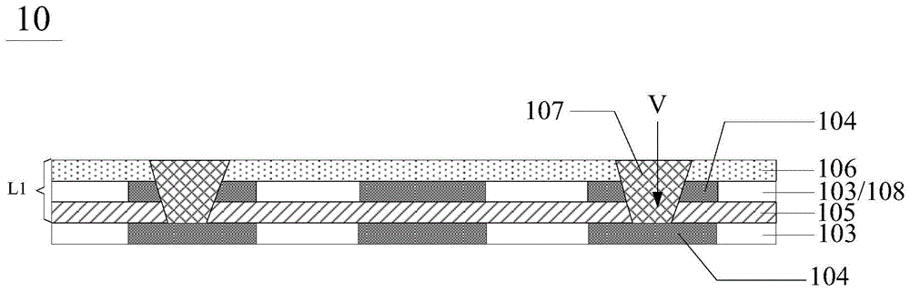
参见图11,图11示例性示出了采用本申请实施例提供的制备方法的所制备的封装载板的结构示意图。在该封装载板10中,可以包括:第一线路层和层叠于第一线路层上的叠层结构L1。其中,第一线路层可以包括第一介电层103和填充于第一介电层103的镂空区域内的金属走线104。叠层结构L1可以包括依次层叠设置的第二介电层105、第二线路层和第三介电层106,贯穿第三介电层106、第二线路层和第二介电层105的过孔,以及填充于过孔中的导电材料107;在该叠层结构L1中,第二线路层位于第二介电层105与第三介电层106之间,第二介电层106位于靠近第一线路层一侧;而第二线路层可以包括第四介电层108(即在制备过程中采用的第二线路基板中的第一介电层)和填充于第四介电层108的镂空区域内的金属走线104;第一线路层和与其相邻的叠层结构L1中的第二线路层可以通过过孔内的导电材料107电连接。Referring to FIG. 11 , FIG. 11 exemplarily shows a schematic structural diagram of a packaging carrier prepared by using the preparation method provided by the embodiment of the present application. The
本申请实施例提供的封装封板,第一方面,由于每一层金属走线是采用本申请提供的线路基板形成的,因此相比采用光刻工艺形成的线路层,本申请中形成的封装载板可以实现每一层金属走线的高精度。第二方面,由于金属走线已经嵌入在第一介电层中,因此位于相邻的金属走线层间的第三介电层,与在如图12所示的两层金属走线之间填充介电材料相比,可以使两层金属走线之间的介电材料的厚度更薄,即本申请中第三介电层只需要将两层金属走线隔开即可,而图12中的介电材料不仅需要满足填充同层金属走线之间的间隙,而且需要将两层金属走线隔开,因此需要的介电材料的量必须足够充足,从而导致两层金属走线之间的介电材料的厚度h较厚。因此,本申请的封装载板可以实现厚度较薄。第三方面,本申请中,利用第三介电层代替光刻胶,通过激光烧蚀工艺形成连通不同金属走线层的过孔,可以提高封装载板中过孔的精度,从而提升封装载板的整体线路精度。第四方面,本申请中过孔底部直接与金属走线接触,可以免去常规化学镀的步骤,且不必使用特殊的材料就可以在过孔内电镀导电材料,因此采用常规工艺和常规材料就可以实现,成本较低。In the package sealing plate provided by the embodiment of the present application, in the first aspect, since each layer of metal wiring is formed by using the circuit substrate provided by the application, compared with the circuit layer formed by the photolithography process, the package formed in the application The carrier board can realize the high precision of each layer of metal traces. In the second aspect, since the metal wiring has been embedded in the first dielectric layer, the third dielectric layer between the adjacent metal wiring layers and the two layers of metal wiring as shown in Figure 12 Compared with filling the dielectric material, the thickness of the dielectric material between the two layers of metal traces can be made thinner, that is, the third dielectric layer in this application only needs to separate the two layers of metal traces, and Figure 12 The dielectric material not only needs to fill the gap between the metal traces of the same layer, but also needs to separate the two layers of metal traces. Therefore, the amount of dielectric material required must be sufficient, so that the gap between the two layers of metal traces The thickness h of the dielectric material between them is thicker. Therefore, the packaging carrier of the present application can achieve a thinner thickness. In the third aspect, in this application, the third dielectric layer is used instead of photoresist, and vias connected to different metal wiring layers are formed by laser ablation process, which can improve the precision of the vias in the packaging substrate, thereby improving the packaging performance. The overall circuit accuracy of the board. In the fourth aspect, in this application, the bottom of the via hole is directly in contact with the metal trace, which can avoid the conventional electroless plating step, and can electroplate conductive materials in the via hole without using special materials. Therefore, using conventional processes and conventional materials is easy Achievable and low cost.
本申请上述实施例仅是以在封装载板中形成两层线路层为例进行说明,当然还可以在封装载板中形成多层线路层,在该封装载板中继续堆叠线路层的方法可以参见步骤S202至步骤206。下面以在该封装载板中继续堆叠一层线路层为例进行示意说明。The above-mentioned embodiments of the present application are only described by forming two layers of circuit layers in the package carrier as an example. Of course, multiple circuit layers can also be formed in the package carrier. The method of continuing to stack the circuit layers in the package carrier can be Refer to step S202 to step 206. In the following, a schematic description will be made by taking the continuous stacking of one circuit layer in the package carrier as an example.
进一步地,如图13所示,该制备方法还可以包括:Further, as shown in Figure 13, the preparation method may also include:
步骤S401、如图14a所示,提供一如图7所示的第三线路基板100c,以位于第一线路基板100a上方第二介电层105、第一介电层103、金属走线104、第三介电层106和导电材料107为第一堆叠结构L1;在第一堆叠结构L1和第三线路基板100c之间压合一层第二介电层105,且第三线路基板100c的载板101位于远离第一堆叠结构L1一侧。Step S401, as shown in FIG. 14a, provide a
步骤S402、如图14b所示,去除第三线路基板100c中的载板101和金属层102。Step S402, as shown in FIG. 14b, remove the
步骤S403、如图14c所示,在第三线路基板100c的第一介电层103上形成第三介电层106。Step S403, as shown in FIG. 14c, forming a third
步骤S404、如图14d所示,通过激光烧蚀工艺形成贯穿新形成的第三介电层106、第三线路基板100c中的金属走线104以及新形成的第二介电层105的过孔V;Step S404, as shown in FIG. 14d , forming vias through the newly formed third
步骤S405、如图14e所示,在过孔V中形成导电材料107,以使第二线路基板100b中的金属走线104与第三线路基板100c中的金属走线104电连接。Step S405 , as shown in FIG. 14 e , form a
其中步骤S401至步骤S405的具体实施方式可以参见步骤S202至步骤206,在此不在赘述。The specific implementation manners of step S401 to step S405 can refer to step S202 to step 206, which will not be repeated here.
依次类推,还可以在封装载板中继续形成线路层,在此不作赘述。By analogy, it is also possible to continue to form a circuit layer in the packaging substrate, which will not be repeated here.
参见图15,图15示例性示出了本申请实施例提供的另一种封装载板的结构示意图。在该封装载板10中,第一线路层上层叠有多层叠层结构Ln。其中,图15中以封装载板10中包括三层叠层结构L1~Ln为例进行示意。在每一层叠层结构Ln中,均可以包括依次层叠设置的第二介电层105、第二线路层和第三介电层106,贯穿第三介电层106、第二线路层和第二介电层105的过孔V,以及填充于过孔V中的导电材料107;任意相邻的两层叠层结构Ln和Ln+1中的第二线路层,通过该相邻的两层叠层结构Ln和Ln+1中的导电材料电连接。Referring to FIG. 15 , FIG. 15 exemplarily shows a schematic structural diagram of another packaging carrier provided by an embodiment of the present application. In the
参见图16,在该封装载板10中,距离第一线路层最远的叠层结构L1中,叠层结构L1中的过孔V包括贯穿第三介电层106的第一过孔V1,以及贯穿第二线路层中的金属走线和第二介电层105的第二过孔V2;第一过孔V1在第一线路层的正投影覆盖第二过孔V2在第一线路层的正投影,即第一过孔V1覆盖第二过孔V2,第一过孔V1的面积大于或等于第二过孔V2的面积。这样如图17所示,在过孔V中形成导电材料107后,可以增加封装载板10最外侧的过孔中的导电材料107的面积,从而增加封装载板10与其它电器件的导电接触面积。Referring to FIG. 16 , in the
这样,在制备时,在堆叠最后一层线路线时,在形成贯穿第三介电层、第二线路基板中的金属走线以及第二介电层的过孔时,如图16所示,可以先通过激光烧蚀工艺形成贯穿第三介电层106的第一过孔V1;然后通过激光烧蚀工艺形成贯穿第二介电层105和第二线路基板中的金属走线104的第二过孔V2,且第一过孔V1在第一线路基板(图16中仅视出了第一线路基板中的第一介电层103和金属走线104)的正投影覆盖第二过孔V2在第一线路基板的正投影。In this way, during preparation, when stacking the last layer of wiring lines, when forming via holes penetrating through the third dielectric layer, the metal wiring in the second circuit substrate, and the second dielectric layer, as shown in FIG. 16 , The first via hole V1 penetrating through the third
进一步地,在本申请中,如图18所示,在该封装载板10中,在每一层叠层结构Ln中,叠层结构Ln中的过孔V包括贯穿第三介电层106的第一过孔V1,以及贯穿第二线路层中的金属走线和第二介电层105的第二过孔V2;第一过孔V1在第一线路层的正投影覆盖第二过孔V2在第一线路层的正投影,这样,可以增大过孔V中导电材料107的上表面的面积,这样当导电材料107的上表面的面积增大后,在其上叠加叠层结构Ln时,即使叠层结构Ln中形成的过孔V位置发生一定误差,仍能够与导电材料107形成良好的接触。Further, in this application, as shown in FIG. 18 , in the
在本申请实施例提供的封装载板10中,如图18所示,第一介电层103中金属走线104的图形可以根据实际产品进行设计,在此不作限定。一般不同第一介电层103中的金属走线104的图形不相同,位于不同第一介电层103中的金属走线104可以通过过孔V中的导电材料107实现电连接。In the
进一步,在本申请中,在过孔V中形成导电材料107之后,还可以包括:去除第三介电层106以及位于所述第三介电层106的过孔内的导电材料107,即去除位于第二线路基板100b中的金属走线104上方的导电材料107。形成的封装载板如图19和图20所示,在封装载板10的叠层结构Ln中,仅包括第二介电层105和第二线路层,这样可以进一步降低封装载板的厚度。在具体实施时,可以是部分叠层结构Ln中不包括第三介电层,也可以是全部叠层结构中均不包括第三介电层,在此不作限定。Further, in this application, after forming the
在本申请中,在封装载板的两侧还可以包括阻焊层等,在此不作限定。In the present application, solder mask layers and the like may also be included on both sides of the package carrier board, which is not limited here.
可选的,在本申请中,为了提高材料的一致性,第一介电层、第二介电层、第三介电层和第四介电层中至少两层介电层的材料相同。当然,在具体实施时,不同的介电层也可以采用不同材料,在此不作限定。Optionally, in the present application, in order to improve the consistency of materials, the materials of at least two dielectric layers among the first dielectric layer, the second dielectric layer, the third dielectric layer and the fourth dielectric layer are the same. Of course, in specific implementation, different dielectric layers may also use different materials, which is not limited here.
可选的,在本申请中,不同线路层中的金属走线的材料相同。这样不同的线路层可以采用相同的工艺形成,从而可以降低成本。Optionally, in this application, the metal traces in different circuit layers are made of the same material. In this way, different circuit layers can be formed using the same process, thereby reducing costs.
当然,在具体实施时,不同线路层中的金属走线的材料也可以不相同。Certainly, during specific implementation, the materials of the metal traces in different circuit layers may also be different.
可选的,在本申请中,过孔中的导电材料与线路层中的金属走线的材料可以相同。Optionally, in this application, the conductive material in the via hole may be the same as the material of the metal wiring in the wiring layer.
相应的,如图21所示,本申请实施例还提供了一种封装结构3,包括上述任一种封装载板10,以及塑封于该封装载板10一侧的芯片20。由于该封装结构3解决问题的原理与前述一种封装载板10相似,因此该封装结构3的实施可以参见前述封装载板10的实施,重复之处不再赘述。Correspondingly, as shown in FIG. 21 , the embodiment of the present application also provides a
在一种可行的实现方式中,该封装结构可以通过以下步骤形成:In a feasible implementation, the encapsulation structure can be formed through the following steps:
步骤S501、如图22a所示,在制备封装载板10时,在第一线路基板100a上形成目标数量的线路层之后,在去除第一线路基板100a中的载板101和金属层102之前,在远离第一线路基板100a一侧绑定芯片20。Step S501, as shown in FIG. 22a, when preparing the
步骤S502、如图22b所示,采用塑封材料210塑封芯片20。In step S502 , as shown in FIG. 22 b , the
步骤S503、去除第一线路基板100a中的载板101和金属层102,从而形成如图21所示的封装结构3。Step S503 , removing the
进一步地,还可以在封装载板10背离芯片20一侧形成阻焊层等,在此不作限定。Further, a solder resist layer and the like may also be formed on the side of the
进一步地,如图23所示,还可以在封装载板10背离芯片20一侧植入焊球001,便于该封装结构3后续与电路板进行焊接。Further, as shown in FIG. 23 ,
相应的,如图24所示,本申请实施例还提供了另一种封装结构3,包括封装载板10,以及塑封于该封装载板10一侧的芯片20。该封装载板10中可以包括至少一层叠层结构Ln,图24中以封装载板10中包括两层叠层结构L1和L2为例进行示意。每一层叠层结构Ln中包括第二介电层105、线路层和第三介电层106,其中线路层中包括第一介电层103和填充于第一介电层103的镂空区域内的金属走线104。层叠层结构Ln具有贯穿第二介电层105、线路层的金属走线104和第三介电层106的过孔V,过孔V内填充有导电材料107。Correspondingly, as shown in FIG. 24 , the embodiment of the present application also provides another
在一种可行的实现方式中,该封装结构可以通过以下步骤形成:In a feasible implementation, the encapsulation structure can be formed through the following steps:
步骤S601、如图25a所示,采用塑封材料210塑封芯片20。In step S601 , as shown in FIG. 25 a , the
步骤S602、如图25b所示,在塑封材料210和线路基板100之间压合第二介电层105。Step S602 , as shown in FIG. 25 b , press-bond the
步骤S603、如图25c所示,去除线路基板100中的载板101和金属层102,在第一介电层103远离第二介电层105一侧形成第三介电层106,通过激光烧蚀工艺形成贯穿第三介电层106、线路基板100中的金属走线104以及第二介电层105的过孔,在过孔中形成导电材料107,从而形成一层叠层结构L1。Step S603, as shown in FIG. 25c, remove the
步骤S604、在叠层结构L1和线路基板100之间压合第二介电层105;去除线路基板100中的载板101和金属层102,在第一介电层103远离第二介电层105一侧形成第三介电层106,通过激光烧蚀工艺形成贯穿第三介电层106、线路基板100中的金属走线104以及第二介电层105的过孔V,在过孔V中形成导电材料107,从而形成第二层叠层结构L2,进而形成如图24所示的封装结构3,形成在封装结构3中的两层叠层结构L1和L2组成封装载板10。Step S604, pressing the
在具体实施时,当封装结构的封装载板中包括多层叠层结构时,可以重复步骤S604,直至形成目标层数的叠层结构,在此不作赘述。In a specific implementation, when the package carrier of the package structure includes a multi-layer laminated structure, step S604 may be repeated until a laminated structure with a target number of layers is formed, which will not be repeated here.
本申请对过孔中的导电材料不作限定,例如,导电材料可以为金、银、铜、铂、锡等。The present application does not limit the conductive material in the via hole, for example, the conductive material may be gold, silver, copper, platinum, tin or the like.
本申请对过孔内导电材料的形成方式不作限定,可以能够实现在过孔中形成导电材料的任何方式。示例性的,可以直接通过电镀方式在过孔中形成导电材料。The present application does not limit the method of forming the conductive material in the via hole, and any method can be used to form the conductive material in the via hole. Exemplarily, the conductive material may be directly formed in the via hole by electroplating.
进一步地,如图26所示,还可以在封装载板10背离芯片20一侧植入焊球001,便于该封装结构3后续与电路板进行焊接。Further, as shown in FIG. 26 ,
相应地,本申请还提供了一种电子设备,如图3所示,包括:壳体1、位于壳体1内的电路板2和封装结构3;该封装结构3位于电路板2上,且封装模组3与电路板2电连接。示例性的,该电路板可以为PCB。由于该电子设备解决问题的原理与前述一种封装结构3相似,因此该电子设备的实施可以参见前述封装结构3的实施,重复之处不再赘述。Correspondingly, the present application also provides an electronic device, as shown in FIG. 3 , comprising: a
显然,本领域的技术人员可以对本申请进行各种改动和变型而不脱离本申请的保护范围。这样,倘若本申请的这些修改和变型属于本申请权利要求及其等同技术的范围之内,则本申请也意图包含这些改动和变型在内。Apparently, those skilled in the art can make various changes and modifications to this application without departing from the protection scope of this application. In this way, if these modifications and variations of the present application fall within the scope of the claims of the present application and their equivalent technologies, the present application is also intended to include these modifications and variations.
Claims (19)
Priority Applications (1)
| Application Number | Priority Date | Filing Date | Title |
|---|---|---|---|
| PCT/CN2022/113348 WO2023071446A1 (en) | 2021-10-27 | 2022-08-18 | Package carrier, preparation method therefor, circuit substrate, package structure, and electronic device |
Applications Claiming Priority (2)
| Application Number | Priority Date | Filing Date | Title |
|---|---|---|---|
| CN202111258938X | 2021-10-27 | ||
| CN202111258938 | 2021-10-27 |
Publications (1)
| Publication Number | Publication Date |
|---|---|
| CN116031232A true CN116031232A (en) | 2023-04-28 |
Family
ID=86069484
Family Applications (1)
| Application Number | Title | Priority Date | Filing Date |
|---|---|---|---|
| CN202111536692.8A Pending CN116031232A (en) | 2021-10-27 | 2021-12-15 | Encapsulation carrier, its preparation method, circuit substrate, encapsulation structure and electronic equipment |
Country Status (2)
| Country | Link |
|---|---|
| CN (1) | CN116031232A (en) |
| WO (1) | WO2023071446A1 (en) |
Citations (4)
| Publication number | Priority date | Publication date | Assignee | Title |
|---|---|---|---|---|
| US8322030B1 (en) * | 2002-05-01 | 2012-12-04 | Amkor Technology, Inc. | Circuit-on-foil process for manufacturing a laminated semiconductor package substrate having embedded conductive patterns |
| CN103635027A (en) * | 2012-08-29 | 2014-03-12 | 深南电路有限公司 | A circuit board making method and the circuit board |
| CN106229309A (en) * | 2016-07-20 | 2016-12-14 | 日月光半导体(上海)有限公司 | Base plate for packaging and manufacture method thereof |
| US20200068721A1 (en) * | 2011-10-31 | 2020-02-27 | Unimicron Technology Corp. | Package structure and manufacturing method thereof |
Family Cites Families (3)
| Publication number | Priority date | Publication date | Assignee | Title |
|---|---|---|---|---|
| CN100593963C (en) * | 2007-07-17 | 2010-03-10 | 欣兴电子股份有限公司 | Embedded circuit structure and process thereof |
| CN101754578B (en) * | 2008-12-18 | 2012-07-18 | 欣兴电子股份有限公司 | Snap-in circuit structure and method of forming the same |
| CN111326419B (en) * | 2018-12-17 | 2021-12-03 | 北京梦之墨科技有限公司 | Method for manufacturing circuit |
-
2021
- 2021-12-15 CN CN202111536692.8A patent/CN116031232A/en active Pending
-
2022
- 2022-08-18 WO PCT/CN2022/113348 patent/WO2023071446A1/en not_active Ceased
Patent Citations (4)
| Publication number | Priority date | Publication date | Assignee | Title |
|---|---|---|---|---|
| US8322030B1 (en) * | 2002-05-01 | 2012-12-04 | Amkor Technology, Inc. | Circuit-on-foil process for manufacturing a laminated semiconductor package substrate having embedded conductive patterns |
| US20200068721A1 (en) * | 2011-10-31 | 2020-02-27 | Unimicron Technology Corp. | Package structure and manufacturing method thereof |
| CN103635027A (en) * | 2012-08-29 | 2014-03-12 | 深南电路有限公司 | A circuit board making method and the circuit board |
| CN106229309A (en) * | 2016-07-20 | 2016-12-14 | 日月光半导体(上海)有限公司 | Base plate for packaging and manufacture method thereof |
Also Published As
| Publication number | Publication date |
|---|---|
| WO2023071446A1 (en) | 2023-05-04 |
Similar Documents
| Publication | Publication Date | Title |
|---|---|---|
| EP2954760B1 (en) | Fusion bonded liquid crystal polymer circuit structure | |
| CN100403534C (en) | Microelectronic substrate with integrated devices and method of manufacturing the same | |
| CN100388467C (en) | Semiconductor package, manufacturing method thereof, and semiconductor device | |
| TWI466607B (en) | Printed circuit board having buried component and method for manufacturing same | |
| TWI507096B (en) | Multilayer printed circuit board and method for manufacturing same | |
| TWI538584B (en) | Embedded high density interconnection printed circuit board and method for manufactruing same | |
| CN101568226B (en) | Multi-layer flexible printed circuit board and method of manufacturing the same | |
| JP2014082493A (en) | Hybrid lamination substrate, manufacturing method thereof and package substrate | |
| CN1491076A (en) | Manufacturing method of wiring substrate | |
| US10159154B2 (en) | Fusion bonded liquid crystal polymer circuit structure | |
| US10506722B2 (en) | Fusion bonded liquid crystal polymer electrical circuit structure | |
| KR20090117237A (en) | Electronic circuit board and manufacturing method | |
| KR20150102504A (en) | Embedded board and method of manufacturing the same | |
| TWI389279B (en) | Circuit board structure and its manufacturing method | |
| CN102256450A (en) | Embedded circuit board of passive device and manufacturing method thereof | |
| CN114503790B (en) | Embedded circuit board and manufacturing method thereof | |
| CN111564414A (en) | Component carrier and method of making a component carrier | |
| JP5179856B2 (en) | Wiring board built-in component and manufacturing method thereof, wiring board | |
| US20190296102A1 (en) | Embedded component structure and manufacturing method thereof | |
| CN101192542A (en) | Circuit board structure and manufacturing method thereof | |
| KR20080055728A (en) | Capacitor Adhesive Sheet and Manufacturing Method of Capacitor-embedded Printed Wiring Board Using the Same | |
| WO2023087284A1 (en) | Packaging structure and preparation method therefor, packaging module, and electronic device | |
| CN102056398A (en) | Circuit board structure and manufacturing method thereof | |
| CN102045936B (en) | Circuit board structure | |
| WO2023071446A1 (en) | Package carrier, preparation method therefor, circuit substrate, package structure, and electronic device |
Legal Events
| Date | Code | Title | Description |
|---|---|---|---|
| PB01 | Publication | ||
| PB01 | Publication | ||
| SE01 | Entry into force of request for substantive examination | ||
| SE01 | Entry into force of request for substantive examination |