CN115989591A - Phosphor substrate, light emitting substrate and lighting device - Google Patents
Phosphor substrate, light emitting substrate and lighting device Download PDFInfo
- Publication number
- CN115989591A CN115989591A CN202180053059.5A CN202180053059A CN115989591A CN 115989591 A CN115989591 A CN 115989591A CN 202180053059 A CN202180053059 A CN 202180053059A CN 115989591 A CN115989591 A CN 115989591A
- Authority
- CN
- China
- Prior art keywords
- layer
- phosphor
- light
- substrate
- light emitting
- Prior art date
- Legal status (The legal status is an assumption and is not a legal conclusion. Google has not performed a legal analysis and makes no representation as to the accuracy of the status listed.)
- Withdrawn
Links
Images


Classifications
-
- H—ELECTRICITY
- H10—SEMICONDUCTOR DEVICES; ELECTRIC SOLID-STATE DEVICES NOT OTHERWISE PROVIDED FOR
- H10H—INORGANIC LIGHT-EMITTING SEMICONDUCTOR DEVICES HAVING POTENTIAL BARRIERS
- H10H20/00—Individual inorganic light-emitting semiconductor devices having potential barriers, e.g. light-emitting diodes [LED]
- H10H20/80—Constructional details
- H10H20/85—Packages
- H10H20/851—Wavelength conversion means
- H10H20/8514—Wavelength conversion means characterised by their shape, e.g. plate or foil
-
- H—ELECTRICITY
- H10—SEMICONDUCTOR DEVICES; ELECTRIC SOLID-STATE DEVICES NOT OTHERWISE PROVIDED FOR
- H10H—INORGANIC LIGHT-EMITTING SEMICONDUCTOR DEVICES HAVING POTENTIAL BARRIERS
- H10H20/00—Individual inorganic light-emitting semiconductor devices having potential barriers, e.g. light-emitting diodes [LED]
- H10H20/80—Constructional details
- H10H20/85—Packages
- H10H20/851—Wavelength conversion means
-
- H—ELECTRICITY
- H05—ELECTRIC TECHNIQUES NOT OTHERWISE PROVIDED FOR
- H05K—PRINTED CIRCUITS; CASINGS OR CONSTRUCTIONAL DETAILS OF ELECTRIC APPARATUS; MANUFACTURE OF ASSEMBLAGES OF ELECTRICAL COMPONENTS
- H05K3/00—Apparatus or processes for manufacturing printed circuits
- H05K3/22—Secondary treatment of printed circuits
- H05K3/28—Applying non-metallic protective coatings
-
- H—ELECTRICITY
- H10—SEMICONDUCTOR DEVICES; ELECTRIC SOLID-STATE DEVICES NOT OTHERWISE PROVIDED FOR
- H10H—INORGANIC LIGHT-EMITTING SEMICONDUCTOR DEVICES HAVING POTENTIAL BARRIERS
- H10H20/00—Individual inorganic light-emitting semiconductor devices having potential barriers, e.g. light-emitting diodes [LED]
- H10H20/01—Manufacture or treatment
- H10H20/036—Manufacture or treatment of packages
- H10H20/0364—Manufacture or treatment of packages of interconnections
-
- H—ELECTRICITY
- H10—SEMICONDUCTOR DEVICES; ELECTRIC SOLID-STATE DEVICES NOT OTHERWISE PROVIDED FOR
- H10H—INORGANIC LIGHT-EMITTING SEMICONDUCTOR DEVICES HAVING POTENTIAL BARRIERS
- H10H20/00—Individual inorganic light-emitting semiconductor devices having potential barriers, e.g. light-emitting diodes [LED]
- H10H20/80—Constructional details
- H10H20/85—Packages
- H10H20/851—Wavelength conversion means
- H10H20/8511—Wavelength conversion means characterised by their material, e.g. binder
- H10H20/8512—Wavelength conversion materials
-
- H—ELECTRICITY
- H10—SEMICONDUCTOR DEVICES; ELECTRIC SOLID-STATE DEVICES NOT OTHERWISE PROVIDED FOR
- H10H—INORGANIC LIGHT-EMITTING SEMICONDUCTOR DEVICES HAVING POTENTIAL BARRIERS
- H10H20/00—Individual inorganic light-emitting semiconductor devices having potential barriers, e.g. light-emitting diodes [LED]
- H10H20/80—Constructional details
- H10H20/85—Packages
- H10H20/857—Interconnections, e.g. lead-frames, bond wires or solder balls
-
- H10W90/00—
-
- H—ELECTRICITY
- H10—SEMICONDUCTOR DEVICES; ELECTRIC SOLID-STATE DEVICES NOT OTHERWISE PROVIDED FOR
- H10H—INORGANIC LIGHT-EMITTING SEMICONDUCTOR DEVICES HAVING POTENTIAL BARRIERS
- H10H20/00—Individual inorganic light-emitting semiconductor devices having potential barriers, e.g. light-emitting diodes [LED]
- H10H20/01—Manufacture or treatment
- H10H20/036—Manufacture or treatment of packages
- H10H20/0361—Manufacture or treatment of packages of wavelength conversion means
Landscapes
- Engineering & Computer Science (AREA)
- Microelectronics & Electronic Packaging (AREA)
- Manufacturing & Machinery (AREA)
- Led Device Packages (AREA)
- Power Engineering (AREA)
- Physics & Mathematics (AREA)
- Condensed Matter Physics & Semiconductors (AREA)
- General Physics & Mathematics (AREA)
- Computer Hardware Design (AREA)
- Fastening Of Light Sources Or Lamp Holders (AREA)
- Planar Illumination Modules (AREA)
Abstract
本发明的荧光体基板供至少一个发光元件(20)搭载,该荧光体基板具备:绝缘基板(32);电路图案层(34),其配置于上述绝缘基板(32)的一面,并与上述至少一个发光元件(20)接合;荧光体层(36),其配置于上述绝缘基板(32)的一面侧,并包含以上述至少一个发光元件(20)的发光为激励光时的发光峰值波长位于可见光区域的荧光体;以及支承层(35),其配置在上述绝缘基板(32)与上述荧光体层(36)之间,该支承层(35)是不包含上述荧光体的层,且对上述荧光体层(36)进行支承。

The phosphor substrate of the present invention is mounted on at least one light-emitting element (20), and the phosphor substrate includes: an insulating substrate (32); a circuit pattern layer (34), which is arranged on one side of the insulating substrate (32) At least one light-emitting element (20) is bonded; a phosphor layer (36) is disposed on one side of the insulating substrate (32) and includes an emission peak wavelength when the emission of the at least one light-emitting element (20) is used as excitation light a phosphor located in the visible light region; and a support layer (35) disposed between the insulating substrate (32) and the phosphor layer (36), the support layer (35) being a layer not containing the phosphor, and The phosphor layer (36) is supported.
Description
技术领域technical field
本发明涉及荧光体基板、发光基板以及照明装置。The present invention relates to a phosphor substrate, a light emitting substrate, and a lighting device.
背景技术Background technique
专利文献1中公开了一种LED照明器具,其具备搭载了发光元件(LED元件)的基板。该LED照明器具在基板的表面设置反射材料,使发光效率提高。Patent Document 1 discloses an LED lighting fixture including a substrate on which a light emitting element (LED element) is mounted. In the LED illuminating device, a reflective material is arranged on the surface of the substrate, so that the luminous efficiency is improved.
专利文献1:中国专利公开106163113号公报Patent Document 1: Chinese Patent Publication No. 106163113
然而,在专利文献1所公开的结构的情况下,无法利用反射材料将LED照明器具发出的光调整为与发光元件发出的光不同的发光颜色的光,并且炫光对策不充分。However, in the case of the structure disclosed in Patent Document 1, the reflective material cannot be used to adjust the light emitted by the LED lighting fixture to light of a light emission color different from the light emitted by the light emitting element, and measures against glare are insufficient.
发明内容Contents of the invention
本发明的目的在于,提供一种荧光体基板,在搭载了发光元件的情况下,能够减少发光元件发出的光的炫光。An object of the present invention is to provide a phosphor substrate capable of reducing glare of light emitted by a light-emitting element when mounted thereon.
本发明的第一方式的荧光体基板供至少一个发光元件搭载,该荧光体基板具备:绝缘基板;电路图案层,其配置于上述绝缘基板的一面,并与上述至少一个发光元件接合;荧光体层,其配置于上述绝缘基板的一面侧,并包含以上述至少一个发光元件的发光为激励光时的发光峰值波长位于可见光区域的荧光体;以及支承层,其配置在上述绝缘基板与上述荧光体层之间,该支承层是不包含上述荧光体的层,且对所述荧光体层进行支承。A phosphor substrate according to a first aspect of the present invention mounts at least one light-emitting element, and the phosphor substrate includes: an insulating substrate; a circuit pattern layer disposed on one surface of the insulating substrate and bonded to the at least one light-emitting element; a phosphor a layer disposed on one side of the insulating substrate, and including a phosphor whose emission peak wavelength is in the visible light region when the emission of the at least one light-emitting element is used as excitation light; and a support layer disposed on the insulating substrate and the phosphor. Between the body layers, the support layer is a layer not containing the above-mentioned phosphor, and supports the phosphor layer.
在上述荧光体基板的基础上,在本发明的第二方式的荧光体基板中,上述支承层为包含白色颜料的单层构造。In addition to the phosphor substrate described above, in a phosphor substrate according to a second aspect of the present invention, the support layer has a single-layer structure containing a white pigment.
在上述荧光体基板的基础上,在本发明的第三方式的荧光体基板中,上述支承层进一步还配置在上述电路图案层中的除与上述至少一个发光元件接合的部分以外的部分和上述荧光体层之间。In addition to the phosphor substrate described above, in the phosphor substrate according to a third aspect of the present invention, the support layer is further disposed on a portion of the circuit pattern layer other than a portion bonded to the at least one light emitting element and the between phosphor layers.
在上述荧光体基板的基础上,在本发明的第四方式的荧光体基板中,上述支承层为与上述荧光体层邻接的邻接层包含白色颜料的多层构造。In addition to the phosphor substrate described above, in a phosphor substrate according to a fourth aspect of the present invention, the support layer has a multilayer structure in which an adjacent layer adjacent to the phosphor layer contains a white pigment.
在上述荧光体基板的基础上,在本发明的第五方式的荧光体基板中,上述支承层由上述邻接层和基层构成,该基层配置在上述绝缘基板与上述邻接层之间,不包含上述白色颜料,上述邻接层的厚度比上述基层的厚度薄。In addition to the phosphor substrate described above, in a phosphor substrate according to a fifth aspect of the present invention, the supporting layer is composed of the adjacent layer and a base layer, and the base layer is arranged between the insulating substrate and the adjacent layer and does not include the above-mentioned In the white pigment, the thickness of the above-mentioned adjacent layer is thinner than the thickness of the above-mentioned base layer.
在上述荧光体基板的基础上,在本发明的第六方式的荧光体基板中,上述邻接层进一步还配置在上述电路图案层中的除与上述至少一个发光元件接合的部分以外的部分和上述荧光体层之间。In addition to the phosphor substrate described above, in a phosphor substrate according to a sixth aspect of the present invention, the adjacent layer is further disposed on a portion of the circuit pattern layer other than a portion bonded to the at least one light emitting element and the between phosphor layers.
在上述荧光体基板的基础上,本发明的第七方式的荧光体基板在第二~第四方式中任一项所述的荧光体基板中,上述荧光体由多个荧光体粒子构成,上述白色颜料由多个白色粒子构成,上述多个荧光体粒子的、通过激光衍射散射法测定的体积基准的中值直径(D50)亦即D150与上述多个白色粒子的、通过激光衍射散射法测定的体积基准的中值直径(D50)亦即D250具有下述(式1)的关系,In addition to the phosphor substrate described above, the phosphor substrate according to a seventh aspect of the present invention is the phosphor substrate according to any one of the second to fourth aspects, wherein the phosphor is composed of a plurality of phosphor particles, and The white pigment is composed of a plurality of white particles, and the volume-based median diameter (D 50 ) of the plurality of phosphor particles measured by the laser diffraction scattering method, that is, D1 50 , is different from the volume-based median diameter (D 50 ) of the plurality of white particles measured by the laser diffraction scattering method. The volume-based median diameter (D 50 ), that is, D2 50 , which is determined by the method, has the following relationship (Formula 1),
(式1)0.8≤D250/D150≤1.2。(Formula 1) 0.8≤D2 50 /D1 50 ≤1.2.
在上述荧光体基板的基础上,在本发明的第八方式的荧光体基板中,上述荧光体层的厚度比上述支承层的厚度薄。In addition to the phosphor substrate described above, in a phosphor substrate according to an eighth aspect of the present invention, the thickness of the phosphor layer is thinner than the support layer.
在上述荧光体基板的基础上,在本发明的第九方式的荧光体基板中,上述荧光体层的外表面位于比上述电路图案层的外表面靠上述绝缘基板的厚度方向的外侧的位置。In addition to the phosphor substrate described above, in a phosphor substrate according to a ninth aspect of the present invention, an outer surface of the phosphor layer is located on an outer side in a thickness direction of the insulating substrate than an outer surface of the circuit pattern layer.
在上述荧光体基板的基础上,在本发明的第十方式的荧光体基板中,上述至少一个发光元件为多个发光元件。In addition to the phosphor substrate described above, in a phosphor substrate according to a tenth aspect of the present invention, the at least one light emitting element is a plurality of light emitting elements.
本发明的一个方式的发光基板具备上述荧光体基板和上述至少一个发光元件。A light-emitting substrate according to one aspect of the present invention includes the above-mentioned phosphor substrate and the above-mentioned at least one light-emitting element.
本发明的一个方式的照明装置具备上述发光基板和供给用于使上述至少一个发光元件发光的电力的电源。A lighting device according to one aspect of the present invention includes the above-mentioned light-emitting substrate and a power supply for supplying electric power for causing the above-mentioned at least one light-emitting element to emit light.
附图说明Description of drawings
图1A是第一实施方式的发光基板的俯视图。FIG. 1A is a plan view of a light emitting substrate according to a first embodiment.
图1B是第一实施方式的发光基板的仰视图。Fig. 1B is a bottom view of the light emitting substrate of the first embodiment.
图1C是通过图1A的1C-1C剖切线进行了剖切的发光基板的局部剖视图。FIG. 1C is a partial cross-sectional view of the light-emitting substrate cut along
图2A是第一实施方式的荧光体基板(省略荧光体层及支承层)的俯视图。FIG. 2A is a plan view of a phosphor substrate (a phosphor layer and a supporting layer are omitted) of the first embodiment.
图2B是第一实施方式的荧光体基板的俯视图。Fig. 2B is a plan view of the phosphor substrate of the first embodiment.
图3A是第一实施方式的发光基板的制造方法中的第一工序的说明图。3A is an explanatory diagram of a first step in the method of manufacturing the light-emitting substrate according to the first embodiment.
图3B是第一实施方式的发光基板的制造方法中的第二工序的说明图。3B is an explanatory diagram of a second step in the method of manufacturing the light-emitting substrate according to the first embodiment.
图3C是第一实施方式的发光基板的制造方法中的第三工序的说明图。3C is an explanatory diagram of a third step in the method of manufacturing the light-emitting substrate according to the first embodiment.
图3D是第一实施方式的发光基板的制造方法中的第四工序的说明图。3D is an explanatory diagram of a fourth step in the method of manufacturing the light-emitting substrate according to the first embodiment.
图3E是第一实施方式的发光基板的制造方法中的第五工序的说明图。3E is an explanatory diagram of a fifth step in the method of manufacturing the light-emitting substrate according to the first embodiment.
图4是用于对第一实施方式的发光基板的发光动作进行说明的图。FIG. 4 is a diagram for explaining the light emitting operation of the light emitting substrate according to the first embodiment.
图5是用于对比较方式的发光基板的发光动作进行说明的图。FIG. 5 is a diagram for explaining the light-emitting operation of the light-emitting substrate of the comparative embodiment.
图6是第二实施方式的发光基板的局部剖视图。Fig. 6 is a partial cross-sectional view of a light emitting substrate according to a second embodiment.
图7A是第二实施方式的发光基板的制造方法中的第二工序的说明图。7A is an explanatory diagram of a second step in the method of manufacturing the light-emitting substrate according to the second embodiment.
图7B是第二实施方式的发光基板的制造方法中的第三工序的说明图。7B is an explanatory diagram of a third step in the method of manufacturing the light-emitting substrate according to the second embodiment.
图7C是第二实施方式的发光基板的制造方法中的第四工序的说明图。7C is an explanatory diagram of a fourth step in the method of manufacturing the light-emitting substrate according to the second embodiment.
图7D是第二实施方式的发光基板的制造方法中的第五工序的说明图。7D is an explanatory diagram of a fifth step in the method of manufacturing the light-emitting substrate according to the second embodiment.
图8是第三实施方式的发光基板的局部剖视图。Fig. 8 is a partial cross-sectional view of a light emitting substrate according to a third embodiment.
图9A是第三实施方式的发光基板的制造方法中的第二工序的前半部分的说明图。9A is an explanatory diagram of the first half of the second step in the method of manufacturing the light-emitting substrate according to the third embodiment.
图9B是第三实施方式的发光基板的制造方法中的第二工序的后半部分的说明图。9B is an explanatory diagram of the second half of the second step in the method of manufacturing the light-emitting substrate according to the third embodiment.
图9C是第三实施方式的发光基板的制造方法中的第三工序的说明图。9C is an explanatory diagram of a third step in the method of manufacturing the light-emitting substrate according to the third embodiment.
图9D是第三实施方式的发光基板的制造方法中的第四工序的说明图。9D is an explanatory diagram of a fourth step in the method of manufacturing the light-emitting substrate according to the third embodiment.
图9E是第三实施方式的发光基板的制造方法中的第五工序的说明图。9E is an explanatory diagram of a fifth step in the method of manufacturing the light-emitting substrate according to the third embodiment.
图10是第四实施方式的发光基板的局部剖视图。Fig. 10 is a partial cross-sectional view of a light emitting substrate according to a fourth embodiment.
图11A是第四实施方式的发光基板的制造方法中的第一工序的后半部分的说明图。11A is an explanatory diagram of the second half of the first step in the method of manufacturing the light-emitting substrate according to the fourth embodiment.
图11B是第四实施方式的发光基板的制造方法中的第二工序的说明图。11B is an explanatory diagram of a second step in the method of manufacturing the light-emitting substrate according to the fourth embodiment.
图11C是第四实施方式的发光基板的制造方法中的第三工序的说明图。11C is an explanatory diagram of a third step in the method of manufacturing the light-emitting substrate according to the fourth embodiment.
图11D是第四实施方式的发光基板的制造方法中的第四工序的说明图。11D is an explanatory diagram of a fourth step in the method of manufacturing the light-emitting substrate according to the fourth embodiment.
图11E是第四实施方式的发光基板的制造方法中的第五工序的说明图。11E is an explanatory diagram of a fifth step in the method of manufacturing the light-emitting substrate according to the fourth embodiment.
图12是第五实施方式的发光基板的局部剖视图。Fig. 12 is a partial cross-sectional view of a light emitting substrate according to a fifth embodiment.
图13A是第五实施方式的发光基板的制造方法中的第二工序的前半部分的说明图。13A is an explanatory diagram of the first half of the second step in the method of manufacturing the light-emitting substrate according to the fifth embodiment.
图13B是第五实施方式的发光基板的制造方法中的第二工序的后半部分的说明图。13B is an explanatory diagram of the second half of the second step in the method of manufacturing the light-emitting substrate according to the fifth embodiment.
图13C是第五实施方式的发光基板的制造方法中的第三工序的说明图。13C is an explanatory diagram of a third step in the method of manufacturing the light-emitting substrate according to the fifth embodiment.
图13D是第五实施方式的发光基板的制造方法中的第四工序的说明图。13D is an explanatory diagram of a fourth step in the method of manufacturing the light-emitting substrate according to the fifth embodiment.
图13E是第五实施方式的发光基板的制造方法中的第五工序的说明图。13E is an explanatory diagram of a fifth step in the method of manufacturing the light-emitting substrate according to the fifth embodiment.
具体实施方式Detailed ways
《概要》"summary"
对作为本发明的一个例子的第一~第五实施方式按照它们的记载顺序进行说明。接着,对这些实施方式的变形例进行说明。此外,在以下的说明中参照的所有附图中,对相同的构成要素标注相同的附图标记,适当省略说明。The first to fifth embodiments which are examples of the present invention will be described in order of their description. Next, modifications of these embodiments will be described. In addition, in all the drawings referred to in the following description, the same reference numerals are attached to the same components, and descriptions thereof are appropriately omitted.
《第一实施方式》"First Embodiment"
以下,参照图1A~图5对第一实施方式进行说明。首先,参照图1A~图1C对本实施方式的发光基板10的结构及功能进行说明。接着,参照图3A~图3E对本实施方式的发光基板10的制造方法进行说明。接着,参照图4对本实施方式的发光基板10的发光动作进行说明。接着,参照图4、图5等对本实施方式的效果进行说明。Hereinafter, a first embodiment will be described with reference to FIGS. 1A to 5 . First, the structure and function of the light-emitting
此外,本实施方式的荧光体基板30是本实施方式的发光基板10的构成要素,因此在本实施方式的发光基板10的结构及功能的说明中进行说明。In addition, since the
<第一实施方式的发光基板的结构及功能><Structure and Function of the Light-Emitting Substrate of the First Embodiment>
图1A是本实施方式的发光基板10的俯视图(从表面31A侧观察得到的图),图1B是本实施方式的发光基板10的仰视图(从背面33A侧观察得到的图)。图1C是通过图1A的1C-1C剖切线进行了剖切的发光基板10的局部剖视图。1A is a top view of
本实施方式的发光基板10从表面31A侧及背面33A侧观察,作为一个例子是矩形。另外,本实施方式的发光基板10具备多个发光元件20、荧光体基板30、以及连接器、驱动IC等电子部件(省略图示)。即,本实施方式的发光基板10在荧光体基板30搭载了多个发光元件20及上述电子部件。The light-emitting
本实施方式的发光基板10具有若经由连接器从外部电源(省略图示)被供电则进行发光的功能。因此,本实施方式的发光基板10例如被利用为照明装置(省略图示)等中的主要光学部件。The light-emitting
此外,在以下的说明中详细地进行说明,但本实施方式的荧光体基板30及发光基板10的基本结构分别如下。In addition, although it demonstrates in detail in the following description, the basic structures of the
·本实施方式的荧光体基板的基本结构・Basic structure of the phosphor substrate of this embodiment
本实施方式的荧光体基板30是供至少一个发光元件20搭载的荧光体基板30,具备:绝缘层32(绝缘基板的一个例子);电路图案层34,其配置于绝缘层32的表面31(一面的一个例子),并与至少一个发光元件20接合;荧光体层36,其配置于绝缘层32的表面31侧,包含以至少一个发光元件20的发光为激励光时的发光峰值波长位于可见光区域的荧光体;以及支承层35,其配置在绝缘层32与荧光体层36之间,且是不包含上述荧光体的层,并支承荧光体层36。The
·本实施方式的发光基板的基本结构・Basic structure of the light-emitting substrate of this embodiment
另外,本实施方式的发光基板10具备具有上述的基本结构的荧光体基板30和至少一个发光元件20。In addition, the light-emitting
〔多个发光元件〕[multiple lighting elements]
多个发光元件20分别作为一个例子是装入有倒装芯片LED22(以下称为LED22。)的CSP(Chip Scale Package:芯片尺寸封装)(参照图1C)。如图1A所示,多个发光元件20以遍及荧光体基板30的表面31A侧的整体规则排列的状态搭载于荧光体基板30。各发光元件20发出的光的相关色温作为一个例子是3,018K。此外,在本实施方式中,构成为通过使用散热器(省略图示)、冷却风扇(省略图示),在多个发光元件20的发光动作时,以将荧光体基板30作为一个例子控制在常温到50℃~100℃的方式进行散热(冷却)。Each of the plurality of
另外,LED22的结电平JL设定在高于荧光体层36的表面的电平的位置。Moreover, the junction level JL of LED22 is set to the position higher than the level of the surface of the
这里,若对本说明书中使用于数值范围的“~”的意思进行补充,则例如“50℃~100℃”意味着“50℃以上100℃以下”。即,本说明书中使用于数值范围的“~”意味着“《~》之前的记载部分以上《~》之后的记载部分以下”。Here, when the meaning of "to" used in the numerical range in this specification is supplemented, for example, "50°C to 100°C" means "50°C to 100°C". That is, "-" used for a numerical range in this specification means "more than the description part before "-" and below the description part after "-".
〔荧光体基板〕〔Phosphor substrate〕
图2A是本实施方式的荧光体基板30的图,且是省略支承层35及荧光体层36而图示的俯视图(从表面31A侧观察得到的图)。图2B是本实施方式的荧光体基板30的俯视图(从背面33A侧观察得到的图)。此外,本实施方式的荧光体基板30的仰视图与从背面33A侧观察发光基板10得到的图相同。另外,本实施方式的荧光体基板30的局部剖视图与从图1C的局部剖视图除去发光元件20之后的情况的图相同。即,本实施方式的荧光体基板30从表面31A侧及背面33A侧观察作为一个例子是矩形。2A is a diagram of
此外,在图2A中,图示了后述的多个电极对34A、和作为多个电极对34A以外的部分的配线部分34B的范围,但实际上,由于两者形成于同一平面(外表面),所以在图2A那样除去支承层35及荧光体层36之后的图中,不存在两者的边界。然而,图2A是为了明确两者的位置关系而适当地加入了多个电极对34A及配线部分34B的附图标记的图。In addition, in FIG. 2A, the range of a plurality of
本实施方式的荧光体基板30具备绝缘层32、电路图案层34、支承层35、荧光体层36及背面图案层38(参照图1B、图1C、图2A及图2B)。在图2A中,省略了支承层35及荧光体层36,但如图2B所示,荧光体层36作为一个例子配置于绝缘层32的表面31侧。具体而言,如图1C所示,荧光体层36作为一个例子配置为覆盖支承层35的与绝缘层32相反的一侧的面、和电路图案层34的除后述的多个电极对34A以外的部分。另外,支承层35配置于绝缘层32的表面31中的、除配置有电路图案层34的部分以外的部分,且配置在绝缘层32与荧光体层36之间(参照图1C及图3E)。
另外,如图1B及图2A所示,在荧光体基板30的四个角附近的4处及中央附近的2处的合计6处形成有贯通孔39。6处贯通孔39在荧光体基板30及发光基板10的制造时被利用为定位孔。另外,6处贯通孔39被利用为用于确保向(发光)灯具框体的散热效果(防止基板翘曲及浮起)的安装用的螺孔。此外,本实施方式的荧光体基板30如后述那样,通过对在绝缘板的两面设置有铜箔层的双面板(以下称为母板MB。参照图3A)进行蚀刻等加工来制造。作为该母板MB的一个例子,可举出利昌工业株式会社制的CS-3305A。In addition, as shown in FIG. 1B and FIG. 2A , through-
〈绝缘层〉<Insulation>
以下,对本实施方式的绝缘层32的主要特征进行说明。Hereinafter, main features of the insulating
形状如上述那样,作为一个例子从表面31侧及背面33侧观察为矩形。As described above, the shape is, as an example, rectangular when viewed from the side of the
材质作为一个例子是包含双马来酰亚胺(Bismaleimide)树脂及玻璃布的绝缘材料。An example of the material is an insulating material including bismaleimide resin and glass cloth.
厚度作为一个例子是100μm。The thickness is 100 μm as an example.
纵向及横向的热膨胀系数(CTE)分别作为一个例子在50℃~100℃的范围内为10ppm/℃以下。另外,从另一个角度来看,纵向及横向的热膨胀系数(CTE)分别作为一个例子是6ppm/K。该值与本实施方式的发光元件20的情况几乎相等(90%~110%、即±10%以内)。The coefficients of thermal expansion (CTE) in the longitudinal direction and in the transverse direction are, for example, 10 ppm/°C or less in the range of 50°C to 100°C. In addition, from another point of view, the longitudinal and transverse coefficients of thermal expansion (CTE) are 6 ppm/K as an example. This value is almost equal to that of the light-emitting
玻璃化转变温度作为一个例子高于300℃。The glass transition temperature is higher than 300° C. as an example.
储能模量作为一个例子在100℃~300℃的范围内大于1.0×10¹⁰Pa小于1.0×10¹¹Pa。As an example, the storage modulus is more than 1.0×10 10 Pa and less than 1.0×10 11 Pa in the range of 100°C to 300°C.
纵向及横向的弯曲模量作为一个例子分别在常态下为35GPa及34GPa。The longitudinal and transverse flexural moduli are, for example, 35 GPa and 34 GPa under normal conditions, respectively.
纵向及横向的热弯曲模量作为一个例子在250℃下为19GPa。As an example, the thermal flexural modulus in the longitudinal and transverse directions is 19 GPa at 250°C.
吸水率作为一个例子在23℃的温度环境下放置了24小时的情况下为0.13%。As an example, the water absorption rate is 0.13% when left in a temperature environment of 23° C. for 24 hours.
相对介电常数作为一个例子在1MHz常态下为4.6。As an example, the relative permittivity is 4.6 under normal conditions of 1 MHz.
介质损耗角正切作为一个例子在1MHz常态下为0.010。As an example, the dielectric loss tangent is 0.010 at 1MHz.
〈电路图案层〉<Circuit pattern layer>
本实施方式的电路图案层34是设置于绝缘层32的表面31的金属层,作为一个例子是铜箔层(Cu制的层),与接合于连接器(省略图示)的端子37导通。而且,电路图案层34在构成发光基板10的状态下将经由连接器从外部电源(省略图示)被供电的电力向多个发光元件20供给。因此,电路图案层34的一部分成为将多个发光元件20分别接合的多个电极对34A。即,电路图案层34配置于绝缘层32的表面31,并与各发光元件20连接。另外,若从另一个角度来看,则电路图案层34配置于绝缘层32的表面31,通过作为各电极对34A的外表面的接合面34A1与各发光元件20连接。The
另外,如上述那样,由于多个发光元件20遍及绝缘层32的表面31侧的整体规则排列(参照图1A),所以多个电极对34A也遍及表面31侧的整体规则地排列(参照图2A)。这里,在本说明书中,将电路图案层34中的除多个电极对34A以外的部分称为配线部分34B。另外,将配线部分34B的外表面称为非接合面34B1(电路图案层34的外表面中的除接合面34A1以外的部分)。非接合面34B1是电路图案层34中的除接合于所有发光元件20的部分以外的部分。In addition, as described above, since the plurality of
此外,从表面31侧观察,电路图案层34相对于绝缘层32的表面31所占的比例(电路图案层34的专有面积)作为一个例子为绝缘层32的表面31的60%以上(参照图2A)。另外,在本实施方式中,电路图案层34的厚度作为一个例子为175μm。不过,在各图中,电路图案层34的厚度、绝缘层32的厚度、荧光体层36的厚度等的关系与尺寸不一致。In addition, when viewed from the
〈支承层〉<support layer>
本实施方式的支承层35如上述那样,配置于绝缘层32的表面31中的、除配置有电路图案层34的部分以外的部分,并支承荧光体层36的一部分(参照图1C及图3E)。这里,支承层35支承的荧光体层36的一部分是指荧光体层36中的除配置于电路图案层34的外表面的部分以外的部分。此外,如图1C、图3E等所示,支承层35的厚度作为一个例子设定为与电路图案层34的厚度相同,但并不局限于此,可以设定为较薄,相反也可以设定为较厚。The supporting
本实施方式的支承层35与后述的荧光体层36不同,不包含荧光体(多个荧光体粒子的集合体),作为一个例子包含白色颜料(多个白色粒子的集合体)和粘合剂,是多个白色粒子分散在该粘合剂中的绝缘层。另外,本实施方式的支承层35作为一个例子为单层构造。这里,多个白色粒子作为一个例子为氧化钛,但也可以是氧化钙、其他白色粒子。另外,粘合剂例如为环氧系、丙烯酸酯系、硅酮系等的粘合剂,只要具有与阻焊剂所包含的粘合剂同等的绝缘性即可。The
此外,如上述那样,支承层35配置在绝缘层32与荧光体层36之间(参照图1C、图3E等)。另外,针对支承层35包含白色颜料的技术意义,在后述的第一实施方式的效果的说明中进行说明。In addition, as described above, the supporting
〈荧光体层〉<Phosphor layer>
如图2B及图3E所示,本实施方式的荧光体层36作为一个例子,配置于支承层35的与绝缘层32相反的一侧的面(在图示中为上侧的面)、以及电路图案层34中的非接合面34B1。若从另一个角度来看,则荧光体层36配置为留下支承层35及电路图案层34的电极对34A,而覆盖绝缘层32的表面31侧。在本实施方式中,从表面31侧观察,荧光体层36相对于绝缘层32的表面31所占的比例作为一个例子相对于绝缘层32的表面31的面积为80%以上。As shown in FIG. 2B and FIG. 3E , as an example,
此外,荧光体层36中的绝缘层32的厚度方向的外侧的面(外表面)位于比电路图案层34中的绝缘层32的厚度方向的外侧的面(外表面)靠该厚度方向的外侧(参照图1C及图3E)。另外,荧光体层36中的、配置于支承层35的部分的外表面以及配置于电路图案层34的部分的外表面作为一个例子,位于相同高度、即绝缘层32的厚度方向的相同位置(参照图3E)。In addition, the outer surface (outer surface) in the thickness direction of the insulating
本实施方式的荧光体层36作为一个例子包含后述的荧光体(多个荧光体粒子的集合体)和粘合剂,是多个荧光体粒子分散在该粘合剂中的绝缘层。荧光体层36所包含的荧光体具有以各发光元件20的发光为激励光进行激励的性质。具体而言,本实施方式的荧光体具有以发光元件20的发光为激励光时的发光峰值波长位于可见光区域的性质。此外,该粘合剂例如为环氧系、丙烯酸酯系、硅酮系等的粘合剂,只要是具有与阻焊剂所包含的粘合剂同等的绝缘性的材料即可。The
这里,在本说明书中,将荧光体层36所包含的多个荧光体粒子的、通过激光衍射散射法测定的体积基准的中值直径(D50)标记为D150。另外,将上述的支承层35所包含的多个白色粒子的、通过激光衍射散射法测定的体积基准的中值直径(D50)标记为D250。于是,在本实施方式的荧光体基板30中,D150与D250作为一个例子具有下述(式1)的关系。Here, in this specification, the volume-based median diameter (D 50 ) of the plurality of phosphor particles contained in the
(式1)0.8≤D250/D150≤1.2(Formula 1) 0.8≤D2 50 /D1 50 ≤1.2
即,在本实施方式中,构成白色颜料的多个白色粒子的中值直径(D50)相对于构成荧光体的多个荧光体粒子的中值直径(D50)被设定为80%以上120%以下的范围。That is, in this embodiment, the median diameter (D 50 ) of the plurality of white particles constituting the white pigment is set to 80% or more of the median diameter (D 50 ) of the plurality of phosphor particles constituting the phosphor. range below 120%.
(荧光体的具体例)(Specific example of phosphor)
这里,本实施方式的荧光体层36所包含的荧光体作为一个例子,为从由含有Eu的α型塞隆荧光体、含有Eu的β型塞隆荧光体、含有Eu的CASN荧光体及含有Eu的SCASN荧光体构成的组中选择出的至少1种荧光体。此外,上述的荧光体为本实施方式中的一个例子,如YAG、LuAG、BOS其他可见光激励的荧光体那样,也可以是除上述的荧光体以外的荧光体。Here, the phosphor contained in the
含有Eu的α型塞隆荧光体用通式:MxEuySi12-(m+n)Al(m+n)OnN16-n表示。上述通式中,M是从由Li、Mg、Ca、Y及镧系元素(其中,La和Ce除外)构成的组中选择出的、至少包含Ca的1种以上的元素,在将M的价数设为a时,为ax+2y=m,x为0<x≤1.5,0.3≤m<4.5,0<n<2.25。The Eu-containing α-sialon phosphor is represented by the general formula: M x Eu y Si 12-(m+n) Al (m+n) On N 16-n . In the above general formula, M is selected from the group consisting of Li, Mg, Ca, Y, and lanthanoid elements (except for La and Ce), and at least includes one or more elements of Ca. When the valence is set to a, ax+2y=m, x is 0<x≤1.5, 0.3≤m<4.5, 0<n<2.25.
含有Eu的β型塞隆荧光体是在用通式:Si6-zAlzOzN8-z(z=0.005~1)表示的β型塞隆中作为发光中心固溶了二价铕(Eu2+)的荧光体。The Eu-containing β-Sialon phosphor is a β-Sialon represented by the general formula: Si 6-z Al z O z N 8-z (z=0.005~1) in which divalent europium is solid-dissolved as a light-emitting center (Eu 2+ ) phosphor.
另外,作为氮化物荧光体,可举出含有Eu的CASN荧光体、含有Eu的SCASN荧光体等。In addition, examples of nitride phosphors include Eu-containing CASN phosphors, Eu-containing SCASN phosphors, and the like.
含有Eu的CASN荧光体例如用式CaAlSiN3:Eu2+表示,是指以Eu2+为活性剂、以由碱土类硅氮化物构成的结晶为母体的红色荧光体。此外,在本说明书中的含有Eu的CASN荧光体的定义中,将含有Eu的SCASN荧光体除外。The Eu-containing CASN phosphor is represented by, for example, the formula CaAlSiN 3 :Eu 2+ , and refers to a red phosphor that uses Eu 2+ as an active agent and a crystal composed of alkaline earth silicon nitride as a matrix. In addition, in the definition of the Eu-containing CASN phosphor in this specification, the Eu-containing SCASN phosphor is excluded.
含有Eu的SCASN荧光体例如用式(Sr,Ca)AlSiN3:Eu2+表示,是指以Eu2+为活性剂、以由碱土类硅氮化物构成的结晶为母体的红色荧光体。The Eu-containing SCASN phosphor is represented by, for example, the formula (Sr, Ca)AlSiN 3 :Eu 2+ , and refers to a red phosphor that uses Eu 2+ as an active agent and a crystal composed of alkaline earth silicon nitride as a matrix.
〈背面图案层〉〈Back pattern layer〉
本实施方式的背面图案层38是设置于绝缘层32的背面33的金属层,作为一个例子为铜箔层(Cu制的层)。The
如图1B所示,背面图案层38成为沿着绝缘层32的长边方向排列成直线状的多个矩形部分的列沿着短边方向排列有多列的层。此外,相邻的两个列彼此以在长边方向上错开了相位的状态配置。另外,背面图案层38作为一个例子为独立浮动层。As shown in FIG. 1B , the
此外,背面图案层38作为一个例子,与从绝缘层32的厚度方向观察配置于表面31的电路图案层34的80%以上的区域重叠。In addition, as an example, the
以上是对本实施方式的发光基板10及荧光体基板30的结构的说明。The above is the description of the structures of the
<第一实施方式的发光基板的制造方法><Manufacturing method of light-emitting substrate according to the first embodiment>
接下来,参照图3A~图3E对本实施方式的发光基板10的制造方法进行说明。本实施方式的发光基板10的制造方法包括第一工序、第二工序、第三工序、第四工序及第五工序,各工序按它们的记载顺序进行。Next, a method of manufacturing the light-emitting
此外,在以下的说明中详细地进行说明,但本实施方式的荧光体基板30的制造方法及发光基板10的制造方法的基本构成分别如下。In addition, although it demonstrates in detail in the following description, the basic structure of the manufacturing method of the phosphor board|
·荧光体基板的制造方法的基本构成・Basic structure of the manufacturing method of the phosphor substrate
本实施方式的荧光体基板30的制造方法包括:第一工序(电路图案层形成工序),在该工序中,在绝缘层32(绝缘基板的一个例子)的表面31(一面的一个例子)形成与至少一个发光元件20接合的电路图案层34;第三工序(荧光体层形成工序),在该工序中,在绝缘层32的表面31侧形成荧光体层36,该荧光体层36包含以至少一个发光元件20的发光为激励光时的发光峰值波长位于可见光区域的荧光体;以及第二工序(支承层形成工序),在该工序中,在绝缘层32与荧光体层36之间形成支承层35,该支承层35是不包含上述荧光体的层,且对荧光体层36进行支承,荧光体层形成工序使荧光体层36层叠于支承层35。The manufacturing method of the
·发光基板的制造方法的基本构成・Basic structure of the manufacturing method of the light-emitting substrate
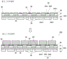
本实施方式的发光基板10的制造方法包括上述的本实施方式的荧光体基板30的制造方法、和将至少一个发光元件20接合于电路图案层34的第五工序(接合工序)。The manufacturing method of light-emitting
〔第一工序〕〔the first process〕
图3A是表示第一工序的开始时及结束时的图。第一工序(电路图案层形成工序的一个例子)是在母板MB(即绝缘层32)的表面31侧形成电路图案层34、在背面33侧形成背面图案层38的工序。本工序例如通过使用了掩模图案(省略图示)的蚀刻而进行。FIG. 3A is a diagram showing the start and end of the first process. The first step (an example of a circuit pattern layer forming step) is a step of forming a
〔第二工序〕〔Second process〕
图3B是表示第二工序的开始时及结束时的图。第二工序(支承层形成工序的一个例子)是在绝缘层32与通过第三工序形成的荧光体层36之间形成支承层35的工序,其中,该支承层35是不包含荧光体的层,且对通过第三工序形成的荧光体层36进行支承。在本工序中,对绝缘层32的表面31中的、除配置有电路图案层34的部分以外的部分涂覆白色涂料(省略图示),来形成支承层35。这里,白色涂料是在构成支承层35的白色颜料(多个白色粒子的集合体)及粘合剂中添加了溶剂的涂料,被涂覆的白色涂料的层在固化后成为支承层35。其结果,若本工序结束,则作为支承层35,形成有包含白色颜料的单层构造的层。另外,在本工序中,以固化后的白色涂料的层的厚度、即支承层35的厚度比电路图案层34的厚度薄的方式涂覆白色涂料。FIG. 3B is a diagram showing the start and end of the second step. The second step (an example of a supporting layer forming step) is a step of forming a supporting
此外,通过本工序形成的支承层35可以在绝缘层32的厚度方向上涂覆一次白色涂料来形成,也可以涂覆多次来形成。In addition, the supporting
〔第三工序〕〔Third process〕
图3C是表示第三工序的开始时及结束时的图。第三工序(荧光体层形成工序的一个例子)是在绝缘层32的表面31侧涂覆荧光体涂料(省略图示)来形成荧光体层36的工序。具体而言,在本工序中,在通过第二工序形成的支承层35的外表面及电路图案层34的外表面涂覆荧光体涂料。即,在本工序中,使荧光体层36的一部分层叠于支承层35。另外,在本工序中,荧光体层36形成于支承层35的外表面及电路图案层34的外表面,但荧光体层36作为一个例子形成为其外表面变得平坦。另外,在本工序中,以荧光体层36中的配置于支承层35的外表面的部分的厚度比支承层35的厚度薄的方式形成荧光体层36。FIG. 3C is a diagram showing the start and end of the third step. The third step (an example of the phosphor layer forming step) is a step of applying phosphor paint (not shown) on the
〔第四工序〕〔Fourth process〕
图3D是表示第四工序的开始时及结束时的图。第四工序是除去荧光体层36的一部分而使电路图案层34的所有接合面34A1露出的工序。这里,在荧光体涂料的粘合剂例如是热固化性树脂的情况下,在通过加热使荧光体涂料固化后使用二维激光加工装置(省略图示)来对荧光体层36中的各接合面34A1上的部分选择性地照射激光。其结果,荧光体层36中的各接合面34A1上的部分被烧蚀,各接合面34A1露出。Fig. 3D is a diagram showing the start and end of the fourth step. The fourth step is a step of removing a part of the
以上的结果,能够制造本实施方式的荧光体基板30。As a result of the above, the
此外,本工序除上述的方法以外,例如也可以通过以下的方法进行。在荧光体涂料的粘合剂例如为UV固化性树脂(感光性树脂)的情况下,对与各接合面34A1重叠的部分(涂料开口部)施加掩模图案,曝光UV光,使该掩模图案以外的部分UV固化,通过树脂除去液除去非曝光部(未固化部),由此使各接合面34A1露出。其后,通常,加热来进行后固化(aftercure)(照相显影法)。另外,也可以代替第三工序及第四工序,而通过使用预先设定有开口部的丝网掩膜(省略图示)的丝网印刷形成荧光体层36(丝网印刷法)。在该情况下,只要预先使丝网掩膜中的与接合面34A1重叠的部分的荧光体涂料开口部堵住即可。In addition, this process can also be performed by the following method other than the above-mentioned method, for example. In the case where the binder of the phosphor paint is, for example, a UV curable resin (photosensitive resin), a mask pattern is applied to the portion (paint opening) overlapping each bonding surface 34A1, and UV light is exposed to make the mask The parts other than the pattern are UV-cured, and the non-exposed parts (uncured parts) are removed by the resin removing liquid, thereby exposing each bonding surface 34A1. Thereafter, generally, heating is performed to perform aftercure (photographic development method). In addition, instead of the third step and the fourth step, the
若本工序结束,则制造出荧光体基板30。After this step is completed,
〔第五工序〕〔fifth process〕
图3E是表示第五工序的开始时及结束时的图。第五工序(接合工序的一个例子)是将多个发光元件20搭载于荧光体基板30的工序。在本工序中,在将荧光体基板30的荧光体层36呈凹状除去而露出的各接合面34A1印刷焊膏SP,在使多个发光元件20的各电极与各接合面34A1对准的状态下熔化焊膏SP。其后,若焊膏SP被冷却固化,则各发光元件20接合于各电极对34A(各接合面34A1)。此外,本工序作为一个例子通过回流工序进行。FIG. 3E is a diagram showing the start and end of the fifth step. The fifth step (an example of the bonding step) is a step of mounting the plurality of
若本工序结束,则制造出发光基板10。When this step is completed, the
以上是对本实施方式的发光基板10的制造方法的说明。The above is the description of the method of manufacturing the light-emitting
<第一实施方式的发光基板的发光动作><Light-Emitting Operation of the Light-Emitting Substrate of the First Embodiment>
接下来,参照图1C以及图4对本实施方式的发光基板10的发光动作进行说明。这里,图4是用于说明本实施方式的发光基板10的发光动作的图。Next, the light-emitting operation of the light-emitting
首先,若使多个发光元件20工作的工作开关(省略图示)接通,则开始从外部电源(省略图示)经由连接器(省略图示)向电路图案层34的供电,从而多个发光元件20将光L呈放射状发散射出,该光L的一部分到达荧光体基板30的表面31A。更具体而言,发光元件20的LED22中的发光在LED22的结电平JL(即PN结面)进行(参照图1C)。First, when an operation switch (not shown) for operating a plurality of
以下,划分射出的光L的行进方向来对光L的动作进行说明。Hereinafter, the behavior of the light L will be described by dividing the traveling direction of the emitted light L. FIG.
从各发光元件20射出的光L的一部分不会射入荧光体层36而向外部射出。在该情况下,光L的波长保持与从各发光元件20射出时的光L的波长相同。Part of the light L emitted from each light emitting
另外,从各发光元件20射出的光L的一部分中的LED22本身的光射入荧光体层36。这里,上述的“光L的一部分中的LED22本身的光”意味着射出的光L中的不被各发光元件20(CSP本身)的荧光体进行颜色转换的光、即LED22本身的光(作为一个例子为蓝色(波长为470nm附近)的光)。而且,若LED22本身的光L与分散在荧光体层36中的荧光体碰撞,则荧光体激励而产生激励光。这里,荧光体激励的理由是因为,分散在荧光体层36中的荧光体使用了对蓝色的光具有激励峰值的荧光体(可见光激励荧光体)。伴随于此,通过光L的能量的一部分使用于荧光体的激励,光L损失一部分能量。其结果,光L的波长被转换(进行波长转换)。例如,根据荧光体层36的荧光体的种类(例如,在荧光体使用了红色系CASN的情况下),光L的波长变长(例如650nm等)。In addition, the light of the
另外,荧光体层36中的激励光保持原样地从荧光体层36射出,但一部分的激励光朝向下侧的电路图案层34,另外,一部分的激励光朝向下侧的支承层35。而且,朝向了电路图案层34的激励光通过电路图案层34中的反射而向外部射出。如以上那样,在荧光体的激励光的波长为600nm以上的情况下,即使电路图案层34为Cu,也能够期待反射效果。此外,根据荧光体层36的荧光体的种类,光L的波长与上述的例子不同,但无论哪种情况,均进行光L的波长转换。例如,在激励光的波长不足600nm的情况下,若将电路图案层34或其表面例如设为Ag(电镀),则能够期待反射效果。相对于此,朝向了支承层35的激励光通过支承层35的白色颜料的反射而向外部射出。在该情况下,能够提高可见光的整个波长区域的反射效果。The excitation light in
如以上那样,各发光元件20射出的光L(各发光元件20呈放射状射出的光L)分别经由上述那样的多个光路与上述激励光一起向外部照射。因此,在荧光体层36所包含的荧光体的发光波长与发光元件20(CSP)中的密封了(或覆盖)LED22的荧光体的发光波长不同的情况下,本实施方式的发光基板10将各发光元件20射出后的光L的束作为包含与各发光元件20射出时的光L的波长不同的波长的光L的光L的束与上述激励光一起照射。例如,本实施方式的发光基板10照射发光元件20射出的光(波长)与从荧光体层36射出的光(波长)的合成光。As described above, the light L emitted from each light emitting element 20 (the light L emitted radially from each light emitting element 20 ) is irradiated to the outside together with the excitation light through the plurality of optical paths as described above. Therefore, when the emission wavelength of the phosphor contained in the
相对于此,在荧光体层36所包含的荧光体的发光波长与发光元件20(CSP)中的密封了(或覆盖)LED22的荧光体的发光波长相同的情况下(相同的相关色温的情况下),本实施方式的发光基板10将各发光元件20射出后的光L的束作为包含与各发光元件20射出后的光L的波长相同的波长的光L的光L的束与上述激励光一起照射。On the other hand, when the emission wavelength of the phosphor contained in the
以上是对本实施方式的发光基板10的发光动作的说明。The above is the description of the light emitting operation of the
<第一实施方式的效果><Effects of the first embodiment>
接下来,参照附图对本实施方式的效果进行说明。Next, effects of the present embodiment will be described with reference to the drawings.
〔第一效果〕[first effect]
关于第一效果,将本实施方式与以下说明的比较方式(参照图5)进行比较来说明。这里,在比较方式的说明中,在使用与本实施方式相同的构成要素等的情况下,对该构成要素等使用与本实施方式的情况相同的名称、附图标记等。图5是用于对比较方式的发光基板10a的发光动作进行说明的图。比较方式的发光基板10a(搭载多个发光元件20的基板30a)除不具备荧光体层36的方面以外,为与本实施方式的发光基板10(荧光体基板30)相同的结构。Regarding the first effect, the present embodiment will be described in comparison with a comparative form (see FIG. 5 ) described below. Here, in the description of the comparative form, when the same components and the like as in the present embodiment are used, the same names, reference numerals and the like as in the present embodiment are used for the components and the like. FIG. 5 is a diagram for explaining the light-emitting operation of the light-emitting substrate 10 a of the comparative embodiment. The light-emitting substrate 10a (substrate 30a on which a plurality of light-emitting
在比较方式的发光基板10a的情况下,从各发光元件20射出并射入到基板30a的表面31A的光L不被转换波长而进行反射或散射。因此,在比较方式的基板30a的情况下,在搭载了发光元件20的情况下无法调整为与发光元件20发出的光不同的发光颜色的光。即,在比较方式的发光基板10a的情况下,无法调整为与发光元件20发出的光不同的发光颜色的光。In the case of the light-emitting substrate 10 a of the comparative embodiment, the light L emitted from each light-emitting
相对于此,在本实施方式的情况下,从绝缘层32的厚度方向观察,在绝缘层32的表面31的与各发光元件20的各接合面34A1的周围配置有荧光体层36。因此,从各发光元件20呈放射状射出的光L的一部分射入荧光体层36,并被荧光体层36进行波长转换,而向外部照射。在该情况下,从各发光元件20呈放射状射出的光L的一部分射入荧光体层36,使荧光体层36所包含的荧光体激励,产生激励光。On the other hand, in the present embodiment,
因此,根据本实施方式的荧光体基板30,在搭载了发光元件20的情况下,能够将从荧光体基板30发出的光L调整为与发光元件20发出的光L不同的发光颜色的光。伴随于此,根据本实施方式的发光基板10,能够将从荧光体基板30发出的光L调整为与发光元件20发出的光L不同的发光颜色的光L。若从另一个角度来看,根据本实施方式的发光基板10,能够将与发光元件20发出的光L不同的发光颜色的光L向外部照射。Therefore, according to the
〔第二效果〕[second effect]
关于第二效果,将本实施方式与比较方式(参照图5)比较来进行说明。在比较方式的情况下,如图5所示,因各发光元件20的配置间隔而在向外部照射的光L中产生光斑。这里,光L的光斑越大,炫光越大。Regarding the second effect, the present embodiment will be described in comparison with the comparative form (see FIG. 5 ). In the case of the comparative system, as shown in FIG. 5 , flare occurs in the light L irradiated to the outside due to the arrangement intervals of the respective
相对于此,在本实施方式的荧光体基板30的表面31A侧,如图2B所示,在除各接合面34A1以外的部分整体上设置有荧光体层36。因此,在本实施方式的发光基板10中,从各接合面34A1的周围(各发光元件20的周围)也产生激励光。On the other hand, on the
因此,根据本实施方式,与比较方式相比,能够减小炫光。Therefore, according to the present embodiment, it is possible to reduce glare compared to the comparative method.
此外,本效果在遍及绝缘层32的整个面设置有荧光体层36的情况下,具体而言,从表面31侧观察,在荧光体层36相对于绝缘层32的表面31所占的比例为表面31的80%以上的情况下更加有效。In addition, in the case where the
〔第三效果〕[Third effect]
在本实施方式的情况下,荧光体层36的一部分被支承层35支承(参照图1C及图3E)。这里,由于构成支承层35的白色颜料比构成荧光体层36的荧光体价格低廉,因此用于形成支承层35的白色涂料也比荧光体涂料价格低廉。In the case of this embodiment, a part of
因此,与支承层35由荧光体层36形成的情况相比,本实施方式的荧光体基板30价格低廉。伴随于此,本实施方式的荧光体基板30的制造方法与由荧光体层36形成支承层35的荧光体基板的制造方法相比,荧光体基板30的制造成本价格低廉。Therefore, the
此外,在本实施方式的发光基板10的情况下,考虑多个LED22的发光时的发热及进行激励的荧光体层36的发热的影响,例如,将电路图案层34的厚度设定为比通常的电路基板厚(作为一个例子为175μm)。在此基础上,在本实施方式的情况下,将荧光体层36的外表面设定在比电路图案层34的外表面靠绝缘层32的厚度方向的外侧。本效果在本实施方式那样的以上的结构的情况下变得显著。In addition, in the case of the light-emitting
〔第四效果〕[Fourth effect]
另外,在本实施方式的情况下,如上述那样,荧光体层36的厚度比支承层35的厚度薄。In addition, in the case of the present embodiment, the thickness of the
因此,本实施方式的荧光体基板30与荧光体层36的厚度为支承层35的厚度以下的情况相比价格低廉。伴随于此,本实施方式的荧光体基板30的制造方法与荧光体层36的厚度为支承层35的厚度以下的荧光体基板的制造方法相比,荧光体基板30的制造成本价格低廉。Therefore, the
〔第五效果〕[fifth effect]
在本实施方式的情况下,如上述那样,支承层35包含白色颜料。因此,根据本实施方式,能够提高形成可见光的激励光的整个波长区域的反射效果。In the case of the present embodiment, the supporting
〔第六效果〕[Sixth effect]
在本实施方式的情况下,D150与D250具有下述的(式1)的关系。In the case of the present embodiment, D1 50 and D2 50 have the following relationship (Formula 1).
(式1)0.8≤D250/D150≤1.2(Formula 1) 0.8≤D2 50 /D1 50 ≤1.2
通过以上的结构,各层的微粒(多个荧光体粒子及多个白色粒子)的中值直径的差被设定为比较小。With the above structure, the difference in the median diameter of the fine particles (a plurality of phosphor particles and a plurality of white particles) in each layer is set to be relatively small.
因此,对于本实施方式的荧光体基板30而言,支承层35与荧光体层36的热膨胀系数(CTE)的差变小的结果,能够减少它们的界面产生的应力。Therefore, in the
以上是对本实施方式的效果的说明。The above is the description of the effect of this embodiment.
另外,以上是对第一实施方式的说明。In addition, the above is the description of the first embodiment.
《第二实施方式》"Second Embodiment"
接下来,参照图6及图7A~图7D对第二实施方式进行说明。以下,仅对本实施方式中的与第一实施方式(参照图1C、图3A~图3E等)不同的部分进行说明。Next, a second embodiment will be described with reference to FIG. 6 and FIGS. 7A to 7D . Hereinafter, only the portions of the present embodiment that are different from the first embodiment (see FIG. 1C , FIGS. 3A to 3E , etc.) will be described.
<第二实施方式的结构><Structure of the second embodiment>
本实施方式的荧光体基板30A(参照图6)相对于第一实施方式的荧光体基板30(参照图1C),在支承层35也配置于电路图案层34的非接合面34B1的方面上不同。此外,支承层35形成于绝缘层32的表面31的一部分及电路图案层34的非接合面34B1,但其外表面是平坦的。
<第二实施方式的荧光体基板的制造方法><Manufacturing method of phosphor substrate according to the second embodiment>
接下来,参照图7A~图7D对本实施方式的荧光体基板30A的制造方法进行说明。本实施方式的发光基板10A的制造方法包括第一工序、第二工序、第三工序、第四工序及第五工序,各工序按它们的记载顺序进行。Next, a method of manufacturing the
〔第一工序〕〔the first process〕
本工序与第一实施方式的情况相同(引用图3A)。This step is the same as that of the first embodiment (see FIG. 3A ).
〔第二工序〕〔Second process〕
图7A是表示第二工序的开始时及结束时的图。第二工序(支承层形成工序的一个例子)是在绝缘层32与通过第三工序形成的荧光体层36之间形成支承层35的工序,其中,该支承层35是不包含荧光体的层,且对通过第三工序形成的荧光体层36进行支承。在本工序中,对绝缘层32的表面31中的、除配置有电路图案层34的部分以外的部分及电路图案层34的整个外表面区域涂覆白色涂料(省略图示,与第一实施方式的情况相同),以外表面在整个区域变得平坦的方式形成支承层35。若本工序结束,则作为支承层35,形成包含白色颜料的单层构造的层。FIG. 7A is a diagram showing the start and end of the second process. The second step (an example of a supporting layer forming step) is a step of forming a supporting
〔第三工序〕〔Third process〕
图7B是表示第三工序的开始时及结束时的图。第三工序(荧光体层形成工序的一个例子)是在绝缘层32的表面31侧涂覆荧光体涂料(省略图示)来形成荧光体层36的工序。具体而言,在本工序中,在通过第二工序形成的支承层35的外表面涂覆荧光体涂料。FIG. 7B is a diagram showing the start and end of the third step. The third step (an example of the phosphor layer forming step) is a step of applying phosphor paint (not shown) on the
〔第四工序〕〔Fourth process〕
图7C是表示第四工序的开始时及结束时的图。第四工序是除去荧光体层36的一部分及支承层35的一部分而使电路图案层34的所有接合面34A1露出的工序。使接合面34A1露出的工序在与第一实施方式相同的工序中,适当地选择通过激光照射而除去的方法、照相印刷法、丝网印刷法等方法来进行。若本工序结束,则制造出荧光体基板30A。FIG. 7C is a diagram showing the start and end of the fourth step. The fourth step is a step of removing a part of the
〔第五工序〕〔fifth process〕
图7D是表示第五工序的开始时及结束时的图。第五工序(接合工序的一个例子)是将多个发光元件20搭载于荧光体基板30的工序。该工序与通过第一实施方式的图3E进行了说明的工序同样地,通过回流处理,将焊膏SP印刷于各接合面34A1并将多个发光元件20搭载于各接合面34A1来进行接合。若本工序结束,则制造出发光基板10A。Fig. 7D is a diagram showing the start and end of the fifth step. The fifth step (an example of the bonding step) is a step of mounting the plurality of
以上是对本实施方式的发光基板10A的制造方法的说明。The above is the description of the method of manufacturing the
<第二实施方式的发光基板的发光动作><Light-Emitting Operation of the Light-Emitting Substrate of the Second Embodiment>
接下来,对本实施方式的发光基板10A的发光动作进行说明。本实施方式的发光基板10A的发光动作基本上与第一实施方式的情况相同。然而,本实施方式的发光基板10A与第一实施方式的情况不同,电路图案层34中的非接合面34B1被支承层35覆盖。因此,荧光体层36中的激励光中的朝向了电路图案层34的激励光被支承层35反射。Next, the light emitting operation of the
以上是对本实施方式的发光基板10A的发光动作的说明。The above is the description of the light emitting operation of the
<第二实施方式的效果><Effect of the second embodiment>
在本实施方式的情况下,与第一实施方式的情况不同,荧光体层36的整个区域被包含白色颜料的支承层35支承。因此,根据本实施方式,能够在荧光体层36的整个区域,提高形成可见光的激励光的全部波长区域的反射效果。In the case of the present embodiment, unlike the case of the first embodiment, the entire area of the
本实施方式的其他效果与第一实施方式的情况相同。Other effects of this embodiment are the same as those of the first embodiment.
以上是对本实施方式的效果的说明。The above is the description of the effect of this embodiment.
另外,以上是对第二实施方式的说明。In addition, the above is the description of the second embodiment.
《第三实施方式》"Third Embodiment"
接下来,参照图8及图9A~图9E对第三实施方式进行说明。以下,仅对本实施方式中的与第二实施方式(参照图6等)不同的部分进行说明。Next, a third embodiment will be described with reference to FIG. 8 and FIGS. 9A to 9E . Hereinafter, only the differences between this embodiment and the second embodiment (see FIG. 6 and the like) will be described.
<第三实施方式的结构><Structure of the third embodiment>
本实施方式的荧光体基板30B(参照图8)相对于第二实施方式的荧光体基板30A(参照图6),在支承层35B为多层构造的方面上不同。具体而言,本实施方式的支承层35B由第一层35B1(基层的一个例子)和第二层35B2(邻接层的一个例子)构成。第一层35B1配置于绝缘层32的表面31中的除形成有电路图案层34的部分以外的部分。而且,第一层35B1的厚度比电路图案层34的厚度薄。第二层35B2配置于第一层35B1及电路图案层34的非接合面34B1。这里,第一层35B1是不包含白色颜料的层,作为一个例子是从第一实施方式及第二实施方式的支承层35中去除了白色颜料的层。另外,第二层35B2的一部分配置在第一层35B1与荧光体层36之间,剩余的一部分配置在电路图案层34与荧光体层36之间。即,第二层35B2为与荧光体层36邻接的层。第二层35B2是包含白色颜料的层,作为一个例子为与第一实施方式及第二实施方式的支承层35相同的材质。第二层35B2的厚度作为一个例子比第一层35B1的厚度薄。根据以上的结构,第一层35B1配置在绝缘层32与第二层35B2之间。另外,本实施方式的支承层35B的厚度作为一个例子比荧光体层36的厚度薄。A
<第三实施方式的荧光体基板的制造方法><Method of Manufacturing Phosphor Substrate of Third Embodiment>
接下来,参照图9A~图9E对本实施方式的荧光体基板30B的制造方法进行说明。本实施方式的发光基板10B的制造方法包括第一工序、第二工序、第三工序、第四工序及第五工序,各工序按它们的记载顺序进行。Next, a method of manufacturing the
〔第一工序〕〔the first process〕
本工序与第一实施方式的情况相同(引用图3A)。This step is the same as that of the first embodiment (see FIG. 3A ).
〔第二工序〕〔Second process〕
图9A是表示第二工序的开始时及前半部分的结束时的图,图9B是表示第二工序的前半部分的结束时(后半部分的开始时)及后半部分的结束时(结束时)的图。第二工序(支承层形成工序的一个例子)是在绝缘层32与通过第三工序形成的荧光体层36之间形成支承层35B(第一层35B1及第二层35B2)的工序。即,本工序(支承层形成工序的一个例子)是在绝缘层32形成支承层35B的工序,其中,该支承层35B是不包含荧光体的层,且对通过第三工序形成的荧光体层36进行支承。本工序被分为图9A所示的前半部分的工序、和图9B所示的后半部分的工序。9A is a diagram showing the beginning of the second process and the end of the first half, and FIG. 9B is a diagram showing the end of the first half of the second process (the beginning of the second half) and the end of the second half (the end of the second half). ) graph. The second step (an example of the supporting layer forming step) is a step of forming supporting
在前半部分的工序中,对绝缘层32的表面31中的、除配置有电路图案层34的部分以外的部分涂覆成为第一层35B1的基础的涂料(省略图示),形成第一层35B1(参照图9A)。In the first half of the process, a paint (not shown) serving as a basis for the first layer 35B1 is applied to the portion of the
接下来,在后半部分的工序中,对通过前半部分的工序形成的第一层35B1及电路图案层34的非接合面34B1的整个外表面区域涂覆成为第二层35B2的基础的白色涂料(省略图示,与第一实施方式的情况相同),形成外表面在整个区域平坦的第二层35B2(参照图9B)。Next, in the second half of the process, the first layer 35B1 formed in the first half of the process and the entire outer surface area of the non-joint surface 34B1 of the
然后,若本工序结束,则在绝缘层32的表面31中的、除配置有电路图案层34的部分以外的部分,形成作为多层构造的支承层35B(第一层35B1及第二层35B2)。Then, when this process ends, in the
〔第三工序〕〔Third process〕
图9C是表示第三工序的开始时及结束时的图。第三工序(荧光体层形成工序的一个例子)是在绝缘层32的表面31侧涂覆荧光体涂料(省略图示)来形成荧光体层36的工序。具体而言,在本工序中,在通过第二工序形成的支承层35B的外表面(第二层35B2的外表面)涂覆荧光体涂料(省略图示)。FIG. 9C is a diagram showing the start and end of the third step. The third step (an example of the phosphor layer forming step) is a step of applying phosphor paint (not shown) on the
〔第四工序〕〔Fourth process〕
图9D是表示第四工序的开始时及结束时的图。第四工序是除去荧光体层36的一部分及支承层35B的一部分而使电路图案层34的所有接合面34A1露出的工序。使接合面34A1露出的工序在与第一、第二实施方式相同的工序中,适当地选择通过激光照射而除去的方法、照相印刷法、丝网印刷法等方法来进行。若本工序结束,则制造出荧光体基板30B。FIG. 9D is a diagram showing the start and end of the fourth step. The fourth step is a step of removing a part of the
〔第五工序〕〔fifth process〕
图9E是表示第五工序的开始时及结束时的图。第五工序(接合工序的一个例子)是将多个发光元件20搭载于荧光体基板30B的工序。该工序与通过第一及第二实施方式的图3E、图7D进行了说明的工序同样地,通过回流处理,将焊膏SP印刷于各接合面34A1并将多个发光元件20搭载于各接合面34A1来进行接合。FIG. 9E is a diagram showing the start and end of the fifth step. The fifth step (an example of a bonding step) is a step of mounting the plurality of
若本工序结束,则制造出发光基板10B。When this step is completed, the
以上是对本实施方式的发光基板10B的制造方法的说明。The above is the description of the method of manufacturing the
<第三实施方式的发光基板的发光动作><Light-emitting operation of the light-emitting substrate according to the third embodiment>
本实施方式的发光基板10B的发光动作基本上与第二实施方式的情况相同。The light emitting operation of the
以上是对本实施方式的发光基板10B的发光动作的说明。The above is the description of the light emitting operation of the
<第三实施方式的效果><Effect of the third embodiment>
本实施方式的荧光体基板30B与第二实施方式的荧光体基板30A(参照图6)同样地,荧光体层36的整个区域被包含白色颜料的支承层35B支承。具体而言,荧光体层36配置在构成支承层35B的第二层35B2上。因此,根据本实施方式,能够在荧光体层36的整个区域,提高形成可见光的激励光的全部波长区域的反射效果。Like the
另外,本实施方式的荧光体基板30B与第二实施方式的荧光体基板30A(参照图6)不同,支承层35B的下侧的部分由不包含白色颜料的第一层35B1构成。因此,与第二实施方式的荧光体基板30A相比,本实施方式的荧光体基板30B价格低廉。In addition, the
本实施方式的其他效果与第一实施方式及第二实施方式的情况相同。Other effects of this embodiment are the same as those of the first and second embodiments.
以上是对本实施方式的效果的说明。The above is the description of the effect of this embodiment.
以上是对第三实施方式的说明。The above completes the description of the third embodiment.
《第四实施方式》"Fourth Embodiment"
接下来,参照图10及图11A~图11E对第四实施方式进行说明。以下,仅对本实施方式中的与第二实施方式(参照图6等)不同的部分进行说明。Next, a fourth embodiment will be described with reference to FIG. 10 and FIGS. 11A to 11E . Hereinafter, only the differences between this embodiment and the second embodiment (see FIG. 6 and the like) will be described.
<第四实施方式的结构><Structure of the fourth embodiment>
本实施方式的荧光体基板30C(参照图10)与第二实施方式的荧光体基板30A(参照图6)不同,电路图案层34的接合面34A1位于比非接合面34A2靠绝缘层32的厚度方向外侧的位置。换句话说,本实施方式的情况与第二实施方式的情况不同,各电极对34A比配线部分34B向绝缘层32的厚度方向外侧突出。The
<第四实施方式的荧光体基板的制造方法><Method of Manufacturing Phosphor Substrate of Fourth Embodiment>
接下来,参照图11A~图11E对本实施方式的荧光体基板30C的制造方法进行说明。本实施方式的发光基板10C的制造方法包括第一工序、第二工序、第三工序、第四工序及第五工序,各工序按它们的记载顺序进行。Next, a method of manufacturing the
〔第一工序〕〔the first process〕
图11A是表示第一工序的开始时及结束时的图。第一工序是在母板MB的表面31A侧形成电路图案层34、在背面33A侧形成背面图案层38的工序。FIG. 11A is a diagram showing the start and end of the first process. The first step is a step of forming the
此外,在通过本工序形成电路图案层34的情况下,首先在母板MB的表面31A侧通过例如使用了掩模图案(省略图示)的蚀刻形成从厚度方向观察与电路图案层34相同的形状的图案。接下来,例如通过使用了掩模图案(省略图示)的蚀刻对该图案的一部分(相当于配线部分34B的部分)进行半阴影(蚀刻至厚度方向的中途)。In addition, in the case of forming the
〔第二工序〕〔Second process〕
图11B是表示第二工序的开始时及前半部分的结束时的图。第二工序(支承层形成工序的一个例子)是在绝缘层32与通过第三工序形成的荧光体层36之间形成支承层35C的工序。在本工序中,对绝缘层32的表面31中的、除配置有电路图案层34的部分以外的部分及电路图案层34的非接合面34B1的整个外表面区域涂覆白色涂料(省略图示,与第一实施方式的情况相同),形成支承层35C。在该情况下,在本工序中,在所有电极对34A比支承层35C的外表面突出的状态下,使支承层35C的外表面在整个区域变得平坦。若本工序结束,则作为支承层35C,形成包含白色颜料的单层构造的层。FIG. 11B is a diagram showing the start of the second process and the end of the first half. The second step (an example of a supporting layer forming step) is a step of forming a supporting
〔第三工序〕〔Third process〕
图11C是表示第三工序的开始时及结束时的图。第三工序(荧光体层形成工序的一个例子)是在绝缘层32的表面31侧涂覆荧光体涂料(省略图示)来形成荧光体层36的工序。具体而言,在本工序中,在通过第二工序形成的支承层35C的外表面涂覆荧光体涂料(省略图示)。在该情况下,在本工序中,以所有电极对34A被荧光体层36覆盖的方式形成荧光体层36。FIG. 11C is a diagram showing the start and end of the third step. The third step (an example of the phosphor layer forming step) is a step of applying phosphor paint (not shown) on the
〔第四工序〕〔Fourth process〕
图11D是表示第四工序的开始时及结束时的图。第四工序是除去荧光体层36的一部分而使电路图案层34的所有接合面34A1露出的工序。使接合面34A1露出的工序在与第一~第三实施方式相同的工序中,适当地选择通过激光照射而除去的方法、照相印刷法、丝网印刷法等方法来进行。FIG. 11D is a diagram showing the start and end of the fourth step. The fourth step is a step of removing a part of the
若本工序结束,则制造出荧光体基板30C。When this step is completed, the
〔第五工序〕〔fifth process〕
图11E是表示第五工序的开始时及结束时的图。第五工序(接合工序的一个例子)是将多个发光元件20搭载于荧光体基板30C的工序。该工序与通过第一~第三实施方式的图3E、图7D、图9E进行了说明的工序同样地,通过回流处理,将焊膏SP印刷于各接合面34A1并将多个发光元件20搭载于各接合面34A1来进行接合。若本工序结束,则制造出发光基板10C。FIG. 11E is a diagram showing the start and end of the fifth step. The fifth step (an example of a bonding step) is a step of mounting a plurality of
以上是对本实施方式的发光基板10C的制造方法的说明。The above is the description of the method of manufacturing the
<第四实施方式的发光基板的发光动作><Light-Emitting Operation of the Light-Emitting Substrate of the Fourth Embodiment>
本实施方式的发光基板10C的发光动作基本上与第二实施方式的情况相同。The light emitting operation of the
以上是对本实施方式的发光基板10C的发光动作的说明。The above is the description of the light emitting operation of the
<第四实施方式的效果><Effect of the fourth embodiment>
本实施方式的效果与第一实施方式、第二实施方式及第三实施方式的情况相同。The effects of this embodiment are the same as those of the first embodiment, the second embodiment, and the third embodiment.
以上是对本实施方式的效果的说明。The above is the description of the effect of this embodiment.
以上是对第四实施方式的说明。This concludes the description of the fourth embodiment.
《第五实施方式》"Fifth Embodiment"
接下来,参照图12及图13A~图13E对第五实施方式进行说明。以下,仅对本实施方式中的与第四实施方式(参照图10等)不同的部分进行说明。Next, a fifth embodiment will be described with reference to FIG. 12 and FIGS. 13A to 13E . Hereinafter, only the differences between this embodiment and the fourth embodiment (see FIG. 10 and the like) will be described.
<第五实施方式的结构><Structure of Fifth Embodiment>
本实施方式的荧光体基板30D(参照图12)与第四实施方式的荧光体基板30C(参照图10)不同,在支承层35D为多层构造的方面上不同。具体而言,本实施方式的支承层35D由第一层35D1(基层的一个例子)和第二层35D2(邻接层的一个例子)构成。第一层35D1配置于绝缘层32的表面31中的除形成有电路图案层34的部分以外的部分。而且,第一层35D1的厚度比电路图案层34的厚度薄。第二层35D2配置于第一层35D1及电路图案层34的非接合面34B1。这里,第一层35D1是不包含白色颜料的层,作为一个例子是与第三实施方式的第一层35B1相同的层。另外,第二层35D2的一部分配置在第一层35D1与荧光体层36之间,剩余的一部分配置在电路图案层34与荧光体层36之间。即,第二层35D2为与荧光体层36邻接的层。第二层35D2是包含白色颜料的层,作为一个例子为与第三实施方式的第二层35B2相同的材质。第二层35D2的厚度作为一个例子比第一层35D1的厚度薄。根据以上的结构,第一层35D1配置在绝缘层32与第二层35D2之间。另外,本实施方式的支承层35D的厚度作为一个例子比荧光体层36的厚度薄。A
<第五实施方式的荧光体基板的制造方法><Manufacturing method of phosphor substrate according to fifth embodiment>
接下来,参照图13A~图13E对本实施方式的荧光体基板30D的制造方法进行说明。本实施方式的发光基板10D的制造方法包括第一工序、第二工序、第三工序、第四工序及第五工序,各工序按它们的记载顺序进行。Next, a method of manufacturing the
〔第一工序〕〔the first process〕
本工序与第四实施方式的情况相同(引用图11A)。This step is the same as that of the fourth embodiment (see FIG. 11A ).
〔第二工序〕〔Second process〕
图13A是表示第二工序的开始时及前半部分的结束时的图,图13B是表示第二工序的前半部分的结束时(后半部分的开始时)及后半部分的结束时(结束时)的图。第二工序(支承层形成工序的一个例子)是在绝缘层32与通过第三工序形成的荧光体层36之间形成支承层35D的工序。即,本工序是在绝缘层32形成支承层35D的工序,其中,该支承层35D是不包含荧光体的层,且对通过第三工序形成的荧光体层36进行支承。本工序被分为图13A所示的前半部分的工序、和图13B所示的后半部分的工序。13A is a diagram showing the beginning of the second process and the end of the first half, and FIG. 13B is a diagram showing the end of the first half of the second process (the start of the second half) and the end of the second half (the end of the second half). ) graph. The second step (an example of a supporting layer forming step) is a step of forming a supporting
在前半部分的工序中,对绝缘层32的表面31中的、除配置有电路图案层34的部分以外的部分涂覆成为第一层35D1的基础的涂料(省略图示),形成第一层35D1(参照图13A)。In the first half of the process, a paint (not shown) serving as a basis for the first layer 35D1 is applied to the portion of the
接下来,在后半部分的工序中,对通过前半部分的工序形成的第一层35D1及电路图案层34的非接合面34B1的整个外表面区域涂覆成为第二层35D2的基础的白色涂料(省略图示,与第一实施方式的情况相同),形成第二层35D2(参照图13B)。在该情况下,在本工序中,在所有电极对34A比第一层35D1的外表面从绝缘层32的外表面突出的状态下,使支承层35D的外表面在整个区域变得平坦。若本工序结束,则形成多层构造的支承层35D。Next, in the latter half of the process, the first layer 35D1 formed in the first half of the process and the entire outer surface area of the non-joint surface 34B1 of the
〔第三工序〕〔Third process〕
图13C是表示第三工序的开始时及结束时的图。第三工序(荧光体层形成工序的一个例子)是在绝缘层32的表面31侧涂覆荧光体涂料(省略图示)来形成荧光体层36的工序。本工序基本上以与第四实施方式的情况相同的方式进行。Fig. 13C is a diagram showing the start and end of the third step. The third step (an example of the phosphor layer forming step) is a step of applying phosphor paint (not shown) on the
〔第四工序〕〔Fourth process〕
图13D是表示第四工序的开始时及结束时的图。第四工序是除去荧光体层36的一部分而使电路图案层34的所有接合面34A1露出的工序。使接合面34A1露出的工序在与第一~第四实施方式相同的工序中,适当地选择通过激光照射而除去的方法、照相印刷法、丝网印刷法等方法来进行。Fig. 13D is a diagram showing the start and end of the fourth step. The fourth step is a step of removing a part of the
若本工序结束,则制造出荧光体基板30D。When this step is completed, the
〔第五工序〕〔fifth process〕
图13E是表示第五工序的开始时及结束时的图。第五工序(接合工序的一个例子)是将多个发光元件20搭载于荧光体基板30D的工序。该工序与通过第一~第四实施方式的图3E、图7D、图9E、图11E进行了说明的工序同样地,通过回流处理,将焊膏SP印刷于各接合面34A1并将多个发光元件20搭载于各接合面34A1来进行接合。FIG. 13E is a diagram showing the start and end of the fifth step. The fifth step (an example of a bonding step) is a step of mounting a plurality of
若本工序结束,则制造出发光基板10D。When this step is completed, the
以上是对本实施方式的发光基板10D的制造方法的说明。The above is the description of the method of manufacturing the
<第五实施方式的发光基板的发光动作><Light-emitting operation of the light-emitting substrate according to the fifth embodiment>
本实施方式的发光基板10D的发光动作基本上与第二实施方式的情况相同。The light emitting operation of the
以上是对本实施方式的发光基板10D的发光动作的说明。The above is the description of the light emitting operation of the
<第五实施方式的效果><Effects of the fifth embodiment>
本实施方式的荧光体基板30D与第四实施方式的荧光体基板30C(参照图10)不同,支承层35D的下侧的部分由不包含白色颜料的第一层35D1构成。因此,与第四实施方式的荧光体基板30C相比,本实施方式的荧光体基板30D价格低廉。The
本实施方式的其他效果与第一实施方式、第二实施方式、第三实施方式及第四实施方式的情况相同。Other effects of this embodiment are the same as those of the first, second, third, and fourth embodiments.
以上是对本实施方式的效果的说明。The above is the description of the effect of this embodiment.
以上是对第五实施方式的说明。This concludes the description of the fifth embodiment.
如以上那样,针对本发明以上述的各实施方式为例进行了说明,但本发明并不限定于上述的各实施方式。在本发明的技术范围内例如还包含下述那样的方式(变形例)。As above, the present invention has been described by taking the above-mentioned embodiments as examples, but the present invention is not limited to the above-mentioned embodiments. For example, the following aspects (modified examples) are also included in the technical scope of the present invention.
例如,在各实施方式的说明中,将发光元件20的一个例子设为CSP。然而,发光元件20的一个例子也可以是CSP以外的发光元件。例如,也可以是仅搭载了倒装芯片的发光元件。另外,也能够应用于COB设备的基板本身。For example, in the description of each embodiment, an example of the
另外,在各实施方式的说明中,在荧光体基板30搭载多个发光元件20,发光基板10具备多个发光元件20。然而,若考虑上述的第一效果的说明的机理,则可知即使发光元件20为一个,也起到第一效果。因此,搭载于荧光体基板30的发光元件20的数量只要至少为一个即可。另外,搭载于发光基板10的发光元件20只要至少为一个即可。In addition, in the description of each embodiment, the plurality of
另外,在各实施方式的说明中,荧光体层36中的绝缘层32的厚度方向外侧的面位于比电路图案层34靠该厚度方向外侧的位置(参照图1C、图3D等)。然而,若考虑上述的第一效果的说明的机理,则荧光体层36中的绝缘层32的厚度方向外侧的面也可以为与电路图案层34的接合面34A1在该厚度方向相同的位置或者比接合面34A1靠该厚度方向内侧的位置。In the description of each embodiment, the outer surface of the insulating
另外,在各实施方式的说明中,在荧光体基板30的背面33A侧具备背面图案层38(参照图1B)。然而,若考虑上述的第一效果的说明的机理,则也可以在荧光体基板30的背面33A侧不具备背面图案层38。In addition, in the description of each embodiment, the back
另外,在本实施方式的说明中,荧光体层36配置于绝缘层32及电路图案层34的表面31A侧的、除多个电极对34A以外的部分(参照图2B)。然而,荧光体层36也可以不遍及荧光体基板30的表面31A侧的除多个电极对34A以外的部分的整个区域配置。In addition, in the description of the present embodiment, the
另外,在各实施方式的说明中,在制造荧光体基板30及发光基板10时,说明了将利昌工业株式会社制的CS-3305A作为母板MB来使用。然而,这为一个例子,也可以使用不同的母板MB。例如,不拘泥于利昌工业株式会社制的CS-3305A的绝缘层厚、铜箔厚等的标准规格,也可以特别使用铜箔厚更厚的母板。In addition, in the description of each embodiment, it has been described that CS-3305A manufactured by Richang Industry Co., Ltd. is used as the mother board MB when manufacturing the
此外,各实施方式的发光基板10(也包含其变形例)能够与其他构成要素组合来应用于照明装置。这种情况下的其他构成要素为供给用于使发光基板10的发光元件20发光的电力的电源等。In addition, the light-emitting substrate 10 (including its modification) of each embodiment can be applied to a lighting device in combination with other components. Another component in this case is a power supply for supplying electric power for causing the
另外,在第三实施方式中,支承层35B作为多层构造说明了由第一层35B1及第二层35B2构成的双层构造。然而,只要支承层35B包括包含白色颜料的层,则作为多层构造的支承层35B也可以是3层构造以上的构造。关于这一方面,第五实施方式的情况也相同。In addition, in the third embodiment, the
本申请主张以2020年8月28日申请的日本申请特愿2020-144279号为基础的优先权,将其公开的全部内容引入到这里。This application claims priority based on Japanese Application Japanese Patent Application No. 2020-144279 filed on August 28, 2020, and the entire disclosure thereof is incorporated here.
附图标记说明Explanation of reference signs
10、10A、10B、10C、10D…发光基板;20…发光元件;22…LED;30、30A、30B、30C、30D…荧光体基板;32…绝缘层(绝缘基板的一个例子);34…电路图案层;34A…电极对;34A1…接合面;34A2…非接合面;34B…配线部分;34B1…非接合面;35、30B、30C、30D…支承层;35B1、30D1…第一层;35B2、30D2…第二层;36…荧光体层;37…端子;38…背面图案层;39…贯通孔;L…光;MB…母板;SP…焊膏。10, 10A, 10B, 10C, 10D...Light-emitting substrate; 20...Light-emitting element; 22...LED; 30, 30A, 30B, 30C, 30D...Phosphor substrate; 32...Insulating layer (an example of insulating substrate); 34... Circuit pattern layer; 34A...electrode pair; 34A1...joining surface; 34A2...non-joining surface; 34B...wiring part; 34B1...non-joining surface; 35, 30B, 30C, 30D...supporting layer; ; 35B2, 30D2...second layer; 36...phosphor layer; 37...terminal; 38...back pattern layer; 39...through hole; L...light; MB...motherboard; SP...solder paste.
Claims (12)
Applications Claiming Priority (3)
| Application Number | Priority Date | Filing Date | Title |
|---|---|---|---|
| JP2020-144279 | 2020-08-28 | ||
| JP2020144279 | 2020-08-28 | ||
| PCT/JP2021/030626 WO2022045013A1 (en) | 2020-08-28 | 2021-08-20 | Phosphor substrate, light-emitting substrate, and lighting device |
Publications (1)
| Publication Number | Publication Date |
|---|---|
| CN115989591A true CN115989591A (en) | 2023-04-18 |
Family
ID=80355173
Family Applications (1)
| Application Number | Title | Priority Date | Filing Date |
|---|---|---|---|
| CN202180053059.5A Withdrawn CN115989591A (en) | 2020-08-28 | 2021-08-20 | Phosphor substrate, light emitting substrate and lighting device |
Country Status (6)
| Country | Link |
|---|---|
| US (1) | US20230335685A1 (en) |
| JP (1) | JP7523550B2 (en) |
| KR (1) | KR20230054838A (en) |
| CN (1) | CN115989591A (en) |
| TW (1) | TW202215678A (en) |
| WO (1) | WO2022045013A1 (en) |
Family Cites Families (18)
| Publication number | Priority date | Publication date | Assignee | Title |
|---|---|---|---|---|
| JP2599649B2 (en) * | 1991-03-26 | 1997-04-09 | 日本無線株式会社 | Resin sealing mounting method for electronic components |
| JP2005159045A (en) | 2003-11-26 | 2005-06-16 | Sumitomo Electric Ind Ltd | Semiconductor light emitting element mounting member and light emitting diode using the same |
| JP2009151290A (en) * | 2007-11-30 | 2009-07-09 | Konica Minolta Business Technologies Inc | White particle |
| JP2009267289A (en) * | 2008-04-30 | 2009-11-12 | Citizen Electronics Co Ltd | Light-emitting device |
| US8110839B2 (en) * | 2009-07-13 | 2012-02-07 | Luxingtek, Ltd. | Lighting device, display, and method for manufacturing the same |
| JP2011228673A (en) * | 2010-03-30 | 2011-11-10 | Mitsubishi Chemicals Corp | Light emitting device |
| JP2012015254A (en) | 2010-06-30 | 2012-01-19 | Nitto Denko Corp | Phosphor ceramic and light emitting device |
| JP5720454B2 (en) * | 2010-07-26 | 2015-05-20 | 旭硝子株式会社 | Light-emitting element mounting substrate, method for manufacturing the same, and light-emitting device |
| US9458379B2 (en) * | 2012-05-31 | 2016-10-04 | National Institute For Materials Science | Phosphor, method for manufacturing same, light emitting device, and image display device |
| WO2013183693A1 (en) | 2012-06-07 | 2013-12-12 | 株式会社Steq | Led illumination module and led illumination apparatus |
| CN105247011B (en) * | 2013-05-28 | 2017-02-22 | 宇部兴产株式会社 | oxynitride phosphor powder |
| KR102098245B1 (en) * | 2014-02-11 | 2020-04-07 | 삼성전자 주식회사 | Light source package and a display device including the same |
| US20170317250A1 (en) | 2014-10-28 | 2017-11-02 | Sharp Kabushiki Kaisha | Substrate, light-emitting device, and illuminating apparatus |
| CN106163113A (en) | 2015-03-23 | 2016-11-23 | 李玉俊 | LED installs lamp bead circuit board light-reflection layer processing technology |
| US10941339B2 (en) * | 2015-09-30 | 2021-03-09 | Denka Company Limited | Fluorescent fluoride, light-emitting device, and process for producing florescent fluoride |
| KR102446768B1 (en) * | 2015-12-14 | 2022-09-23 | 엘지전자 주식회사 | Display device using semiconductor light emitting device and manufacturing method thereof |
| CN107403791B (en) | 2016-05-18 | 2020-04-10 | 光宝光电(常州)有限公司 | Light emitting display and method of forming a light emitting display |
| KR102872843B1 (en) * | 2018-12-27 | 2025-10-21 | 덴카 주식회사 | Phosphor substrate, light-emitting substrate and lighting device |
-
2021
- 2021-08-20 KR KR1020237006877A patent/KR20230054838A/en not_active Withdrawn
- 2021-08-20 US US18/022,663 patent/US20230335685A1/en active Pending
- 2021-08-20 WO PCT/JP2021/030626 patent/WO2022045013A1/en not_active Ceased
- 2021-08-20 JP JP2022544553A patent/JP7523550B2/en active Active
- 2021-08-20 CN CN202180053059.5A patent/CN115989591A/en not_active Withdrawn
- 2021-08-26 TW TW110131559A patent/TW202215678A/en unknown
Also Published As
| Publication number | Publication date |
|---|---|
| JPWO2022045013A1 (en) | 2022-03-03 |
| TW202215678A (en) | 2022-04-16 |
| WO2022045013A1 (en) | 2022-03-03 |
| JP7523550B2 (en) | 2024-07-26 |
| US20230335685A1 (en) | 2023-10-19 |
| KR20230054838A (en) | 2023-04-25 |
Similar Documents
| Publication | Publication Date | Title |
|---|---|---|
| CN113228316B (en) | Phosphor substrate, light-emitting substrate, and lighting device | |
| CN115989592A (en) | Manufacturing method of phosphor substrate and manufacturing method of light emitting substrate | |
| JP7430650B2 (en) | Phosphor substrates, light emitting substrates and lighting devices | |
| JP7410881B2 (en) | Phosphor substrates, light emitting substrates and lighting devices | |
| JP7444537B2 (en) | Method for manufacturing a phosphor substrate, method for manufacturing a light emitting substrate, and method for manufacturing a lighting device | |
| CN113491017B (en) | Phosphor substrate, light-emitting substrate, method for manufacturing the same, and lighting device | |
| CN113228314B (en) | Phosphor substrate, light-emitting substrate, and lighting device | |
| CN113272976B (en) | Phosphor substrate, light-emitting substrate, and lighting device | |
| CN115989591A (en) | Phosphor substrate, light emitting substrate and lighting device | |
| JP7777238B2 (en) | Phosphor substrate, light-emitting substrate, and lighting device | |
| WO2024063045A1 (en) | Method for manufacturing phosphor substrate, and method for manufacturing light emitting substrate |
Legal Events
| Date | Code | Title | Description |
|---|---|---|---|
| PB01 | Publication | ||
| PB01 | Publication | ||
| SE01 | Entry into force of request for substantive examination | ||
| SE01 | Entry into force of request for substantive examination | ||
| WW01 | Invention patent application withdrawn after publication | ||
| WW01 | Invention patent application withdrawn after publication |
Application publication date: 20230418 |