CN115835618A - Self-leaded SMD package - Google Patents
Self-leaded SMD package Download PDFInfo
- Publication number
- CN115835618A CN115835618A CN202111093133.4A CN202111093133A CN115835618A CN 115835618 A CN115835618 A CN 115835618A CN 202111093133 A CN202111093133 A CN 202111093133A CN 115835618 A CN115835618 A CN 115835618A
- Authority
- CN
- China
- Prior art keywords
- package
- lead
- surface mount
- ears
- pair
- Prior art date
- Legal status (The legal status is an assumption and is not a legal conclusion. Google has not performed a legal analysis and makes no representation as to the accuracy of the status listed.)
- Pending
Links
Images


Classifications
-
- Y—GENERAL TAGGING OF NEW TECHNOLOGICAL DEVELOPMENTS; GENERAL TAGGING OF CROSS-SECTIONAL TECHNOLOGIES SPANNING OVER SEVERAL SECTIONS OF THE IPC; TECHNICAL SUBJECTS COVERED BY FORMER USPC CROSS-REFERENCE ART COLLECTIONS [XRACs] AND DIGESTS
- Y02—TECHNOLOGIES OR APPLICATIONS FOR MITIGATION OR ADAPTATION AGAINST CLIMATE CHANGE
- Y02P—CLIMATE CHANGE MITIGATION TECHNOLOGIES IN THE PRODUCTION OR PROCESSING OF GOODS
- Y02P70/00—Climate change mitigation technologies in the production process for final industrial or consumer products
- Y02P70/50—Manufacturing or production processes characterised by the final manufactured product
Landscapes
- Lead Frames For Integrated Circuits (AREA)
Abstract
Description
技术领域technical field
本公开的实施例涉及表面安装技术(surface mount technology,SMT),并且更具体地,涉及诸如拾放(pick-and-place)的自动化SMT工艺。Embodiments of the present disclosure relate to surface mount technology (SMT), and more particularly, to automated SMT processes such as pick-and-place.
背景技术Background technique
可以使用通孔技术(through-hole technology,THT)、表面安装技术(SMT)或THT和SMT的组合将电子部件添加到印刷电路板(PCB)。每种类型的技术都有其优点和缺点。为了使用THT将部件连接到PCB,需要在PCB上钻孔,并且器件引线被插入孔中并焊接到PCB另一侧上的铜焊盘。因此,THT连接部件使用了PCB两侧的一些空间。在某些情况下,THT方法不能够实现自动化(诸如拾放)以利用组件填充PCB。Electronic components may be added to a printed circuit board (PCB) using through-hole technology (THT), surface mount technology (SMT), or a combination of THT and SMT. Each type of technology has its advantages and disadvantages. In order to connect a component to a PCB using THT, holes need to be drilled in the PCB, and device leads are inserted into the holes and soldered to copper pads on the other side of the PCB. Therefore, the THT connection parts use some space on both sides of the PCB. In some cases, the THT method cannot be automated (such as pick and place) to populate the PCB with components.
使用SMT填充PCB涉及将表面安装器件(SMD)放置在PCB一个表面上的指定铜焊盘上。SMD在其表面包括导电材料,用于连接到铜焊盘。没有为这种部件放置进行钻孔。诸如拾放的自动化方法非常适合使用SMT工艺。Populating a PCB with SMT involves placing surface mount devices (SMDs) on designated copper pads on one surface of the PCB. SMDs include conductive material on their surface for connection to copper pads. No holes were drilled for this component placement. Automated methods such as pick and place are well suited for use with SMT processes.
许多不同类型的电子部件具有从部件的主体延伸的引线或电线,通常至少有两根。例如,电阻器、电容器和二极管具有使用THT被连接到PCB的两根引线。晶体管可以具有使用THT被连接到PCB的三根或更多根引线。其他器件,诸如金属氧化物变阻器(MOV)、正温度系数(PTC)器件、负温度系数(NTC)器件和晶闸管,可以用连接到两根或更多根引线的主体进行封装。此类器件不适合拾放SMT技术。Many different types of electronic components have leads or wires, usually at least two, extending from the body of the component. For example, resistors, capacitors and diodes have two leads connected to the PCB using THT. A transistor can have three or more leads connected to a PCB using THT. Other devices, such as metal oxide varistors (MOVs), positive temperature coefficient (PTC) devices, negative temperature coefficient (NTC) devices, and thyristors, can be packaged with a body connected to two or more leads. Such devices are not suitable for pick-and-place SMT technology.
就这些和其他考虑而言,本改进可以是有用的。With regard to these and other considerations, the present improvement may be useful.
发明内容Contents of the invention
提供本发明内容用于以简化形式引入以下详细描述中进一步描述的概念的选择。本发明内容不旨在识别要求保护的主题的关键或基本特征,也不旨在帮助确定要求保护的主题的范围。This Summary is provided to introduce a selection of concepts in a simplified form that are further described below in the Detailed Description. This Summary is not intended to identify key or essential features of the claimed subject matter, nor is it intended to be an aid in determining the scope of the claimed subject matter.
根据本公开的表面安装器件装配件的示例性实施例可以包括电子组件和封装件。电子组件具有主体和从主体延伸的两根引线。第一引线具有第一表面安装部分,并且第二引线具有第二表面安装部分。该封装件具有一个顶面和四个侧面,被布置成一个敞开式箱体。该封装件还有两个开口,用于接收两根引线。Exemplary embodiments of surface mount device assemblies according to the present disclosure may include electronic assemblies and packages. The electronic assembly has a main body and two leads extending from the main body. The first lead has a first surface mount portion, and the second lead has a second surface mount portion. The enclosure has a top surface and four sides arranged as an open box. The package also has two openings for receiving two leads.
根据本公开的将通孔技术(THT)组件装配为表面安装技术(SMT)组件的方法的示例性实施例可以包括:使THT组件的第一引线和第二引线弯曲,THT组件也具有主体,将第一引线插入封装件的第一孔中,其中封装件包括顶面、第一侧面和第二侧面,被布置成一个无盖式箱体。第一和第二侧面将被放置在印刷电路板上,使得顶面平行于印刷电路板。该封装件还包括第一对封装件耳部和第二对封装件耳部。第一对封装件耳部被设置在第一侧面上,与第一侧面相距预定距离。第二对封装件耳部被设置在第二侧面上,与第二侧面相距预定距离。该方法还包括将第二引线插入到封装件的第二孔中,围绕第一对封装件耳部缠绕第一引线,以及围绕第二对封装件耳部缠绕第二引线。An exemplary embodiment of a method of assembling a through hole technology (THT) component into a surface mount technology (SMT) component according to the present disclosure may include: bending a first lead and a second lead of a THT component, the THT component also having a body, The first lead is inserted into the first hole of the package, wherein the package includes a top surface, a first side and a second side, arranged as a lidless box. The first and second sides will be placed on the printed circuit board such that the top surface is parallel to the printed circuit board. The package also includes a first pair of package ears and a second pair of package ears. A first pair of package ears are disposed on the first side at a predetermined distance from the first side. A second pair of package ears is disposed on the second side at a predetermined distance from the second side. The method also includes inserting a second lead into the second hole of the package, wrapping the first lead around the first pair of package ears, and wrapping the second lead around the second pair of package ears.
根据本公开的表面安装器件装配件的另一个示例性实施例可以包括用于容纳电子组件的封装件。该封装件具有顶面、第一侧面和第二侧面,被布置成一个无盖式箱体。第一侧面和第二侧面将被放置在印刷电路板上,使得顶面平行于印刷电路板。该封装件还包括第一封装件耳部和第二对封装件耳部。第一对封装件耳部被设置在第一侧面上,与第一侧面相距预定距离。第二对封装件耳部被设置在第二侧面上,与第二侧面相距预定距离。第一侧面平行于第二侧面。电子组件具有主体以及从主体延伸的第一引线和第二引线。主体配合到无盖式箱体内。Another exemplary embodiment of a surface mount device assembly according to the present disclosure may include an enclosure for housing electronic components. The enclosure has a top surface, a first side and a second side, arranged as a lidless box. The first side and the second side will be placed on the printed circuit board such that the top surface is parallel to the printed circuit board. The package also includes a first package ear and a second pair of package ears. A first pair of package ears are disposed on the first side at a predetermined distance from the first side. A second pair of package ears is disposed on the second side at a predetermined distance from the second side. The first side is parallel to the second side. The electronic component has a main body and first and second leads extending from the main body. The body fits into the lidless case.
附图说明Description of drawings
图1是示出了根据示例性实施例的SMD装配件(水平)的图;FIG. 1 is a diagram showing an SMD assembly (horizontal) according to an exemplary embodiment;
图2A-2C是示出了根据示例性实施例的图1的SMD装配件的图;2A-2C are diagrams illustrating the SMD assembly of FIG. 1 according to an exemplary embodiment;
图3A-3C是示出了根据示例性实施例的图1的SMD装配件的图;3A-3C are diagrams illustrating the SMD assembly of FIG. 1 according to an exemplary embodiment;
图4是示出了根据示例性实施例的SMD装配件(垂直)的图;Figure 4 is a diagram showing an SMD assembly (vertical) according to an exemplary embodiment;
图5A-5C是示出了根据示例性实施例的图4的SMD装配件的图;5A-5C are diagrams illustrating the SMD assembly of FIG. 4 according to an exemplary embodiment;
图6A-6C是示出了根据示例性实施例的图4的SMD装配件的图;6A-6C are diagrams illustrating the SMD assembly of FIG. 4 according to an exemplary embodiment;
图7A-7D是示出了根据示例性实施例的图1的SMD装配件的图;7A-7D are diagrams illustrating the SMD assembly of FIG. 1 according to an exemplary embodiment;
图8A-8D是示出了根据示例性实施例的图4的SMD装配件的图;8A-8D are diagrams illustrating the SMD assembly of FIG. 4 according to an exemplary embodiment;
图9A-9B是示出了根据示例性实施例的用于支持多个双引线电子器件的SMD装配件的图;9A-9B are diagrams illustrating an SMD assembly for supporting a plurality of two-lead electronic devices according to an exemplary embodiment;
图10A-10B是示出了根据示例性实施例的图9A-9B的SMD装配件的图;10A-10B are diagrams illustrating the SMD assembly of FIGS. 9A-9B according to an exemplary embodiment;
图11A-11B是示出了根据示例性实施例的分别针对图1和4的SMD装配件的引线形状的图;11A-11B are diagrams illustrating lead shapes for the SMD assemblies of FIGS. 1 and 4, respectively, according to an exemplary embodiment;
图12是示出了根据示例性实施例的针对图9A和9B的SMD装配件的引线形状的图;12 is a diagram illustrating a lead shape for the SMD assembly of FIGS. 9A and 9B according to an exemplary embodiment;
图13是示出了根据示例性实施例的用于制造图1、4和9A的SMD装配件的工艺步骤的流程图;FIG. 13 is a flow diagram illustrating the process steps for manufacturing the SMD assembly of FIGS. 1 , 4 and 9A according to an exemplary embodiment;
图14A-D是示出了根据示例性实施例的图13的一些工艺步骤的图。14A-D are diagrams illustrating some of the process steps of FIG. 13 according to an exemplary embodiment.
具体实施方式Detailed ways
本文公开了表面安装器件(SMD)装配件。每个SMD装配件由被容纳在封装件中的双引线电子器件组成。该封装件具有两个开口,电子器件的引线通过这些开口插入,允许引线基本上位于封装件外部而主体保持在内部。封装件的侧面包括成对的耳部,一旦软化,引线就会缠绕在耳部周围。每根引线的一部分位于一对耳部之间,在封装件的底部的位置,以允许将SMD装配件焊接到印刷电路板(PCB)。每根引线的部分可以保持圆柱形或可以是偏平的,用于增加表面积和与PCB的焊盘的共面度。SMD装配件能够使用已经存在于通孔技术(THT)电子器件上的引线。此外,电子器件可以使用诸如拾放的自动化技术附接到PCB。A surface mount device (SMD) assembly is disclosed herein. Each SMD assembly consists of two-lead electronics housed in a package. The package has two openings through which the leads of the electronic device are inserted, allowing the leads to be located substantially outside the package while the body remains inside. The sides of the package include pairs of ears around which the leads wrap once softened. A portion of each lead is located between a pair of ears, at a location on the bottom of the package to allow soldering of the SMD assembly to a printed circuit board (PCB). Portions of each lead may remain cylindrical or may be flattened for increased surface area and coplanarity with the PCB's pad. SMD assemblies are able to use leads that already exist on through-hole technology (THT) electronics. Additionally, electronic devices can be attached to PCBs using automated techniques such as pick and place.
为了方便和清楚起见,在本文中可以使用诸如“顶部”、“底部”、“上部”、“下部”、“垂直”、“水平”、“侧面”、“横向”、“径向”、“内部”、“外部”、“左”和“右”的术语来描述电箱的特征和组件的相对放置和定向,每个相对于电箱的其他特征和组件的几何结构和定向在本文提供的透视图、分解透视图和横截面视图中出现。所述术语不旨在限制并且包括具体提到的词、其派生词以及类似含义的词。For convenience and clarity, terms such as "top", "bottom", "upper", "lower", "vertical", "horizontal", "side", "transverse", "radial", " The terms "inner," "outer," "left," and "right" are used to describe the relative placement and orientation of features and components of the electrical box, each relative to the geometry and orientation of other features and components of the electrical box provided herein Appears in perspective, exploded perspective, and cross-section views. The terminology is not intended to be limiting and includes the words specifically mentioned, derivatives thereof and words of similar import.
本文示出和描述的实施例的特征在于作为与新型SMD装配件一起使用的双引线电子器件的金属氧化物变阻器(MOV)。图示的MOV具有特定的尺寸和形状。SMD装配件的原理可以适用于许多不同尺寸和不同形状的MOV。例如,一些MOV的特征在于相对平的圆形主体,而其他MOV具有更圆柱形的主体。作为另一个示例,一些MOV主体可以是平的矩形或矩形立方体。SMD装配件被设计成支持任何形状的MOV主体。此外,SMD装配件可以与将适合壳体的、不仅仅是MOV器件的任何双引线电子器件一起使用。最后,SMD装配件可以扩展以支持任何尺寸的双引线电子器件而不受限制。Embodiments shown and described herein feature a metal oxide varistor (MOV) as a two-lead electronic device for use with a novel SMD assembly. The illustrated MOV has a specific size and shape. The principles of SMD assembly can be applied to MOVs of many different sizes and shapes. For example, some MOVs are characterized by a relatively flat, circular body, while others have a more cylindrical body. As another example, some MOV bodies may be flat rectangles or rectangular cubes. The SMD assembly is designed to support MOV bodies of any shape. Furthermore, SMD assemblies can be used with any two-lead electronic device that will fit into the housing, not just MOV devices. Finally, SMD assemblies can be scaled to support any size two-lead electronics without limitation.
图1是根据示例性实施例的用于容纳双引线电子器件的SMD装配件100的代表图。在示例性实施例中,SMD装配件100也被称为水平SMD装配件,以与下面示出和描述的垂直SMD装配件形成对比。双引线电子组件是金属氧化物变阻器(MOV),以其原始配置显示,也称为通孔技术(THT)配置104a,以及以新颖配置显示,也被称为表面安装技术(SMT)配置104b(以下称为“MOV104”)。还示出了用于容纳MOV 104(由MOV主体122和引线106a-b组成)的封装件102。在示例性实施例中,如图所示,MOV 104的引线106a-b被软化和弯曲以适应封装件102(统称为“引线106”)。图11A是根据一些实施例的针对MOV 104b的SMT配置的引线106a和106b的图解。FIG. 1 is a representative view of an
MOV 104被放置在封装件102中以形成SMD装配件100。SMD装配件100A和100B是相反的视图:SMD装配件100A示出了将被放置在印刷电路板(PCB)上的器件,而SMD装配件100B示出了MOV 104暴露的器件。SMD装配件100是自引线的,因为在其THT配置中MOV 104的引线106被用于新的表面安装器件。因此,额外的引线不需要是封装件102的一部分。
在示例性实施例中,SMD装配件100将任何双引线电子器件从THT器件转变为SMT器件。由于THT器件被插入通过PCB中的孔并被焊接到另一侧,THT器件占用PCB两侧的空间,而使用SMD装配件封装件的同一器件将消耗PCB一侧的空间。此外,PCB不需要像通孔器件那样在其中钻孔。SMD装配件100还适用于已经成为SMT装配件常见的拾放自动化技术。在示例性实施例中,SMD装配件100通过允许高速装配和低成本来提高PCB制造。In an exemplary embodiment, the
图2A-2C是根据示例性实施例的SMD装配件100的代表图。图2A是SMD装配件100的透视图;图2B是SMD装配件的侧视图;和图2C是SMD装配件的一侧的详细视图。在图2A和2B中,MOV 104被暴露。SMD装配件100的特征在于来自图1的封装件102、MOV 104和引线106。在示例性实施例中,封装件102由刚性塑料材料制成。在示例性实施例中,封装件102提供表面结构以实现表面安装自动化,诸如拾放,封装件提供用于定位THT MOV 104a的引线106的结构,并且封装件足够灵活以支持具有各种额定电压的MOV,覆盖低端至高端MOV。2A-2C are representative views of an
如图1中所示,MOV 104的引线106被布置在SMT配置中。引线106为圆柱形并且由导电材料制成。在示例性实施例中,一旦将SMD装配件100放置在PCB表面的指定焊盘上(诸如使用拾放或一些其他自动化方法),引线106将被焊接到PCB表面的指定焊盘上。一旦如此连接并且电源被应用于所得电路,MOV 104将被电连接到同样焊接在PCB上的其他组件。As shown in FIG. 1 , leads 106 of
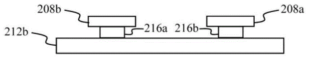
在示例性实施例中,封装件102是圆矩形结构,具有五个表面:一个顶面214和四个侧面212a-d(统称为“侧面212”)。本质上是缺少与顶面214相对的表面的矩形长方体,封装件102可以被认为是敞开式箱体或无盖式箱体。当SMD装配件100被放置在PCB上时,顶面214与侧面212a-d正交并且平行于PCB。相对的侧面212a和212c彼此平行,相对的侧面212b和212d也是如此。相对侧面212a和212c垂直于相对侧面212b和212d,其中侧面212a、212b、212c和212d以矩形形状布置。In the exemplary embodiment,
封装件102包括两个开口210a和210b(统称为“开口210”)。开口210a部分位于顶面214上并且部分位于侧面212b上;开口210b部分位于顶面上并且部分位于侧面212d上。此外,开口210a和210b都在顶面214的同一侧上。在示例性实施例中,开口210使得MOV 104的主体122能够被设置在封装件102内部,而引线106基本上在封装件外部。
在封装件102的外表面上是封装件耳部208a-d(统称为“封装件耳部208”)。封装件耳部208使引线106能够被策略性地放置以允许焊接到PCB上的相应焊盘。因此,封装件耳部208提供表面结构以将引线106保持在抵靠封装件102的外部的位置,从而促进针对MOV 104内部的表面安装自动化,例如拾放。在示例性实施例中,如图2B所示,封装件耳部208的形状为矩形并且从相应的侧面212以距离d从侧面向外延伸。在示例性实施例中,距离d略大于引线106的宽度w。On the outer surface of
图2C示出了SMD装配件100的侧面212b,以及封装件耳部208b和208a。在一些实施例中,在SMD装配件100的侧视图和透视图中不可见的是耳部连接器216a和216b(统称为“耳部连接器216”),它们本身为矩形形状。耳部连接器216确保封装件耳部208与相应的侧面212间隔距离d,使得宽度为w的引线106能够围绕耳部连接器缠绕。在示例性实施例中,封装件102、四个耳部连接器216和四个封装件耳部208诸如通过注射成型或类似技术被形成为整体结构。Figure 2C shows
图3A-3C是根据示例性实施例的SMD装配件300的代表图。图3A是SMD装配件300的透视图;图3B是SMD装配件的侧视图;和图3C是SMD装配件的一侧的详细视图。与SMD装配件100一样,SMD装配件300也被称为水平SMD装配件。与SMD装配件100相比,SMD装配件300的特征在于扁平的引线。在其他方面,两个SMD装配件100和300是相同的。3A-3C are representative views of an
在图3A和3B中,示出了引线306a和306b(统称为“引线306”)。在示例性实施例中,每根引线306的一部分是扁平的,以助于将引线放置在PCB的指定焊盘上。对于引线306a,被布置在封装件耳部208a-b和侧面212b之间的引线部分318a是扁平的。同样,对于引线306b,被布置在封装件耳部208c-d和侧面212d之间的引线部分318b(统称为“引线部分318”)是扁平的。在示例性实施例中,扁平的引线部分318增加了引线306的表面积,这有助于将SMD装配件300成功地附接到PCB的指定焊盘。此外,在示例性实施例中,通过具有扁平引线,SMD装配件300与PCB共面,这也有助于将SMD装配件成功地附接到PCB的指定焊盘。In Figures 3A and 3B, leads 306a and 306b (collectively "leads 306") are shown. In the exemplary embodiment, a portion of each lead 306 is flattened to facilitate placement of the lead on a designated pad of the PCB. As with lead 306a,
如图3B所示,在封装件耳部208c-d和侧面212d之间存在距离d。在示例性实施例中,距离d略大于引线106的宽度w。此外,在一些实施例中,引线306的引线部分318的宽度w2略宽于封装件耳部208和相应侧面212之间的宽度w。As shown in Figure 3B, there is a distance d between
图3C的详细视图示出了为什么宽度w和w2的差异没有问题。扁平的引线部分318b被设置在侧面212d的底面320的稍下方。因此,在示例性实施例中,引线部分318被设置在整个SMD装配件300底面的稍下方。此外,封装件耳部208c-d没有到达侧面212d的底面。在示例性实施例中,在引线306和封装件耳部208的宽度w2之间存在一些重叠。The detailed view of Figure 3C shows why the difference in width w and w2 is not a problem.
对于SMD装配件100(图2A-2C),虽然引线106是圆柱形的并且不是扁平的,但是在封装件耳部208a-b和侧面212b之间的部分引线106a以及在封装件耳部208c-d和侧面212d之间的部分引线106b也被设置在SMD装配件的底面下方。因此,在示例性实施例中,尽管要使用的引线106的表面积略小于扁平引线,但是SMD装配件100能够成功地焊接到PCB的指定焊盘。For SMD assembly 100 (FIGS. 2A-2C), although leads 106 are cylindrical and not flat, portions of
图4是根据示例性实施例的用于容纳双引线电子部组件的SMD装配件400的代表图。在示例性实施例中,与上述水平SMD装配件100和300相比,SMD装配件400也被称为垂直SMD装配件。双引线电子组件是金属氧化物变阻器(MOV),以其原始配置显示,也称为通孔技术(THT)配置404a,以及以新型配置显示,也称为表面安装技术(SMT)配置404b(以下称为“MOV 404”)。还示出了用于容纳MOV 404(由MOV主体422和引线406a-b组成)的封装件402。在示例性实施例中,如图所示,MOV 404的引线406a-b被软化和弯曲以适合封装件402(统称为“引线406”)。图11B是根据一些实施例的针对MOV 404b的SMT配置的引线406a和406b的图解。FIG. 4 is a representative view of an
在示例性实施例中,引线406相对于MOV主体422布置在与引线106(图1)不同的位置。在引线106a和106b与圆柱形MOV主体的圆周表面相邻的情况下,引线406与MOV主体422的平坦表面相邻。In an exemplary embodiment, leads 406 are arranged at a different location relative to MOV body 422 than leads 106 ( FIG. 1 ). Where leads 106a and 106b are adjacent to the circumferential surface of the cylindrical MOV body, lead 406 is adjacent to the planar surface of MOV body 422 .
MOV 404被放置在封装件402中以形成SMD装配件400。SMD装配件400A和400B是相反的视图:SMD装配件400A示出了将被放置在印刷电路板(PCB)上的器件,而SMD装配件400B示出了MOV 404暴露的器件。SMD装配件400是自引线的,因为在其THT配置中MOV 404的引线406被用于新的表面安装器件。因此,不需要将额外的引线添加到封装件402。
在示例性实施例中,SMD装配件400将任何双引线电子器件从THT器件转变为SMT器件。由于THT器件被插入通过PCB中的孔并被焊接到另一侧,THT器件占用PCB两侧的空间,而使用SMD装配件封装件的同一器件将消耗PCB一侧的空间。此外,PCB不需要像通孔器件那样在其中钻孔。SMD装配件400还被适用于已经成为SMT组件常见的拾放自动化技术。在示例性实施例中,SMD装配件400通过允许高速装配和低成本来提高PCB制造。In an exemplary embodiment, the
在示例性实施例中,水平SMD装配件100和300以及垂直SMD装配件400(以及下面示出和描述的垂直SMD装配件600)可用于响应客户请求。在示例性实施例中,与垂直SMD装配件相比,水平SMD装配件具有略大的覆盖区,并且因此当放置在PCB上时消耗更多的表面空间。相比之下,与水平SMD装配件相比,垂直SMD装配件在垂直于PCB表面的方向上(例如,垂直)略高。特别是对于受尺寸和空间限制的电路,替代品的可用性为客户提供了灵活性。因此,水平和垂直SMD装配件在设计电路时给予了客户选择。In an exemplary embodiment,
图5A-5C是根据示例性实施例的SMD装配件400的代表图。图5A是SMD装配件400的透视图;图5B是SMD装配件的侧视图;图5C是SMD装配件一侧的详细视图。在图5A和5B中,MOV404被暴露。SMD装配件400的特征在于来自图4的封装件402、MOV 404和引线406。在示例性实施例中,封装件402由刚性塑料材料制成。在一个实施例中,封装件402是热塑性塑料,例如聚酰胺。5A-5C are representative views of an
如图4所示,MOV 404的引线406被布置在SMT配置中。引线406是圆柱形的并且由导电材料制成。在示例性实施例中,一旦将SMD装配件400放置在PCB表面的指定焊盘上(诸如使用拾放或一些其他自动化方法),引线406将被焊接到PCB表面的指定焊盘上。一旦如此连接并且将电源应用到所得电路,MOV 404将被电连接到同样被焊接在PCB上的其他组件。As shown in FIG. 4 , leads 406 of
在示例性实施例中,封装件402是圆矩形结构,其具有五个侧面,一个顶面514和四个侧面512a-d(统称为“侧面512”)。本质上是缺少与顶面214相对的表面的矩形长方体,封装件402可以被认为是敞开式箱体或无盖式箱体。当SMD装配件400被放置在PCB上时,顶面514与侧面512a-d正交并且平行于PCB。相对的侧面512a和512c彼此平行,相对的侧面512b和512d也是如此。相对侧面512a和512c垂直于相对侧面512b和512d,其中侧面512a、512b、512c和512d以矩形形状布置。In the exemplary embodiment,
封装件402包括两个开口510a和510b(统称为“开口510”)。如图1所示,MOV 104的引线106被布置在SMT配置中。开口510a部分位于顶面514上并且部分位于侧面512d上;开口510b部分位于顶面上并且部分位于侧面512b上。与开口210a和210b相比,开口510a和510b位于顶面514的相对侧。在示例性实施例中,开口510使MOV 404的主体422能够设置在封装件402内部,而引线406基本上位于封装件外部。
在封装件402的外表面上是封装件耳部508a-d(统称为“封装件耳部508”)。封装件耳部508使引线406能够被策略性地放置以允许焊接到PCB上的相应焊盘。在示例性实施例中,如图5所示,封装件耳部508为矩形形状并且从相应的侧面512以距离d从侧面向外延伸。在示例性实施例中,距离d略大于引线406的宽度w。On the outer surface of
图5C示出了SMD装配件400的侧面512d以及封装件耳部508c和508d。在一些实施例中,在SMD装配件400的侧视图和透视图中不可见的是耳部连接器516a和516b(统称为“耳部连接器516”),它们本身为矩形形状。耳部连接器516确保封装件耳部508与相应的侧面512间隔距离d,使得宽度为w的引线406能够围绕耳部连接器缠绕。在示例性实施例中,封装件402、四个耳部连接器516和四个封装件耳部508诸如通过注射成型或类似技术被形成为整体结构。FIG. 5C shows
图6A-6C是根据示例性实施例的SMD装配件600的代表图。图6A是SMD装配件600的透视图;图6B是SMD装配件的侧视图;图6C是SMD装配件一侧的详细视图。与SMD装配件500相比,SMD装配件600的特征在于扁平的引线。在其他方面,两个SMD装配件500和600是相同的。6A-6C are representative views of an SMD assembly 600 according to an exemplary embodiment. Figure 6A is a perspective view of the SMD assembly 600; Figure 6B is a side view of the SMD assembly; Figure 6C is a detailed view of one side of the SMD assembly. Compared to SMD assembly 500 , SMD assembly 600 is characterized by flat leads. In other respects, the two SMD assemblies 500 and 600 are identical.
在图6A和6B中,示出了引线606a和606b(统称为“引线606”)。在示例性实施例中,每根引线606的一部分是扁平的,以助于将引线放置在PCB的指定焊盘上。对于引线606a,设置在封装件耳部508a-b和侧面512b之间的引线部分618a是扁平的。同样,对于引线606b,设置在封装件耳部508c-d和侧面512d之间的引线部分618b(统称为“引线部分618”)是扁平的。在示例性实施例中,扁平的引线部分618增加了引线606的表面积,这有助于将SMD装配件600成功地附接到PCB的指定焊盘。此外,在示例性实施例中,通过具有扁平引线,SMD装配件600与PCB共面,这也有助于将SMD装配件成功附接到PCB的指定焊盘。In Figures 6A and 6B, leads 606a and 606b (collectively "leads 606") are shown. In the exemplary embodiment, a portion of each lead 606 is flattened to facilitate placement of the lead on a designated pad of the PCB. As with lead 606a,
如图6B所示,封装件耳部508a-b和侧面512b之间存在距离d。在示例性实施例中,距离d略大于引线606的宽度w。此外,在一些实施例中,引线606的引线部分618的宽度w2略宽于封装件耳部508和相应侧面512之间的宽度w。As shown in Figure 6B, there is a distance d between
图6C的详细视图示出了为什么宽度w和w2的差异没有问题。扁平的引线部分618b被设置在侧面512b的底面620的稍下方。因此,在示例性实施例中,引线部分618被设置在整个SMD装配件600的底面的稍下方。此外,封装件耳部508a-b没有到达侧面512b的底面。在示例性实施例中,在引线606的宽度w2和封装件耳部508之间存在一些重叠。The detailed view of Figure 6C shows why the difference in width w and w2 is not a problem.
对于SMD装配件500(图5A-5C),尽管引线406是圆柱形且不是扁平的,但在封装件耳部508a-b和侧面512b之间的部分引线406a以及在封装件耳部508c-d和侧面512d之间的部分引线406b也被设置在SMD装配件的底面下方。因此,在示例性实施例中,尽管与扁平引线相比,可使用的引线406表面积稍小,但SMD装配件400能够成功地焊接到PCB的指定焊盘。For SMD assembly 500 (FIGS. 5A-5C), although lead 406 is cylindrical and not flat, part of lead 406a between
图7A-7D是根据示例性实施例的针对水平SMD装配件100/300的封装件102的代表图。图7A是封装件102的俯视图;图7B是封装件的侧视图;图7C是在PCB上的建议的封装件和焊盘布局702;并且图7D是封装件的第二侧视图。封装件102以及封装件和焊盘布局702的尺寸以毫米给出并且不意味着限制。在示例性实施例中,举几个来说,SMD装配件100/300支持5mm、7mm、10mm、14mm、20mm、25mm、D7mm、D14mm和D20mm的MOV芯片直径。因此,SMD装配件100/300的封装件102可缩放以支持多种MOV尺寸。图7A-7D的尺寸是根据一些实施例的对封装件102以及封装件和焊盘布局702的说明。然而,对于SMD装配件100/300的封装件102的每个尺寸,多个不同的MOV可以在其中适应。因此,在示例性实施例中,SMD装配件100/300的特征在于“通用尺寸(one-size-fits-most)”封装件。7A-7D are representative views of
除了根据示例性实施例提供尺寸信息之外,还示出了封装件放置704以及焊盘位置706a和706b(统称为“焊盘位置706”),诸如用于PCB布局(图7C)。图7B还示出了扁平的引线说明708,其将适用于SMD装配件300但不适用于SMD装配件100。无论使用非扁平(圆柱形)引线106或是扁平引线306,引线的焊接面的共面度(coplanarity)都可控制为小于0.1mm,其中,导线引线的直径通常为0.8mm至1mm。In addition to providing dimensional information according to an exemplary embodiment,
图8A-8D是根据示例性实施例的针对垂直SMD装配件400/600的封装件402的代表图。图8A是封装件402的俯视图;图8B是封装件的侧视图;图8C是PCB上的建议的封装件和焊盘布局802;以及图8D是封装件的第二侧视图。封装件402以及封装件和焊盘布局802的尺寸以毫米给出并且不意味着限制。在示例性实施例中,举几个来说,SMD装配件400/600支持5mm、7mm、10mm、14mm、20mm、25mm、D7mm、D14mm和D20mm的MOV芯片直径。与SMD装配件100/300一样,SMD装配件400/600的封装件402可缩放以支持多种MOV尺寸。图8A-8D的尺寸是根据一些实施例的对封装件402以及封装件和焊盘布局802的说明。然而,对于SMD装配件400/600的封装件402的每个尺寸,多个不同的MOV可以适应其中。因此,在示例性实施例中,SMD装配件400/600的特征在于“通用尺寸”封装件。8A-8D are representative views of a
除了根据示例性实施例提供尺寸信息之外,还示出了封装件放置804以及焊盘位置806a和806b(统称为“焊盘位置806”),诸如用于PCB布局(图8C)。图8B还示出了扁平的引线说明808,其将适用于SMD装配件600但不适用于SMD装配件400。无论使用非扁平(圆柱形)引线406或是扁平引线606,引线的焊接面的共面度都可控制为小于0.1mm,其中,引线的直径通常为0.8mm至1mm。In addition to providing dimensional information according to an exemplary embodiment,
在一些实施例中,查看封装件和焊盘布局702(图7C)以及封装件和焊盘布局802(图8C),水平SMD装配件100/300在PCB上的覆盖区大于垂直SMD装配件400/600的覆盖区。水平SMD装配件100/300(图7B)的高度小于垂直SMD装配件400/600(图8B)的高度。因此,客户可以根据给定的电路设计灵活地在水平SMD装配件和垂直SMD装配件之间进行选择。In some embodiments, looking at package and pad layout 702 ( FIG. 7C ) and package and pad layout 802 ( FIG. 8C ),
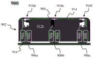
图9A-9B是根据示例性实施例的用于容纳多个双引线电子组件的SMD装配件900的代表图。图9A是SMD装配件900的透视图;图9B是SMD装配件的侧视图。在示例性实施例中,SMD装配件900也被称为水平SMD装配件。用于容纳多个双引线电子组件的垂直SMD装配件未在文中示出,尽管它可以共享SMD装配件900以及垂直SMD装配件300/600的特征。包含在SMD装配件900的封装件902中的三个双引线电子组件是MOV 904,尽管它们大部分从视图中被遮蔽。MOV 104的四个引线906a-d(统称为“引线906”)是可见的。在示例性实施例中,引线906被软化和弯曲以适应到封装件902中。9A-9B are representative views of an
与在文中示出和描述的其他SMD装配件一样,SMD装配件900的引线906是圆柱形的并且由导电材料制成。在示例性实施例中,一旦将SMD装配件900放置在PCB表面916的指定焊盘上(诸如使用拾放或一些其他自动化方法),引线906将被焊接到PCB表面916(图9B)的指定焊盘上。一旦如此连接并且电源被应用到所得电路,MOV 904将被电连接到同样被焊接在PCB 916上的其他组件。Like the other SMD assemblies shown and described herein, the
在示例性实施例中,封装件902是圆矩形结构,其具有五个侧面,一个顶面914和四个侧面912a-d(统称为“侧面912”)。本质上是缺少与顶面814相对的表面的矩形长方体,封装件902可以被认为是敞开式箱体或无盖式箱体。当SMD装配件900被放置在PCB上时,顶面914与侧面912a-d正交并且平行于PCB。相对的侧面912a和912c彼此平行,相对的侧面912b和912d也是如此。相对侧面912a和912c垂直于相对侧面912b和912d,其中侧面912a、912b、912c和912d以矩形形状布置。In the exemplary embodiment,
封装件902包括六个开口910a-f(统称为“开口910”)。开口910a-c部分位于顶面914上并且部分位于侧面912d上;开口910d-f部分位于顶面上并且部分位于侧面912b上。在示例性实施例中,开口910使得三个MOV 904的主体能够被设置在封装件902内部,而引线906基本上在封装件外部。
在封装件902的外表面上是封装件耳部908a-f(统称为“封装件耳部908”),其在侧面912b上是可见的,并且封装件耳部在侧面912d上是不可见的。封装件耳部908使引线906能够被策略性地放置以允许焊接到PCB 916上的相应焊盘。在示例性实施例中,封装件耳部908为矩形形状并且从相应的侧面912向外延伸。与封装件耳部208和508相反,封装件耳部908成对设置。在侧面912b上,封装件耳部908a和908b保持引线906a;封装件耳部908c和908d保持引线906b;以及封装件耳部908e和908f保持引线906c,类似的配置也出现在侧面912d上。On the outer surface of
在一些实施例中,可以交换配置,使得SMD装配件100、300、400和600中的任何一个使用两部分的封装件耳部(例如,图9A),而SMD装配件900使用一部分的封装件耳部208或508(例如,图2A)。示例性实施例中,尽管不可见,但SMD装配件900的特征在于耳部连接器(例如,图2C)。在示例性实施例中,封装件902、耳部连接器和封装件耳部908被形成为整体结构,诸如通过注射成型或类似技术。在一些实施例中,虽然SMD装配件900支持三个MOV,但本文所示和描述的原理可以被应用于容纳任意数量的双引线电子组件的SMD装配件。In some embodiments, configurations can be exchanged so that any of the
图10A和10B是根据示例性实施例的针对SMD装配件900的尺寸的代表图。图10A是SMD装配件900的侧视图;并且图10B是SMD装配件的第二侧视图。SMD装配件900的尺寸以毫米给出并且不意味着限制。在示例性实施例中,SMD装配件900可缩放以支持多种MOV尺寸。因此,在示例性实施例中,SMD装配件900的特征在于“通用尺寸”封装件。10A and 10B are representative diagrams for dimensions of an
在示例性实施例中,SMD装配件900的侧面912a-d的高度在13.5mm和14mm之间(图10A),并且侧面912a和912c的宽度是18.0mm,其中包括封装件耳部908的总宽度在20.9mm和21.5mm之间(图10B)。图10A还示出了扁平的引线说明1002,尽管SMD装配件900可以具有圆柱形引线或扁平引线。无论使用非扁平(圆柱形)引线406或是扁平引线606,引线的焊接面的共面度都可控制为小于0.1mm,其中,引线的直径通常为0.8mm至1mm。In an exemplary embodiment, the height of the
图11A和11B是根据示例性实施例的图1和4的相应SMT MOV的引线的代表图。图11A的特征在于用于MOV 104b的SMT配置的引线106a和106b。图11B的特征在于用于MOV 404b的SMT配置的引线406a和406b。引线106a和106b被示出为相对于彼此在MOV 104(未示出)的任一侧的位置。类似地,引线406a和406b被示出为相对于彼此在MOV 404(未示出)的任一侧的位置。11A and 11B are representative diagrams of leads of the respective SMT MOVs of FIGS. 1 and 4, according to an exemplary embodiment. FIG. 11A features leads 106a and 106b for the SMT configuration of
每根引线106/406包括内部部分1102、表面安装部分1104以及封装件耳部部分1106。内部部分1102是保留在SMD装配件的封装件102/402的内部的引线106/406的一部分;表面安装部分1104是要被焊接到PCB上的焊盘的引线的一部分;并且封装件耳部部份1106是围绕或以其他方式连接到SMD装配件的封装件耳部208/508的引线的一部分。图11A和11B所示的引线配置并不意味着限制,因为本文描述的SMD装配件可以使用不同形状的引线。Each lead 106 / 406 includes an
图12是根据示例性实施例的SMD装配件900(图9A和9B)的引线的代表图。引线906被示出为相对于彼此在MOV 904(未示出)的任一侧的位置。FIG. 12 is a representative view of the leads of the SMD assembly 900 ( FIGS. 9A and 9B ) according to an exemplary embodiment.
每根引线906包括内部部分1202、表面安装部分1204和封装件耳部部分1206。内部部分1202是保留在SMD装配件900的封装件902内部的引线906的一部分;表面安装部分1204是要被焊接到PCB上的焊盘的引线的一部分;并且封装件耳部部分1206是围绕或以其他方式连接到SMD装配件的封装件耳部908的引线的一部分。图12中所示的引线配置并不意味着是限制,因为本文描述的SMD装配件可以使用不同形状的引线。Each
当被放置在PCB上时,本文所示和描述的自引线SMD装配件提供了优于THT类型电子组件的多个优点。使用SMD装配件封装可以实现高效率和低成本的自动化电子组件装配线。该封装支持广泛的电压范围,从低压到高压电子组件。该封装还支持不同尺寸的电子组件。提供水平和垂直类型SMD装配件以供最佳客户选择。When placed on a PCB, the self-leaded SMD assembly shown and described herein offers several advantages over THT type electronic assemblies. The use of SMD assembly packaging enables efficient and low-cost automated electronic component assembly lines. The package supports a wide range of voltages, from low voltage to high voltage electronic components. The package also supports electronic components of different sizes. Provide horizontal and vertical type SMD assembly for best customer choice.
制造工艺manufacturing process
图13是根据示例性实施例的用于制造自引线SMD装配件100、400和900的代表流程图,并且图14A-D是用于说明在图13中描述的一些工艺步骤的代表图。在示例性实施例中,多个电子组件的引线是扁平的(框1302)。可替换地,部分引线是扁平的,即,部分引线将要被焊接到PCB。这是可选的步骤,因为自引线装配件100、400和900也可以在没有偏平引线的情况下焊接到PCB。FIG. 13 is a representative flowchart for fabricating self-
在示例性实施例中,电子组件以卷带式封装(tape and reel packaging)进行装配(框1304)。卷带式是一种由具有单独腔体用于保持每个电子组件的承载带组成的制造方法。电子组件的顺序阵列因此被布置在承载带中。然后用覆盖带将电子组件固定在腔体内,形成一个卷轴,很像电影卷轴。卷带式方法使电子组件易于储存和运输。卷轴被附接到SMD装配机的线轴上,其中,电子组件从其腔体中单独移除并被焊接到印刷电路板。图14A是MOV器件的卷带式装配件的图解。In an exemplary embodiment, the electronic assembly is assembled in tape and reel packaging (block 1304). Tape and Reel is a manufacturing method consisting of a carrier tape with individual cavities for holding each electronic component. A sequential array of electronic components is thus arranged in the carrier tape. Cover tape is then used to secure the electronic assembly within the cavity, forming a reel, much like a movie reel. The tape and reel method allows for easy storage and transportation of electronic assemblies. The spool is attached to the spool of the SMD assembly machine where the electronic components are individually removed from their cavities and soldered to the printed circuit board. Figure 14A is an illustration of a tape and reel assembly of an MOV device.
然后将电子组件的带条和卷轴送入SMD装配机中(框1306)。在那里,每个电子组件的引线被可选地切割和弯曲(框1308)。回想一下,相应SMD装配件100、400和900的封装件102、402和902被设计成支持具有不同尺寸的电子组件。例如,小的MOV被弯曲以适应封装件,其引线不会被切割,然而较大的MOV的引线可能会被切割。因此,在此步骤中引线的切割是可选的。然而,为了适应封装件,所有引线都被弯曲。图14B是具有弯曲引线的MOV104/404/904的图解。The tape and reel of electronic assemblies are then fed into the SMD assembly machine (block 1306). There, the leads of each electronic component are optionally cut and bent (block 1308). Recall that the
一旦引线弯曲,每个电子组件都被装配到相应的封装件中(框1310)。图14C示出了被放置在塑料封装件102/402/902中的MOV 104/404/904。现在伸出封装件的引线接下来缠绕在封装件102/402/902的封装件耳部周围(框1312)。同样,在一些实施例中,因为本文所示和描述的封装件支持多种尺寸和形状的电子器件,引线的圈数是变化的。此外,引线的缠绕将根据封装件耳部是分开的(如在SMD装配件100(图1)中)还是靠近在一起(如在SMD装配件400(图4)和900(图9A)中)而变化。图14D示出了缠绕在封装件耳部周围的引线。在一些实施例中,添加黏合胶以将电子器件的主体固定到封装件(框1314)。Once the leads are bent, each electronic component is assembled into a corresponding package (block 1310). FIG. 14C shows
一旦电子器件被完全装配,就对每个自引线组件执行功能测试以确保该器件工作(框1316)。还执行平整度检查,以便可以将自引线组件焊接到PCB,作为表面安装器件(框1318)。在示例性实施例中,然后将自引线组件装配到卷带式封装件的专用腔体中,形成用于自引线组件的SMD装配件的新卷轴(框1320)。Once the electronic device is fully assembled, functional testing is performed on each self-leaded assembly to ensure that the device works (block 1316). A flatness check is also performed so that the self-leaded assembly can be soldered to the PCB as a surface mount device (block 1318). In an exemplary embodiment, the self-leaded components are then assembled into dedicated cavities of the tape and reel package, forming a new reel of SMD assemblies for the self-leaded components (block 1320).
如本文所使用的,以单数形式叙述并以单词“一”或“一个”开头的元件或步骤应该被理解为不排除复数元件或步骤,除非明确叙述了这种排除。此外,对本公开的“一个实施例”的引用并不旨在被解释为排除也结合了所述特征的附加实施例的存在。As used herein, an element or step recited in the singular and proceeded with the word "a" or "an" should be understood as not excluding plural elements or steps, unless such exclusion is explicitly recited. Furthermore, references to "one embodiment" of the present disclosure are not intended to be interpreted as excluding the existence of additional embodiments that also incorporate the recited features.
虽然本公开参考了某些实施例,但在不脱离如所附权利要求中限定的本公开的领域和范围的情况下,对所描述的实施例的多种修改、替换和改变是可能的。因此,意图是本公开不限于所描述的实施例,而是具有由以下权利要求的语言及其等同物限定的全部范围。Although this disclosure refers to certain embodiments, various modifications, substitutions and changes to the described embodiments are possible without departing from the sphere and scope of the disclosure as defined in the appended claims. Accordingly, it is intended that the disclosure not be limited to the described embodiments, but that it have the full scope defined by the language of the following claims and their equivalents.
Claims (20)
Priority Applications (1)
| Application Number | Priority Date | Filing Date | Title |
|---|---|---|---|
| CN202111093133.4A CN115835618A (en) | 2021-09-17 | 2021-09-17 | Self-leaded SMD package |
Applications Claiming Priority (1)
| Application Number | Priority Date | Filing Date | Title |
|---|---|---|---|
| CN202111093133.4A CN115835618A (en) | 2021-09-17 | 2021-09-17 | Self-leaded SMD package |
Publications (1)
| Publication Number | Publication Date |
|---|---|
| CN115835618A true CN115835618A (en) | 2023-03-21 |
Family
ID=85515848
Family Applications (1)
| Application Number | Title | Priority Date | Filing Date |
|---|---|---|---|
| CN202111093133.4A Pending CN115835618A (en) | 2021-09-17 | 2021-09-17 | Self-leaded SMD package |
Country Status (1)
| Country | Link |
|---|---|
| CN (1) | CN115835618A (en) |
Cited By (1)
| Publication number | Priority date | Publication date | Assignee | Title |
|---|---|---|---|---|
| CN119865970A (en) * | 2025-03-25 | 2025-04-22 | 珠海华冠电容器股份有限公司 | Vehicle-gauge-level multi-lead SMD (surface mounted device) package and preparation method thereof |
Citations (12)
| Publication number | Priority date | Publication date | Assignee | Title |
|---|---|---|---|---|
| GB9821659D0 (en) * | 1998-10-05 | 1998-11-25 | Standex Int Corp | Surface mount electronic reed switch component with transverse lead wire loops |
| US6428349B1 (en) * | 2001-04-30 | 2002-08-06 | Hewlett-Packard Company | Method and apparatus for jumpering resistors and other components on a printed circuit board |
| US20060021792A1 (en) * | 2004-07-28 | 2006-02-02 | Myers Bruce A | Surface mount axial leaded component for an electronic module |
| US20080259580A1 (en) * | 2007-04-20 | 2008-10-23 | Stillabower Morris D | Method for mounting leaded component to substrate |
| JP3149018U (en) * | 2007-09-17 | 2009-03-12 | レイケム エレクトロニクス シャンハイ リミテッド | Housing and mounting parts |
| CN101563813A (en) * | 2006-12-22 | 2009-10-21 | 泰科电子公司 | Small cross-section surface mount poke-in connector |
| WO2015195223A1 (en) * | 2014-06-18 | 2015-12-23 | Illinois Tool Works Inc. | Two-high light-emitting diode holder structure |
| US20160133797A1 (en) * | 2014-11-06 | 2016-05-12 | Powerled Electronic Co., Ltd. | SMD Type LED Package Device, Method for Manufacturing the Same, and Light-Emitting Apparatus |
| US20160374214A1 (en) * | 2015-06-19 | 2016-12-22 | Circor Aerospace, Inc. | Miniature smt housing for electronics package |
| CN112786559A (en) * | 2019-11-11 | 2021-05-11 | 德克萨斯仪器股份有限公司 | Packaged device carrier for thermal enhancement or signal redistribution of packaged semiconductor devices |
| CN113035473A (en) * | 2021-02-06 | 2021-06-25 | 安徽省昌盛电子有限公司 | Double-cap SMD wire-wound chip resistor capable of avoiding alloy wire fracture at welding spot |
| CN218337042U (en) * | 2021-09-17 | 2023-01-17 | 东莞令特电子有限公司 | Surface mount device assembly |
-
2021
- 2021-09-17 CN CN202111093133.4A patent/CN115835618A/en active Pending
Patent Citations (12)
| Publication number | Priority date | Publication date | Assignee | Title |
|---|---|---|---|---|
| GB9821659D0 (en) * | 1998-10-05 | 1998-11-25 | Standex Int Corp | Surface mount electronic reed switch component with transverse lead wire loops |
| US6428349B1 (en) * | 2001-04-30 | 2002-08-06 | Hewlett-Packard Company | Method and apparatus for jumpering resistors and other components on a printed circuit board |
| US20060021792A1 (en) * | 2004-07-28 | 2006-02-02 | Myers Bruce A | Surface mount axial leaded component for an electronic module |
| CN101563813A (en) * | 2006-12-22 | 2009-10-21 | 泰科电子公司 | Small cross-section surface mount poke-in connector |
| US20080259580A1 (en) * | 2007-04-20 | 2008-10-23 | Stillabower Morris D | Method for mounting leaded component to substrate |
| JP3149018U (en) * | 2007-09-17 | 2009-03-12 | レイケム エレクトロニクス シャンハイ リミテッド | Housing and mounting parts |
| WO2015195223A1 (en) * | 2014-06-18 | 2015-12-23 | Illinois Tool Works Inc. | Two-high light-emitting diode holder structure |
| US20160133797A1 (en) * | 2014-11-06 | 2016-05-12 | Powerled Electronic Co., Ltd. | SMD Type LED Package Device, Method for Manufacturing the Same, and Light-Emitting Apparatus |
| US20160374214A1 (en) * | 2015-06-19 | 2016-12-22 | Circor Aerospace, Inc. | Miniature smt housing for electronics package |
| CN112786559A (en) * | 2019-11-11 | 2021-05-11 | 德克萨斯仪器股份有限公司 | Packaged device carrier for thermal enhancement or signal redistribution of packaged semiconductor devices |
| CN113035473A (en) * | 2021-02-06 | 2021-06-25 | 安徽省昌盛电子有限公司 | Double-cap SMD wire-wound chip resistor capable of avoiding alloy wire fracture at welding spot |
| CN218337042U (en) * | 2021-09-17 | 2023-01-17 | 东莞令特电子有限公司 | Surface mount device assembly |
Cited By (1)
| Publication number | Priority date | Publication date | Assignee | Title |
|---|---|---|---|---|
| CN119865970A (en) * | 2025-03-25 | 2025-04-22 | 珠海华冠电容器股份有限公司 | Vehicle-gauge-level multi-lead SMD (surface mounted device) package and preparation method thereof |
Similar Documents
| Publication | Publication Date | Title |
|---|---|---|
| US6501270B1 (en) | Hall effect sensor assembly with cavities for integrated capacitors | |
| JP2987101B2 (en) | Method for connecting semiconductor device and connector for semiconductor device | |
| US8593825B2 (en) | Apparatus and method for vertically-structured passive components | |
| US7891980B2 (en) | Interconnect device with discrete in-line components | |
| US20080266824A1 (en) | Pad and circuit board, electronic device using same | |
| CN218337042U (en) | Surface mount device assembly | |
| JP3703521B2 (en) | Pin socket connector for board mounting | |
| CN102044531B (en) | Apparatus and method for vertically-structured passive components | |
| US20020132533A1 (en) | Discrete device socket and method of fabrication therefor | |
| CN115835618A (en) | Self-leaded SMD package | |
| US10098231B2 (en) | Integrated electronic assembly for conserving space in a circuit | |
| TW201904154A (en) | Printed circuit board embedded protection components | |
| JP2544976B2 (en) | Semiconductor integrated circuit module | |
| JPH10313157A (en) | Printed board | |
| CN103460816A (en) | Electronic assembly | |
| CN112737272B (en) | A base welded with electronic components and its production process and voice coil motor | |
| US20020055283A1 (en) | Multiple line grid connector | |
| JP2570336B2 (en) | Hybrid integrated circuit device | |
| CN216749487U (en) | Double-device module | |
| CN113258326B (en) | Inspection socket | |
| JP3869434B2 (en) | Surface mount package and method of manufacturing the same | |
| CN219393074U (en) | Surface mount device module | |
| CN223414073U (en) | Circuit packaging structure | |
| US20250336576A1 (en) | Three-dimensional electrodes for reflowable ptc device | |
| US12302492B2 (en) | Interposer for active implantable medical device |
Legal Events
| Date | Code | Title | Description |
|---|---|---|---|
| PB01 | Publication | ||
| PB01 | Publication | ||
| SE01 | Entry into force of request for substantive examination | ||
| SE01 | Entry into force of request for substantive examination |