CN115810369A - Storage system and storage system control method - Google Patents
Storage system and storage system control method Download PDFInfo
- Publication number
- CN115810369A CN115810369A CN202210208507.0A CN202210208507A CN115810369A CN 115810369 A CN115810369 A CN 115810369A CN 202210208507 A CN202210208507 A CN 202210208507A CN 115810369 A CN115810369 A CN 115810369A
- Authority
- CN
- China
- Prior art keywords
- data
- power supply
- volatile memory
- controller
- size
- Prior art date
- Legal status (The legal status is an assumption and is not a legal conclusion. Google has not performed a legal analysis and makes no representation as to the accuracy of the status listed.)
- Pending
Links
Images


Classifications
-
- G—PHYSICS
- G11—INFORMATION STORAGE
- G11C—STATIC STORES
- G11C11/00—Digital stores characterised by the use of particular electric or magnetic storage elements; Storage elements therefor
- G11C11/21—Digital stores characterised by the use of particular electric or magnetic storage elements; Storage elements therefor using electric elements
- G11C11/34—Digital stores characterised by the use of particular electric or magnetic storage elements; Storage elements therefor using electric elements using semiconductor devices
- G11C11/40—Digital stores characterised by the use of particular electric or magnetic storage elements; Storage elements therefor using electric elements using semiconductor devices using transistors
- G11C11/401—Digital stores characterised by the use of particular electric or magnetic storage elements; Storage elements therefor using electric elements using semiconductor devices using transistors forming cells needing refreshing or charge regeneration, i.e. dynamic cells
- G11C11/4063—Auxiliary circuits, e.g. for addressing, decoding, driving, writing, sensing or timing
- G11C11/407—Auxiliary circuits, e.g. for addressing, decoding, driving, writing, sensing or timing for memory cells of the field-effect type
- G11C11/409—Read-write [R-W] circuits
- G11C11/4093—Input/output [I/O] data interface arrangements, e.g. data buffers
-
- G—PHYSICS
- G11—INFORMATION STORAGE
- G11C—STATIC STORES
- G11C14/00—Digital stores characterised by arrangements of cells having volatile and non-volatile storage properties for back-up when the power is down
- G11C14/0009—Digital stores characterised by arrangements of cells having volatile and non-volatile storage properties for back-up when the power is down in which the volatile element is a DRAM cell
-
- G—PHYSICS
- G06—COMPUTING OR CALCULATING; COUNTING
- G06F—ELECTRIC DIGITAL DATA PROCESSING
- G06F1/00—Details not covered by groups G06F3/00 - G06F13/00 and G06F21/00
- G06F1/26—Power supply means, e.g. regulation thereof
- G06F1/30—Means for acting in the event of power-supply failure or interruption, e.g. power-supply fluctuations
-
- G—PHYSICS
- G11—INFORMATION STORAGE
- G11C—STATIC STORES
- G11C11/00—Digital stores characterised by the use of particular electric or magnetic storage elements; Storage elements therefor
- G11C11/21—Digital stores characterised by the use of particular electric or magnetic storage elements; Storage elements therefor using electric elements
- G11C11/34—Digital stores characterised by the use of particular electric or magnetic storage elements; Storage elements therefor using electric elements using semiconductor devices
- G11C11/40—Digital stores characterised by the use of particular electric or magnetic storage elements; Storage elements therefor using electric elements using semiconductor devices using transistors
- G11C11/401—Digital stores characterised by the use of particular electric or magnetic storage elements; Storage elements therefor using electric elements using semiconductor devices using transistors forming cells needing refreshing or charge regeneration, i.e. dynamic cells
- G11C11/4063—Auxiliary circuits, e.g. for addressing, decoding, driving, writing, sensing or timing
- G11C11/407—Auxiliary circuits, e.g. for addressing, decoding, driving, writing, sensing or timing for memory cells of the field-effect type
- G11C11/4074—Power supply or voltage generation circuits, e.g. bias voltage generators, substrate voltage generators, back-up power, power control circuits
-
- G—PHYSICS
- G11—INFORMATION STORAGE
- G11C—STATIC STORES
- G11C11/00—Digital stores characterised by the use of particular electric or magnetic storage elements; Storage elements therefor
- G11C11/21—Digital stores characterised by the use of particular electric or magnetic storage elements; Storage elements therefor using electric elements
- G11C11/34—Digital stores characterised by the use of particular electric or magnetic storage elements; Storage elements therefor using electric elements using semiconductor devices
- G11C11/40—Digital stores characterised by the use of particular electric or magnetic storage elements; Storage elements therefor using electric elements using semiconductor devices using transistors
- G11C11/401—Digital stores characterised by the use of particular electric or magnetic storage elements; Storage elements therefor using electric elements using semiconductor devices using transistors forming cells needing refreshing or charge regeneration, i.e. dynamic cells
- G11C11/4063—Auxiliary circuits, e.g. for addressing, decoding, driving, writing, sensing or timing
- G11C11/407—Auxiliary circuits, e.g. for addressing, decoding, driving, writing, sensing or timing for memory cells of the field-effect type
- G11C11/409—Read-write [R-W] circuits
- G11C11/4096—Input/output [I/O] data management or control circuits, e.g. reading or writing circuits, I/O drivers or bit-line switches
-
- G—PHYSICS
- G11—INFORMATION STORAGE
- G11C—STATIC STORES
- G11C5/00—Details of stores covered by group G11C11/00
- G11C5/14—Power supply arrangements, e.g. power down, chip selection or deselection, layout of wirings or power grids, or multiple supply levels
- G11C5/141—Battery and back-up supplies
-
- G—PHYSICS
- G11—INFORMATION STORAGE
- G11C—STATIC STORES
- G11C5/00—Details of stores covered by group G11C11/00
- G11C5/14—Power supply arrangements, e.g. power down, chip selection or deselection, layout of wirings or power grids, or multiple supply levels
- G11C5/143—Detection of memory cassette insertion or removal; Continuity checks of supply or ground lines; Detection of supply variations, interruptions or levels ; Switching between alternative supplies
-
- Y—GENERAL TAGGING OF NEW TECHNOLOGICAL DEVELOPMENTS; GENERAL TAGGING OF CROSS-SECTIONAL TECHNOLOGIES SPANNING OVER SEVERAL SECTIONS OF THE IPC; TECHNICAL SUBJECTS COVERED BY FORMER USPC CROSS-REFERENCE ART COLLECTIONS [XRACs] AND DIGESTS
- Y02—TECHNOLOGIES OR APPLICATIONS FOR MITIGATION OR ADAPTATION AGAINST CLIMATE CHANGE
- Y02D—CLIMATE CHANGE MITIGATION TECHNOLOGIES IN INFORMATION AND COMMUNICATION TECHNOLOGIES [ICT], I.E. INFORMATION AND COMMUNICATION TECHNOLOGIES AIMING AT THE REDUCTION OF THEIR OWN ENERGY USE
- Y02D10/00—Energy efficient computing, e.g. low power processors, power management or thermal management
Landscapes
- Engineering & Computer Science (AREA)
- Microelectronics & Electronic Packaging (AREA)
- Computer Hardware Design (AREA)
- Power Engineering (AREA)
- Theoretical Computer Science (AREA)
- Databases & Information Systems (AREA)
- Physics & Mathematics (AREA)
- General Engineering & Computer Science (AREA)
- General Physics & Mathematics (AREA)
- Techniques For Improving Reliability Of Storages (AREA)
- Power Sources (AREA)
- Memory System (AREA)
Abstract
一个实施方式提供了一种存储系统和存储系统的控制方法,例如,即使在PLP电容器的性能劣化时也可以实现包括PLP功能的存储系统。根据一个实施方式,一种存储系统包括控制将数据写入非易失性存储器和易失性存储器的控制器,电源电路利用由外部提供的第一电压而产生多个电压,并将该多个电压提供给非易失性存储器、易失性存储器、控制器和备用电源电路。在第一电压并非因关机命令而降低时,电源电路利用备用电源电路的输出电压而产生多个电压。控制器按照从备用电源电路馈送的供电能力,来改变可存储在易失性存储器中的数据的大小。
One embodiment provides a storage system and a control method of the storage system, for example, which can implement a storage system including a PLP function even when the performance of a PLP capacitor is degraded. According to one embodiment, a storage system includes a controller for controlling writing of data into a nonvolatile memory and a volatile memory, a power supply circuit generates a plurality of voltages using a first voltage supplied from the outside, and converts the plurality of voltages to Voltages are supplied to the nonvolatile memory, volatile memory, controller, and backup power circuits. When the first voltage is not lowered by the shutdown command, the power supply circuit generates a plurality of voltages by using the output voltage of the standby power supply circuit. The controller changes the size of data storable in the volatile memory in accordance with the power supply capability fed from the backup power supply circuit.
Description
相关申请的交叉引用Cross References to Related Applications
本申请基于并要求2021年9月14日提交的日本专利申请No.2021-149340的优先权,故以引用方式将其全部内容并入本文。This application is based on and claims priority from Japanese Patent Application No. 2021-149340 filed on September 14, 2021, the entire contents of which are hereby incorporated by reference.
技术领域technical field
概括地说,本文所描述的实施方式涉及存储系统及存储系统的控制方法。In a nutshell, the embodiments described herein relate to a storage system and a control method of the storage system.
背景技术Background technique
已知固态驱动器(SSD)是包括非易失性存储器的存储系统的示例。在SSD中,从称为主机的外部设备传输的数据暂且写入作为缓冲存储器的易失性存储器。存储在该缓冲存储器中的数据被写入非易失性存储器。当SSD接收到主机发出的指示关机的命令(以下简称关机命令)时,将缓冲存储器中存储的数据全部写入非易失性存储器,然后关闭电源。例如,DRAM等用作易失性存储器,例如,NAND闪存等用作非易失性存储器。A solid-state drive (SSD) is known as an example of a storage system including non-volatile memory. In an SSD, data transferred from an external device called a host is once written to a volatile memory as a buffer memory. Data stored in this buffer memory is written into a nonvolatile memory. When the SSD receives a command to shut down (hereinafter referred to as a shutdown command) sent by the host, it writes all the data stored in the buffer memory into the non-volatile memory, and then turns off the power. For example, DRAM or the like is used as a volatile memory, and for example, a NAND flash memory or the like is used as a nonvolatile memory.
一些SSD包含断电保护(PLP)功能,在并非是基于关机命令的电源切断,而是在例如停电等意外的电源切断(即,不正确的电源切断)的情况下,该PLP功能可防止缓冲存储器中的数据丢失。PLP功能需要备用电源。作为备用电源的示例使用电容器(简称PLP电容器)。通过在电容器中存储电荷,可以将PLP电容器充电至规定电压。如果电源由于某种原因意外被切断,则存储在PLP电容器中的电荷会释放出来,并且充电电压会进行放电。SSD可以使用来自PLP电容器的放电电压运行规定的时间。例如,如果在来自主机的数据正在向缓冲存储器存储的中途时电源意外被切断,则可以通过PLP电容器的放电电压将正在向缓冲存储器中存储中途的数据写入非易失性存储器中。这种功能称为PLP功能。Some SSDs include a Power Loss Protection (PLP) feature that prevents buffering in the event of power loss not based on a shutdown command, but rather in the event of an unexpected power loss such as a power outage (i.e. incorrect power loss) Data in memory is lost. The PLP function requires backup power. As an example of a backup power supply, a capacitor (abbreviated as a PLP capacitor) is used. By storing charge in the capacitor, the PLP capacitor can be charged to a specified voltage. If the power supply is accidentally cut off for some reason, the charge stored in the PLP capacitor is released and the charging voltage is discharged. The SSD can run for a specified time using the discharge voltage from the PLP capacitor. For example, if the power supply is accidentally cut off while data from the host is being stored in the buffer memory, the data being stored in the buffer memory can be written into the nonvolatile memory by the discharge voltage of the PLP capacitor. This function is called a PLP function.
在PLP电容器中,能够储存电荷的电容器的电容(静电电容)有时由于老化劣化等等而减小。例如,如果电容器的静电容量因老化等等而降低,则无法将电容器充电到将写入缓冲存储器的数据写入到非易失性存储器所需的电压电平,并且可能无法实现PLP电容器的功能。In the PLP capacitor, the capacitance (electrostatic capacitance) of a capacitor capable of storing charges sometimes decreases due to aging deterioration or the like. For example, if the electrostatic capacity of the capacitor decreases due to aging, etc., the capacitor cannot be charged to the voltage level required to write the data written in the buffer memory to the nonvolatile memory, and the function of the PLP capacitor may not be realized .
发明内容Contents of the invention
一个实施方式提供了一种存储系统和存储系统的控制方法,例如,即使在PLP电容器的性能劣化时,也可以实现包括PLP功能的存储系统。One embodiment provides a storage system and a control method of the storage system, for example, which can implement a storage system including a PLP function even when the performance of a PLP capacitor is degraded.
通常,根据一个实施方式,一种存储系统包括:非易失性存储器;易失性存储器;控制器,对数据向所述非易失性存储器的写入和数据向所述易失性存储器的写入进行控制;电源电路,连接到所述非易失性存储器、所述易失性存储器和所述控制器,并且利用由外部提供的第一电压而产生多个电压,并将所述多个电压提供给所述非易失性存储器、所述易失性存储器和所述控制器;以及备用电源电路。在所述第一电压并非因关机命令而降低时,所述电源电路利用来自所述备用电源电路的输出电压而产生所述多个电压。所述控制器按照从所述备用电源电路馈送的供电能力,来改变可存储在所述易失性存储器中的数据的大小。Generally, according to an embodiment, a storage system includes: a non-volatile memory; a volatile memory; a controller for writing data to the non-volatile memory and writing data to the volatile memory Writing is controlled; a power supply circuit is connected to the nonvolatile memory, the volatile memory, and the controller, and generates a plurality of voltages using a first voltage supplied from the outside, and converts the plurality of voltages to A voltage is provided to the non-volatile memory, the volatile memory, and the controller; and a backup power circuit. When the first voltage is not lowered by a shutdown command, the power supply circuit generates the plurality of voltages using an output voltage from the backup power supply circuit. The controller changes the size of data storable in the volatile memory according to the power supply capability fed from the backup power supply circuit.
附图说明Description of drawings
图1是示出第一实施方式的信息处理系统的例子的框图。FIG. 1 is a block diagram showing an example of an information processing system of a first embodiment.
图2是示出根据第一实施方式的SSD的外观示例的平面图。FIG. 2 is a plan view showing an example of the appearance of the SSD according to the first embodiment.
图3A和图3B是示出根据第一实施方式的SSD的构成部件的布置示例的平面图。3A and 3B are plan views showing an arrangement example of constituent parts of the SSD according to the first embodiment.
图4是示出根据第一实施方式的电源系统的配置示例的框图。FIG. 4 is a block diagram showing a configuration example of a power supply system according to the first embodiment.
图5是示出PLP电容器的健康值等于或大于故障阈值的情况下的比较例的PLP功能的视图。FIG. 5 is a view showing the PLP function of the comparative example in the case where the health value of the PLP capacitor is equal to or greater than the failure threshold.
图6是示出健康值小于故障阈值的情况下的比较例的PLP功能的视图。FIG. 6 is a view showing a PLP function of a comparative example in a case where a health value is smaller than a failure threshold.
图7是示出健康值大于或等于第一阈值的情况下的第一实施方式的PLP功能的视图。FIG. 7 is a view showing a PLP function of the first embodiment in a case where a health value is greater than or equal to a first threshold.
图8是示出健康值小于第一阈值并且大于或等于第二阈值的情况下的第一实施方式的PLP功能的图。FIG. 8 is a diagram showing the PLP function of the first embodiment in the case where the health value is smaller than the first threshold and larger than or equal to the second threshold.
图9是示出健康值小于第一阈值并且大于等于第二阈值的情况下的第一实施方式的PLP功能的图。FIG. 9 is a diagram showing the PLP function of the first embodiment when the health value is less than the first threshold and greater than or equal to the second threshold.
图10是示出健康值小于第二阈值并且大于或等于故障阈值的情况下的根据第一实施方式的PLP功能的视图。FIG. 10 is a view showing a PLP function according to the first embodiment in a case where the health value is less than the second threshold and greater than or equal to the failure threshold.
图11是示出健康值小于第二阈值并且大于或等于故障阈值的情况下的根据第一实施方式的PLP功能的视图。FIG. 11 is a view showing a PLP function according to the first embodiment in a case where the health value is less than the second threshold and greater than or equal to the failure threshold.
图12是示出健康值小于故障阈值的情况下的根据第一实施方式的PLP功能的图。FIG. 12 is a diagram showing the PLP function according to the first embodiment in the case where the health value is smaller than the failure threshold.
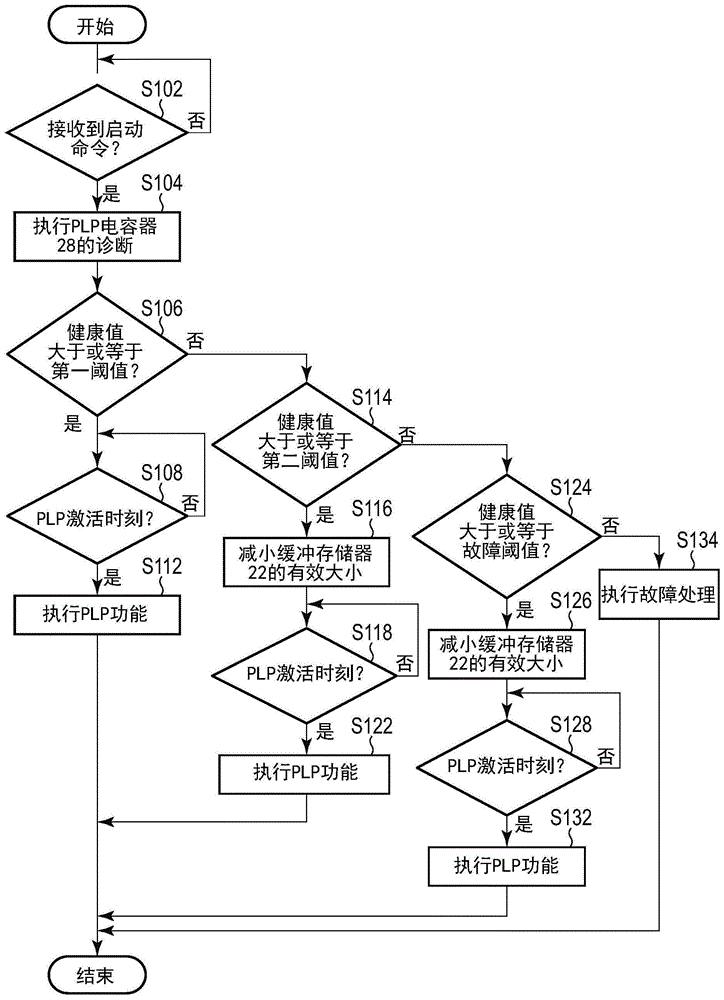
图13是示出根据第一实施方式,执行PLP功能的控制器的处理示例的流程图。FIG. 13 is a flowchart showing an example of processing of a controller executing a PLP function according to the first embodiment.
图14是示出根据第一实施方式,执行PLP功能的控制器的处理的另一示例的流程图。Fig. 14 is a flowchart showing another example of processing of the controller executing the PLP function according to the first embodiment.
图15是示出根据第二实施方式,执行PLP功能的控制器的处理示例的流程图。Fig. 15 is a flowchart showing an example of processing of a controller executing a PLP function according to the second embodiment.
图16是示出根据第三实施方式,执行PLP功能的控制器的处理示例的流程图。Fig. 16 is a flowchart showing an example of processing of a controller executing a PLP function according to the third embodiment.
图17是示出根据第四实施方式,执行PLP功能的控制器14的处理示例的流程图。FIG. 17 is a flowchart showing an example of processing by the
具体实施方式Detailed ways
下文将参照附图来描述各种实施方式。Various embodiments will be described below with reference to the accompanying drawings.
本公开内容仅仅是举例,其不受下面描述的实施方式中所描述的内容的限制。本领域普通技术人员容易想到的修改理所当然地落入本发明的保护范围。为了使描述更清楚起见,与精确表示中的大小、形状等相比,各部分的大小、形状等等可以在附图中进行改变并示意性地示出。多个附图中彼此对应的构成元件通过相同的附图标记来表示,并且除非必要,否则可以省略它们的详细描述。The present disclosure is only an example, and it is not limited by what is described in the embodiments described below. Modifications easily conceivable by those skilled in the art naturally fall within the protection scope of the present invention. For clarity of description, the size, shape, etc. of each part may be changed in the drawings and schematically shown compared with those in the exact representation. Constituent elements corresponding to each other in a plurality of drawings are denoted by the same reference numerals, and their detailed descriptions may be omitted unless necessary.
图1是示出根据第一实施方式的信息处理系统1的例子的框图。信息处理系统1包括存储系统4和可连接到存储系统4的主机设备(下文简称为主机)2。存储系统4是被配置为将数据写入非易失性存储器16和从非易失性存储器16读取数据的存储设备。在本说明书中,存储系统4例如是SSD。非易失性存储器的示例是NAND闪存、NOR闪存、磁阻随机存取存储器(MRAM)、相变随机存取存储器(PRAM)、电阻随机存取存储器(ReRAM)、铁电随机存取存储器(FeRAM)等。在本说明书中,非易失性存储器16例如是NAND闪存(以下简称为NAND存储器)。如上所述,信息处理系统1包括主机2和连接到主机2的SSD 4。FIG. 1 is a block diagram showing an example of an
主机2是用作访问SSD 4的外部设备的信息处理装置。主机2可以是在SSD 4中存储大量数据和多种数据的服务器(存储服务器)。主机2可以是个人计算机。SSD 4可以是组装到诸如数据中心的服务器中的用于商业用途的SSD。SSD 4可以是组装到个人计算机中的个人使用的SSD。The host computer 2 is an information processing device serving as an external device that accesses the SSD 4 . The host 2 may be a server (storage server) that stores a large amount of data and various kinds of data in the SSD 4 . Host 2 may be a personal computer. The SSD 4 may be an SSD for commercial use incorporated into a server such as a data center. The SSD 4 may be a personal use SSD incorporated into a personal computer.
SSD 4包括连接器12、控制器14、NAND存储器16、动态随机存取存储器(DRAM)20、电源电路24和包括多个电容器的备用电源电路30。SSD4可以作为主机2的主存储设备使用。SSD 4可以内置在主机2中,也可以设置在主机2的外部,或者通过电缆或网络与主机2连接。SSD 4 includes
控制器14根据从主机2发送的命令(请求),将数据写入NAND存储器16,并从NAND存储器16读取数据。此外,控制器14根据从主机2发送的命令和从电源电路24发送的各种信息,生成控制信号以控制由电源电路24产生的电压值。控制器14将产生的控制信号发送给电源电路24。当接收到该控制信号时,控制器14控制提供给SSD 4的每个设备(例如,NAND存储器16、控制器14和DRAM 20)的电压。此外,控制器14还控制PLP功能的执行。控制器14可以由诸如片上系统(SoC)之类的电路来构成。The
电源电路24从外部提供的单个电压或多个电压,产生SSD 4的各设备所需要的电压。从外部提供的电压的电源可以是内部电源,也可以是外部电源。外部电源可以是主机2的电源。在图1中,电源是主机2的电源,但在图中没有显示电源线。电源电路24还可以从备用电源电路30提供的电压,产生SSD 4的各设备所需的电压。电源电路24可以是单个集成电路(IC)或多个IC。根据规定的通信标准,将表示电源电路24的各种状态的信息发送到控制器14。规定的通信标准可以是串行通信标准。串行通信标准的示例之一是I2C格式。在本说明书中,假设电源电路24和控制器14之间的通信标准基于I2C格式。A single voltage or a plurality of voltages supplied from the outside by the
DRAM 20是易失性存储器的例子。例如,DRAM 20是双倍数据速率3低压(DDR3L)标准的DRAM。DRAM 20包括缓冲存储器22。缓冲存储器22包括写缓冲器22a、读缓冲器22b和管理信息缓冲器22c。从主机2提供给SSD 4的、正在向NAND存储器16写入途中的或尚未写入NAND存储器16的数据存储在写缓冲器22a中。从NAND存储器16读取的、正在向主机2传输的或尚未传输到主机2的数据存储在读缓冲器22b中。查找表、在SSD 4的操作期间使用的各种表、以及各种值,存储在管理信息缓冲器22c中。各种值的示例之一是其数据已经通过PLP功能写入NAND存储器16的块的地址,即,非易失性块的地址。查找表表示主机2指定的逻辑地址和NAND存储器16的物理地址之间的对应关系。
作为易失性存储器的DRAM 20不仅可以设置在控制器14的外部,也可以设置在控制器14的内部。作为易失性存储器,可以使用能够进行更快访问的静态随机存取存储器(SRAM)来代替DRAM 20。The
NAND存储器16可以包括多个(例如,十六个)NAND芯片18。NAND芯片18中的每一个可以包括存储单元阵列,该存储单元阵列包括以矩阵排列的多个存储单元。NAND芯片18可以由具有二维结构的存储单元阵列来形成,或者由具有三维结构的存储单元阵列来形成。
存储单元阵列包括多个块(block)。这些块中的每一个块包括多个页(page)。这些块用作数据擦除操作的单位。所述多个页中的每一个页包括连接到同一字线的多个存储单元。页是数据写入操作和数据读取操作的单位。The memory cell array includes a plurality of blocks. Each of these blocks includes a plurality of pages. These blocks are used as the unit of data erase operation. Each of the plurality of pages includes a plurality of memory cells connected to the same word line. A page is a unit of data write operation and data read operation.
将一页的数据作为写入单位的数据存储在写缓冲器22a中,或者作为读取单位的数据存储在读缓冲器22b中。在写入时,将从写缓冲器22a读取的一页的写入单位的数据写入NAND存储器16。当不是因为发出关机命令而导致的电源切断,而是发生意外的电源切断时,并且电源电路24没有在写入过程中产生电压,则写缓冲器22a中正在写入或未写入NAND存储器16的数据将丢失。此时,类似于写缓冲器22a中的数据,读缓冲器22b和管理信息缓冲器22c中的数据也丢失。如果SSD 4接收到关机命令,则控制器14将缓冲存储器22中的数据写入NAND存储器16,然后停止电源电路24的操作。Data of one page is stored in the
在第一实施方式中,设置了备用电源电路30。在意外的电源切断时,控制器14可以通过使用备用电源电路30,将缓冲存储器22中的数据写入NAND存储器16。In the first embodiment, a backup
控制器14根据从主机2发送的命令(请求)和从电源电路24发送的各种信息,产生控制信号来控制电源电路24产生的电压值。控制器14向电源电路24发送所产生的控制信号。因此,提供给SSD 4的各设备的多个电压由控制器14进行控制。The
备用电源电路30连接到电源电路24。当不是由关机命令引起的电源切断,而是发生意外的电源切断时,备用电源电路30向电源电路24提供电压以保护正在写入或未写入NAND存储器16中的数据。备用电源电路30由并联连接的多个PLP电容器构成。将在后面参考图3来描述PLP电容器。PLP电容器的例子包括双电层电容器、导电性聚合物铝电解电容器、导电性聚合物钽固体电解电容器等等。A
电源电路24包括PLP功能,其在不是由关机命令引起的电源切断而是发生意外的电源切断的情况下,也能通过使用从备用电源电路30馈送的供电能力在一定时间段内继续向NAND存储器16、控制器14和DRAM 20提供电压。当发生意外的电源切断时,控制器14向电源电路24发送执行PLP功能的命令。The
供电能力对应于备用电源电路30中包含的多个PLP电容器所蓄积的合成静电电容(总电容)。根据电源电路24在电源切断之后,向NAND存储器16、控制器14和DRAM 20提供电压以执行PLP功能的时间(备用时间),来设置合成静电电容。将该合成静电电容(下文有时简称为PLP电容器的静电电容)设置为比以下静电电容稍大,即:使得在该电压供给时间完成将存储在缓冲存储器22中的正在向NAND存储器16写入中途的数据完成向NAND存储器16的写入,即,完成非易失化的静电电容。这是因为,通过在PLP电容器的静电电容中设置余量,可以在该电压供给时间内完成缓冲存储器22中存储的数据的非易失化,即,即使PLP电容器的静电电容由于老化退化等而略微减小,也可以实现PLP功能。The power supply capability corresponds to the combined electrostatic capacitance (total capacitance) accumulated in the plurality of PLP capacitors included in the backup
控制器14包括CPU 32、主机接口(主机I/F)电路34、NAND接口(NAND I/F)电路36和DRAM接口(DRAM I/F)电路38。CPU 32、主机I/F电路34、NAND I/F电路36、DRAM I/F电路38连接到总线40。虽然没有直接示出,但电源电路24也连接到总线40。The
CPU 32执行存储在NAND存储器16中的固件以实现各种功能。各种功能的示例包括备用电源电路30的充电控制和使用电源电路24的PLP功能的控制。The
主机I/F电路34通过连接器12电连接到主机2。NAND I/F电路36电连接到NAND存储器16。DRAM I/F电路38电连接到DRAM 20。The host I/
将主机2电连接到SSD 4的主机I/F电路34,符合诸如小型计算机系统接口(SCSI)、串行连接SCSI(SAS)、AT附件(ATA)、串行ATA(SATA)等标准、PCI Express(PCIe)TM、EthernetTM、Fibre channel TM、NVM Express(NVMe)TM、通用串行总线(USB)TM和通用异步接收器/发送器(UART)TM之类的标准。The host I/
将控制器14和NAND存储器16电互连的NAND I/F电路36,符合诸如Toggle DDR和开放式NAND闪存接口(ONFI)之类的标准。NAND I/F电路36经由多个(例如,18个)通道连接到NAND存储器16。NAND I/
图2是示出根据第一实施方式的SSD 4的外观示例的平面图。将SSD 4设置在外壳44中。在外壳44的一端设置有凹口(notch)46。在凹口46中设置有连接器12。连接器12包括多个引脚12a,其包括信号引脚和电源引脚。外壳44包括上外壳44a和下外壳(没有示出)。上外壳44a和下外壳通过螺钉来实现一体化。FIG. 2 is a plan view showing an example of the appearance of the SSD 4 according to the first embodiment. SSD 4 is disposed in
图3A和3B是示出根据第一实施方式的SSD 4的构成部件布置示例的平面图。图3A示出了SSD 4的衬底52的表面(即,与上外壳44a相对的表面)。衬底52的形状是具有四个边52a、52b、52c和52d的矩形。在短边的一侧52a上设置连接器12。将连接器12的引脚12a设置在衬底52的表面上。将控制器14、DRAM 20、电源电路24和备用电源电路30设置在衬底52的表面上。图3B示出了衬底52的背面(即,与下外壳相对的表面)。将NAND芯片18设置在衬底52的背面。3A and 3B are plan views showing an example of the arrangement of constituent parts of the SSD 4 according to the first embodiment. FIG. 3A shows the surface of the
由于控制器14处理经由连接器12输入或输出的高速信号,因此控制器14布置在连接器12附近。具体地说,控制器14布置在连接各个长边52c和52d的中点的线以及连接器12侧的短边52a之间。将DRAM 20设置在控制器14附近。Since the
构成备用电源电路30的PLP电容器28集中布置在连接衬底52的各长边52c、52d的中点的线和与连接器12相对的短边52b之间。控制器14是衬底52上的元件的最大热源。PLP电容器28因热而劣化,但是,由于将PLP电容器28布置成与控制器14尽可能地分离,因此由热引起的劣化减到最小。The
与PLP电容器28类似,NAND芯片18具有低耐热性。将NAND芯片18设置在与设置有控制器14和PLP电容器28的面相反的面上。例如,NAND芯片18集中布置在连接衬底52的各长边52c、52d的中点的线和与连接器12相反的短边52b之间。因此,由于将NAND芯片18布置为尽可能远离控制器14,因此防止了NAND芯片18受到热影响。Similar to the
与控制器14相比,NAND芯片18对PLP电容器28的影响较小,但会产生一些热量。如附图中所示,PLP电容器28优选地设置在与NAND芯片18分离的位置。即使如此考虑SSD 4中的构成部件之间的热效应来执行布局设计,PLP电容器28也可能由于其它外部因素等等而劣化,并且PLP功能可能无法正常操作。因此,本实施方式包括如下面详细描述的电源系统。The
图4是示出包括根据第一实施方式的电源电路24、包括PLP电容器28的备用电源电路30、以及健康值测量电路74的电源系统的配置示例的框图。4 is a block diagram showing a configuration example of a power supply system including the
电源电路24包括熔断器62、负载开关64、低压差(LDO)稳压器66、DC/DC转换器68、控制逻辑70、I2C I/F电路72和A/D转换器(A/D)76。电源(没有示出)产生电压,例如,DC12V的电压。通过熔断器62和负载开关64,串联地向LDO稳压器66和DC/DC转换器68提供与电压相对应的大小的电流。主机2可以包括电源,可以从主机2向电源电路24提供与电压相对应的电流。构成电源电路24的单个IC或多个IC可以称为电源管理集成电路(PMIC)。
熔断器62由金属熔断器构成,当熔断器62流过一定电流以上的过电流时发生熔断。当熔断器62熔断时,除非更换熔断器,否则不向负载开关64提供电压。熔断器62并不限于金属熔断器,也可以由在检测到过电流时变为非导通的电子熔断器形成。The
负载开关64是通断开关,其通常处于接通状态。在接通状态下,负载开关64输出通过从供给电压中减去压差(dropout)电压而获得的电压。与熔断器62相同,负载开关64在流过一定电流以上的过电流时变成断开状态。在断开状态下,负载开关64输出0V。熔断器62熔断时的过电流值可以高于、低于或等于负载开关64从接通状态变为断开状态时的过电流值。通过熔断器62和负载开关64以双重方式防止向LDO稳压器66和DC/DC转换器68提供过电流。
LDO稳压器66是用于产生需要小电流的SSD 4的一个(或多个)器件的一个电压(或多个电压)的电路。DC/DC转换器68是用于产生需要大电流的SSD 4的一个(或多个)器件的一个电压(或多个电压)的电路。LDO稳压器66可以由独立的IC或单个IC形成。DC/DC转换器68也可以由独立的IC或单个IC形成。
LDO稳压器66降低负载开关64的电压输出。将LDO稳压器66的电压输出提供给控制器14。
DC/DC转换器68对负载开关64的输出电压进行升压或降压,以产生SSD 4中的各设备(控制器14、NAND存储器16、DRAM 20等)所需的一个电压(或多个电压)。DC/DC转换器68由分别对多个电压进行升压或降压的多个DC/DC转换器单元构成。The DC/
升压DC/DC转换器单元对负载开关64的输出电压进行升压,并将升压后的电压作为充电电压提供给并联连接的多个PLP电容器28。所述多个PLP电容器28构成备用电源电路30。The step-up DC/DC converter unit boosts the output voltage of the
降压DC/DC转换器单元通过对负载开关64的输出电压进行降压来分别产生多个电压。降压DC/DC转换器单元产生的电压提供给NAND存储器16、DRAM 20和控制器14。The step-down DC/DC converter unit generates a plurality of voltages respectively by stepping down the output voltage of the
控制逻辑70监测负载开关64的输出电压。当检测到输出电压已经下降到规定电压(例如,0V时),控制逻辑70向控制器14发送检测结果。即使控制器14没有接收到关机命令,当通知控制器14负载开关64的输出电压已变为0V时,控制器14确定发生了不是由关机引起的意外的电源切断,并向控制逻辑70发送PLP命令。
当接收到PLP命令时,控制逻辑70使PLP电容器28充电的电压(输出电压)输入到DC/DC转换器68中的降压DC/DC转换器单元。结果,在电源意外切断后的一段时间内,降压DC/DC转换器单元将PLP电容器28的输出电压降压,并将降压电压提供给NAND存储器16、DRAM 20和控制器14,还向LDO稳压器66提供降压电压。结果,在电源意外切断后的一段时间,DC/DC转换器68和LDO稳压器66可以将通过对PLP电容器28的输出电压进行降压而产生的电压(或多个电压)提供给NAND存储器16、DRAM 20和控制器14。通过使用PLP电容器28的输出电压而实现了PLP功能,即,缓冲存储器22中的数据被写入NAND存储器16,也就是,非易失化。When a PLP command is received, the
I2C I/F电路72连接到控制逻辑70和控制器14的总线40,以便响应于从控制逻辑70发送的控制信号与控制器14进行通信。通过I2C I/F电路72,将来自控制器14的控制信号提供给控制逻辑70。I2C I/
健康值测量电路74与多个PLP电容器28并联连接。健康值测量电路74对并联连接的PLP电容器28蓄积的合成静电电容(总电容)进行测量,并将测量结果作为PLP电容器28的健康值进行输出。健康值表示从备用电源电路30馈送的供电能力。健康值对应于PLP电容器28可以输出电压以实现PLP功能的时间。换言之,健康值对应于PLP电容器28的输出电压可以写入NAND存储器16的数据的大小。如果健康值高于或等于阈值,则确定可以实现PLP功能。如果健康值低于阈值,则确定无法实现PLP功能并且SSD 4发生故障。健康值测量电路74以固定周期测量并输出健康值。从健康值测量电路74输出的健康值经由A/D 76提供给控制逻辑70。The health
以下将描述PLP功能。The PLP function will be described below.
首先,将描述比较例的PLP功能。比较例的硬件配置与图1至图4所示的第一实施方式的硬件配置相同。与PLP功能相关的控制器14的控制操作与第一实施方式的不同。First, the PLP function of the comparative example will be described. The hardware configuration of the comparative example is the same as that of the first embodiment shown in FIGS. 1 to 4 . The control operation of the
在比较例中,将单个故障阈值设置为用于确定PLP电容器28的劣化的健康值或供电能力的阈值。根据可以存储在缓冲存储器22中并且可以通过PLP功能写入NAND存储器16的PLP对象数据的大小,来设置故障阈值。该大小可以称为缓冲存储器16的数据可存储大小。当PLP电容器28劣化时,在一些情况下,通常不能将PLP电容器28充电到将缓冲存储器22中存储的所有PLP对象数据写入到NAND存储器16所需的规定电压。为了预测PLP电容器28不能用作PLP电容器,控制器14将健康值测量电路74测量的PLP电容器28的健康值与故障阈值进行比较。In the comparative example, a single failure threshold was set as the threshold for determining the degraded health value or power supply capability of the
图5是示出PLP电容器28的健康值等于或大于故障阈值的情况下的比较例的PLP功能的视图。在这种情况下,PLP电容器28的输出电压可以写入NAND存储器16的数据的大小,大于缓冲存储器22中存储的PLP对象数据102的大小。可以通过PLP功能,将所有PLP对象数据102写入NAND存储器16。FIG. 5 is a view showing the PLP function of the comparative example in the case where the health value of the
图6是示出健康值小于故障阈值的情况下的比较例的PLP功能的视图。在这种情况下,可以通过PLP电容器28的输出电压写入NAND存储器16的数据的大小,小于缓冲存储器22中存储的PLP对象数据106的大小。可以通过PLP功能,将PLP对象数据106中的部分106a(与健康值对应的部分106a)写入NAND存储器16,但PLP对象数据106的剩余部分106b不能通过PLP功能写入NAND存储器16(非易失化失败),故认为SSD 4发生故障。FIG. 6 is a view showing a PLP function of a comparative example in a case where a health value is smaller than a failure threshold. In this case, the size of data that can be written into the
因此,在比较例中,当健康值小于故障阈值时,认为SSD 4发生故障。Therefore, in the comparative example, when the health value is smaller than the failure threshold, it is considered that the SSD 4 has failed.
接下来,将描述由第一实施方式的SSD 4提供的PLP功能。在第一实施方式中,将故障阈值和大于故障阈值的至少一个值设置为健康值或供电能力的阈值,以用于确定PLP电容器28的劣化。设置两个值,即大于故障阈值的第二阈值和大于第二阈值的第一阈值。然而,可以仅将第一阈值设置为故障阈值以外的值,或者可以将三个或更多阈值设置为不是故障阈值。在比较例中,健康值的阈值仅为一个故障阈值,可以存储在缓冲存储器22中的PLP对象数据的大小是固定的。然而,在第一实施方式中,设置了多个阈值,并且PLP对象数据的大小(或者称为缓冲存储器22的有效大小)是可变的。缓冲存储器22的有效大小是可以存储数据的缓冲存储器22的最大可存储大小的大小。存储在缓冲存储器16中的数据包括从主机2发送到SSD 4的数据、用于用户数据的日志数据、用于ECC的数据、与查找表相关的数据等等。缓冲存储器22并不限于物理存储器,也可以通过逻辑(虚拟)缓冲器来实现。Next, the PLP function provided by the SSD 4 of the first embodiment will be described. In the first embodiment, the failure threshold and at least one value greater than the failure threshold are set as health values or thresholds of power supply capability for determining degradation of the
控制器14控制缓冲存储器22的写入,使得存储在缓冲存储器22中的数据的大小不会大于或等于有效大小。例如,当存储在缓冲存储器22中的数据的大小可能变得大于有效大小时,控制器14将存储在缓冲存储器22中的数据的一部分写入NAND存储器16,然后通过删除该部分数据来减少存储在缓冲存储器22中的数据的大小。The
最初,控制器14将缓冲存储器22的有效大小设置为与大于或等于第一阈值的健康值相对应的大小。控制器14将健康值测量电路74测量的PLP电容器28的健康值与第一阈值进行比较。Initially, the
图7是示出在健康值大于或等于第一阈值的情况下,根据第一实施方式的SSD 4的PLP功能的视图。在这种情况下,PLP电容器28的输出电压可以写入NAND存储器16的数据的大小,大于缓冲存储器22中存储的PLP对象数据112的大小。可以通过PLP功能将所有PLP对象数据112写入NAND存储器16,并且PLP功能正常运行。FIG. 7 is a view showing the PLP function of the SSD 4 according to the first embodiment in a case where the health value is greater than or equal to the first threshold. In this case, the output voltage of the
图8是示出健康值小于第一阈值并且大于或等于第二阈值的情况下,根据第一实施方式的SSD 4的PLP功能的视图。在这种情况下,可以通过PLP电容器28的输出电压写入NAND存储器16的数据的大小,小于存储在缓冲存储器22中的PLP对象数据114的大小。不能通过PLP功能,将所有PLP对象数据114写入NAND存储器16。控制器14将缓冲存储器22的有效大小,从与第一阈值相对应的大小改变为与第二阈值相对应的大小。也就是说,控制器14减小缓冲存储器22的有效大小。通过这种减小,也将PLP对象数据114减少为作为其一部分的PLP对象数据114a。结果,可以通过PLP电容器28的输出电压写入NAND存储器16的数据的大小,变得大于减小后的PLP对象数据114a的大小。可以将所有PLP对象数据114a都写入NAND存储器16中。FIG. 8 is a view showing the PLP function of the SSD 4 according to the first embodiment in the case where the health value is less than the first threshold and greater than or equal to the second threshold. In this case, the size of data that can be written into the
在缓冲存储器22的有效大小被减小之前,控制器14将数据114b也就是PLP对象数据114和减小后的PLP对象数据114a之间的差写入NAND存储器16中。要写入NAND存储器16的差数据的示例是存储在写缓冲器22a中的数据,该数据正在写入NAND存储器16或者未写入NAND存储器16。替代地,该差数据的例子是写入缓冲存储器22的数据中的特定大小的数据,其包括写入缓冲存储器22的最新数据。Before the effective size of the
图9是示出在健康值小于第一阈值并且大于或等于第二阈值的情况下,根据第一实施方式的SSD 4的PLP功能的视图。在这种情况下,PLP电容器28的输出电压可以写入NAND存储器16的数据的大小,大于缓冲存储器22中存储的PLP对象数据118的大小。可以通过PLP功能将所有PLP对象数据118写入NAND存储器16,并且PLP功能正常运行。FIG. 9 is a view showing the PLP function of the SSD 4 according to the first embodiment in a case where the health value is less than the first threshold and greater than or equal to the second threshold. In this case, the output voltage of the
图10是示出在健康值小于第二阈值并且大于或等于故障阈值的情况下,根据第一实施方式的SSD 4的PLP功能的视图。在这种情况下,可以通过PLP电容器28的输出电压写入NAND存储器16的数据的大小,小于存储在缓冲存储器22中的PLP对象数据122的大小。不能通过PLP功能将所有PLP对象数据122写入NAND存储器16。控制器14将缓冲存储器22的有效大小从与第二阈值相对应的大小改变为与故障阈值相对应的大小。也就是说,控制器14减小缓冲存储器22的有效大小。通过该减小,还将PLP对象数据122减少为作为其一部分的PLP对象数据122a。结果,可以通过PLP电容器28的输出电压写入NAND存储器16的数据的大小变得大于减小后的PLP对象数据122a的大小。可以将所有PLP对象数据122a都写入NAND存储器16中。FIG. 10 is a view showing the PLP function of the SSD 4 according to the first embodiment in the case where the health value is less than the second threshold and greater than or equal to the failure threshold. In this case, the size of data that can be written into the
在缓冲存储器22的有效大小被减小之前,控制器14将数据122b也就是PLP对象数据122和减小后的PLP对象数据122a之间的差写入NAND存储器16。要写入NAND存储器16的差数据的示例是存储在写缓冲器22a中的数据,该数据正在写入NAND存储器16或者未写入NAND存储器16。替代地,该差数据的例子是写入缓冲存储器22的数据中的特定大小的数据,其包括写入缓冲存储器22的最新数据。Before the effective size of the
图11是示出在健康值小于第二阈值并且大于或等于故障阈值的情况下,根据第一实施方式的SSD 4的PLP功能的视图。在这种情况下,可以通过PLP电容器28的输出电压写入NAND存储器16的数据的大小,大于缓冲存储器22中存储的PLP对象数据126的大小。可以通过PLP功能将所有PLP对象数据126写入NAND存储器16,并且PLP功能正常运行。FIG. 11 is a view showing the PLP function of the SSD 4 according to the first embodiment in a case where the health value is less than the second threshold and greater than or equal to the failure threshold. In this case, the size of data that can be written into the
图12是示出在健康值小于故障阈值的情况下,根据第一实施方式的SSD 4的PLP功能的视图。在这种情况下,可以通过PLP电容器28的输出电压写入NAND存储器16的数据的大小,小于存储在缓冲存储器22中的PLP对象数据128的大小。可以通过PLP功能,将PLP对象数据128的一部分128a(与健康值相对应的部分128a)写入NAND存储器16,但不能通过PLP功能将剩余部分128b写入NAND存储器16(非易失化失败),PLP功能无法正常运行,故认为SSD 4发生故障。FIG. 12 is a view showing the PLP function of the SSD 4 according to the first embodiment in a case where the health value is smaller than the failure threshold. In this case, the size of data that can be written into the
图13是示出根据图7至图12中所示的第一实施方式,控制器14执行SSD 4的PLP功能的处理示例的流程图。FIG. 13 is a flowchart showing an example of processing in which the
在步骤S102中,控制器14判断该控制器14是否接收到来自主机20的启动命令。控制器14重复步骤S102的判断,直到控制器14接收到启动命令为止。DDS 4可以设置第一阈值、第二阈值和故障阈值。替代地,主机2可以设置这些阈值。当主机2在SSD 4中设置这些阈值时,主机2可以将启动命令与表示阈值的信息一起发送到SSD 4。In step S102 , the
当接收到启动命令时(S102中的是),控制器14在步骤S104中执行PLP电容器28的诊断。具体地说,控制器14接收健康值测量电路74所测量的健康值。When the start command is received (YES in S102), the
在步骤S106中,控制器14判断健康值是否大于或等于第一阈值。当健康值大于或等于第一阈值时(S106中的是),控制器14在步骤S108中判断PLP激活时刻是否已经到来。当控制逻辑70通知控制器14负载开关64的输出电压已经变为0V时,即使控制器14没有接收到关机命令,控制器14也确定PLP激活时刻已经到来。In step S106, the
控制器14重复步骤S108的确定,直到PLP激活时刻到来为止。当PLP激活时刻到来时(S108中的是),控制器14在步骤S112中执行PLP功能。在这种情况下,所有的PLP对象数据112被非易失化,如图7中所示。The
当在步骤S106中确定健康值小于第一阈值时(S106中的否),控制器14在步骤S114中判断健康值是否大于或等于第二阈值。当健康值大于或等于第二阈值时(S114中的是),控制器14在步骤S116中将缓冲存储器22的有效大小减小到与第二阈值相对应的大小,如图8中所示,这是由于健康值小于第一阈值并且大于或等于第二阈值。When it is determined in step S106 that the health value is less than the first threshold (NO in S106), the
在步骤S118中,控制器14判断PLP激活时刻是否到来。控制器14重复步骤S118的确定,直到PLP激活时刻到来为止。当PLP激活时刻到来时(S118中的是),控制器14在步骤S122中执行PLP功能。在这种情况下,所有PLP对象数据118都被非易失化,如图9中所示。In step S118, the
当在步骤S114中确定健康值小于第二阈值时(S114中的否),控制器14在步骤S124中判断健康值是否大于或等于故障阈值。当健康值大于或等于故障阈值时(S124中的是),健康值小于第二阈值并且大于或等于故障阈值,因此控制器14在步骤S126中,将缓冲存储器22的有效大小缩小为与故障阈值相对应的大小,如图10中所示。When it is determined in step S114 that the health value is less than the second threshold (NO in S114 ), the
在步骤S128中,控制器14判断PLP激活时刻是否到来。控制器14重复步骤S128的确定,直到PLP激活时刻到来为止。当PLP激活时刻到来时(S128中的是),控制器14在步骤S132中执行PLP功能。在这种情况下,所有的PLP对象数据126都被非易失化,如图11中所示。In step S128, the
当在步骤S124中确定健康值小于故障阈值时(S124中的否),控制器14在步骤S134中执行故障处理。作为故障处理的示例,控制器14可以通知主机2由于PLP电容器28的性能劣化(即,SSD 4发生故障),PLP功能不能正常工作。When it is determined in step S124 that the health value is smaller than the failure threshold (NO in S124), the
图14是示出根据图7至图12中所示的第一实施方式,控制器14执行SSD 4的PLP功能的另一个处理示例的流程图。FIG. 14 is a flowchart showing another processing example in which the
在步骤S152中,控制器14判断该控制器14是否接收到来自主机20的关机命令。控制器14重复步骤S152的判断,直到控制器14接收到关机命令为止。主机2可以向SSD 4发送关机命令,其中包含表示第一阈值、第二阈值和故障阈值的信息。In step S152 , the
当接收到关机命令时(S152中的是),控制器14在步骤S154中执行PLP电容器28的诊断。此后,控制器14在步骤S106中判断健康值是否大于或等于第一阈值,类似于图13中所示的处理。在此之后,缓冲存储器22的有效大小根据情况而发生变更。变更后的有效大小永久地存储在NAND存储器16中。When receiving the shutdown command (YES in S152), the
图13示出了启动(boot)时执行PLP电容器28的诊断的例子,图14示出了在关机时执行PLP电容器28的诊断的例子。可以在这些时间以外的时间执行PLP电容器28的诊断和缓冲存储器22的有效大小的变更。例如,可以在主机2的命令处理不频繁时,或定期地执行该诊断。FIG. 13 shows an example of performing diagnosis of the
根据第一实施方式,即使当PLP电容器28的性能劣化并且PLP电容器28的合成静电电容减小时,控制器14也不会立即确定PLP功能将不正常工作,而是设置为减小缓冲存储器22的有效大小(即,PLP对象数据大小),以继续PLP功能的操作。通过减小缓冲存储器22的有效大小,等待缓冲存储器22具有与要写入的数据的大小相对应的足够可用空间的频度变高,将缓冲存储器22中的数据写入NAND存储器16的SSD 4的内部处理的执行频度也变高。因此SSD 4对来自主机2的命令的处理能力有所降低,但是PLP功能停止和SSD 4最终失败的时间可以延迟。也就是说,SSD 4的运行周期可以延长。According to the first embodiment, even when the performance of the
图15是示出根据第二实施方式,控制器14执行PLP功能的处理示例的流程图。第二实施方式的硬件配置与图1至图4中所示的第一实施方式的硬件配置相同。与PLP功能相关的控制器14的控制操作与第一实施方式的不同。FIG. 15 is a flowchart showing an example of processing by the
在步骤S202中,控制器14判断该控制器14是否接收到来自主机20的启动命令。控制器14重复步骤S102的判断,直到控制器14接收到启动命令为止。主机2可以向SSD 4发送启动命令,其中包含表示第一阈值、第二阈值和故障阈值的信息。In step S202 , the
当接收到启动命令时(S202中的是),控制器14在步骤S204中执行PLP电容器28的诊断。When the start command is received (YES in S202), the
在步骤S206中,控制器14判断该控制器14是否已经从主机20接收到PLP模式指定命令。在第二实施方式中,其中健康值的阈值仅为在比较例中设置的故障阈值的单阈值模式、以及其中健康值的阈值包括除在第一实施方式中设置的故障阈值之外的至少一个阈值的多阈值模式,被设置为PLP模式。在向SSD 4发送启动命令之后,主机2发送PLP模式指定命令以指定单阈值模式或多阈值模式。控制器14重复步骤S206的判断,直到控制器14接收到PLP模式指定命令为止。In step S206 , the
当接收到PLP模式指定命令时(S206中的是),控制器14在步骤S208中判断PLP模式指定命令是指定单阈值模式还是多阈值模式。当指定多阈值模式时,控制器14在步骤S106中判断健康值是否大于或等于第一阈值,类似于第一实施方式。之后,在某些情况下变更缓冲存储器22的有效大小。When the PLP mode designation command is received (YES in S206), the
当指定单一阈值模式时,控制器14在步骤S212中,判断健康值是否大于或等于故障阈值。当健康值大于或等于故障阈值时(S212中的是),控制器14判断PLP激活时刻是否已经到来。控制器14重复步骤S214的判断,直到PLP激活时刻到来为止。当PLP激活时刻到来时(S214中的是),控制器14在步骤S216中执行PLP功能。在这种情况下,所有的PLP对象数据102都被非易失化,如图5中所示。将单阈值模式的故障阈值设置为与多阈值模式的故障阈值不同的值。例如,可以将单阈值模式的故障阈值设置为多阈值模式的第一阈值。When the single threshold mode is specified, the
当在步骤S212中确定健康值小于故障阈值时(S212中的否),控制器14在步骤S218中执行故障处理。When it is determined in step S212 that the health value is smaller than the failure threshold (NO in S212), the
主机2可以在关机命令之后发送PLP模式指定命令,在主机2处理较少命令时发送该命令,或者以固定间隔发送该命令。The host 2 may send the PLP mode specifying command after the shutdown command, send the command when the host 2 processes fewer commands, or send the command at fixed intervals.
根据第二实施方式,作为PLP模式,SSD 4具备具有用于确定PLP功能故障的PLP电容器28的健康值的单一阈值的单一阈值模式和具有多个阈值的多阈值模式,主机2可以选择PLP模式。According to the second embodiment, as the PLP mode, the SSD 4 is equipped with a single threshold mode having a single threshold for determining the health value of the
图16是示出根据第三实施方式,控制器14执行PLP功能的处理示例的流程图。第三实施方式的硬件配置与图1至图4所示的第一实施方式的硬件配置相同。与PLP功能相关的控制器14的控制操作与第一实施方式的不同。在图16的流程图中,通过相同的附图标记来表示与图13的处理相同的处理。FIG. 16 is a flowchart showing an example of processing in which the
控制器14接收启动指令(步骤S102),执行PLP电容器28的诊断(步骤104),并判断健康值是否大于或等于第一阈值(步骤S106)。The
当健康值小于第一阈值时(S106中的否),控制器14判断健康值是否大于或等于第二阈值(步骤S114)。When the health value is less than the first threshold (No in S106), the
当健康值大于或等于第二阈值时(S114中的是),控制器14在步骤S116中,将缓冲存储器22的有效大小减小到与第二阈值相对应的大小。在步骤S302中,控制器14向主机2发送表示PLP电容器28的健康值和缓冲存储器22的减小后的有效大小中的至少一个的信息。在步骤S118中,控制器14判断PLP激活时刻是否到来。When the health value is greater than or equal to the second threshold (Yes in S114), the
当健康值小于第二阈值时(S114中的否),控制器判断健康值是否大于或等于故障阈值(步骤S124)。当健康值大于或等于故障阈值时(S124中的是),控制器14在步骤S126中,将缓冲存储器22的有效大小减小到与故障阈值相对应的大小。在步骤S304中,控制器14向主机2发送表示PLP电容器28的健康值和缓冲存储器22的减小后的有效大小中的至少一个的信息。在步骤S128中,控制器14判断PLP激活时刻是否到来。When the health value is less than the second threshold (No in S114), the controller judges whether the health value is greater than or equal to the failure threshold (step S124). When the health value is greater than or equal to the failure threshold (Yes in S124), the
当健康值小于故障阈值时(S124中的否),控制器14在步骤S134中执行故障处理。When the health value is smaller than the failure threshold (NO in S124), the
根据第三实施方式,主机2可以接收表示PLP电容器28的健康值和缓冲存储器22的减小后的有效大小中的至少一个的信息。主机2可以根据PLP电容器28的健康值的变化,来预测SSD 4由于PLP功能的故障而发生故障之前的时间。替代地,主机2可以根据缓冲存储器22的有效大小的减小率(=(C-B)/C),来预测SSD 4由于PLP功能的故障而发生故障之前的时间,其中C是缓冲存储器22的有效大小的初始值,B是缓冲存储器22的减小后的有效大小。According to the third embodiment, the host 2 may receive information indicative of at least one of the health value of the
在第一实施方式中已经描述了在接收到关机命令之后执行PLP电容器28的诊断的修改示例(图14)。在第三实施方式中,也可以在接收到关机命令之后执行PLP电容器28的诊断。在这种情况下,控制器14在接收到关机命令并在诊断PLP电容器28之后,向主机2发送表示PLP电容器28的健康值和缓冲存储器22的减小后有效大小中的至少一个的信息。A modified example in which the diagnosis of the
图17是根据第四实施方式,示出控制器14执行PLP功能的处理示例的流程图。第四实施方式的硬件配置与图1至图4中所示的第一实施方式的硬件配置相同。与PLP功能相关的控制器14的控制操作与第一实施方式的不同。FIG. 17 is a flowchart showing an example of processing by the
在步骤S312中,控制器14判断控制器14是否已经从主机20接收到通知请求命令。控制器14执行其它处理的同时在后台执行步骤S312的判断。当主机20从控制器14要求表示PLP电容器28的健康值和缓冲存储器22的减小的有效大小中的至少一个的信息时,主机20向控制器14发送通知请求命令。控制器14重复步骤S132的判断,直到控制器14接收到通知请求命令为止。In step S312 , the
当接收到通知请求命令时(S312中的是),控制器14在步骤S314中执行PLP电容器28的诊断。When receiving the notification request command (YES in S312), the
在步骤S316中,控制器14向主机2发送表示PLP电容器28的健康值和缓冲存储器22的有效大小中的至少一个的信息。In step S316 , the
根据第四实施方式,主机2可以在所需的时间,接收表示PLP电容器28的健康值和缓冲存储器22的有效大小中的至少一个的信息。According to the fourth embodiment, the host computer 2 can receive information indicating at least one of the health value of the
尽管已经描述了某些实施方式,但仅以示例的方式呈现这些实施方式,它们并不旨在限制本发明的范围。实际上,本文所描述的新颖实施方式可以以多种其它形式来体现;此外,在不脱离本发明的精神的情况下,可以对本文描述的实施方式的形式进行各种省略、替换和改变。所附权利要求及其等同物旨在覆盖落入本发明的保护范围和精神内的这些形式或修改。While certain embodiments have been described, these embodiments have been presented by way of example only, and they are not intended to limit the scope of the inventions. Indeed, the novel embodiments described herein may be embodied in many other forms; moreover, various omissions, substitutions and changes in the form of the embodiments described herein may be made without departing from the spirit of the inventions. The appended claims and their equivalents are intended to cover such forms or modifications as fall within the scope and spirit of the invention.
附图标记:Reference signs:
2:主机2: Host
4:SSD4: SSD
14:控制器14: Controller
16:NAND存储器16: NAND memory
22:缓冲存储器22: buffer memory
24:电源电路24: Power circuit
30:备用电源电路30: Backup power circuit
Claims (22)
Applications Claiming Priority (2)
| Application Number | Priority Date | Filing Date | Title |
|---|---|---|---|
| JP2021149340A JP2023042175A (en) | 2021-09-14 | 2021-09-14 | Memory system and method for controlling memory system |
| JP2021-149340 | 2021-09-14 |
Publications (1)
| Publication Number | Publication Date |
|---|---|
| CN115810369A true CN115810369A (en) | 2023-03-17 |
Family
ID=85482202
Family Applications (1)
| Application Number | Title | Priority Date | Filing Date |
|---|---|---|---|
| CN202210208507.0A Pending CN115810369A (en) | 2021-09-14 | 2022-03-04 | Storage system and storage system control method |
Country Status (4)
| Country | Link |
|---|---|
| US (1) | US12046272B2 (en) |
| JP (1) | JP2023042175A (en) |
| CN (1) | CN115810369A (en) |
| TW (1) | TWI834118B (en) |
Families Citing this family (3)
| Publication number | Priority date | Publication date | Assignee | Title |
|---|---|---|---|---|
| US12007821B2 (en) * | 2022-04-08 | 2024-06-11 | Monolithic Power Systems, Inc. | Power loss prevention circuit with mitigation for failed energy storage banks |
| KR20250075347A (en) * | 2023-11-21 | 2025-05-28 | 삼성전자주식회사 | Storage Device, Operating Method of Storage Device, and Operating Method of Host |
| EP4650911A1 (en) * | 2024-05-13 | 2025-11-19 | Samsung Electronics Co., Ltd. | Storage device, electronic device including the same, and operating method of the electronic device |
Citations (6)
| Publication number | Priority date | Publication date | Assignee | Title |
|---|---|---|---|---|
| CN101960430A (en) * | 2007-07-25 | 2011-01-26 | 技佳科技有限公司 | Hybrid Non-Volatile Memory |
| CN105512056A (en) * | 2014-09-24 | 2016-04-20 | 中兴通讯股份有限公司 | Method and device for data storage, and terminal |
| US20160254031A1 (en) * | 2015-02-26 | 2016-09-01 | Kabushiki Kaisha Toshiba | Semiconductor memory device |
| US10656848B2 (en) * | 2018-06-17 | 2020-05-19 | International Business Machines Corporation | Data loss avoidance in multi-server storage systems |
| US20200201761A1 (en) * | 2018-12-19 | 2020-06-25 | Micron Technology, Inc. | Power loss protection in memory sub-systems |
| CN112559398A (en) * | 2019-09-10 | 2021-03-26 | 铠侠股份有限公司 | Memory system and power supply circuit |
Family Cites Families (9)
| Publication number | Priority date | Publication date | Assignee | Title |
|---|---|---|---|---|
| US8959280B2 (en) * | 2008-06-18 | 2015-02-17 | Super Talent Technology, Corp. | Super-endurance solid-state drive with endurance translation layer (ETL) and diversion of temp files for reduced flash wear |
| US8325554B2 (en) * | 2008-07-10 | 2012-12-04 | Sanmina-Sci Corporation | Battery-less cache memory module with integrated backup |
| WO2012111069A1 (en) * | 2011-02-14 | 2012-08-23 | 三菱電機株式会社 | Programmable controller |
| CN103176752A (en) * | 2012-07-02 | 2013-06-26 | 晶天电子(深圳)有限公司 | Super-endurance solid-state drive with Endurance Translation Layer (ETL) and diversion of temp files for reduced Flash wear |
| US20150279463A1 (en) * | 2014-03-31 | 2015-10-01 | Dell Products, L.P. | Adjustable non-volatile memory regions of dram-based memory module |
| TWI678622B (en) | 2018-06-15 | 2019-12-01 | 慧榮科技股份有限公司 | Development system and productization method for data storage device |
| JP2020030875A (en) * | 2018-08-23 | 2020-02-27 | キオクシア株式会社 | Memory system |
| JP2020154431A (en) * | 2019-03-18 | 2020-09-24 | キオクシア株式会社 | Electronic devices and information recording methods for electronic devices |
| KR102678655B1 (en) | 2019-07-05 | 2024-06-27 | 에스케이하이닉스 주식회사 | Memory interface, data storage device including the same and operating method thereof |
-
2021
- 2021-09-14 JP JP2021149340A patent/JP2023042175A/en active Pending
-
2022
- 2022-02-14 TW TW111105273A patent/TWI834118B/en active
- 2022-02-16 US US17/651,309 patent/US12046272B2/en active Active
- 2022-03-04 CN CN202210208507.0A patent/CN115810369A/en active Pending
Patent Citations (6)
| Publication number | Priority date | Publication date | Assignee | Title |
|---|---|---|---|---|
| CN101960430A (en) * | 2007-07-25 | 2011-01-26 | 技佳科技有限公司 | Hybrid Non-Volatile Memory |
| CN105512056A (en) * | 2014-09-24 | 2016-04-20 | 中兴通讯股份有限公司 | Method and device for data storage, and terminal |
| US20160254031A1 (en) * | 2015-02-26 | 2016-09-01 | Kabushiki Kaisha Toshiba | Semiconductor memory device |
| US10656848B2 (en) * | 2018-06-17 | 2020-05-19 | International Business Machines Corporation | Data loss avoidance in multi-server storage systems |
| US20200201761A1 (en) * | 2018-12-19 | 2020-06-25 | Micron Technology, Inc. | Power loss protection in memory sub-systems |
| CN112559398A (en) * | 2019-09-10 | 2021-03-26 | 铠侠股份有限公司 | Memory system and power supply circuit |
Also Published As
| Publication number | Publication date |
|---|---|
| US20230091384A1 (en) | 2023-03-23 |
| TW202311969A (en) | 2023-03-16 |
| TWI834118B (en) | 2024-03-01 |
| US12046272B2 (en) | 2024-07-23 |
| JP2023042175A (en) | 2023-03-27 |
Similar Documents
| Publication | Publication Date | Title |
|---|---|---|
| TWI788495B (en) | Power-supply device and electronic device including the same | |
| US20250094061A1 (en) | Non-volatile memory storage for multi-channel memory system | |
| US9639131B2 (en) | Systems, methods and devices for control of the operation of data storage devices using solid-state memory | |
| US9383795B2 (en) | Storage device power failure infrastructure | |
| US10824344B2 (en) | Solid-state drive with non-volatile random access memory | |
| CN115810369A (en) | Storage system and storage system control method | |
| KR20110015273A (en) | User device with auxiliary power supply | |
| KR20170028096A (en) | Method for inspecting auxiliary power supply and electronic device adopting the same | |
| US11495290B2 (en) | Memory system and power supply circuit with power loss protection capability | |
| US11804272B2 (en) | Memory system and storage system | |
| KR102669752B1 (en) | Ssd auxiliary battery power for handling ungraceful shutdown with host |
Legal Events
| Date | Code | Title | Description |
|---|---|---|---|
| PB01 | Publication | ||
| PB01 | Publication | ||
| SE01 | Entry into force of request for substantive examination | ||
| SE01 | Entry into force of request for substantive examination |