CN115732572A - Display device having oxide semiconductor - Google Patents
Display device having oxide semiconductor Download PDFInfo
- Publication number
- CN115732572A CN115732572A CN202210963621.4A CN202210963621A CN115732572A CN 115732572 A CN115732572 A CN 115732572A CN 202210963621 A CN202210963621 A CN 202210963621A CN 115732572 A CN115732572 A CN 115732572A
- Authority
- CN
- China
- Prior art keywords
- driving
- insulating layer
- semiconductor pattern
- thin film
- film transistor
- Prior art date
- Legal status (The legal status is an assumption and is not a legal conclusion. Google has not performed a legal analysis and makes no representation as to the accuracy of the status listed.)
- Pending
Links
Images


Classifications
-
- H—ELECTRICITY
- H10—SEMICONDUCTOR DEVICES; ELECTRIC SOLID-STATE DEVICES NOT OTHERWISE PROVIDED FOR
- H10D—INORGANIC ELECTRIC SEMICONDUCTOR DEVICES
- H10D86/00—Integrated devices formed in or on insulating or conducting substrates, e.g. formed in silicon-on-insulator [SOI] substrates or on stainless steel or glass substrates
- H10D86/40—Integrated devices formed in or on insulating or conducting substrates, e.g. formed in silicon-on-insulator [SOI] substrates or on stainless steel or glass substrates characterised by multiple TFTs
- H10D86/60—Integrated devices formed in or on insulating or conducting substrates, e.g. formed in silicon-on-insulator [SOI] substrates or on stainless steel or glass substrates characterised by multiple TFTs wherein the TFTs are in active matrices
-
- H—ELECTRICITY
- H10—SEMICONDUCTOR DEVICES; ELECTRIC SOLID-STATE DEVICES NOT OTHERWISE PROVIDED FOR
- H10D—INORGANIC ELECTRIC SEMICONDUCTOR DEVICES
- H10D86/00—Integrated devices formed in or on insulating or conducting substrates, e.g. formed in silicon-on-insulator [SOI] substrates or on stainless steel or glass substrates
- H10D86/40—Integrated devices formed in or on insulating or conducting substrates, e.g. formed in silicon-on-insulator [SOI] substrates or on stainless steel or glass substrates characterised by multiple TFTs
- H10D86/421—Integrated devices formed in or on insulating or conducting substrates, e.g. formed in silicon-on-insulator [SOI] substrates or on stainless steel or glass substrates characterised by multiple TFTs having a particular composition, shape or crystalline structure of the active layer
- H10D86/423—Integrated devices formed in or on insulating or conducting substrates, e.g. formed in silicon-on-insulator [SOI] substrates or on stainless steel or glass substrates characterised by multiple TFTs having a particular composition, shape or crystalline structure of the active layer comprising semiconductor materials not belonging to the Group IV, e.g. InGaZnO
-
- H—ELECTRICITY
- H10—SEMICONDUCTOR DEVICES; ELECTRIC SOLID-STATE DEVICES NOT OTHERWISE PROVIDED FOR
- H10D—INORGANIC ELECTRIC SEMICONDUCTOR DEVICES
- H10D30/00—Field-effect transistors [FET]
- H10D30/60—Insulated-gate field-effect transistors [IGFET]
- H10D30/67—Thin-film transistors [TFT]
- H10D30/6704—Thin-film transistors [TFT] having supplementary regions or layers in the thin films or in the insulated bulk substrates for controlling properties of the device
- H10D30/6723—Thin-film transistors [TFT] having supplementary regions or layers in the thin films or in the insulated bulk substrates for controlling properties of the device having light shields
-
- H—ELECTRICITY
- H10—SEMICONDUCTOR DEVICES; ELECTRIC SOLID-STATE DEVICES NOT OTHERWISE PROVIDED FOR
- H10D—INORGANIC ELECTRIC SEMICONDUCTOR DEVICES
- H10D86/00—Integrated devices formed in or on insulating or conducting substrates, e.g. formed in silicon-on-insulator [SOI] substrates or on stainless steel or glass substrates
- H10D86/40—Integrated devices formed in or on insulating or conducting substrates, e.g. formed in silicon-on-insulator [SOI] substrates or on stainless steel or glass substrates characterised by multiple TFTs
- H10D86/441—Interconnections, e.g. scanning lines
-
- H—ELECTRICITY
- H10—SEMICONDUCTOR DEVICES; ELECTRIC SOLID-STATE DEVICES NOT OTHERWISE PROVIDED FOR
- H10D—INORGANIC ELECTRIC SEMICONDUCTOR DEVICES
- H10D86/00—Integrated devices formed in or on insulating or conducting substrates, e.g. formed in silicon-on-insulator [SOI] substrates or on stainless steel or glass substrates
- H10D86/40—Integrated devices formed in or on insulating or conducting substrates, e.g. formed in silicon-on-insulator [SOI] substrates or on stainless steel or glass substrates characterised by multiple TFTs
- H10D86/481—Integrated devices formed in or on insulating or conducting substrates, e.g. formed in silicon-on-insulator [SOI] substrates or on stainless steel or glass substrates characterised by multiple TFTs integrated with passive devices, e.g. auxiliary capacitors
-
- H—ELECTRICITY
- H10—SEMICONDUCTOR DEVICES; ELECTRIC SOLID-STATE DEVICES NOT OTHERWISE PROVIDED FOR
- H10K—ORGANIC ELECTRIC SOLID-STATE DEVICES
- H10K59/00—Integrated devices, or assemblies of multiple devices, comprising at least one organic light-emitting element covered by group H10K50/00
- H10K59/10—OLED displays
- H10K59/12—Active-matrix OLED [AMOLED] displays
- H10K59/121—Active-matrix OLED [AMOLED] displays characterised by the geometry or disposition of pixel elements
- H10K59/1213—Active-matrix OLED [AMOLED] displays characterised by the geometry or disposition of pixel elements the pixel elements being TFTs
-
- H—ELECTRICITY
- H10—SEMICONDUCTOR DEVICES; ELECTRIC SOLID-STATE DEVICES NOT OTHERWISE PROVIDED FOR
- H10K—ORGANIC ELECTRIC SOLID-STATE DEVICES
- H10K59/00—Integrated devices, or assemblies of multiple devices, comprising at least one organic light-emitting element covered by group H10K50/00
- H10K59/10—OLED displays
- H10K59/12—Active-matrix OLED [AMOLED] displays
- H10K59/121—Active-matrix OLED [AMOLED] displays characterised by the geometry or disposition of pixel elements
- H10K59/1216—Active-matrix OLED [AMOLED] displays characterised by the geometry or disposition of pixel elements the pixel elements being capacitors
-
- H—ELECTRICITY
- H10—SEMICONDUCTOR DEVICES; ELECTRIC SOLID-STATE DEVICES NOT OTHERWISE PROVIDED FOR
- H10K—ORGANIC ELECTRIC SOLID-STATE DEVICES
- H10K59/00—Integrated devices, or assemblies of multiple devices, comprising at least one organic light-emitting element covered by group H10K50/00
- H10K59/10—OLED displays
- H10K59/12—Active-matrix OLED [AMOLED] displays
- H10K59/123—Connection of the pixel electrodes to the thin film transistors [TFT]
-
- H—ELECTRICITY
- H10—SEMICONDUCTOR DEVICES; ELECTRIC SOLID-STATE DEVICES NOT OTHERWISE PROVIDED FOR
- H10K—ORGANIC ELECTRIC SOLID-STATE DEVICES
- H10K59/00—Integrated devices, or assemblies of multiple devices, comprising at least one organic light-emitting element covered by group H10K50/00
- H10K59/10—OLED displays
- H10K59/12—Active-matrix OLED [AMOLED] displays
- H10K59/126—Shielding, e.g. light-blocking means over the TFTs
-
- H—ELECTRICITY
- H10—SEMICONDUCTOR DEVICES; ELECTRIC SOLID-STATE DEVICES NOT OTHERWISE PROVIDED FOR
- H10D—INORGANIC ELECTRIC SEMICONDUCTOR DEVICES
- H10D30/00—Field-effect transistors [FET]
- H10D30/60—Insulated-gate field-effect transistors [IGFET]
- H10D30/67—Thin-film transistors [TFT]
- H10D30/6729—Thin-film transistors [TFT] characterised by the electrodes
- H10D30/673—Thin-film transistors [TFT] characterised by the electrodes characterised by the shapes, relative sizes or dispositions of the gate electrodes
- H10D30/6733—Multi-gate TFTs
- H10D30/6734—Multi-gate TFTs having gate electrodes arranged on both top and bottom sides of the channel, e.g. dual-gate TFTs
-
- H—ELECTRICITY
- H10—SEMICONDUCTOR DEVICES; ELECTRIC SOLID-STATE DEVICES NOT OTHERWISE PROVIDED FOR
- H10D—INORGANIC ELECTRIC SEMICONDUCTOR DEVICES
- H10D30/00—Field-effect transistors [FET]
- H10D30/60—Insulated-gate field-effect transistors [IGFET]
- H10D30/67—Thin-film transistors [TFT]
- H10D30/674—Thin-film transistors [TFT] characterised by the active materials
- H10D30/6755—Oxide semiconductors, e.g. zinc oxide, copper aluminium oxide or cadmium stannate
-
- H—ELECTRICITY
- H10—SEMICONDUCTOR DEVICES; ELECTRIC SOLID-STATE DEVICES NOT OTHERWISE PROVIDED FOR
- H10D—INORGANIC ELECTRIC SEMICONDUCTOR DEVICES
- H10D86/00—Integrated devices formed in or on insulating or conducting substrates, e.g. formed in silicon-on-insulator [SOI] substrates or on stainless steel or glass substrates
- H10D86/40—Integrated devices formed in or on insulating or conducting substrates, e.g. formed in silicon-on-insulator [SOI] substrates or on stainless steel or glass substrates characterised by multiple TFTs
- H10D86/451—Integrated devices formed in or on insulating or conducting substrates, e.g. formed in silicon-on-insulator [SOI] substrates or on stainless steel or glass substrates characterised by multiple TFTs characterised by the compositions or shapes of the interlayer dielectrics
-
- H—ELECTRICITY
- H10—SEMICONDUCTOR DEVICES; ELECTRIC SOLID-STATE DEVICES NOT OTHERWISE PROVIDED FOR
- H10K—ORGANIC ELECTRIC SOLID-STATE DEVICES
- H10K59/00—Integrated devices, or assemblies of multiple devices, comprising at least one organic light-emitting element covered by group H10K50/00
- H10K59/10—OLED displays
- H10K59/12—Active-matrix OLED [AMOLED] displays
- H10K59/124—Insulating layers formed between TFT elements and OLED elements
Landscapes
- Engineering & Computer Science (AREA)
- Microelectronics & Electronic Packaging (AREA)
- Physics & Mathematics (AREA)
- Geometry (AREA)
- Devices For Indicating Variable Information By Combining Individual Elements (AREA)
- Thin Film Transistor (AREA)
- Electroluminescent Light Sources (AREA)
Abstract
本公开涉及具有氧化物半导体的显示装置。特别是,所述显示装置可以包括设置在器件基板上的至少一个开关薄膜晶体管和驱动薄膜晶体管。驱动薄膜晶体管可以包括由氧化物半导体制成的驱动半导体图案。遮光图案可以设置在器件基板与驱动半导体图案之间。遮光图案可以靠近驱动半导体图案设置。因此,在所述显示装置中,可以减小根据施加到驱动薄膜晶体管的驱动栅电极的电压的电流变化值,而无需改变开关薄膜晶体管的特性。因此,在所述显示装置中,可以防止出现低灰度斑点。
The present disclosure relates to a display device having an oxide semiconductor. In particular, the display device may include at least one switching thin film transistor and a driving thin film transistor disposed on a device substrate. The driving thin film transistor may include a driving semiconductor pattern made of an oxide semiconductor. The light shielding pattern may be disposed between the device substrate and the driving semiconductor pattern. The light shielding pattern may be disposed close to the driving semiconductor pattern. Therefore, in the display device, a current variation value according to a voltage applied to the driving gate electrode of the driving thin film transistor can be reduced without changing the characteristics of the switching thin film transistor. Therefore, in the display device, occurrence of low-gradation spots can be prevented.
Description
相关申请的交叉引用Cross References to Related Applications
本申请要求2021年8月30日提交的编号为10-2021-0114730的韩国专利申请的权益和优先权,该韩国专利申请的全部内容通过引用并入本文以用于所有目的,如同其在本文中被完整阐述一样。This application claims the benefit and priority of Korean Patent Application No. 10-2021-0114730 filed on Aug. 30, 2021, the entire contents of which are hereby incorporated by reference for all purposes as if hereby as fully explained in .
技术领域technical field
本公开涉及装置及其实现(实施)方法,特别是涉及例如、但不限于具有氧化物半导体的显示装置。The present disclosure relates to devices and methods of realizing (implementing) the same, and in particular, to display devices such as, but not limited to, oxide semiconductors.
背景技术Background technique
通常,显示装置可以向用户提供图像。例如,显示装置可以包括多个发光器件。所述发光器件中的每一个可以发射显示特定颜色的光。例如,所述发光器件中的每一个可以包括位于第一电极与第二电极之间的发光层。In general, a display device can provide images to a user. For example, a display device may include a plurality of light emitting devices. Each of the light emitting devices may emit light exhibiting a specific color. For example, each of the light emitting devices may include a light emitting layer between the first electrode and the second electrode.
发光器件可以设置在器件基板上。用于控制每个发光器件的驱动电路可以设置在器件基板上。例如,所述发光器件中的每一个可以被电连接至所述驱动电路中的一个。所述驱动电路中的每一个可以根据扫描信号生成对应于数据信号的驱动电流。例如,所述驱动电路中的每一个可以包括多个薄膜晶体管。A light emitting device may be disposed on a device substrate. A driving circuit for controlling each light emitting device may be provided on the device substrate. For example, each of the light emitting devices may be electrically connected to one of the driving circuits. Each of the driving circuits may generate a driving current corresponding to a data signal according to a scan signal. For example, each of the driving circuits may include a plurality of thin film transistors.
所述薄膜晶体管中的一些可以包括由氧化物半导体制成的半导体图案。例如,所述驱动电路中的每一个可以包括被电连接至对应的发光器件的驱动薄膜晶体管,并且所述驱动薄膜晶体管可以包括由氧化物半导体制成的半导体图案。然而,在驱动薄膜晶体管中,根据施加到栅电极的电压的电流变化值可能很大。因此,在显示装置中,可能出现低灰度斑点。此外,如果驱动薄膜晶体管的半导体图案和栅电极之间的栅极绝缘层的厚度被控制,以减小根据施加到驱动薄膜晶体管的栅电极的电压的电流变化值,则与驱动薄膜晶体管同时形成的开关薄膜晶体管的特性可能会劣化。因此,在显示装置中,图像的质量可能会降级。Some of the thin film transistors may include semiconductor patterns made of oxide semiconductors. For example, each of the driving circuits may include a driving thin film transistor electrically connected to a corresponding light emitting device, and the driving thin film transistor may include a semiconductor pattern made of an oxide semiconductor. However, in driving a thin film transistor, a current variation value according to a voltage applied to a gate electrode may be large. Therefore, in the display device, low gray scale spots may occur. In addition, if the thickness of the gate insulating layer between the semiconductor pattern and the gate electrode of the driving thin film transistor is controlled to reduce a current variation value according to a voltage applied to the gate electrode of the driving thin film transistor, the driving thin film transistor is formed simultaneously with the driving thin film transistor. The characteristics of the switching thin film transistor may deteriorate. Therefore, in the display device, the quality of an image may be degraded.
在相关技术部分的讨论中提供的描述不应仅仅因为其在该部分中被提及或与该部分相关联而被认定为现有技术。相关技术部分的讨论可以包括描述主题技术的一个或多个方面的信息。A description provided in the discussion in the Related Art section should not be admitted to be prior art solely by virtue of its being referred to in or associated with this section. The discussion in the Related Art section may include information describing one or more aspects of the subject technology.
发明内容Contents of the invention
本公开的发明人已经认识到相关技术的问题和缺点并且进行了广泛的研究和实验。发明人因此开发了一种新发明,其包括基本上消除了由于相关技术的限制和缺点而导致的一个或多个问题的显示装置。The inventors of the present disclosure have recognized problems and disadvantages of the related art and have conducted extensive research and experiments. The inventors have therefore developed a new invention including a display device that substantially obviates one or more problems due to limitations and disadvantages of the related art.
在一个或多个方面,本公开的目的是提出一种能够防止出现低灰度斑点的显示装置。In one or more aspects, an object of the present disclosure is to propose a display device capable of preventing occurrence of low gray scale spots.
在一个或多个方面,本公开的另一个目的是提出一种显示装置,该显示装置能够减小根据施加到驱动薄膜晶体管的栅电极的电压的电流变化值,而无需改变开关薄膜晶体管的特性。In one or more aspects, another object of the present disclosure is to propose a display device capable of reducing a current variation value according to a voltage applied to a gate electrode of a driving thin film transistor without changing characteristics of a switching thin film transistor .
本公开的目的不限于以上描述的那些目的,并且本公开的附加特征、优点和目的部分地在以下描述中阐述并且部分地将从本公开变得显而易见或者可以通过实践本文提供的发明概念被习得。本公开的其他特征、优点和目的可以通过在本公开中提供或从其推导出的描述和本公开的权利要求以及附图来实现和获得。Objects of the present disclosure are not limited to those described above, and additional features, advantages and objects of the present disclosure are set forth in part in the following description and in part will be apparent from the present disclosure or can be learned by practicing the inventive concepts presented herein. have to. Other features, advantages and objects of the present disclosure can be realized and obtained by the description provided in or derived from the present disclosure and the claims of the present disclosure and the accompanying drawings.
为了实现本公开的这些目的和其他优点,如本文所体现和广泛描述的那样,在一个或多个示例性实施例中,提出了一种包括器件基板的显示装置。第一隔离绝缘层和第一开关薄膜晶体管可以设置在器件基板上。第一开关薄膜晶体管可以包括位于器件基板与第一隔离绝缘层之间的第一半导体图案。第二开关薄膜晶体管和驱动薄膜晶体管可以设置在第一隔离绝缘层上。第二开关薄膜晶体管可以包括第二半导体图案。第二半导体图案可以包括与第一半导体图案不同的材料。驱动薄膜晶体管可以包括驱动半导体图案。驱动半导体图案可以包括与第二半导体图案相同的材料。第一遮光图案可以设置在器件基板与第一隔离绝缘层之间。第一遮光图案可以与第二半导体图案重叠。第二遮光图案可以设置在器件基板与驱动半导体图案之间。第二遮光图案可以包括导电材料。第二遮光图案与驱动半导体图案之间的距离可以小于第一遮光图案与第二半导体图案之间的距离。To achieve these objects and other advantages of the present disclosure, as embodied and broadly described herein, in one or more exemplary embodiments, a display device including a device substrate is presented. The first isolation insulating layer and the first switching thin film transistor may be disposed on the device substrate. The first switching thin film transistor may include a first semiconductor pattern between the device substrate and the first isolation insulating layer. The second switching thin film transistor and the driving thin film transistor may be disposed on the first isolation insulating layer. The second switching thin film transistor may include a second semiconductor pattern. The second semiconductor pattern may include a different material from the first semiconductor pattern. Driving the thin film transistor may include driving a semiconductor pattern. The driving semiconductor pattern may include the same material as the second semiconductor pattern. The first light-shielding pattern may be disposed between the device substrate and the first isolation insulating layer. The first light shielding pattern may overlap the second semiconductor pattern. The second light shielding pattern may be disposed between the device substrate and the driving semiconductor pattern. The second light shielding pattern may include a conductive material. A distance between the second light-shielding pattern and the driving semiconductor pattern may be smaller than a distance between the first light-shielding pattern and the second semiconductor pattern.
第一半导体图案可以包括硅。第二半导体图案和驱动半导体图案可以包括氧化物半导体。The first semiconductor pattern may include silicon. The second semiconductor pattern and the driving semiconductor pattern may include an oxide semiconductor.
第一遮光图案可以包括与第二遮光图案不同的材料。The first light-shielding pattern may include a different material from the second light-shielding pattern.
第一遮光图案可以包括与第一开关薄膜晶体管的栅电极相同的材料。The first light shielding pattern may include the same material as the gate electrode of the first switching thin film transistor.
第二隔离绝缘层可以设置在第二遮光图案与驱动半导体图案之间。第二隔离绝缘层可以在第一隔离绝缘层与第二半导体图案之间延伸。The second isolation insulating layer may be disposed between the second light-shielding pattern and the driving semiconductor pattern. The second isolation insulating layer may extend between the first isolation insulating layer and the second semiconductor pattern.
第二隔离绝缘层可以具有比第一隔离绝缘层薄的厚度。The second isolation insulating layer may have a thinner thickness than the first isolation insulating layer.
第二隔离绝缘层可以包括与第一隔离绝缘层相同的材料。The second isolation insulating layer may include the same material as the first isolation insulating layer.
第一隔离绝缘层和第二隔离绝缘层中的每一个可以是由氧化硅制成的无机绝缘层。Each of the first isolation insulating layer and the second isolation insulating layer may be an inorganic insulating layer made of silicon oxide.
在一个或多个示例性实施例中,提出了一种包括器件基板的显示装置。第一开关薄膜晶体管和第一栅极绝缘层可以设置在器件基板上。第一开关薄膜晶体管可以包括第一半导体图案、第一栅电极、第一源电极和第一漏电极。第一栅极绝缘层可以在第一半导体图案与第一栅电极之间延伸。第一隔离绝缘层可以设置在第一栅极绝缘层上。第一隔离绝缘层可以在第一栅电极与第一源电极之间以及在第一栅电极与第一漏电极之间延伸。第二开关薄膜晶体管可以设置在第一隔离绝缘层上。第二开关薄膜晶体管可以包括第二半导体图案、第二栅电极、第二源电极和第二漏电极。驱动薄膜晶体管可以与第一开关薄膜晶体管和第二开关薄膜晶体管间隔开。驱动薄膜晶体管可以包括驱动半导体图案、驱动栅电极、驱动源电极和驱动漏电极。第一遮光图案可以设置在第一栅极绝缘层与第一隔离绝缘层之间。第一遮光图案可以与第二半导体图案重叠。第二遮光图案可以设置在第一隔离绝缘层与驱动半导体图案之间。第二遮光图案可以包括导电材料。第二隔离绝缘层可以设置在第二遮光图案和驱动半导体图案上。第二隔离绝缘层可以在第一隔离绝缘层与第二半导体图案之间延伸。第二栅极绝缘层可以设置在驱动半导体图案与驱动栅电极之间。第二栅极绝缘层可以在第二半导体图案与第二栅电极之间延伸。第二遮光图案与驱动半导体图案之间的第一电容可以大于驱动半导体图案与驱动栅电极之间的第二电容。In one or more exemplary embodiments, a display device including a device substrate is presented. The first switching thin film transistor and the first gate insulating layer may be disposed on the device substrate. The first switching thin film transistor may include a first semiconductor pattern, a first gate electrode, a first source electrode and a first drain electrode. The first gate insulating layer may extend between the first semiconductor pattern and the first gate electrode. A first isolation insulating layer may be disposed on the first gate insulating layer. The first isolation insulating layer may extend between the first gate electrode and the first source electrode and between the first gate electrode and the first drain electrode. The second switching thin film transistor may be disposed on the first isolation insulating layer. The second switching thin film transistor may include a second semiconductor pattern, a second gate electrode, a second source electrode and a second drain electrode. The driving thin film transistor may be spaced apart from the first switching thin film transistor and the second switching thin film transistor. Driving the thin film transistor may include driving a semiconductor pattern, driving a gate electrode, driving a source electrode, and driving a drain electrode. The first light shielding pattern may be disposed between the first gate insulating layer and the first isolation insulating layer. The first light shielding pattern may overlap the second semiconductor pattern. The second light shielding pattern may be disposed between the first isolation insulating layer and the driving semiconductor pattern. The second light shielding pattern may include a conductive material. A second isolation insulating layer may be disposed on the second light-shielding pattern and the driving semiconductor pattern. The second isolation insulating layer may extend between the first isolation insulating layer and the second semiconductor pattern. The second gate insulating layer may be disposed between the driving semiconductor pattern and the driving gate electrode. The second gate insulating layer may extend between the second semiconductor pattern and the second gate electrode. A first capacitance between the second light shielding pattern and the driving semiconductor pattern may be greater than a second capacitance between the driving semiconductor pattern and the driving gate electrode.
第二半导体图案与第二栅电极之间的电容可以与第二电容相同。A capacitance between the second semiconductor pattern and the second gate electrode may be the same as the second capacitance.
第二遮光图案可以被电连接至驱动源电极。The second light shielding pattern may be electrically connected to the driving source electrode.
第一遮光图案可以被电连接至第二栅电极。The first light shielding pattern may be electrically connected to the second gate electrode.
与第一开关薄膜晶体管、第二开关薄膜晶体管和驱动薄膜晶体管间隔开的存储电容器可以设置在第一隔离绝缘层上。存储电容器可以具有电容器下电极和电容器上电极的堆叠结构(即,由电容器下电极和电容器上电极组成的堆叠结构)。A storage capacitor spaced apart from the first switching thin film transistor, the second switching thin film transistor, and the driving thin film transistor may be disposed on the first isolation insulating layer. The storage capacitor may have a stack structure of a capacitor lower electrode and a capacitor upper electrode (ie, a stack structure consisting of a capacitor lower electrode and a capacitor upper electrode).
电容器下电极可以包括与第二遮光图案相同的材料。电容器上电极可以包括与驱动栅电极相同的材料。第二隔离绝缘层和第二栅极绝缘层可以在电容器下电极与电容器上电极之间延伸。The capacitor lower electrode may include the same material as the second light shielding pattern. The capacitor upper electrode may include the same material as the driving gate electrode. The second isolation insulating layer and the second gate insulating layer may extend between the capacitor lower electrode and the capacitor upper electrode.
在一个或多个示例性实施例中,提出了一种包括器件基板的显示装置。第一绝缘层可以设置在器件基板上。遮光图案可以设置在第一绝缘层上。第二绝缘层可以设置在遮光图案上。驱动薄膜晶体管可以设置在第二绝缘层上。驱动薄膜晶体管可以包括驱动半导体图案、驱动栅电极、驱动源电极和驱动漏电极。驱动薄膜晶体管的驱动漏电极可以被电连接至发光器件。遮光图案与驱动半导体图案之间的距离可以小于器件基板与遮光图案之间的距离。In one or more exemplary embodiments, a display device including a device substrate is presented. The first insulating layer may be disposed on the device substrate. A light shielding pattern may be disposed on the first insulating layer. The second insulating layer may be disposed on the light shielding pattern. A driving thin film transistor may be disposed on the second insulating layer. Driving the thin film transistor may include driving a semiconductor pattern, driving a gate electrode, driving a source electrode, and driving a drain electrode. A driving drain electrode of the driving thin film transistor may be electrically connected to the light emitting device. A distance between the light-shielding pattern and the driving semiconductor pattern may be smaller than a distance between the device substrate and the light-shielding pattern.
栅极绝缘层可以设置在驱动薄膜晶体管的驱动半导体图案和驱动栅电极之间。驱动半导体图案可以设置在遮光图案与驱动栅电极之间。第二绝缘层的厚度可以小于栅极绝缘层的厚度。A gate insulating layer may be disposed between the driving semiconductor pattern and the driving gate electrode of the driving thin film transistor. The driving semiconductor pattern may be disposed between the light shielding pattern and the driving gate electrode. The thickness of the second insulating layer may be smaller than that of the gate insulating layer.
遮光图案可以包括与氢稳定耦合的材料。遮光图案可以包括钛(Ti)。The light shielding pattern may include a material stably coupled with hydrogen. The light shielding pattern may include titanium (Ti).
驱动栅电极可以具有第一驱动栅极和第二驱动栅极的堆叠结构(即,由第一驱动栅极和第二驱动栅极组成的堆叠结构)。第一驱动栅极可以包括与遮光图案相同的材料。第二驱动栅极可以具有低于第一驱动栅极的电阻。The driving gate electrode may have a stack structure of the first driving gate and the second driving gate (ie, a stack structure consisting of the first driving gate and the second driving gate). The first driving gate may include the same material as the light shielding pattern. The second drive gate may have a lower resistance than the first drive gate.
驱动源电极可以被电连接至遮光图案。The driving source electrode may be electrically connected to the light shielding pattern.
驱动半导体图案可以包括掺杂有导电杂质的源极区和漏极区。The driving semiconductor pattern may include source and drain regions doped with conductive impurities.
在一个或多个示例性实施例中,提出了一种显示装置,其中每个像素区域中的薄膜晶体管中的至少一个包括氧化物半导体。In one or more exemplary embodiments, there is proposed a display device in which at least one of the thin film transistors in each pixel region includes an oxide semiconductor.
其他装置、器件、方法、特征和优点对于本领域技术人员而言在审查以下附图和详细描述后将是显而易见的或将变得显而易见。预定为所有此类附加装置、器件、方法、特征和优点包括在本说明书内、包括在本公开的范围内并且受所附权利要求的保护。本部分中的任何内容均不应被视为对这些权利要求的限制。下面结合本公开的实施例讨论进一步的方面和优点。Other devices, devices, methods, features and advantages will be or will become apparent to those with ordinary skill in the art upon examination of the following figures and detailed description. It is intended that all such additional means, devices, methods, features and advantages be included within this description, be within the scope of the present disclosure, and be protected by the appended claims. Nothing in this section should be taken as a limitation on those claims. Further aspects and advantages are discussed below in connection with embodiments of the present disclosure.
应当理解,本公开的前述描述和以下描述均是示例性和解释性的,并且旨在提供对所要求保护的公开的进一步解释。It is to be understood that both the foregoing description and the following description of the present disclosure are exemplary and explanatory and are intended to provide further explanation of the claimed disclosure.
附图说明Description of drawings
被包括以用于提供对本公开的进一步理解的附图被并入本公开并构成本公开的一部分,图示了本公开的实施例,并且与说明书一起用于解释本公开的原理。在附图中:The accompanying drawings, which are included to provide a further understanding of the disclosure and are incorporated in and constitute a part of this disclosure, illustrate embodiments of the disclosure and together with the description serve to explain the principle of the disclosure. In the attached picture:
图1是示意性地示出根据本公开的示例性实施例的显示装置的视图;FIG. 1 is a view schematically showing a display device according to an exemplary embodiment of the present disclosure;
图2是沿着图1的线I-I'截取的横截面的示例;Figure 2 is an example of a cross-section taken along line II' of Figure 1;
图3A是图2中的K1区域的放大图的示例;Figure 3 A is an example of an enlarged view of the K1 region in Figure 2;
图3B是图2中的K2区域的放大图的示例;Figure 3B is an example of an enlarged view of the K2 region in Figure 2;
图4是根据对应像素区域中的第一电容与第二电容之比(第一电容与第二电容的比率)显示每个像素区域中的驱动薄膜晶体管的S因子的视图的示例;以及4 is an example of a view showing the S factor of the driving thin film transistor in each pixel area according to the ratio of the first capacitance to the second capacitance (the ratio of the first capacitance to the second capacitance) in the corresponding pixel area; and
图5和图6分别是示出根据本公开的另一示例性实施例的显示装置的视图。5 and 6 are views illustrating a display device according to another exemplary embodiment of the present disclosure, respectively.
具体实施方式Detailed ways
在下文中,与本公开的实施例的上述目的、技术配置和操作效果相关的细节将通过以下参照附图的详细描述而被清楚地理解,这些附图图示了本公开的一些实施例。在此,提供本公开的实施例是为了使本领域技术人员能够制作、使用和实践本公开的技术特征,本公开可以以其他形式体现,并且不限于下面描述的实施例。Hereinafter, details related to the above-mentioned purpose, technical configuration, and operational effects of the embodiments of the present disclosure will be clearly understood through the following detailed description with reference to the accompanying drawings, which illustrate some embodiments of the present disclosure. Here, the embodiments of the present disclosure are provided to enable those skilled in the art to make, use and practice the technical features of the present disclosure, and the present disclosure may be embodied in other forms, and are not limited to the embodiments described below.
现在详细参考本公开的实施例,本公开的实施例的示例可以在附图中图示。在以下描述中,当众所周知的功能或配置的详细描述可能不必要地模糊本公开的方面时,可以省略其详细描述。所描述的处理步骤和/或操作的进程为示例;然而,步骤和/或操作的顺序不限于本文所阐述的顺序并且可以改变,除了必须以特定次序发生的步骤和/或操作以外。Reference will now be made in detail to the embodiments of the present disclosure, examples of which may be illustrated in the accompanying drawings. In the following description, detailed descriptions of well-known functions or configurations may be omitted when they may unnecessarily obscure aspects of the present disclosure. The described progression of process steps and/or operations is an example; however, the order of steps and/or operations is not limited to the order set forth herein and may vary, except for steps and/or operations that must occur in a specific order.
除非另有说明,否则相似的附图标记始终指代相似的元件。在一个或多个方面,不同附图中的相同元件(或具有相同名称的元件)可以具有相同或基本相同的功能和特性,除非另有说明。以下解释(说明)中使用的相应元件的名称仅为了方便而选择,并且因此可能与实际产品中使用的名称不同。Like reference numerals refer to like elements throughout, unless otherwise stated. In one or more aspects, the same elements (or elements with the same name) in different drawings may have the same or substantially the same function and characteristics, unless stated otherwise. The names of the corresponding elements used in the following explanation (description) are selected for convenience only, and thus may be different from the names used in actual products.
本公开的优点和特征及其实现方法通过以下参考附图描述的实施例被澄清化或阐明。然而,本公开可以以不同的形式实施并且不应被解释为限于本文阐述的实施例。相反,提供这些实施例是为了使本公开透彻和完整,并将本公开的范围充分传达给本领域技术人员。此外,本公开仅由权利要求及其等同内容限定。The advantages and features of the present disclosure and methods for achieving them are clarified or illustrated through the embodiments described below with reference to the accompanying drawings. However, this disclosure may be embodied in different forms and should not be construed as limited to the embodiments set forth herein. Rather, these embodiments are provided so that this disclosure will be thorough and complete, and will fully convey the scope of the disclosure to those skilled in the art. Furthermore, this disclosure is to be limited only by the claims and their equivalents.
在附图中公开的用于描述本公开的实施例的形状、尺寸、面积、比率、角度、数量等仅仅是示例,因此,本公开不限于所图示的细节。The shapes, dimensions, areas, ratios, angles, numbers, etc. disclosed in the drawings for describing the embodiments of the present disclosure are merely examples, and thus, the present disclosure is not limited to the illustrated details.
当使用术语“包括”、“具有”、“包含”、“含有”、“构成”、“由……组成”、“由……形成”等时,可以添加一个或多个其他元件,除非使用了诸如“仅”等的术语。在本公开中使用的术语仅用于描述特定实施例,并不旨在限制本公开的范围。除非上下文另有明确说明,否则单数形式的术语可以包括复数形式。词语“示例性的”用于表示用作示例或说明。本文描述为“示例”的任何实施方式不必被解释为优先于或优于其他实施方式。When the terms "comprising", "having", "comprising", "containing", "consisting", "consisting of", "formed of" etc. are used, one or more other elements may be added, unless used terms such as "only". Terms used in the present disclosure are for describing specific embodiments only, and are not intended to limit the scope of the present disclosure. Terms in the singular may include the plural unless the context clearly dictates otherwise. The word "exemplary" is used to mean serving as an example or illustration. Any implementation described herein as "example" is not necessarily to be construed as preferred or advantageous over other implementations.
在解释一个元件时,该元件被解释为包含(包括)误差或容差范围,即使在没有提供这种误差或容差范围的明确描述的情况下。When explaining an element, the element is interpreted as including (including) a tolerance or a range of tolerance, even in the absence of an explicit description of such a tolerance or tolerance range.
在描述位置关系的情况下,例如,在使用“上”、“上方”、“之下”、“上面”、“下方”、“下面”、“附近”、“接近”或“邻近”、“旁边”、“靠近”等来描述两个部分(部件)之间的位置关系的情况下,一个或多个其他部分(部件)可以位于这两个部分(部件)之间,除非使用了诸如“紧接”、“直接”或“紧靠”的更具限制性的术语。例如,当一个结构被描述为“在另一结构上”、“在另一结构上方”、“在另一结构之下”、“在另一结构上面”、“在另一结构下方”、“在另一结构下面”、“在另一结构附近”、“接近另一结构”或“邻近另一结构”、“在另一结构旁边”或“靠近另一结构”定位时,该描述应被解释为包括所述结构彼此接触的情况以及一个或多个附加结构设置或插入于其间的情况。此外,术语“前”、“后”、“背”、“左”、“右”、“顶”、“底”、“向下”、“向上”、“上部”、“下部”、“上”、“下”、“列”、“行”、“竖直”、“水平”等指的是任意参考(参照)系。When describing a positional relationship, for example, when using "on", "above", "below", "above", "below", "below", "near", "near" or "adjacent", " In the case of describing the positional relationship between two parts (parts), one or more other parts (parts) may be located between these two parts (parts), unless a use such as " The more restrictive terms of "immediately", "directly" or "immediately". For example, when a structure is described as "on", "above", "beneath", "above", "under", " When positioned under", "near another structure", "near another structure" or "adjacent to another structure", "beside another structure" or "adjacent to another structure", the description shall be It is to be interpreted as including the case where the structures are in contact with each other as well as the case where one or more additional structures are disposed or interposed therebetween. In addition, the terms "front", "rear", "back", "left", "right", "top", "bottom", "downward", "upward", "upper", "lower", "upper ", "below", "column", "row", "vertical", "horizontal", etc. refer to any frame of reference (reference).
在描述时间关系时,当时间顺序被描述为例如“之后”、“随后”、“下一个”、“之前”、“先前”、“在……之前”等时,可以包括不连续或不按次序的情况,除非使用了诸如“正好”、“紧接”或“直接”的更具限制性的术语。When describing a temporal relationship, when temporal order is described as, for example, "after", "subsequent", "next", "before", "previously", "before", etc., discontinuous or non-chronological order may be included order, unless more restrictive terms such as "exactly", "immediately" or "directly" are used.
应当理解,尽管本文中可以使用术语“第一”、“第二”等来描述各种元件,这些元件不应受到这些术语的限制。这些术语仅用于将一个元件与另一元件区分开来。例如,第一元件可以是第二元件,并且类似地,第二元件可以是第一元件,而不脱离本公开的范围。此外,在不脱离本公开的范围的情况下,可以根据本领域技术人员的方便任意命名第一元件、第二元件等。It should be understood that although the terms "first", "second", etc. may be used herein to describe various elements, these elements should not be limited by these terms. These terms are only used to distinguish one element from another. For example, a first element could be a second element, and, similarly, a second element could be a first element, without departing from the scope of the present disclosure. In addition, the first element, the second element, etc. may be arbitrarily named according to the convenience of those skilled in the art without departing from the scope of the present disclosure.
在描述本公开的元件时,可以使用术语“第一”、“第二”、“A”、“B”、“(a)”、“(b)”等。这些术语旨在从其他元件中识别出对应的元件,而不是用于定义(限定)元件的本质、基础、次序或数量。In describing elements of the present disclosure, the terms "first", "second", "A", "B", "(a)", "(b)", etc. may be used. These terms are intended to identify corresponding elements from other elements, rather than to define (restrict) the nature, basis, sequence or quantity of the elements.
对于一个元件或层“连接”、“耦合(耦接)”或“附接”至另一元件或层的表述,该元件或层不仅可以直接连接、耦合或附接至另一元件或层,而且可以间接连接、耦合或附接至另一元件或层(其中一个或多个居间元件或层设置或插入于所述元件或层之间),除非另有说明。For an element or layer to be "connected", "coupled (coupled)" or "attached" to another element or layer, the element or layer may not only be directly connected, coupled or attached to another element or layer, And may be indirectly connected, coupled or attached to another element or layer with one or more intervening elements or layers disposed or interposed therebetween, unless stated otherwise.
对于一个元件或层与另一元件或层“接触”、“重叠”等的表述,该元件或层不仅可以与另一元件或层直接接触、重叠等,而且可以间接地与另一元件或层接触、重叠等(其中一个或多个居间元件或层设置或插入于所述元件或层之间),除非另有说明。For an element or layer "contacting", "overlapping", etc. with another element or layer, the element or layer may not only directly contact, overlap, etc. with another element or layer, but may also indirectly contact another element or layer Contacting, overlapping, etc., wherein one or more intervening elements or layers are disposed or interposed between said elements or layers, unless stated otherwise.
术语“至少一个”应当被理解为包括相关联的列出项目中的一项或多项的任何和所有组合。例如,“第一项、第二项和第三项中的至少一个”的含义表示从第一项、第二项和第三项中的两项或更多项推选出的项的组合以及第一项、第二项和第三项中的仅一项。The term "at least one" should be understood to include any and all combinations of one or more of the associated listed items. For example, the meaning of "at least one of the first item, the second item and the third item" means a combination of items derived from two or more of the first item, the second item and the third item and the Only one of one, two, and three.
第一元件、第二元件“和/或”第三元件的表述应当被理解为第一、第二和第三元件中的一个或者第一、第二和第三元件的任何或所有组合。作为示例,A、B和/或C可以指仅A;仅B;仅C;A、B和C的任何或一些组合;或者所有的A、B和C。The expression first element, second element "and/or" third element should be understood as one of the first, second and third elements or any or all combinations of the first, second and third elements. As examples, A, B, and/or C may refer to only A; only B; only C; any or some combinations of A, B, and C; or all of A, B, and C.
在一个或多个方面,为方便起见,术语“之间”和“在……之中”可以简单地互换使用。例如,“多个元件之间”的表述可以被理解为多个元件之间或在多个元件之中。例如,表述“在多个元件之中”可以被理解为在多个元件之间或在多个元件之中。在一个或多个示例中,元件的数量可以为两个。在一个或多个示例中,元件的数量可以多于两个。In one or more aspects, the terms "between" and "in" may simply be used interchangeably for convenience. For example, the expression "between a plurality of elements" may be understood as between or among a plurality of elements. For example, the expression "among elements" may be understood as between or among elements. In one or more examples, the number of elements may be two. In one or more examples, the number of elements may be greater than two.
本公开的各种实施例的特征可以部分地或完全地彼此耦合或组合,并且可以以各种方式互操作、链接或驱动在一起。本公开的实施例可以相互独立地执行(实施),或者可以以相互依存或相关联的关系一起执行。在一个或多个方面,根据本公开的各种实施例的每个装置的部件被操作性地耦合和配置。Features of various embodiments of the present disclosure may be partially or completely coupled or combined with each other, and may interoperate, link or drive together in various ways. Embodiments of the present disclosure may be executed (implemented) independently of each other, or may be executed together in an interdependent or associated relationship. In one or more aspects, the components of each apparatus according to the various embodiments of the present disclosure are operatively coupled and configured.
除非另有定义,否则本文使用的所有术语(包括技术和科学术语)具有与示例性实施例所属领域的普通技术人员通常理解的含义相同的含义。将进一步理解,术语(诸如在常用词典中定义的术语)应当被解释为具有与相关技术的上下文中的含义一致的含义,并且不应以理想化或过于正式的意义来解释,除非本文明确地如此定义。Unless otherwise defined, all terms (including technical and scientific terms) used herein have the same meaning as commonly understood by one of ordinary skill in the art to which exemplary embodiments belong. It will be further understood that terms (such as those defined in commonly used dictionaries) should be interpreted to have a meaning consistent with the meaning in the context of the relevant technology, and should not be interpreted in an idealized or overly formal sense, unless explicitly stated herein so defined.
在下文中,可以参考附图详细描述根据本公开的示例性实施例的装置、器件、结构和方法。在将附图标记添加到每幅附图的元件中时,尽管相同的元件可能在其他附图中图示,但除非另有说明,否则相似的附图标记可以指代相似的元件。此外,为了描述方便,附图中所示的每个元件的比例、尺寸和厚度可能与实际的比例、尺寸和厚度不同,并且因此,本公开的实施例不限于附图中所示的比例、尺寸和厚度。Hereinafter, apparatuses, devices, structures, and methods according to exemplary embodiments of the present disclosure may be described in detail with reference to the accompanying drawings. When adding reference numerals to elements of each drawing, similar numerals may refer to similar elements unless otherwise stated, although the same elements may be illustrated in other drawings. In addition, for convenience of description, the ratio, size and thickness of each element shown in the drawings may be different from the actual ratio, size and thickness, and therefore, embodiments of the present disclosure are not limited to the ratios, sizes and thicknesses shown in the drawings. size and thickness.
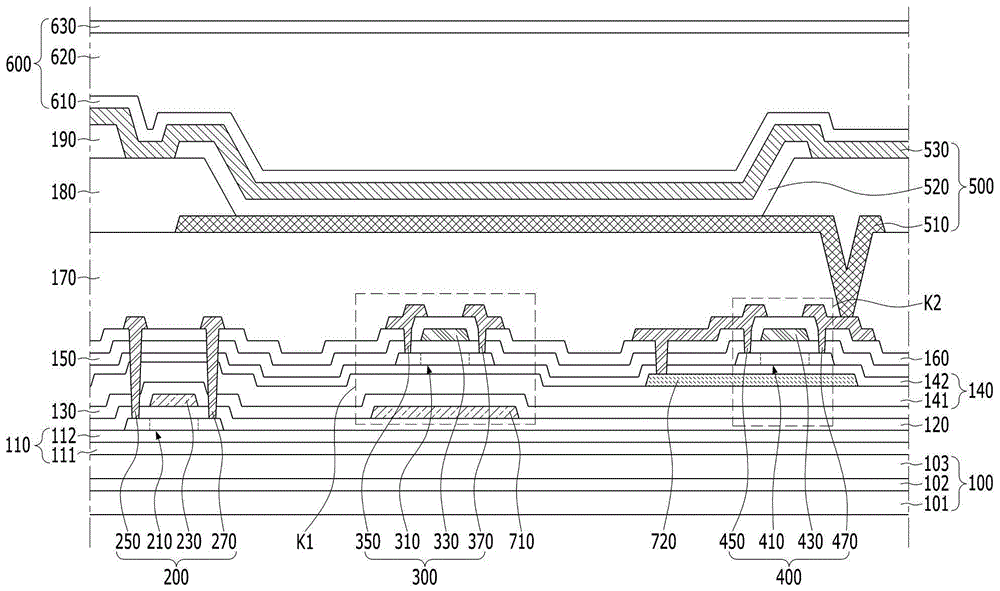
图1是示意性地示出根据本公开的示例性实施例的显示装置的视图。图2是沿着图1的线I-I'截取的横截面的示例。图3A是图2中的K1区域的放大图的示例。图3B是图2中的K2区域的放大图的示例。FIG. 1 is a view schematically illustrating a display device according to an exemplary embodiment of the present disclosure. FIG. 2 is an example of a cross section taken along line II' of FIG. 1 . FIG. 3A is an example of an enlarged view of the K1 region in FIG. 2 . FIG. 3B is an example of an enlarged view of the K2 region in FIG. 2 .
参考图1、图2、图3A和图3B,根据本公开的示例性实施例的显示装置可以包括显示面板DP和驱动部件。显示面板DP可以实现向用户提供的图像。例如,显示面板DP可以包括多个像素区域PA。驱动部件可以向显示面板DP的每个像素区域PA提供用于实现图像的各种信号。例如,驱动部件可以包括扫描驱动器SD、数据驱动器DD和时序控制器TC。Referring to FIGS. 1 , 2 , 3A, and 3B, a display device according to an exemplary embodiment of the present disclosure may include a display panel DP and a driving part. The display panel DP can realize images provided to the user. For example, the display panel DP may include a plurality of pixel areas PA. The driving part may supply various signals for realizing an image to each pixel area PA of the display panel DP. For example, the driving part may include a scan driver SD, a data driver DD, and a timing controller TC.
扫描驱动器SD可以通过扫描线将扫描信号依次施加到显示面板DP的每个像素区域PA。数据驱动器DD可以通过数据线将数据信号施加到显示面板DP的每个像素区域PA。时序控制器TC可以控制扫描驱动器SD的操作和数据驱动器DD的操作。例如,时序控制器TC可以将时钟信号、复位时钟信号和启动信号供应给扫描驱动器SD,并且将数字视频数据和源极时序控制信号供应给数据驱动器DD。The scan driver SD may sequentially apply scan signals to each pixel area PA of the display panel DP through scan lines. The data driver DD may apply a data signal to each pixel area PA of the display panel DP through a data line. The timing controller TC may control the operation of the scan driver SD and the operation of the data driver DD. For example, the timing controller TC may supply a clock signal, a reset clock signal, and a start signal to the scan driver SD, and supply digital video data and a source timing control signal to the data driver DD.
显示面板DP中的像素区域PA中的每一个可以实现(或产生)特定颜色。例如,发光器件500可以设置在每个像素区域PA中。发光器件500可以发射具有特定颜色的光。例如,发光器件500可以包括依次堆叠的第一电极510、发光层520和第二电极530。Each of the pixel areas PA in the display panel DP may implement (or generate) a specific color. For example, the
第一电极510可以包括导电材料。第一电极510可以包括具有高反射率的材料。例如,第一电极510可以包括诸如铝(Al)和/或银(Ag)的金属。第一电极510可以具有多层结构。例如,第一电极510可以具有以下结构:其中由金属制成的反射电极插设在由诸如氧化铟锡(ITO)和/或氧化铟锌(IZO)的透明导电材料制成的透明电极之间。The
发光层520可以生成具有与第一电极510和第二电极530之间的电压差相对应的亮度的光。例如,发光层520可以包括具有发射材料的发射材料层(EML)。发射材料可以包括有机材料、无机材料或混合材料。例如,根据本公开的示例性实施例的显示装置的显示面板DP可以是包括有机发射材料的有机发光显示面板。发光层520可以具有多层结构。例如,发光层520还可以包括空穴注入层(HIL)、空穴传输层(HTL)、电子传输层(ETL)和电子注入层(EIL)中的至少一个。因此,在根据本公开的示例性实施例的显示装置的显示面板DP中,可以提高每个像素区域PA中的发光层520的发光效率。The
第二电极530可以包括导电材料。第二电极530可以包括与第一电极510不同的材料。第二电极530的透射率可以高于第一电极510的透射率。例如,第二电极530可以包括诸如ITO和/或IZO的透明导电材料。因此,在根据本公开的示例性实施例的显示装置的显示面板DP中,每个像素区域PA的发光层520生成的光可以通过对应的像素区域PA的第二电极530被发射到外部。The
每个像素区域PA的发光器件500可以由器件基板100支撑。器件基板100可以具有多层结构。例如,器件基板100可以具有第一基板层101、基板绝缘层102和第二基板层103的堆叠结构。第二基板层103可以包括与第一基板层101相同的材料。例如,第一基板层101和第二基板层103可以包括诸如聚酰亚胺(PI)的聚合物材料。基板绝缘层102可以包括绝缘材料。例如,基板绝缘层102可以包括诸如氧化硅(SiO)和/或氮化硅(SiN)的无机绝缘材料。因此,在根据本公开的示例性实施例的显示装置的显示面板DP中,可以防止由于外部冲击和弯曲而对器件基板100和/或发光器件500造成损坏。The
驱动电路可以设置在器件基板100的每个像素区域PA中。每个像素区域PA的驱动电路可以被电连接至诸如扫描驱动器SD、数据驱动器DD和时序控制器TC的驱动部件。例如,每个像素区域PA的驱动电路可以被电连接至扫描线中的一个和数据线中的一个。每个像素区域PA的驱动电路可以根据扫描信号生成对应于数据信号的驱动电流。例如,每个像素区域PA的驱动电路可以包括第一开关薄膜晶体管200、第二开关薄膜晶体管300和驱动薄膜晶体管400。A driving circuit may be disposed in each pixel area PA of the
第一开关薄膜晶体管200可以包括设置在器件基板100上的第一半导体图案210、第一栅电极230、第一源电极250和第一漏电极270。The first switching
第一半导体图案210可以靠近器件基板100设置。第一半导体图案210可以包括半导体材料。例如,第一半导体图案210可以包括低温多晶硅(LTPS)。第一半导体图案210可以包括第一源极区、第一沟道区和第一漏极区。第一沟道区可以设置在第一源极区与第一漏极区之间。第一源极区和第一漏极区可以具有低于第一沟道区的电阻。例如,第一源极区和第一漏极区可以包括导电杂质。The
第一栅电极230可以设置在第一半导体图案210上。第一栅电极230可以包括导电材料。例如,第一栅电极230可以包括诸如铝(Al)、钛(Ti)、铜(Cu)、铬(Cr)、钼(Mo)和/或钨(W)的金属。第一栅电极230可以与第一半导体图案210绝缘。例如,在第一半导体图案210与第一栅电极230之间延伸的第一栅极绝缘层120可以设置在器件基板100上。第一栅极绝缘层120可以包括绝缘材料。例如,第一栅极绝缘层120可以包括诸如氧化硅(SiO)和/或氮化硅(SiN)的无机绝缘材料。第一栅极绝缘层120可以延伸超出第一半导体图案210。例如,第一半导体图案210的侧面可以被第一栅极绝缘层120覆盖。The
第一栅电极230可以与第一半导体图案210的第一沟道区重叠(叠置)。例如,第一半导体图案210的第一沟道区可以具有与施加到第一栅电极230的电压对应的电导率。The
第一源电极250可以包括导电材料。例如,第一源电极250可以包括诸如铝(Al)、钛(Ti)、铜(Cu)、铬(Cr)、钼(Mo)和/或钨(W)的金属。第一源电极250可以与第一栅电极230绝缘。第一源电极250可以包括与第一栅电极230不同的材料。第一源电极250可以设置在与第一栅电极230不同的层上。例如,在第一栅电极230与第一源电极250之间延伸的第一层间绝缘层130可以设置在第一栅极绝缘层120上。第一层间绝缘层130可以包括绝缘材料。例如,第一层间绝缘层130可以包括由氮化硅(SiN)制成的无机绝缘材料。第一层间绝缘层130可以延伸超出第一半导体图案210和第一栅电极230。例如,第一栅电极230的侧面可以被第一层间绝缘层130覆盖。The
第一源电极250可以被电连接至第一半导体图案210的第一源极区。例如,第一栅极绝缘层120和第一层间绝缘层130可以包括部分地暴露第一半导体图案210的第一源极区的第一源极接触孔。第一源电极250可以通过第一源极接触孔与第一半导体图案210的第一源极区直接接触。The
第一漏电极270可以包括导电材料。例如,第一漏电极270可以包括诸如铝(Al)、钛(Ti)、铜(Cu)、铬(Cr)、钼(Mo)和/或钨(W)的金属。第一漏电极270可以与第一栅电极230绝缘。第一漏电极270可以包括与第一栅电极230不同的材料。第一漏电极270可以设置在与第一栅电极230不同的层上。例如,第一层间绝缘层130可以在第一栅电极230与第一漏电极270之间延伸。第一漏电极270可以设置在与第一源电极250相同的层上(即,第一漏电极270和第一源电极250可以设置在同一层上)。例如,第一漏电极270可以包括与第一源电极250相同的材料。The
第一漏电极270可以被电连接至第一半导体图案210的第一漏极区。例如,第一栅极绝缘层120和第一层间绝缘层130可以包括部分地暴露第一半导体图案210的第一漏极区的第一漏极接触孔。第一漏电极270可以通过第一漏极接触孔与第一半导体图案210的第一漏极区直接接触。The
第二开关薄膜晶体管300可以与第一开关薄膜晶体管200间隔开(或分开)。第二开关薄膜晶体管300的结构可以与第一开关薄膜晶体管200的结构相同。例如,第二开关薄膜晶体管300可以包括设置在器件基板100上的第二半导体图案310、第二栅电极330、第二源电极350和第二漏电极370。The second switching
第二半导体图案310可以包括半导体材料。第二半导体图案310可以包括与第一半导体图案210不同的材料。例如,第二半导体图案310可以包括诸如氧化铟镓锌(IGZO)的氧化物半导体。第二半导体图案310可以包括第二源极区、第二沟道区和第二漏极区。第二沟道区可以设置在第二源极区与第二漏极区之间。第二源极区和第二漏极区可以具有低于第二沟道区的电阻。例如,第二源极区和第二漏极区可以包括氧化物半导体的导体化区。The
第二半导体图案310可以设置在与第一半导体图案210不同的层上。例如,隔离绝缘层140可以设置在第一层间绝缘层130上,并且第二半导体图案310可以设置在隔离绝缘层140上。隔离绝缘层140可以包括绝缘材料。隔离绝缘层140可以具有多层结构。例如,隔离绝缘层140可以具有第一隔离绝缘层141和第二隔离绝缘层142的堆叠结构。第二隔离绝缘层142可以包括与第一隔离绝缘层141相同的材料。例如,第一隔离绝缘层141和第二隔离绝缘层142可以包括由氧化硅(SiO)制成的无机绝缘材料。因此,在根据本公开的示例性实施例的显示装置的显示面板DP中,可以防止由于形成第二半导体图案310的工艺而对第一半导体图案210造成损坏。此外,在根据本公开的示例性实施例的显示装置的显示面板DP中,可以防止由于从隔离绝缘层140发出的氢而导致每个像素区域PA中的第二半导体图案310的非预期导体化。在一个或多个方面,术语“导体化”可以指使得层(例如,半导体层)的至少一部分导电。The
第二栅电极330可以设置在第二半导体图案310上。第二栅电极330可以包括导电材料。例如,第二栅电极330可以包括诸如铝(Al)、钛(Ti)、铜(Cu)、铬(Cr)、钼(Mo)和/或钨(W)的金属。第二栅电极330可以与第二半导体图案310绝缘。例如,在第二半导体图案310与第二栅电极330之间延伸的第二栅极绝缘层150可以设置在隔离绝缘层140上。第二栅极绝缘层150可以包括绝缘材料。例如,第二栅极绝缘层150可以是由诸如氧化硅(SiO)的无机绝缘材料制成的无机绝缘层。第二栅极绝缘层150可以延伸超出第二半导体图案310。例如,第二半导体图案310的侧面可以被第二栅极绝缘层150覆盖。The
第二栅电极330可以与第二半导体图案310的第二沟道区重叠。例如,第二半导体图案310的第二沟道区可以具有与施加到第二栅电极330的电压对应的电导率。The
第二源电极350可以包括导电材料。例如,第二源电极350可以包括诸如铝(Al)、钛(Ti)、铜(Cu)、铬(Cr)、钼(Mo)和/或钨(W)的金属。第二源电极350可以与第二栅电极330绝缘。第二源电极350可以包括与第二栅电极330不同的材料。第二源电极350可以设置在与第二栅电极330不同的层上。例如,在第二栅电极330与第二源电极350之间延伸的第二层间绝缘层160可以设置在器件基板100上。第二层间绝缘层160可以包括绝缘材料。例如,第二层间绝缘层160可以是由诸如氮化硅(SiN)和/或氧化硅(SiO)的无机绝缘材料制成的无机绝缘层。第二层间绝缘层160可以延伸超出第二半导体图案310和第二栅电极330。例如,第二栅电极330的侧面可以被第二层间绝缘层160覆盖。The
第二源电极350可以包括与第一源电极250和第一漏电极270相同的材料。第一源电极250和第一漏电极270可以设置在与第二源电极350相同的层上。例如,第一源电极250和第一漏电极270可以设置在第二层间绝缘层160上。第一源极接触孔和第一漏极接触孔可以穿透隔离绝缘层140、第二栅极绝缘层150和第二层间绝缘层160。The
第二源电极350可以被电连接至第二半导体图案310的第二源极区。例如,第二栅极绝缘层150和第二层间绝缘层160可以包括部分地暴露第二半导体图案310的第二源极区的第二源极接触孔。第二源电极350可以通过第二源极接触孔与第二半导体图案310的第二源极区直接接触。The
第二漏电极370可以包括导电材料。例如,第二漏电极370可以包括诸如铝(Al)、钛(Ti)、铜(Cu)、铬(Cr)、钼(Mo)和/或钨(W)的金属。第二漏电极370可以与第二栅电极330绝缘。第二漏电极370可以包括与第二栅电极330不同的材料。第二漏电极370可以设置在与第二栅电极330不同的层上。例如,第二漏电极370可以设置在第二层间绝缘层160上。第二漏电极370可以设置在与第二源电极350相同的层上。例如,第二漏电极370可以包括与第二源电极350相同的材料。The
第二漏电极370可以被电连接至第二半导体图案310的第二漏极区。例如,第二栅极绝缘层150和第二层间绝缘层160可以包括部分地暴露第二半导体图案310的第二漏极区的第二漏极接触孔。第二漏电极370可以通过第二漏极接触孔与第二半导体图案310的第二漏极区直接接触。The
驱动薄膜晶体管400可以与第一开关薄膜晶体管200和第二开关薄膜晶体管300间隔开(或分开)。驱动薄膜晶体管400可以具有与第二开关薄膜晶体管300相同的结构。例如,驱动薄膜晶体管400可以包括设置在隔离绝缘层140上的驱动半导体图案410、驱动栅电极430、驱动源电极450和驱动漏电极470。The driving
驱动半导体图案410可以包括半导体材料。例如,驱动半导体图案410可以包括诸如IGZO的氧化物半导体。驱动半导体图案410可以包括与第二半导体图案310相同的材料。例如,驱动半导体图案410可以设置在与第二半导体图案310相同的层上。驱动半导体图案410可以与第二半导体图案310同时形成。驱动半导体图案410可以包括第三源极区、第三沟道区和第三漏极区。第三沟道区可以设置在第三源极区与第三漏极区之间。第三源极区和第三漏极区可以具有低于第三沟道区的电阻。例如,第三源极区和第三漏极区可以包括氧化物半导体的导体化区。驱动半导体图案410的第三沟道区可以具有与第二半导体图案310的第二沟道区相同的电阻。例如,驱动半导体图案410的第三源极区和第三漏极区可以具有与第二半导体图案310的第二源极区和第二漏极区相同的电阻。The driving
驱动栅电极430可以设置在驱动半导体图案410上。驱动栅电极430可以包括导电材料。例如,驱动栅电极430可以包括诸如铝(Al)、钛(Ti)、铜(Cu)、铬(Cr)、钼(Mo)和/或钨(W)的金属。驱动栅电极430可以与驱动半导体图案410绝缘。例如,第二栅极绝缘层150可以在驱动半导体图案410与驱动栅电极430之间延伸。驱动半导体图案410的侧面可以被第二栅极绝缘层150覆盖。驱动栅电极430可以包括与第二开关薄膜晶体管300的第二栅电极330相同的材料。The driving
驱动栅电极430可以与驱动半导体图案410的第三沟道区重叠。例如,驱动半导体图案410的第三沟道区可以具有与施加到驱动栅电极430的电压对应的电导率。The driving
驱动源电极450可以包括导电材料。例如,驱动源电极450可以包括诸如铝(Al)、钛(Ti)、铜(Cu)、铬(Cr)、钼(Mo)和/或钨(W)的金属。驱动源电极450可以与驱动栅电极430绝缘。驱动源电极450可以包括与驱动栅电极430不同的材料。驱动源电极450可以设置在与驱动栅电极430不同的层上。例如,第二层间绝缘层160可以在驱动栅电极430与驱动源电极450之间延伸。驱动源电极450可以包括第二源电极350和第二漏电极370。例如,驱动源电极450可以设置在与第二源电极350和第二漏电极370相同的层上。The driving
驱动源电极450可以被电连接至驱动半导体图案410的第三源极区。例如,第二栅极绝缘层150和第二层间绝缘层160可以包括部分地暴露驱动半导体图案410的第三源极区的第三源极接触孔。驱动源电极450可以通过第三源极接触孔与驱动半导体图案410的第三源极区直接接触。The driving
驱动漏电极470可以包括导电材料。例如,驱动漏电极470可以包括诸如铝(Al)、钛(Ti)、铜(Cu)、铬(Cr)、钼(Mo)和/或钨(W)的金属。驱动漏电极470可以与驱动栅电极430绝缘。驱动漏电极470可以包括与驱动栅电极430不同的材料。驱动漏电极470可以设置在与驱动栅电极430不同的层上。例如,第二层间绝缘层160可以在驱动栅电极430与驱动漏电极470之间延伸。驱动漏电极470可以设置在与驱动源电极450相同的层上。例如,驱动漏电极470可以包括与驱动源电极450相同的材料。The driving
驱动漏电极470可以被电连接至驱动半导体图案410的第三漏极区。例如,第二栅极绝缘层150和第二层间绝缘层160可以包括部分地暴露驱动半导体图案410的驱动漏极区的第三漏极接触孔。驱动漏电极470可以通过第三漏极接触孔与驱动半导体图案410的第三漏极区直接接触。The driving
在所述驱动电路中的每一个中,第一开关薄膜晶体管200和/或第二开关薄膜晶体管300可以根据扫描信号将数据信号传输到驱动薄膜晶体管400。例如,在每个像素区域PA中,第一开关薄膜晶体管200的第一栅电极230可以被电连接至扫描线中的一个,第一开关薄膜晶体管200的第一源电极250可以被电连接至数据线中的一个。在每个驱动电路中,未连接至数据线中的一个的第二开关薄膜晶体管300可以用作内部补偿电路,以根据像素区域PA的位置来补偿信号延迟。例如,在每个像素区域PA中,第二开关薄膜晶体管300的第二源电极350可以被电连接至参考电压供应线中的一个。每个驱动电路的驱动薄膜晶体管400可以生成对应于数据信号的驱动电流。例如,在每个像素区域PA中,驱动薄膜晶体管400的驱动栅电极430可以被电连接至第一开关薄膜晶体管200的第一漏电极270,驱动薄膜晶体管400的驱动源电极450可以被电连接至电源电压供应线中的一个。In each of the driving circuits, the first switching
扫描线、数据线、参考电压供应线和电源电压供应线可以通过在每个像素区域PA中形成第一开关薄膜晶体管200、第二开关薄膜晶体管300和驱动薄膜晶体管400的工艺形成。例如,扫描线可以与每个驱动电路的第一栅电极230设置在同一层上,数据线、参考电压供应线和电源电压供应线可以与每个驱动电路的第一栅电极250和第一漏电极270设置在同一层上。扫描线可以包括与每个驱动电路的第一栅电极230相同的材料。例如,扫描线可以设置在第一栅极绝缘层120与第一层间绝缘层130之间。数据线、参考电压供应线和电源电压供应线可以包括与每个驱动电路的第一源电极250、第一漏电极270、第二源电极350、第二漏电极370、驱动源电极450和驱动漏电极470相同的材料。例如,数据线、参考电压供应线和电源电压供应线可以设置在第二层间绝缘层160上。The scan line, the data line, the reference voltage supply line and the power supply voltage supply line may be formed through a process of forming the first switching
缓冲绝缘层110可以设置在器件基板100与每个驱动电路之间。缓冲绝缘层110可以防止在形成每个驱动电路的过程中由于器件基板100造成污染。例如,器件基板100的朝向每个驱动电路的第一开关薄膜晶体管200、第二开关薄膜晶体管300和驱动薄膜晶体管400的上表面可以被缓冲绝缘层110完全覆盖。缓冲绝缘层110可以包括绝缘材料。例如,缓冲绝缘层110可以包括诸如氧化硅(SiO)和/或氮化硅(SiN)的无机绝缘材料。缓冲绝缘层110可以具有多层结构。例如,缓冲绝缘层110可以具有第一缓冲层111和第二缓冲层112的堆叠结构。第二缓冲层112可以包括与第一缓冲层111不同的材料。例如,缓冲绝缘层110可以具有由氧化硅(SiO)制成的无机绝缘层和由氮化硅(SiN)制成的无机绝缘层的堆叠结构。A
每个像素区域PA的发光器件500可以被电连接至对应像素区域PA中的驱动电路的驱动薄膜晶体管400。例如,每个像素区域PA中的发光器件500的第一电极510可以被电连接至对应像素区域PA中的驱动薄膜晶体管400的驱动漏电极470。每个像素区域PA的第一电极510可以设置在与对应像素区域PA的驱动漏电极470不同的层上。例如,覆盖第一源电极250、第一漏电极270、第二源电极350、第二漏电极370、驱动源电极450和驱动漏电极470的外涂层170可以设置在第二层间绝缘层160上,每个像素区域PA的发光器件500可以设置在外涂层170上。外涂层170可以包括绝缘材料。外涂层170可以包括与第二层间绝缘层160不同的材料。例如,外涂层170可以是由有机绝缘材料制成的有机绝缘层。由于每个像素区域PA的驱动电路引起的厚度差异可以通过外涂层170消除。例如,外涂层170可以用于消除由于每个像素区域PA的第一开关薄膜晶体管200、第二开关薄膜晶体管300和驱动薄膜晶体管400引起的厚度差异。与器件基板100相反(对置)的外涂层170的上表面可以是平坦表面。The
每个像素区域PA的第一电极510可以通过穿透外涂层170被电连接至对应像素区域PA的驱动漏电极470。例如,外涂层170可以包括部分地暴露每个像素区域PA的驱动漏电极470的多个电极接触孔。每个像素区域PA的第一电极510可以通过所述多个电极接触孔中的一个与对应像素区域PA的驱动漏电极470直接接触。The
每个像素区域PA的发光器件500可以发射具有与相邻像素区域PA的发光器件500不同的亮度的光。例如,每个像素区域PA中的发光器件500的第一电极510可以与相邻像素区域PA中的发光器件500的第一电极510间隔开(或分开)。堤部绝缘层180可以设置在相邻的两个像素区域PA的第一电极510之间的外涂层170上。堤部绝缘层180可以包括绝缘材料。例如,堤部绝缘层180可以是由有机绝缘材料制成的有机绝缘层。堤部绝缘层180可以包括与外涂层170不同的材料。每个像素区域PA中的发光器件500的第一电极510可以通过堤部绝缘层180与相邻像素区域PA中的发光器件500的第一电极510绝缘。例如,堤部绝缘层180可以覆盖每个像素区域PA中的第一电极510的边缘。每个像素区域PA中的发光层520和第二电极530可以依次堆叠在对应第一电极510的被堤部绝缘层180暴露的部分上。The
从每个像素区域PA的发光器件500发射的光可以显示不同于从相邻像素区域PA的发光器件500发射的光的颜色。例如,每个像素区域PA的发光层520可以与相邻像素区域PA的发光层520间隔开(或分开)。每个像素区域PA中的发光层520可以包括设置在堤部绝缘层180上的端部。每个像素区域PA的发光层520可以单独形成。例如,每个像素区域PA的发光层520可以使用精细金属掩模(FMM)形成。间隔件190可以设置在堤部绝缘层180上。间隔件190可以防止由于精细金属掩模而对堤部绝缘层180和发光层520造成损坏。间隔件190可以包括绝缘材料。例如,间隔件190可以是由有机绝缘材料制成的有机绝缘层。每个像素区域PA中的发光层520的端部可以与间隔件190间隔开(或分开)。Light emitted from the
施加到每个像素区域PA的第二电极530的电压可以与施加到相邻像素区域PA的第二电极530的电压相同。例如,每个像素区域PA的第二电极530可以被电连接至相邻像素区域PA的第二电极530。每个像素区域PA的第二电极530可以包括与相邻像素区域PA的第二电极530相同的材料。例如,每个像素区域PA的第二电极530可以与相邻像素区域PA的第二电极530直接接触。每个像素区域PA的第二电极530可以延伸到堤部绝缘层180和间隔件190上。因此,在根据本公开的示例性实施例的显示装置的显示面板DP中,从每个像素区域PA的发光器件500发射的光的亮度可以由对应像素区域PA的驱动电路生成的驱动电流控制。The voltage applied to the
封装元件600可以设置在每个像素区域PA的发光器件500上。封装元件600可以防止由于外部冲击和湿气(水分)对每个像素区域PA中的发光器件500造成损坏。封装元件600可以包括绝缘材料。封装元件600可以具有多层结构。例如,封装元件600可以包括依次堆叠的第一封装层610、第二封装层620和第三封装层630。第二封装层620可以包括与第一封装层610和第三封装层630不同的材料。例如,第一封装层610和第三封装层630可以是由无机绝缘材料制成的无机绝缘层,第二封装层620可以是由有机绝缘材料制成的有机绝缘层。因此,在根据本公开的示例性实施例的显示装置的显示面板DP中,可以有效地防止由于外部冲击和湿气对每个像素区域PA中的发光器件500造成损坏。每个像素区域PA的发光器件500中的厚度差异可以通过第二封装层620消除。例如,封装元件600的与器件基板100相反的上表面可以是平坦表面。A
根据本公开的示例性实施例的显示装置的显示面板DP可以防止包括氧化物半导体的半导体图案(例如,第二半导体图案310和驱动半导体图案410)的特性由于外部光而发生变化。例如,遮光图案可以设置在每个像素区域PA中。遮光图案可以遮挡(阻挡)在朝向包括氧化物半导体的半导体图案的方向上行进的外部光。例如,每个像素区域PA的遮光图案可以包括在器件基板100与第二半导体图案310之间的第一遮光图案710以及在器件基板100与驱动半导体图案410之间的第二遮光图案720。The display panel DP of a display device according to an exemplary embodiment of the present disclosure may prevent characteristics of semiconductor patterns including oxide semiconductors (for example, the
第一遮光图案710可以遮挡穿过器件基板100在朝向第二半导体图案310的方向上行进的外部光。第一遮光图案710可以具有大于第二半导体图案310的尺寸。例如,第二半导体图案310可以与第一遮光图案710的一部分重叠。第一遮光图案710可以与第一开关薄膜晶体管200和驱动薄膜晶体管400间隔开(或分开)。例如,第一遮光图案710可以设置在第一开关薄膜晶体管200和驱动薄膜晶体管400的外部。The first
第一遮光图案710可以包括导电材料。例如,第一遮光图案710可以包括诸如铝(Al)、钛(Ti)、铜(Cu)、铬(Cr)、钼(Mo)和/或钨(W)的金属。第一遮光图案710可以通过形成第一开关薄膜晶体管200的工艺形成。例如,第一遮光图案710可以与第一栅电极230同时形成。第一遮光图案710可以包括与第一栅电极230相同的材料。第一遮光图案710可以设置在与第一栅电极230相同的层上。例如,第一遮光图案710可以设置在第一栅极绝缘层120与第一层间绝缘层130之间。The first light-
第二遮光图案720可以遮挡穿过器件基板100在朝向驱动半导体图案410的方向上行进的外部光。第二遮光图案720可以具有大于驱动半导体图案410的尺寸。例如,驱动半导体图案410可以与第二遮光图案720的一部分重叠。第二遮光图案720可以与第一开关薄膜晶体管200和第二开关薄膜晶体管200间隔开(或分开)。例如,第二遮光图案720可以设置在第一开关薄膜晶体管200和第二开关薄膜晶体管300的外部。The second
第二遮光图案720可以包括导电材料。例如,第二遮光图案720可以包括金属。第二遮光图案720可以包括与第一遮光图案710不同的材料。例如,第二遮光图案720可以包括能够阻止氢的渗透的材料。第二遮光图案720可以包括与氢稳定耦合的材料。例如,第二遮光图案720可以包括钛(Ti)。因此,在根据本公开的示例性实施例的显示装置的显示面板DP中,由于形成第一半导体图案210的工艺而残留在器件基板100与隔离绝缘层140之间的氢通过第二遮光图案720(的阻挡)而不能渗透到驱动半导体图案中。也就是说,在根据本公开的示例性实施例的显示装置的显示面板DP中,可以通过第二遮光图案720防止每个像素区域PA中的驱动半导体图案410的非预期导体化。因此,在根据本公开的示例性实施例的显示装置的显示面板DP中,每个像素区域PA中的驱动薄膜晶体管400的操作特性的可靠性可以得到改善。The second
第二遮光图案720可以设置在与第一遮光图案710不同的层上。第二遮光图案720可以靠近驱动半导体图案410设置。例如,第二遮光图案720可以设置在第一隔离绝缘层141与第二隔离绝缘层142之间。第二遮光图案720与驱动半导体图案410之间的距离d2可以小于第一遮光图案710与第二半导体图案310之间的距离d1。The second light-
可以将特定电压施加到第二遮光图案720。施加到第二遮光图案720的电压可以不同于施加到驱动栅电极430的电压。例如,第二遮光图案720可以被电连接至驱动源电极450。可以将恒定电压施加到第二遮光图案720,而不管施加到驱动栅电极430的电压如何。因此,在根据本发明的实施例的显示装置的显示面板DP中,具有第一电容C1的寄生电容器可以形成在每个像素区域PA中的第二遮光图案720和驱动半导体图案410之间。可以在每个像素区域PA中的驱动半导体图案410和驱动栅电极430之间形成具有第二电容C2的寄生电容器。在根据本公开的示例性实施例的显示装置的显示面板DP中,影响施加到像素区域PA中的发光器件500的驱动电流的有效栅极电压的变化量可以由以下等式(方程)确定。在本文中,ΔVeff表示有效栅极电压的变化量,ΔVGAT表示施加到驱动栅电极430的电压的变化量,CACT表示由施加到驱动半导体图案410的第三源极区和第三漏极区的电压形成的寄生电容器的电容。A specific voltage may be applied to the second light-
[等式][equation]
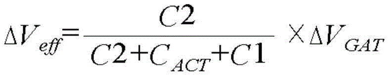
参考所述等式,在根据本公开的示例性实施例的显示装置的显示面板DP中,影响驱动电流的生成的有效栅极电压可以通过在每个像素区域PA中的第二遮光图案720和驱动半导体图案410之间形成的寄生电容器而降低。在典型的薄膜晶体管中,当有效栅极电压降低时,S因子可能增加并且根据施加电压的电流的变化率可能降低。在本文中,S因子是指根据薄膜晶体管的ON-OFF(导通-截止)过渡区中的栅极电压变化的电流变化量的反比。此外,当显示面板DP的每个像素区域PA中的驱动薄膜晶体管400的S因子增加并且根据施加到驱动栅电极430的电压的电流的变化率减小时,低灰度斑点的出现(发生)率可能降低。因此,根据本公开的示例性实施例的显示装置的显示面板DP可以通过在对应像素区域PA中的第二遮光图案720和驱动半导体图案410之间形成寄生电容器来增加每个像素区域PA中的驱动薄膜晶体管400的S因子,并且可以减小根据施加到驱动薄膜晶体管400的驱动栅电极430的电压的驱动电流的变化率。也就是说,在根据本公开的示例性实施例的显示装置的显示面板DP中,可以控制每个像素区域PA中的驱动薄膜晶体管400的特性,而无需改变对应像素区域PA中的第一开关薄膜晶体管200和第二开关薄膜晶体管300的结构。因此,在根据本公开的示例性实施例的显示装置的显示面板DP中,可以防止低灰度斑点的出现,而无需改变每个像素区域PA中的第一开关薄膜晶体管200和第二开关薄膜晶体管300的特性。Referring to the equation, in the display panel DP of the display device according to an exemplary embodiment of the present disclosure, an effective gate voltage affecting generation of a driving current may pass through the second light-
图4是示出根据对应像素区域中的第一电容与第二电容之比的每个像素区域中的驱动薄膜晶体管的S因子的视图的示例。FIG. 4 is an example of a view illustrating an S factor of a driving thin film transistor in each pixel area according to a ratio of a first capacitance to a second capacitance in a corresponding pixel area.
参考图4,每个像素区域PA中的驱动薄膜晶体管400的S因子可以与对应像素区域PA中的第一电容C1与第二电容C2之比成比例。因此,根据本公开的示例性实施例的显示装置的显示面板DP可以通过增加在每个像素区域PA中的第二遮光图案720和驱动半导体图案410之间形成的寄生电容器的第一电容C1来有效地增加每个像素区域PA中的驱动薄膜晶体管400的S因子。例如,在根据本公开的示例性实施例的显示装置的显示面板DP中,在每个像素区域PA中,第二隔离绝缘层142可以具有比第一隔离绝缘层141薄的厚度。也就是说,在根据本公开的示例性实施例的显示装置的显示面板DP中,在每个像素区域PA中,第二遮光图案720可以设置成靠近驱动半导体图案410。例如,第二隔离绝缘层142可以具有比第二栅极绝缘层150薄的厚度。因此,在根据本公开的示例性实施例的显示装置的显示面板DP中,可以有效地防止出现低灰度斑点。Referring to FIG. 4 , the S factor of the driving
因此,根据本公开的示例性实施例的显示装置可以包括:第一开关薄膜晶体管200,其包括由硅制成的第一半导体图案210;第二开关薄膜晶体管300,其包括由氧化物半导体制成的第二半导体图案310;驱动薄膜晶体管400,其包括由氧化物半导体制成的驱动半导体图案410;在显示面板DP的每个像素区域PA中与第二半导体图案310重叠的第一遮光图案710以及与驱动半导体图案410重叠的第二遮光图案720,其中,第二遮光图案720与驱动半导体图案410之间的距离d2可以小于第一遮光图案710与第二半导体图案310之间的距离d1。因此,在根据本公开的示例性实施例的显示装置的显示面板DP中,可以增加每个像素区域PA中的驱动薄膜晶体管400的S因子,而无需改变每个像素区域PA中的第一开关薄膜晶体管200和第二开关薄膜晶体管300的结构。因此,在根据本公开的示例性实施例的显示装置的显示面板DP中,可以有效地防止出现低灰度斑点。Therefore, a display device according to an exemplary embodiment of the present disclosure may include: a first switching
此外,在根据本公开的示例性实施例的显示装置的显示面板DP中,第二遮光图案720的尺寸可以大于驱动半导体图案410的尺寸。因此,在根据本公开的示例性实施例的显示装置的显示面板DP中,从靠近驱动半导体图案410设置的第二遮光图案720的端部衍射的光可以不照射到驱动半导体图案410。因此,在根据本公开的示例性实施例的显示装置的显示面板DP中,可以有效地防止驱动半导体图案410的特性由于外部光而改变。Also, in the display panel DP of the display device according to an exemplary embodiment of the present disclosure, the size of the second
在根据本公开的另一示例性实施例的显示装置中,可以将特定电压施加到第一遮光图案710。施加到第一遮光图案710的电压可以与施加到第二栅电极330的电压相同。例如,第一遮光图案710可以被电连接至第二栅电极330。因此,在根据本公开的另一示例性实施例的显示装置的显示面板DP中,每个像素区域PA中的第一遮光图案710可以用作对应像素区域PA中的第二开关薄膜晶体管300的双栅电极中的一个栅电极。也就是说,在根据本公开的另一示例性实施例的显示装置的显示面板DP中,每个像素区域PA中的第二半导体图案310的第二沟道区可以具有与施加到对应像素区域PA中的第二栅电极330的电压和施加到对应像素区域PA中的第一遮光图案710的电压相对应的电导率。因此,在根据本公开的另一示例性实施例的显示装置的显示面板DP中,可以改善每个像素区域PA中的第二开关薄膜晶体管300的操作特性。例如,在根据本公开的另一示例性实施例的显示装置的显示面板DP中,每个像素区域PA中的第二开关薄膜晶体管300可以被快速地导通。In a display device according to another exemplary embodiment of the present disclosure, a specific voltage may be applied to the first light-
根据本公开的示例性实施例的显示装置提出,第一遮光图案710与第一栅电极230同时形成。然而,在根据本公开的另一示例性实施例的显示装置中,第一遮光图案710可以通过与形成第一栅电极230的工艺不同的工艺形成。例如,在根据本公开的另一示例性实施例的显示装置中,第一遮光图案710可以包括能够阻止氢的渗透的材料。因此,在根据本公开的另一示例性实施例的显示装置中,可以防止每个像素区域PA中的第二半导体图案310由于残留的氢而导致非预期导体化。也就是说,在根据本公开的另一示例性实施例的显示装置中,可以防止每个像素区域PA中的第二开关薄膜晶体管300出现故障。因此,在根据本公开的另一示例性实施例的显示装置中,可以有效地防止出现低灰度斑点。第一遮光图案710可以包括与第二遮光图案720相同的材料。例如,第一遮光图案可以包括钛(Ti)。The display device according to an exemplary embodiment of the present disclosure proposes that the first light-
根据本公开的另一示例性实施例的显示装置还可以包括位于每个像素区域中的隔离绝缘层和外涂层之间的存储电容器。该存储电容器可以具有电容器下电极和电容器上电极的堆叠结构。在根据本公开的另一示例性实施例的显示装置中,存储电容器800可以包括设置在与第二遮光图案720相同的层上的电容器下电极810和设置在与驱动栅电极430相同的层上的电容器上电极820,如图5所示。因此,在根据本公开的另一示例性实施例的显示装置中,存储电容器800的电容器下电极810和电容器上电极820可以设置在与诸如扫描线、数据线、参考电压供应线和/或电源电压供应线的信号线不同的层上。也就是说,在根据本公开的另一示例性实施例的显示装置中,可以防止由于施加到信号线的信号而导致存储在每个驱动电路的存储电容器800中的电压出现偏差。因此,在根据本公开的另一示例性实施例的显示装置中,驱动电路中的每一个可以稳定地操作。A display device according to another exemplary embodiment of the present disclosure may further include a storage capacitor between the isolation insulating layer and the overcoat layer in each pixel region. The storage capacitor may have a stack structure of a capacitor lower electrode and a capacitor upper electrode. In a display device according to another exemplary embodiment of the present disclosure, the
根据本公开的示例性实施例的显示装置提出,驱动薄膜晶体管400的驱动栅电极430为单层。然而,在根据本公开的另一示例性实施例的显示装置中,驱动栅电极430可以具有多层结构。例如,在根据本公开的另一示例性实施例的显示装置中,驱动栅电极430可以具有第一驱动栅极431和第二驱动栅极432的堆叠结构,如图6所示。第一驱动栅极431可以靠近第二栅极绝缘层150设置。第二驱动栅极432可以设置在第一驱动栅极431上。例如,第一驱动栅极431可以设置在第二栅极绝缘层150与第二驱动栅极432之间。The display device according to the exemplary embodiment of the present disclosure proposes that the driving
第一驱动栅极431可以包括与第二驱动栅极432不同的材料。第一驱动栅极431可以包括能够阻止氢的渗透的材料。第一驱动栅极431可以包括与第二遮光图案720相同的材料。例如,第一驱动栅极431可以包括钛(Ti)。因此,在根据本公开的另一示例性实施例的显示装置中,由后续工艺生成的氢不会渗透到驱动半导体图案410的第三沟道区中。因此,在根据本公开的另一示例性实施例的显示装置中,可以提高驱动薄膜晶体管400的操作特性的可靠性。The
第二驱动栅极432可以具有比第一驱动栅极431低的电阻。因此,在根据本公开的另一示例性实施例的显示装置中,可以防止由于第一驱动栅极431而引起信号延迟和电压降。例如,在根据本公开的另一示例性实施例的显示装置中,第二驱动栅极432的厚度可以比第一驱动栅极431的厚度厚。因此,在根据另一示例性实施例的显示装置中,可以提高关于第一驱动栅极431的材料的自由度。The
第一驱动栅极431可以与第二驱动栅极432同时形成。例如,形成第一驱动栅极431和第二驱动栅极432的步骤可以包括在第二栅极绝缘层150上形成第一导电材料层的步骤,在第一导电材料层上形成第二导电材料层的步骤,以及依次图案化第二导电材料层和第一导电材料层的步骤。第二开关薄膜晶体管的第二栅电极可以与驱动栅电极430同时形成。第二开关薄膜晶体管的第二栅电极可以具有与驱动栅电极430相同的结构。例如,第二栅电极可以具有第一开关栅极和第二开关栅极的双层结构。第一开关栅极可以包括与第一驱动栅极431相同的材料。第二开关栅极可以包括与第二驱动栅极432相同的材料。因此,在根据本公开的另一示例性实施例的显示装置中,可以提高第二开关薄膜晶体管的操作特性的可靠性。因此,在根据本公开的另一示例性实施例的显示装置中,可以改善每个驱动电路的操作特性。The
根据本公开的一个或多个示例性实施例的显示装置可以包括在器件基板的每个像素区域中的第一开关薄膜晶体管、第二开关薄膜晶体管和驱动薄膜晶体管,其中,与第一开关薄膜晶体管的第一半导体图案不同,第二开关薄膜晶体管的第二半导体图案和驱动薄膜晶体管的驱动半导体图案可以包括氧化物半导体,其中,遮光图案可以设置在器件基板与第二半导体图案之间以及器件基板与驱动半导体图案之间,并且其中,遮光图案(其设置在器件基板与驱动半导体图案之间)与驱动半导体图案之间的电容可以具有相对低的值。因此,在根据本公开的一个或多个示例性实施例的显示装置中,可以改变每个像素区域中的驱动薄膜晶体管的特性,而无需改变对应像素区域中的开关薄膜晶体管的特性。也就是说,在根据本公开的一个或多个示例性实施例的显示装置中,可以减小根据施加到驱动薄膜晶体管的栅电极的电压的电流变化值,而无需改变开关薄膜晶体管的特性。因此,在根据本公开的一个或多个示例性实施例的显示装置中,可以防止出现低灰度斑点。A display device according to one or more exemplary embodiments of the present disclosure may include a first switching thin film transistor, a second switching thin film transistor, and a driving thin film transistor in each pixel region of a device substrate, wherein the first switching thin film transistor and the first switching thin film transistor Unlike the first semiconductor pattern of the transistor, the second semiconductor pattern of the second switching thin film transistor and the driving semiconductor pattern of the driving thin film transistor may include an oxide semiconductor, wherein the light-shielding pattern may be disposed between the device substrate and the second semiconductor pattern and the device Capacitance between the substrate and the driving semiconductor pattern, and among them, the light shielding pattern (which is disposed between the device substrate and the driving semiconductor pattern) and the driving semiconductor pattern may have a relatively low value. Therefore, in the display device according to one or more exemplary embodiments of the present disclosure, characteristics of a driving thin film transistor in each pixel region may be changed without changing characteristics of a switching thin film transistor in a corresponding pixel region. That is, in the display device according to one or more exemplary embodiments of the present disclosure, a current variation value according to a voltage applied to a gate electrode of a driving thin film transistor may be reduced without changing characteristics of the switching thin film transistor. Therefore, in the display device according to one or more exemplary embodiments of the present disclosure, occurrence of low gray scale spots may be prevented.
对于本领域的技术人员显而易见的是,在不脱离本公开的范围的情况下,可以对本公开进行各种修改和变化。因此,本公开旨在覆盖本公开的修改和变化,只要它们落入所附权利要求及其等同内容的范围内。It will be apparent to those skilled in the art that various modifications and changes can be made in the present disclosure without departing from the scope of the present disclosure. Thus, it is intended that the present disclosure cover the modifications and variations of this disclosure provided they come within the scope of the appended claims and their equivalents.
Claims (22)
Applications Claiming Priority (2)
| Application Number | Priority Date | Filing Date | Title |
|---|---|---|---|
| KR1020210114730A KR20230032187A (en) | 2021-08-30 | 2021-08-30 | Display apparatus having an oxide semiconductor |
| KR10-2021-0114730 | 2021-08-30 |
Publications (1)
| Publication Number | Publication Date |
|---|---|
| CN115732572A true CN115732572A (en) | 2023-03-03 |
Family
ID=82850752
Family Applications (1)
| Application Number | Title | Priority Date | Filing Date |
|---|---|---|---|
| CN202210963621.4A Pending CN115732572A (en) | 2021-08-30 | 2022-08-11 | Display device having oxide semiconductor |
Country Status (6)
| Country | Link |
|---|---|
| US (1) | US20230061983A1 (en) |
| EP (1) | EP4141936A1 (en) |
| JP (1) | JP7500669B2 (en) |
| KR (1) | KR20230032187A (en) |
| CN (1) | CN115732572A (en) |
| TW (2) | TWI854249B (en) |
Families Citing this family (9)
| Publication number | Priority date | Publication date | Assignee | Title |
|---|---|---|---|---|
| KR20240028056A (en) * | 2022-08-24 | 2024-03-05 | 엘지디스플레이 주식회사 | Display panel and display apparatus |
| JP2024131628A (en) * | 2023-03-16 | 2024-09-30 | 株式会社ジャパンディスプレイ | Semiconductor Device |
| USD1051900S1 (en) | 2023-08-18 | 2024-11-19 | Samsung Electronics Co., Ltd. | Smart ring |
| TWI855969B (en) * | 2024-02-22 | 2024-09-11 | 友達光電股份有限公司 | Display panel |
| USD1106175S1 (en) | 2024-04-24 | 2025-12-16 | Samsung Electronics Co., Ltd. | Smart ring |
| USD1077797S1 (en) | 2024-04-24 | 2025-06-03 | Samsung Electronics Co., Ltd. | Smart ring |
| USD1077798S1 (en) | 2024-04-24 | 2025-06-03 | Samsung Electronics Co., Ltd. | Smart ring |
| USD1106174S1 (en) | 2024-04-24 | 2025-12-16 | Samsung Electronics Co., Ltd. | Smart ring |
| USD1106176S1 (en) | 2024-04-24 | 2025-12-16 | Samsung Electronics Co., Ltd. | Smart ring |
Family Cites Families (24)
| Publication number | Priority date | Publication date | Assignee | Title |
|---|---|---|---|---|
| JP4137454B2 (en) | 2001-01-17 | 2008-08-20 | 株式会社半導体エネルギー研究所 | Light emitting device, electronic device, and method for manufacturing light emitting device |
| KR20120138074A (en) * | 2011-06-14 | 2012-12-24 | 삼성디스플레이 주식회사 | Thin film transistor, thin film transistor display panel and method of manufacturing the same |
| KR102124025B1 (en) * | 2013-12-23 | 2020-06-17 | 엘지디스플레이 주식회사 | Organic Light Emitting Diode Display Device and Method of Fabricating the Same |
| JP2016157073A (en) * | 2015-02-26 | 2016-09-01 | 株式会社ジャパンディスプレイ | Display device |
| JP6692645B2 (en) * | 2016-01-15 | 2020-05-13 | 株式会社ジャパンディスプレイ | Semiconductor device |
| US20170338252A1 (en) * | 2016-05-17 | 2017-11-23 | Innolux Corporation | Display device |
| KR102458848B1 (en) * | 2017-11-28 | 2022-10-24 | 엘지디스플레이 주식회사 | Organic light emitting display panel and organic light emitting display apparatus using the same |
| JP2020017558A (en) * | 2018-07-23 | 2020-01-30 | 株式会社ジャパンディスプレイ | Display device |
| KR20200039867A (en) * | 2018-10-05 | 2020-04-17 | 삼성디스플레이 주식회사 | Organic light emitting diode display device |
| CN110190091B (en) * | 2019-05-15 | 2021-07-23 | 深圳市华星光电半导体显示技术有限公司 | Display panel and method of making the same |
| KR102704437B1 (en) * | 2019-06-13 | 2024-09-09 | 삼성디스플레이 주식회사 | Thin film transistor substrate and display apparatus comprising the same |
| CN110265412A (en) * | 2019-06-27 | 2019-09-20 | 京东方科技集团股份有限公司 | The manufacturing method of array substrate, display panel and array substrate |
| KR20210013460A (en) * | 2019-07-25 | 2021-02-04 | 삼성디스플레이 주식회사 | Display apparatus |
| KR102814920B1 (en) * | 2019-07-31 | 2025-05-30 | 삼성디스플레이 주식회사 | Display device |
| KR102831356B1 (en) | 2019-10-04 | 2025-07-08 | 삼성디스플레이 주식회사 | Display device |
| KR20210086247A (en) * | 2019-12-31 | 2021-07-08 | 엘지디스플레이 주식회사 | Display apparatus |
| KR20210109083A (en) | 2020-02-26 | 2021-09-06 | 삼성디스플레이 주식회사 | Display device |
| CN112366222B (en) * | 2020-11-11 | 2024-03-15 | 京东方科技集团股份有限公司 | Display panel, manufacturing method and display device thereof |
| KR20220090621A (en) * | 2020-12-22 | 2022-06-30 | 삼성디스플레이 주식회사 | Display device |
| CN120548047A (en) * | 2020-12-30 | 2025-08-26 | 厦门天马微电子有限公司 | Display panel and display device |
| KR20220131436A (en) * | 2021-03-18 | 2022-09-28 | 삼성디스플레이 주식회사 | display device |
| KR102896918B1 (en) * | 2021-07-20 | 2025-12-08 | 삼성디스플레이 주식회사 | Display device |
| KR20230023840A (en) * | 2021-08-10 | 2023-02-20 | 삼성디스플레이 주식회사 | Display device and method for manufacturing of the same |
| KR20230030121A (en) * | 2021-08-24 | 2023-03-06 | 삼성디스플레이 주식회사 | Display apparatus and electronic device comprising the display apparatus |
-
2021
- 2021-08-30 KR KR1020210114730A patent/KR20230032187A/en active Pending
-
2022
- 2022-07-05 TW TW111125104A patent/TWI854249B/en active
- 2022-07-05 TW TW113128225A patent/TWI892773B/en active
- 2022-08-08 EP EP22189314.2A patent/EP4141936A1/en active Pending
- 2022-08-10 US US17/885,072 patent/US20230061983A1/en active Pending
- 2022-08-11 CN CN202210963621.4A patent/CN115732572A/en active Pending
- 2022-08-18 JP JP2022130606A patent/JP7500669B2/en active Active
Also Published As
| Publication number | Publication date |
|---|---|
| EP4141936A1 (en) | 2023-03-01 |
| TW202310398A (en) | 2023-03-01 |
| JP2023035913A (en) | 2023-03-13 |
| TWI892773B (en) | 2025-08-01 |
| KR20230032187A (en) | 2023-03-07 |
| JP7500669B2 (en) | 2024-06-17 |
| TW202504479A (en) | 2025-01-16 |
| TWI854249B (en) | 2024-09-01 |
| US20230061983A1 (en) | 2023-03-02 |
Similar Documents
| Publication | Publication Date | Title |
|---|---|---|
| TWI854249B (en) | Display apparatus having an oxide semiconductor | |
| US12052892B2 (en) | Display device and method for manufacturing display device | |
| US9070896B2 (en) | Organic light emitting diode display | |
| CN107464819B (en) | luminous panel | |
| KR102323630B1 (en) | Display unit, method of manufacturing the same, and method of manufacturing electronic apparatus | |
| KR20090098679A (en) | Thin Film Transistors and Display Devices | |
| JP7118618B2 (en) | Display device | |
| JP7506725B2 (en) | Display device including oxide semiconductor | |
| JP2001100655A (en) | El display device | |
| WO2019187102A1 (en) | Active matrix substrate, display device, and active matrix substrate manufacturing method | |
| CN115714129A (en) | Display device having light blocking pattern | |
| CN118201409A (en) | Display device including light emitting device and pixel driving circuit | |
| CN120569021A (en) | Display device | |
| CN117594605A (en) | Luminous display device | |
| KR20230011114A (en) | Display apparatus having a light-emitting device and a driving circuit |
Legal Events
| Date | Code | Title | Description |
|---|---|---|---|
| PB01 | Publication | ||
| PB01 | Publication | ||
| SE01 | Entry into force of request for substantive examination | ||
| SE01 | Entry into force of request for substantive examination |