CN115618336A - Cache and operation method thereof, computer device - Google Patents
Cache and operation method thereof, computer device Download PDFInfo
- Publication number
- CN115618336A CN115618336A CN202211324554.8A CN202211324554A CN115618336A CN 115618336 A CN115618336 A CN 115618336A CN 202211324554 A CN202211324554 A CN 202211324554A CN 115618336 A CN115618336 A CN 115618336A
- Authority
- CN
- China
- Prior art keywords
- memory
- tag
- cache
- address
- target
- Prior art date
- Legal status (The legal status is an assumption and is not a legal conclusion. Google has not performed a legal analysis and makes no representation as to the accuracy of the status listed.)
- Pending
Links
Images


Classifications
-
- G—PHYSICS
- G06—COMPUTING OR CALCULATING; COUNTING
- G06F—ELECTRIC DIGITAL DATA PROCESSING
- G06F21/00—Security arrangements for protecting computers, components thereof, programs or data against unauthorised activity
- G06F21/50—Monitoring users, programs or devices to maintain the integrity of platforms, e.g. of processors, firmware or operating systems
- G06F21/52—Monitoring users, programs or devices to maintain the integrity of platforms, e.g. of processors, firmware or operating systems during program execution, e.g. stack integrity ; Preventing unwanted data erasure; Buffer overflow
-
- G—PHYSICS
- G06—COMPUTING OR CALCULATING; COUNTING
- G06F—ELECTRIC DIGITAL DATA PROCESSING
- G06F21/00—Security arrangements for protecting computers, components thereof, programs or data against unauthorised activity
- G06F21/50—Monitoring users, programs or devices to maintain the integrity of platforms, e.g. of processors, firmware or operating systems
- G06F21/55—Detecting local intrusion or implementing counter-measures
- G06F21/56—Computer malware detection or handling, e.g. anti-virus arrangements
- G06F21/566—Dynamic detection, i.e. detection performed at run-time, e.g. emulation, suspicious activities
Landscapes
- Engineering & Computer Science (AREA)
- Computer Security & Cryptography (AREA)
- Software Systems (AREA)
- Theoretical Computer Science (AREA)
- Computer Hardware Design (AREA)
- General Engineering & Computer Science (AREA)
- Physics & Mathematics (AREA)
- General Physics & Mathematics (AREA)
- Health & Medical Sciences (AREA)
- General Health & Medical Sciences (AREA)
- Virology (AREA)
- Storage Device Security (AREA)
Abstract
Description
技术领域technical field
本公开的实施例涉及一种缓存及其操作方法、包括该缓存的计算机装置。Embodiments of the present disclosure relate to a cache, an operation method thereof, and a computer device including the cache.
背景技术Background technique
随着计算机科学技术高速发展,人们不仅期望计算机系统能精准、快速的执行程序运算,更对计算机系统的安全性能提出了一定的要求。近些年C/C++语言已被广泛采用在现代系统编程中,但是目前主流的编译器以及运行时环境(Runtime)对C/C++程序指针不会做静态或者动态的安全检查,使得使用C/C++编程的程序很容易受到攻击。With the rapid development of computer science and technology, people not only expect computer systems to execute program operations accurately and quickly, but also put forward certain requirements for the security performance of computer systems. In recent years, the C/C++ language has been widely used in modern system programming, but the current mainstream compilers and runtime environments (Runtime) do not perform static or dynamic security checks on the C/C++ program pointers, making the use of C/C++ Programs programmed in C++ are vulnerable.
目前解决内存安全问题的方法一方面是通过修改硬件、编译器以及运行时环境(Runtime)这三个手段进行保护,另一方面是对于某些类型的攻击,硬件架构上无法进行直接处理,这种情况下最好的解决方法是使用一些通用的安全手段,比如通过虚拟化分区进行内存保护。The current method to solve the memory security problem is to protect it by modifying the hardware, compiler and runtime environment (Runtime). On the other hand, for some types of attacks, the hardware architecture cannot directly handle them. The best solution in this case is to use some common security measures, such as memory protection through virtualized partitions.
内存漏洞攻击可利用攻击者构造的违规行为构成攻击的第一阶段,然后通过漏洞将程序导向攻击者事先准备好的恶意程序进行执行,以获得系统的控制权或者泄漏系统特权信息。根据非法指针访问的类型,内存细粒度安全违例主要分为两大类:空间安全违例(spatial safety violation)和时间安全违例(temporal safety violation)。Memory vulnerability attacks can use the violations constructed by the attacker to form the first stage of the attack, and then use the vulnerability to guide the program to the malicious program prepared by the attacker for execution, so as to gain control of the system or leak system privileged information. According to the type of illegal pointer access, memory fine-grained security violations are mainly divided into two categories: spatial safety violation and temporal safety violation.
空间安全违例:当指针访问对象是该程序范围外的内容,内存空间安全就会受到侵犯。最常见的例子就是利用堆栈上的缓冲区溢出,使用攻击者设计好的值覆盖函数的返回地址,引导程序的执行流方向;或者直接利用溢出改写重要变量或重要信息。Space security violation: When the pointer access object is outside the scope of the program, the memory space security will be violated. The most common example is to use the buffer overflow on the stack to overwrite the return address of the function with the value designed by the attacker to guide the execution flow direction of the program; or directly use the overflow to rewrite important variables or important information.
时间安全违例:当对对象的引用在规定时间范围外使用,内存时间安全就会受到侵犯,通常是在实例化对象的内存被重新分配之后,未进行严格的内存初始化。例如,由于对指向无效(通常是未分配或释放的)内存的指针进行解引用而导致的时间安全违例。Temporal safety violation: Memory temporal safety is violated when a reference to an object is used outside of the specified time frame, usually after the instantiated object's memory has been reallocated without strict memory initialization. For example, temporal safety violations due to dereferencing a pointer to invalid (usually unallocated or freed) memory.
为了缓解内存安全违例带来的威胁,已经有一些相应的防御技术被研究出来,较为典型的就是数据执行保护(DEP)机制,其基本原理就是将数据所在内存页标识为不可执行,当程序溢出成功转入壳代码(shellcode)时,程序会尝试在数据页面上执行指令,此时CPU就会抛出异常,而不是去执行恶意指令。通过启用DEP,可以有效阻止数据页(如默认的堆页、各种堆栈页以及内存池页)执行代码。In order to alleviate the threat of memory security violations, some corresponding defense technologies have been researched. The typical one is the Data Execution Prevention (DEP) mechanism. The basic principle is to mark the memory page where the data is located as unexecutable. When the program overflows When the shell code (shellcode) is successfully transferred, the program will try to execute instructions on the data page. At this time, the CPU will throw an exception instead of executing malicious instructions. By enabling DEP, data pages (such as the default heap page, various stack pages, and memory pool pages) can be effectively prevented from executing code.
另一种有效的防御机制是Stack Canary机制,其原理为在函数执行时向栈底插入cookie(缓存)信息,当函数返回时会验证cookie信息是否合法,若不合法就会停止程序运行。Another effective defense mechanism is the Stack Canary mechanism. Its principle is to insert cookie (cache) information at the bottom of the stack when the function is executed. When the function returns, it will verify whether the cookie information is legal. If it is not legal, the program will stop running.
通过虚拟内存系统实现的ASLR机制、DEP(NX/XD)或者Stack Canary机制都使得攻击者不再能够随意的注入和执行任意的攻击代码,因此这些预防机制在一定程度上保护了程序的安全运行。The ASLR mechanism, DEP (NX/XD) or Stack Canary mechanism implemented through the virtual memory system all make it impossible for attackers to inject and execute arbitrary attack codes at will, so these preventive mechanisms protect the safe operation of the program to a certain extent .
但是,面对更加复杂的攻击代码以及手段,这些保护机制就会面临着失效的结果。例如,在面向返回的编程(ROP)攻击中,通过破坏代码指针(如返回地址)和将多个工具(gadget)的执行链接在一起来实现任意代码执行。这些原始二进制代码中的序列被组合起来实现攻击者设想的恶意攻击代码。However, in the face of more complex attack codes and means, these protection mechanisms will face the result of failure. For example, in return-oriented programming (ROP) attacks, arbitrary code execution is achieved by corrupting code pointers (such as return addresses) and chaining together the execution of multiple gadgets. Sequences in these raw binary codes are combined to implement the malicious attack code envisioned by the attacker.
发明内容Contents of the invention
本公开的至少一个实施例提供了一种缓存,该缓存包括:数据阵列、标签阵列和标记阵列。该数据阵列配置为用于存储多个缓存行;该标签阵列配置为用于存储多个标签;该标记阵列配置为用于存储多个标记行。多个缓存行、多个标签以及多个标记行彼此一一对应,每个标记行用于存储与对应的缓存行中存储的第一数量的标记存储单元项相关联的第二数量的内存标记,标记行中存储的内存标记与关联的标记存储单元项的内存地址具有映射关系。At least one embodiment of the present disclosure provides a cache, which includes: a data array, a tag array, and a tag array. The data array is configured to store multiple cache lines; the tag array is configured to store multiple tags; and the tag array is configured to store multiple tag lines. A plurality of cache lines, a plurality of tags, and a plurality of tag rows are in one-to-one correspondence with each other, and each tag row is used to store a second number of memory tags associated with the first number of tag storage unit items stored in the corresponding cache line , the memory tag stored in the tag row has a mapping relationship with the memory address of the associated tag storage unit item.
本公开的至少一个实施例还提供了一种计算机装置,该计算机装置包括:至少一缓存、处理器核内存,该至少一缓存采用上述实施例的缓存;处理器与缓存耦接;该内存与处理器和缓存耦接且配置为在计算机装置的运行过程中提供内存空间,其中,内存地址位于内存空间中。At least one embodiment of the present disclosure also provides a computer device, the computer device includes: at least one cache, processor core memory, the at least one cache adopts the cache of the above embodiment; the processor is coupled to the cache; the memory is connected to the cache The processor and the cache are coupled and configured to provide a memory space during the operation of the computer device, wherein the memory address is located in the memory space.
本公开的至少一个实施例还提供了一种上述实施例的缓存的操作方法,该操作方法包括:接收访存请求,其中,访存请求包括访存地址,访存地址包括第一内存标记;响应于使用访存地址查询缓存命中的情况下,从标记阵列获取对应于访存地址的第二内存标记;比较获取的第一内存标记和获取的第二内存标记以确定第一内存标记和第二内存标记是否匹配。At least one embodiment of the present disclosure further provides an operation method of the cache in the above embodiment, the operation method includes: receiving a memory access request, wherein the memory access request includes a memory access address, and the memory access address includes a first memory tag; Responsive to the case of querying the cache hit using the access address, obtaining a second memory tag corresponding to the access address from the tag array; comparing the obtained first memory tag with the obtained second memory tag to determine the first memory tag and the second memory tag Whether the two memory tags match.
附图说明Description of drawings
为了更清楚地说明本公开实施例的技术方案,下面将对实施例的附图作简单地介绍,显而易见地,下面描述中的附图仅仅涉及本公开的一些实施例,而非对本公开的限制。In order to illustrate the technical solutions of the embodiments of the present disclosure more clearly, the accompanying drawings of the embodiments will be briefly introduced below. Obviously, the accompanying drawings in the following description only relate to some embodiments of the present disclosure, rather than limiting the present disclosure .
图1示出了计算机系统中内存空间包括安全内存空间和非安全内存空间的示意图;Fig. 1 shows a schematic diagram of a memory space in a computer system including a secure memory space and a non-secure memory space;
图2示出本公开的实施例中所使用的指针的示意图;Figure 2 shows a schematic diagram of pointers used in embodiments of the present disclosure;
图3示出使用本公开实施例的内存标记对内存空间的访问进行保护的流程图;FIG. 3 shows a flow chart of protecting access to a memory space using a memory tag according to an embodiment of the present disclosure;
图4示出根据本公开至少一实施例的包括内存标记的内存地址的示例;FIG. 4 shows an example of a memory address including a memory tag according to at least one embodiment of the present disclosure;
图5示出6条示例性的标记内存指令的二进制编码格式;Fig. 5 shows the binary encoding format of 6 exemplary mark memory instructions;
图6A示出根据本公开至少一实施例的处理器的框架示意图;FIG. 6A shows a schematic frame diagram of a processor according to at least one embodiment of the present disclosure;
图6B示出根据本公开至少一实施例的标记产生单元的示意图;6B shows a schematic diagram of a marker generation unit according to at least one embodiment of the present disclosure;
图6C示出根据本公开至少一实施例的硬件乱数生成器的示意图;FIG. 6C shows a schematic diagram of a hardware random number generator according to at least one embodiment of the present disclosure;
图7示出根据本公开至少一实施例的计算机装置的示意图;7 shows a schematic diagram of a computer device according to at least one embodiment of the present disclosure;
图8示出根据本公开至少一实施例的缓存的示意图;FIG. 8 shows a schematic diagram of a cache according to at least one embodiment of the present disclosure;
图9示出根据本公开至少一实施例的一种示例性缓存的结构;FIG. 9 shows an exemplary cache structure according to at least one embodiment of the present disclosure;
图10示出根据本公开至少一实施例的另一示例性的缓存的示意图。Fig. 10 shows a schematic diagram of another exemplary cache according to at least one embodiment of the present disclosure.
图11示出根据本公开至少一实施例的涉及内存标记的访存指令的流程图;FIG. 11 shows a flow chart of a memory access instruction involving a memory mark according to at least one embodiment of the present disclosure;
图12为本公开至少一个实施例提供的一种电子装置的示意框图。Fig. 12 is a schematic block diagram of an electronic device provided by at least one embodiment of the present disclosure.
具体实施方式detailed description
为使本公开实施例的目的、技术方案和优点更加清楚,下面将结合本公开实施例的附图,对本公开实施例的技术方案进行清楚、完整地描述。显然,所描述的实施例是本公开的一部分实施例,而不是全部的实施例。基于所描述的本公开的实施例,本领域普通技术人员在无需创造性劳动的前提下所获得的所有其他实施例,都属于本公开保护的范围。In order to make the purpose, technical solutions and advantages of the embodiments of the present disclosure clearer, the technical solutions of the embodiments of the present disclosure will be clearly and completely described below in conjunction with the accompanying drawings of the embodiments of the present disclosure. Apparently, the described embodiments are some of the embodiments of the present disclosure, but not all of them. Based on the described embodiments of the present disclosure, all other embodiments obtained by persons of ordinary skill in the art without creative effort fall within the protection scope of the present disclosure.
除非另作定义,此处使用的技术术语或者科学术语应当为本公开所属领域内具有一般技能的人士所理解的通常意义。本公开中使用的“第一”、“第二”以及类似的词语并不表示任何顺序、数量或者重要性,而只是用来区分不同的组成部分。同样,“包括”或者“包含”等类似的词语意指出现该词前面的元件或者物件涵盖出现在该词后面列举的元件或者物件及其等同,而不排除其他元件或者物件。“连接”或者“相连”等类似的词语并非限定于物理的或者机械的连接,而是可以包括电性的连接,不管是直接的还是间接的。“上”、“下”、“左”、“右”等仅用于表示相对位置关系,当被描述对象的绝对位置改变后,则该相对位置关系也可能相应地改变。Unless otherwise defined, the technical terms or scientific terms used herein shall have the usual meanings understood by those having ordinary skill in the art to which the present disclosure belongs. "First", "second" and similar words used in the present disclosure do not indicate any order, quantity or importance, but are only used to distinguish different components. Likewise, "comprising" or "comprises" and similar words mean that the elements or items appearing before the word include the elements or items listed after the word and their equivalents, and do not exclude other elements or items. Words such as "connected" or "connected" are not limited to physical or mechanical connections, but may include electrical connections, whether direct or indirect. "Up", "Down", "Left", "Right" and so on are only used to indicate the relative positional relationship. When the absolute position of the described object changes, the relative positional relationship may also change accordingly.
为了应对计算机面临的内存安全问题,本公开的多个实施例提供了一种标记内存方案,该方案通过标记内存及其提供的细粒度内存保护,例如通过软硬件协同处理以保护对于计算机内存的访问,以较低的成本实现对计算机系统的保护,以缓解或避免内存安全违例带来的威胁。In order to deal with the memory security problem faced by the computer, multiple embodiments of the present disclosure provide a marked memory solution, which uses the marked memory and the fine-grained memory protection provided, for example, through software and hardware co-processing to protect the memory of the computer. Access to protect computer systems at a lower cost to mitigate or avoid threats from memory security violations.
图1示出了计算机装置中内存空间包括安全内存空间和非安全内存空间的示意图。本公开的至少一实施例提供的标记内存方案中,如图1所示,计算机系统的内存空间10包括安全内存空间100和非安全内存空间200,例如将计算机系统的内存空间10划分为安全内存空间100和非安全内存空间200。FIG. 1 shows a schematic diagram of memory spaces in a computer device including secure memory spaces and non-secure memory spaces. In the marked memory solution provided by at least one embodiment of the present disclosure, as shown in FIG. 1 , the
在安全内存空间100中,将对应的内存空间按照预定大小划分为多份内存子空间101_n等,并且对每份内存子空间101进行标记,赋予内存标记(label),因此安全内存空间100在本公开中也简称“标记内存空间”或“标记内存”,即被赋予了内存标记的内存空间。In the
如图1所示,在安全内存空间100中,对于内存子空间101_1赋予标记La1,对于内存子空间101_2赋予标记La2,……。由此,内存子空间101_1、101_2等与对应的内存标记La1、La2等具有映射关系,也即,指向内存子空间101_1内的一个或多个内存地址与对应的内存标记La1具有该映射关系,指向内存子空间101_2内的一个或多个内存地址与对应的内存标记La2具有该映射关系,……。As shown in FIG. 1 , in the
内存标记La1、La2等的值例如基于随机数得到,每个内存标记的默认初始化值为0;例如,至少彼此相邻的内存子空间的标记的值彼此不同,或者在预定空间大小范围内(例如连续相邻的4个、8个、16个等内存子空间构成的地址段内)各个内存子空间的内存标记的值彼此不同,又或者,例如安全内存空间内的全部内存子空间的标记的值彼此都不同(虽然这需要内存标记本身可能的值的数量很大)。在非安全内存空间200中,则与常规的内存空间相同,不按份划分也不进行标记。The values of the memory tags La1, La2, etc. are obtained based on random numbers, for example, and the default initialization value of each memory tag is 0; for example, the values of the tags of at least adjacent memory subspaces are different from each other, or within a predetermined space size range ( For example, in an address segment composed of consecutively adjacent 4, 8, 16, etc. memory subspaces), the values of the memory tags of each memory subspace are different from each other, or, for example, the tags of all memory subspaces in the secure memory space The values for are all different from each other (although this requires memory for the large number of possible values for the tag itself). In the non-secure memory space 200 , it is the same as the conventional memory space, neither divided by share nor marked.
安全内存空间100的最小粒度(即一份内存子空间101_n的预定大小,又可以称为“标记粒度”(LG,Label Grain))可以根据需要选择,例如可以根据处理器的硬件规格决定,例如,内存空间的最小粒度可以设置一个字,也可以设置为2个字、4个字、8个字等,例如,该最小粒度可以根据处理器中所使用的缓存中缓存行(cache line或cache block)的大小来设置,例如设置为等于缓存行的大小,或者设置为缓存行的大小的1/2,或者设置为缓存行的大小×路(way)所得到的大小(缓存中一个组(set)的大小);该最小粒度通常为一个字大小的2n倍(n为大于等于0的整数)。The minimum granularity of the secure memory space 100 (that is, the predetermined size of a memory subspace 101_n, also referred to as "label granularity" (LG, Label Grain)) can be selected according to needs, for example, it can be determined according to the hardware specifications of the processor, for example , the minimum granularity of the memory space can be set to one word, or can be set to 2 words, 4 words, 8 words, etc., for example, the minimum granularity can be set according to the cache line (cache line or cache block) to set, for example set to be equal to the size of the cache line, or set to 1/2 the size of the cache line, or set to the size obtained by the size of the cache line × way (way) (a group in the cache ( set)); the minimum granularity is usually 2 n times the size of a word (n is an integer greater than or equal to 0).
在本公开的至少一个实施例中,标记内存和内存标记之间采用的是物理地址映射的方式。这种映射方式可以将标记元数据限制为可用内存的固定比例,例如物理地址0x8000000对应标记0x1,0x8000008对应标记0x2,……。虚拟地址通过处理器的存储管理单元(MMU)翻译过后得到物理地址,对内存标记的读写是基于物理地址。In at least one embodiment of the present disclosure, physical address mapping is used between the tag memory and the memory tag. This mapping method can limit tag metadata to a fixed proportion of available memory, for example, physical address 0x8000000 corresponds to tag 0x1, 0x8000008 corresponds to tag 0x2, .... The virtual address is translated by the memory management unit (MMU) of the processor to obtain the physical address, and the reading and writing of the memory tag is based on the physical address.
该计算机系统的安全内存空间的标记粒度可以固定,或者也可以根据需要弹性设置;该标记粒度例如保存在系统中的预定位置或预定寄存器中,以供处理器在运行的过程中根据需要调用。内存标记本身所占据存储空间的大小(即标记大小(LS,Label Size)或标记宽度)则根据所需要的标记本身可能的值的数量来确定,例如可以设置为5个位(bit)(例如,这对应于31个非零标记值,其他类似的)、6个位、1字节(即8位)或2字节(即16位)。内存标记的大小在系统运行的过程中通常是固定的,或者在某些实施例中,内存标记的大小也可以根据需要设置;该标记大小例如保存在预定位置或预定寄存器中,以供处理器在需要的时候调用。The marking granularity of the secure memory space of the computer system can be fixed, or can also be flexibly set according to needs; the marking granularity is saved in a predetermined location or a predetermined register in the system, for example, to be called by the processor as needed during operation. The size of the storage space occupied by the memory tag itself (that is, the tag size (LS, Label Size) or tag width) is determined according to the number of possible values of the tag itself, for example, it can be set to 5 bits (bit) (for example , which corresponds to 31 non-zero tag values, others similar), 6 bits, 1 byte (i.e. 8 bits) or 2 bytes (i.e. 16 bits). The size of the memory tag is usually fixed during the running of the system, or in some embodiments, the size of the memory tag can also be set according to needs; the size of the tag is stored in a predetermined location or a predetermined register, for example, for the processor Called when needed.
例如,在本公开的至少一个实施例中,设置了安全寄存器(SEC寄存器),该安全寄存器设置为一种控制与状态寄存器(CSR),用于Runtime等控制硬件。该寄存器用于保存系统中标记匹配的安全开关(XS)以及标记粒度(LG)和标记内存粒度(LS)。例如,标记粒度最小为4bit,共设计2bit位宽,最后得到4+2sec[LG]大小的标记粒度;标记内存粒度最小为8字节。本公开的实施例中可以在硬件生成和/或后续程序Runtime中对各种标记粒度、标记内存粒度、安全开关进行改写、设置。For example, in at least one embodiment of the present disclosure, a security register (SEC register) is set, and the security register is set as a control and status register (CSR) for controlling hardware such as Runtime. This register is used to hold the security switch (XS) for tag matching in the system as well as tag granularity (LG) and tag memory granularity (LS). For example, the minimum marking granularity is 4 bits, and a total width of 2 bits is designed, and finally a marking granularity of 4+2 sec[LG] is obtained; the minimum marking memory granularity is 8 bytes. In the embodiments of the present disclosure, various mark granularities, mark memory granularities, and security switches may be rewritten and set during hardware generation and/or subsequent program Runtime.
例如,SEC寄存器中的XS字段具有2bit位宽,具体含义如下表1所示,该寄存器中的XS字段只能在M模式(Machine Mode,机器模式)、S模式(Supervisor Mode,监测模式)下访问。当系统中进程进行上下文切换时,需要检查SEC寄存器的XS字段,以快速确定是否需要保存或恢复状态。For example, the XS field in the SEC register has a 2-bit width, and the specific meaning is shown in Table 1 below. The XS field in the register can only be used in M mode (Machine Mode, machine mode) and S mode (Supervisor Mode, monitoring mode). access. When a process in the system performs a context switch, it is necessary to check the XS field of the SEC register to quickly determine whether the state needs to be saved or restored.
表1Table 1
如图1所示,对于安全内存空间100所分配的多个内存标记,可以例如在内存中再单独(即独立于安全内存空间100和非安全内存空间200)开辟另一个内存空间以作为存储标记的标记存储300;或者,可以独立于内存提供一个标记存储300,例如内存采用动态随机访问存储器(DRAM),而该标记存储300可以采用静态随机访问存储器(SRAM)。例如,该标记存储300具有多个标记项,每个标记项与安全内存空间200中的每个内存子空间对齐。需要指出的是,在上述第一种情形中,标记存储300中的这些标记项的物理地址不需要是连续的。As shown in Figure 1, for the multiple memory tags allocated by the
在本公开的实施例中,例如,可以通过定制指令对安全内存空间中的每一份内存空间进行标记,并且对需要保护的内存地址、指针等(在本公开的实施例中为了简便起见也统称“访存地址”)进行标记,即对内存地址、指针等也赋予标记,这种赋予访存地址的内存标记也可以称为“安全标记”。图2示出了本公开的实施例中所使用的指针的示意图。如图2所示,指针Px包括对应的有效地址Addrx,该指针Px还包括被赋予的内存标记Lax。In the embodiments of the present disclosure, for example, each memory space in the secure memory space can be marked with a custom instruction, and the memory addresses, pointers, etc. Collectively referred to as "memory access address") to mark, that is, to mark the memory address, pointer, etc., this memory mark given to the memory access address can also be called "safety mark". Figure 2 shows a schematic diagram of pointers used in embodiments of the present disclosure. As shown in FIG. 2 , the pointer Px includes the corresponding effective address Addrx, and the pointer Px also includes the assigned memory label Lax.
在计算机系统中(例如处理器)通过识别内存地址、指针等对应的内存标记是否为0将内存地址、指针等区分为安全的(内存标记非0)与非安全的(内存标记为0),同时区分安全空间与非安全空间。例如,当设置某程序在安全内存空间中运行时(这样的程序可以被称为“安全程序”),则可以在启动该程序的进程时,由系统创建安全内存空间,并对程序中的访存指令等所使用的内存地址、指针等赋予目标地址对应的内存标记,之后在使用内存地址、指针等时,将内存地址、指针等被赋予的内存标记与对应于安全内存空间的目标地址获得的内存标记进行比较,由此判断内存地址、指针等是否被攻击者修改而违例访问本不应访问的地址,从而改善计算机系统的安全性。In a computer system (such as a processor), memory addresses, pointers, etc. are classified into safe (memory flags are not 0) and non-safe (memory flags are 0) by identifying whether the memory flags corresponding to memory addresses, pointers, etc. are 0, Also distinguish safe space from non-safe space. For example, when setting a program to run in a secure memory space (such a program can be called a "safe program"), the system can create a secure memory space when starting the process of the program, and access to the program The memory address, pointer, etc. used by the store instruction, etc. are assigned the memory tag corresponding to the target address, and then when the memory address, pointer, etc. are used, the memory tag assigned to the memory address, pointer, etc. is obtained from the target address corresponding to the safe memory space Compared with the memory tags of the attackers, it can be judged whether the memory addresses, pointers, etc. have been modified by the attacker and illegally accessed addresses that should not be accessed, thereby improving the security of the computer system.
图3示出了使用本公开实施例的内存标记对内存空间的访问进行保护的流程图。如图3所示,该对内存空间的访问进行保护的流程包括:Fig. 3 shows a flow chart of using the memory tag of the embodiment of the present disclosure to protect the access to the memory space. As shown in Figure 3, the process of protecting access to the memory space includes:
步骤310,获取被标记的访存地址要访问的目标内存地址;
步骤320,使用该访存地址请求内存访问;
步骤330,提取该访存地址本身的内存标记,并且获取被访问的目标内存地址的内存标记,比较两个内存标记以判断二者是否匹配;
步骤340,如果二者匹配,则进行后续操作,访问目标内存地址并反馈访存成功;
步骤350,如果二者不匹配,则中止处理,进行异常处理。
该异常处理包括报警等,本公开的实施例对此不作限制。通过图3所示的进行标记匹配的流程来检测是否存在内存安全违规,由此提高了计算机系统的安全性。The exception handling includes alarming, etc., which are not limited in the embodiments of the present disclosure. Whether there is a memory safety violation is detected through the tag matching process shown in FIG. 3 , thereby improving the security of the computer system.
结合图3,再次参考图2所示,当使用该指针Px访问对应的目标地址Addrx时,该指针Px本身的内存标记Lax,假设目标地址位于内存子空间101_1中且该目标地址的内存标记为La1,则分别获取内存标记Lax和内存标记La1,比较内存标记Lax和内存标记La1,如果二者匹配,则可以进行后续操作,如果不匹配,则中止处理并返回异常。In conjunction with FIG. 3 , referring again to FIG. 2 , when the pointer Px is used to access the corresponding target address Addrx, the memory mark Lax of the pointer Px itself assumes that the target address is located in the memory subspace 101_1 and the memory mark of the target address is La1, then obtain the memory label Lax and the memory label La1 respectively, compare the memory label Lax and the memory label La1, if the two match, you can perform subsequent operations, if they do not match, stop processing and return an exception.
对于内存地址、指针等赋予的内存标记可以单独存储,也可以将内存标记与内存地址、指针等本身整合为一体,例如通过复用系统设定的内存地址中的富余位来保存每个内存地址、指针等对应的内存标记。例如,在64位处理器架构中,系统位宽为64位(bit),然而系统中的虚拟地址通常不会使用全部64位;例如,RISC-V指令集中虚拟地址目前通常使用sv32、sv39和sv48三种分页模式,因此在64位的系统中,上述三种分页模式下,虚拟地址的低32位、低39位和低48位记载了全部有效地址(页表号+页内偏移)。因此,系统的虚拟地址中在高位存在无用位(例如,这些无用位通常为0),而低位则已经记载了全部有效地址信息。因此,可以利用64位架构中虚拟地址中高位余量来记载该地址对应的内存标记。The memory tag assigned to the memory address, pointer, etc. can be stored separately, or the memory tag can be integrated with the memory address, pointer, etc., for example, by multiplexing the redundant bits in the memory address set by the system to save each memory address , pointers and other corresponding memory tags. For example, in a 64-bit processor architecture, the system bit width is 64 bits (bit), but the virtual address in the system usually does not use all 64 bits; for example, the virtual address in the RISC-V instruction set usually uses sv32, sv39 and sv48 has three paging modes, so in a 64-bit system, in the above three paging modes, the lower 32 bits, lower 39 bits and lower 48 bits of the virtual address record all effective addresses (page table number + page offset) . Therefore, in the virtual address of the system, there are useless bits in the high bits (for example, these useless bits are usually 0), while the low bits have already recorded all valid address information. Therefore, the memory mark corresponding to the address can be recorded by using the high-order margin in the virtual address in the 64-bit architecture.
图4示出了根据本公开至少一实施例的包括内存标记的内存地址的示例;如图4所示,一项地址包括高位部分以及低位部分,例如,对于64位地址而言,如果对应于sv48分页模式,可以选择高位部分为最高的16位(即[63:48]),而其余的低位部分则为最低的48位(即[47:0])。例如,高位部分的全部或部分用于记录内存标记,例如选择最高的16位中的8位作为内存标记位,例如选择[63:56]作为内存标记位用于记录对应的内存标记;低位部分则用于记录有效地址,该有效地址部分共有48位,对应于理论上最多248字节大小的内存空间。Fig. 4 shows an example of a memory address including a memory tag according to at least one embodiment of the present disclosure; as shown in Fig. 4, an address includes a high part and a low part, for example, for a 64-bit address, if corresponding In the sv48 paging mode, you can select the high part as the highest 16 bits (ie [63:48]), and the rest of the low part as the lowest 48 bits (ie [47:0]). For example, all or part of the high part is used to record the memory mark, for example, select 8 bits in the highest 16 bits as the memory mark bit, for example, select [63:56] as the memory mark bit to record the corresponding memory mark; the low part It is used to record the effective address, and the effective address part has 48 bits in total, corresponding to a memory space of up to 248 bytes in theory.
例如,访存地址或指针等在缺省状态下本身的内存标记为0,用于访问非安全空间;如果是用于访问安全空间的访存地址或指针,则在内存标记位设置相应的内存标记。处理器的微架构中通过识别一项访存地址或指针等的内存标记位是否全为0,从而将内存地址、指针等区分为用于安全内存空间的(标记非0)与用于非安全内存空间的(标记全为0),这两种类型不能混用,即不能使用用于安全内存空间的访存地址或指针访问非安全内存空间,反之也不允许。更进一步地,在至少一个示例中,虚拟地址的高位中记载的内存标记不但不能全为0,也不能各位都为1。For example, the memory access address or pointer is marked as 0 by default, which is used to access the non-safe space; mark. In the micro-architecture of the processor, by identifying whether the memory flag bits of an access address or pointer are all 0, memory addresses, pointers, etc. are divided into those used for safe memory space (flags other than 0) and those used for non-safe memory. In the memory space (the flags are all 0), these two types cannot be mixed, that is, the access address or pointer used for the safe memory space cannot be used to access the non-safe memory space, and vice versa. Furthermore, in at least one example, the memory flags recorded in the high bits of the virtual address not only cannot be all 0s, but also cannot all be 1s.
如上所述,在本公开的实施例中,在系统中对于内存标记是通过一条或多条定制的标记内存指令进行操作,例如,这些标记内存指令包括用于生成标记、存储标记、读取标记、赋予标记、访存指令、修改标记等操作,例如,访存指令包括使用带有内存标记的内存地址、指针等访问内存,用于从内存中的目标地址读取数据或向目标地址存储数据。As mentioned above, in the embodiments of the present disclosure, memory tags in the system are operated by one or more customized tag memory instructions, for example, these tag memory instructions include generating tags, storing tags, reading tags , granting tags, accessing instructions, modifying tags, etc., for example, accessing instructions include using memory addresses with memory tags, pointers, etc. to access memory, and are used to read data from the target address in the memory or store data to the target address .
安全程序利用标记内存指令对安全访存地址、安全指针(指被标记的内存地址、指针等)以及安全内存空间进行保护,而安全访存地址、安全指针以及安全内存空间的创建、修改仅通过定制的标记内存指令进行,而不可通过常规的非标记内存指令创建、修改。The safety program uses the marked memory instruction to protect the safe memory access address, safe pointer (referring to the marked memory address, pointer, etc.) Custom tagged memory instructions, but cannot be created and modified by conventional non-labeled memory instructions.
本公开至少一个实施例中提供了至少如下所示的6条自定义拓展指令,图5示出该6条示例性的操作指令的二进制编码格式。例如,这些示例性的操作指令符合RISC-V标准中的指令格式要求,共有32位,其中:At least one embodiment of the present disclosure provides at least six self-defined extension instructions as shown below, and FIG. 5 shows the binary encoding format of the six exemplary operation instructions. For example, these exemplary operation instructions conform to the instruction format requirements in the RISC-V standard, with a total of 32 bits, where:
·[6:0]为opcode字段为指令的操作码;[6:0] is the opcode field of the instruction;
·rd字段为目的寄存器;The rd field is the destination register;
·rs2字段为第二源寄存器;The rs2 field is the second source register;
·rs1字段为第一源寄存器;The rs1 field is the first source register;
·[14:12]为funct3字段表示3位的功能码;·[14:12] indicates the 3-digit function code for the funct3 field;
·Offset[11:0]或Offset[11:5]表示计算地址所需要的立即数。·Offset[11:0] or Offset[11:5] represent the immediate data needed to calculate the address.
在本公开的实施例中,这些标记内存指令并不限于采用如图5所示的指令格式,在不同于RISC-V的其他指令集(ISA)中,则可以采用相应的指令格式。In the embodiments of the present disclosure, these marked memory instructions are not limited to the instruction format shown in FIG. 5 , and corresponding instruction formats may be used in other instruction sets (ISAs) different from RISC-V.
这6条标记内存指令的具体功能如下所述,这里设地址的总长度(系统位宽)为xLen位,并且选择虚拟地址中的最高位[xLen-1:xLen-LS]用于记载内存标记。The specific functions of these six mark memory instructions are as follows, here the total length of the address (system bit width) is set to xLen bits, and the highest bit [xLen-1:xLen-LS] in the virtual address is selected to record the memory mark .
IRL(插入随机标记,Insert Random Label):将一个随机数生成器(例如硬件乱数生成器)生成的标记值写入目的寄存器的高位x[rd][xLen-1:xLen-LS](即内存标记位)中,而目的寄存器的低位x[rd][xLen-LS-1:0]置0,最终目的寄存器的值由流水线的执行单元写回。IRL (Insert Random Label, Insert Random Label): Write the label value generated by a random number generator (such as a hardware random number generator) into the high bit x[rd][xLen-1:xLen-LS] of the destination register (that is, the memory flag), and the low bit x[rd][xLen-LS-1:0] of the destination register is set to 0, and the value of the final destination register is written back by the execution unit of the pipeline.
LDL(读取标记,Load Label):从内存地址x[rs1]+sign-extend(offset)读取八个字节,写入目的寄存器x[rd],此时地址高位x[rs1][xLen-1:xLen-LS]已经于内存地址计算单元进行剥离,在译码阶段存储于微操作码中,并且在写回阶段进行内存标记的匹配检查。LDL (Read Label, Load Label): Read eight bytes from the memory address x[rs1]+sign-extend(offset), and write to the destination register x[rd]. At this time, the high address x[rs1][xLen -1:xLen-LS] has been stripped in the memory address calculation unit, stored in the micro-op code in the decoding stage, and the matching check of the memory tag is performed in the write-back stage.
SDL(存储标记,Store Label):将第二源寄存器x[rs2]中的标记(在内存地址计算单元进行剥离x[rs2][xLen-1:xLen-LS]得到)存入内存地址x[rs1]+sign-extend(offset)对应的标记项,即将一个硬件乱数生成器生成的标记值或者0值与内存地址绑定。SDL (store label, Store Label): store the label in the second source register x[rs2] (obtained by stripping x[rs2][xLen-1:xLen-LS] in the memory address calculation unit) into the memory address x[ rs1]+sign-extend(offset) corresponds to the tag item, that is, the tag value or 0 value generated by a hardware random number generator is bound to the memory address.
SDDL(在标记内存中存储数据,Store Data Label):先检测内存地址x[rs1]+sign-extend(offset)取回的标记是否与该指令携带的标记(存储于微操作中,于x[rs1]地址计算后进入内存地址计算单元的时候进行剥离)匹配,若是标记匹配成功,将第二源寄存器x[rs2]的内容存入内存地址x[rs1]+sign-extend(offset)。SDDL (store data in the tag memory, Store Data Label): first check whether the tag retrieved by the memory address x[rs1]+sign-extend(offset) is the same as the tag carried by the instruction (stored in the micro-operation, at x[ rs1] address is calculated and enters the memory address calculation unit to perform stripping) matching. If the mark matching is successful, store the content of the second source register x[rs2] into the memory address x[rs1]+sign-extend(offset).
MVL(移动标记,Move Label):将一个随机数生成器(例如硬件乱数生成器)生成的标记值与第一源寄存器的低位x[rs1][xLen-LS-1:0]的值进行拼接,拼接后的值发送给目的寄存器x[rd],最终目的寄存器的值由流水线的执行单元写回。MVL (Move Label): Splice the label value generated by a random number generator (such as a hardware random number generator) with the value of the low bit x[rs1][xLen-LS-1:0] of the first source register , the spliced value is sent to the destination register x[rd], and the value of the final destination register is written back by the execution unit of the pipeline.
ADDL(附加标记,Add Label):实现有关指针的继承以及转移功能,用于复制与转移指针高位的标记位,通过剥离第一源寄存器的高位x[rs1][xLen-1:xLen-LS]与第二源寄存器的低位x[rs2][xLen-LS-1:0]拼接,并将拼接结果复制到目的寄存器x[rd]之中。ADDL (additional label, Add Label): realize the inheritance and transfer function of the pointer, used to copy and transfer the high-order label bit of the pointer, by stripping the high-order x[rs1][xLen-1:xLen-LS] of the first source register Splice with the low bit x[rs2][xLen-LS-1:0] of the second source register, and copy the splicing result to the destination register x[rd].
下面,例如以LDL指令以及SDDL指令为例对图5所示的指令的格式进行说明。In the following, for example, the format of the command shown in FIG. 5 will be described by taking the LDL command and the SDDL command as examples.
在所示出的示例中,LDL指令被编码成I型指令,其操作码(opcode)为000001,funct3为010(表示读取指令),用于将rs1寄存器(rs1)的值加上符号位扩展的12位立即数(offset[11:0])得到的(位于安全内存空间中的)有效地址对应的内存标记复制到目的寄存器(rd)。In the example shown, the LDL instruction is encoded as an I-type instruction with an opcode (opcode) of 000001 and funct3 of 010 (indicating a read instruction) for adding the value of the rs1 register (rs1) to the sign bit The memory tag corresponding to the effective address (located in the safe memory space) obtained by the extended 12-bit immediate value (offset[11:0]) is copied to the destination register (rd).
SDDL指令被编码成S型指令,其操作码(opcode)为0100011,funct3为011(表示存储指令),用于将rs2寄存器(rs2)的值写入将rs1寄存器(rs1)的值加上符号位扩展的12位立即数(offset[11:5]+offset[4:0])得到的(位于安全内存空间中的)有效地址中。The SDDL instruction is encoded into an S-type instruction, its opcode (opcode) is 0100011, and funct3 is 011 (representing a storage instruction), which is used to write the value of the rs2 register (rs2) and sign the value of the rs1 register (rs1) Bit-extended 12-bit immediate (offset[11:5]+offset[4:0]) at the effective address (in secure memory space).
根据本公开至少一个实施例,上述6条自定义指令的一些示例性应用场景描述如下:According to at least one embodiment of the present disclosure, some exemplary application scenarios of the above six custom instructions are described as follows:
(1)对于安全内存空间中的目标内存子区域,通过IRL指令将例如随机数生成器生成的内存标记写入寄存器Xd中,通过SDL指令把寄存器Xd中的内存标记写入到与该目标内存子区域对齐的标记项中;(1) For the target memory sub-area in the safe memory space, write the memory tag generated by the random number generator, for example, into the register Xd through the IRL instruction, and write the memory tag in the register Xd into the target memory through the SDL instruction In the sub-area-aligned mark item;
(2)对于上述IRL指令写入寄存器Xd中的内存标记,通过ADDL指令将寄存器Xd中的内存标记结合待标记的虚拟地址(例如访存地址或指针),将该内存标记写入该虚拟地址的高位之中;(2) For the memory mark written in the register Xd by the above-mentioned IRL instruction, the memory mark in the register Xd is combined with the virtual address to be marked (such as a memory access address or pointer) through the ADDL instruction, and the memory mark is written into the virtual address in the high position;
(3)对于待标记的虚拟地址,通过MVL指令将例如随机数生成器生成的内存标记与待标记的虚拟地址结合,由此给该待标记的虚拟地址分配了该内存标记。(3) For the virtual address to be marked, combine the memory mark generated by the random number generator with the virtual address to be marked through the MVL instruction, thereby assigning the memory mark to the virtual address to be marked.
(4)当出现对于标记内存的读操作或写操作,例如执行LDL指令、SDDL指令的操作时,如上所述,系统会将指令中的访存地址中本身携带的标记与访存地址(有效地址部分)对应的目标标记内存的内存标记进行匹配,如果匹配失败,则会触发异常,由此陷入异常处理机制并且例如中止程序的执行。(4) When there is a read or write operation to the marked memory, such as the operation of executing the LDL instruction and the SDDL instruction, as mentioned above, the system will compare the tag carried in the memory access address in the instruction with the memory access address (effective address part) to match the memory tag of the target tag memory corresponding to it, and if the match fails, an exception will be triggered, thereby falling into the exception handling mechanism and, for example, aborting the execution of the program.
(5)若标记内存被释放,例如进程执行结束,则将该标记内存的标记写入默认的0值进行复位,该复位操作通过SDL指令进行。(5) If the tag memory is released, for example, the execution of the process ends, the tag of the tag memory is written into a default value of 0 to reset, and the reset operation is performed by the SDL instruction.
(6)在本公开的至少一个实施例中,在系统实现时,在软件上修改堆分配器,使用SDL指令在分配初始化内存的时候进行标记,与此同时并为分配内存索引的返回指针设置相应的地址标记。(6) In at least one embodiment of the present disclosure, when the system is implemented, the heap allocator is modified in software, and SDL instructions are used to mark when allocating initialization memory, and at the same time set the return pointer for the allocation memory index corresponding address tag.
例如对于如下示例:For example, for the following example:
要保护的指针P1:0x80000000;目的寄存器1(rd1);目的寄存器2(rd2);目的寄存器3(rd3);目的寄存器4(rd4),有如下指令:Pointer P1 to be protected: 0x80000000; destination register 1 (rd1); destination register 2 (rd2); destination register 3 (rd3); destination register 4 (rd4), with the following instructions:
(1)IRL rd1,表示产生一个内存标记(0x01,假定LS为8比特位宽,下同)且将其存储在目的寄存器rd1,其中,该目的寄存器rd1存储的数据中高位部分([xLen-1:xLen-LS])是产生的内存标记,而低位部分([xLen-LS-1:0])均为0,此时寄存器rd1中存储的内容为rd1=0x0100_0000_0000_0000;(1) IRL rd1, which means to generate a memory mark (0x01, assuming that LS is 8-bit wide, the same below) and store it in the destination register rd1, wherein the high-order part of the data stored in the destination register rd1 ([xLen- 1:xLen-LS]) is the generated memory mark, and the low part ([xLen-LS-1:0]) is 0, at this time the content stored in the register rd1 is rd1=0x0100_0000_0000_0000;
(2)MVL rd2 P1,表示产生一个内存标记(0x01)且将其写入指针P1的高位部分([xLen-1:xLen-LS]),而指针P1的低位部分([xLen-LS-1:0])保持不变,并且修改后的指针P1存储在目的寄存器rd2,此时寄存器rd2中存储的内容为rd2=0x0100_0000_8000_0000;(2) MVL rd2 P1, which means to generate a memory mark (0x01) and write it into the high part of the pointer P1 ([xLen-1:xLen-LS]), and the low part of the pointer P1 ([xLen-LS-1 :0]) remains unchanged, and the modified pointer P1 is stored in the destination register rd2, and the content stored in the register rd2 is rd2=0x0100_0000_8000_0000 at this moment;
(3)ADDL rd3 rd1 P1,表示将IRL指令的目的寄存器rd1中存储的内存标记(即其中的高位部分([xLen-1:xLen-LS]))写入指针P1的高位部分([xLen-1:xLen-LS]),而指针P1的低位部分([xLen-LS-1:0])保持不变,并且修改后的指针P1存储在目的寄存器rd3,此时寄存器rd3中存储的内容为rd3=0x0100_0000_8000_0000;(3) ADDL rd3 rd1 P1, indicating that the memory mark stored in the destination register rd1 of the IRL instruction (that is, the high-order part ([xLen-1:xLen-LS])) is written into the high-order part of the pointer P1 ([xLen-LS]) 1:xLen-LS]), while the low part of the pointer P1 ([xLen-LS-1:0]) remains unchanged, and the modified pointer P1 is stored in the destination register rd3, and the content stored in the register rd3 is rd3 = 0x0100_0000_8000_0000;
(4)SDL p1 0(rd1),表示将IRL指令的目的寄存器rd1中存储的内存标记(即其中的高位部分([xLen-1:xLen-LS]))与指针P1指向的地址绑定;(4) SDL p1 0(rd1), which means binding the memory mark stored in the destination register rd1 of the IRL instruction (that is, the high part ([xLen-1:xLen-LS])) to the address pointed to by the pointer P1;
(5)LDL rd4 0(rd3),表示将ADDL指令的目的寄存器rd3中存储的内存标记(即其中的高位部分([xLen-1:xLen-LS]))读入到目的寄存器rd4中,此时寄存器rd4中存储的内容为rd4=0x0100_0000_0000_0000。(5) LDL rd4 0(rd3), means to read the memory tag stored in the destination register rd3 of the ADDL instruction (that is, the high part ([xLen-1:xLen-LS])) into the destination register rd4, here The content stored in the register rd4 is rd4=0x0100_0000_0000_0000.
例如,在至少一个实施例中,在所有安全内存空间分配的时候,当分配的空间不满足自定义的标记内存的标记粒度大小的时候,例如,按照自定义的标记内存的标记粒度大小进行扩充,分配的空间最后是自定义的标记内存粒度大小的整数倍。For example, in at least one embodiment, when all secure memory spaces are allocated, when the allocated space does not meet the tag granularity of the self-defined tag memory, for example, expand according to the tag granularity of the custom tag memory , the allocated space is finally an integer multiple of the size of the custom marked memory granularity.
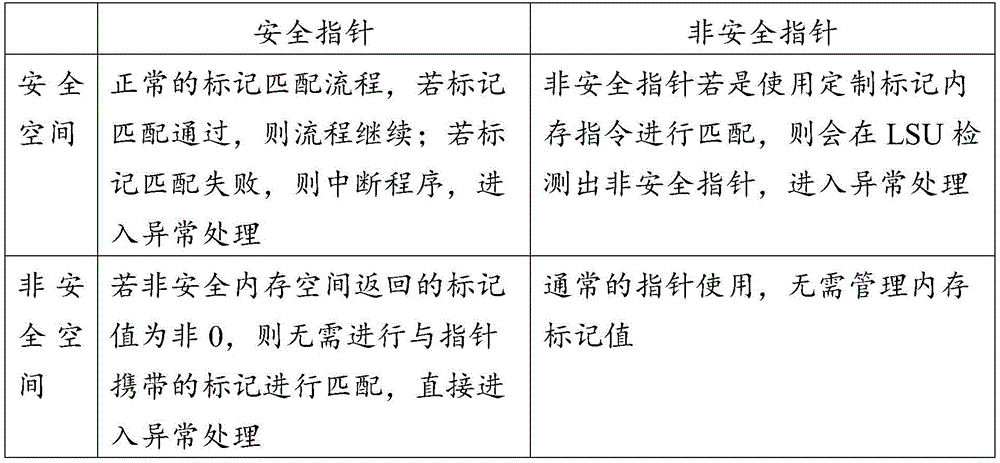
本公开的实施例中仅定义一部分的内存空间为安全内存空间,因此存在安全指针与非安全内存空间、非安全指针与安全内存空间的标记匹配等操作。需要说明的是,在至少一个实施例中,定制的标记内存指令使用内存标记为0的指针访问内存标记为0的安全内存空间时,也同样会触发匹配失败,由此触发硬件异常,这是因为定制的标记内存指令仅针对安全指针地址进行匹配。其余情况如下表2所示。In the embodiments of the present disclosure, only a part of the memory space is defined as the secure memory space, so there are operations such as label matching between the secure pointer and the non-secure memory space, and between the non-secure pointer and the secure memory space. It should be noted that, in at least one embodiment, when a custom marked memory instruction uses a pointer whose memory is marked as 0 to access a secure memory space whose memory is marked as 0, it will also trigger a matching failure, thereby triggering a hardware exception, which is Because custom tag memory instructions only match against safe pointer addresses. The rest of the situation is shown in Table 2 below.
表2Table 2
本公开的至少一个实施例提供了一种处理器或处理器核,处理器可以为包括单个处理器核的单核处理器或包括多个处理器核的多核处理器,以下为了简便起见,将处理器或处理器核统称为“处理器”。本公开实施例的处理器可以用于执行上述标记内存以及对应的操作。图6A示出了上述实施例提供的处理器的框架示意图。At least one embodiment of the present disclosure provides a processor or a processor core. The processor may be a single-core processor including a single processor core or a multi-core processor including multiple processor cores. For simplicity, the following will Processors or processor cores are collectively referred to as "processors." The processor in the embodiment of the present disclosure may be used to execute the above tag memory and corresponding operations. FIG. 6A shows a schematic diagram of the framework of the processor provided in the above embodiment.
如图6A所示,该处理器60包括前端模块61、译码及重命名单元62、发射单元63、寄存器堆64、执行模块65、重排序缓冲器(ROB)66等。As shown in FIG. 6A , the processor 60 includes a front-end module 61 , a decoding and renaming unit 62 , a transmitting
处理器执行应用程序时所使用的地址是虚拟地址。操作系统在给进程分配内存时,需要把使用到的虚拟地址映射到物理地址,物理地址是真正的物理内存访问地址。程序在实际访问内存之前需要先将虚拟地址转换为物理地址。将虚拟地址转换为物理地址的过程被称为地址翻译。处理器使用存储管理单元(MMU)进行地址翻译。并且,为了节省地址翻译的时间,为处理器核提供翻译后备缓冲器(TLB),用于存放一部分之前使用过的页表项(PTE)。当需要进行地址翻译时,首先使用要翻译的虚拟地址查询TLB以看是否有需要的页表项,否则使用要翻译的虚拟地址查询页表来获得需要的页表项,通过页表项和页内地址偏移,就可以获得该要翻译的虚拟地址相对应的物理地址。之后可以使用该物理地址进行访问内存。The addresses used by the processor to execute applications are virtual addresses. When the operating system allocates memory to a process, it needs to map the used virtual address to a physical address, and the physical address is the real physical memory access address. Programs need to convert virtual addresses to physical addresses before actually accessing memory. The process of converting a virtual address to a physical address is called address translation. Processors use a Memory Management Unit (MMU) for address translation. Moreover, in order to save the time of address translation, a translation lookaside buffer (TLB) is provided for the processor core to store a part of previously used page table entries (PTE). When address translation is required, first use the virtual address to be translated to query the TLB to see if there is a required page table entry, otherwise use the virtual address to be translated to query the page table to obtain the required page table entry, through the page table entry and page By using the internal address offset, the physical address corresponding to the virtual address to be translated can be obtained. This physical address can then be used to access memory.
例如,在对带内存标记的虚拟地址进行地址翻译时,首先剥离位于高位的内存标记,使用0填充高位得到修改后的虚拟地址,然后使用修改后的虚拟地址进行地址翻译,或者在不进行内存标记剥离的情况下,仅使用位于低位的有效位进行地址翻译,由此得到翻译后的物理地址,如果需要,再将内存标记与物理地址组合,得到待内存标记的物理地址。For example, when performing address translation on a virtual address with a memory tag, first strip off the high-order memory tag,
这里,前端模块61可以包括取指单元、分支预测单元等(图中未示出),可以与常规的处理器的前端模块相同,这里不赘述。Here, the front-end module 61 may include an instruction fetch unit, a branch prediction unit, etc. (not shown in the figure), which may be the same as front-end modules of a conventional processor, and details will not be described here.
译码及重命名单元62除了对常规的指令进行译码以及对指令中涉及的寄存器进行重命名操作之外,还包括标记内存指令表621,由此可以用于执行对于上述自定义标记内存指令的译码操作,以获得这些标记内存指令对应的微操作码以供后续由执行模块中的执行单元使用。In addition to decoding conventional instructions and renaming the registers involved in the instructions, the decoding and renaming unit 62 also includes a tag memory instruction table 621, which can be used to execute the above-mentioned custom tag memory instructions Decoding operations to obtain the micro-ops corresponding to these marked memory instructions for subsequent use by the execution units in the execution module.
执行模块65包括各种执行单元,例如,访存单元(load/store unit,LSU)651、标记产生单元652、算术逻辑单元(ALU)、乘法单元(MVL)等,分别用于执行访存操作、标记产生操作、算术逻辑运算、乘法运算等。The execution module 65 includes various execution units, for example, a memory access unit (load/store unit, LSU) 651, a label generation unit 652, an arithmetic logic unit (ALU), a multiplication unit (MVL), etc., which are respectively used to perform memory access operations , Flag generation operations, arithmetic logic operations, multiplication operations, etc.
图6B示出根据本公开至少一实施例的标记产生单元的示意图。在本公开的实施例中,如图6B所示,标记产生单元652包括随机数产生子单元6521和标记合格检测子单元6522,用于执行上述IRL、MVL等指令,以产生用于内存标记的标记值。FIG. 6B shows a schematic diagram of a marker generating unit according to at least one embodiment of the present disclosure. In the embodiment of the present disclosure, as shown in FIG. 6B , the mark generation unit 652 includes a random
随机数产生子单元6521例如为随机数生成器,该随机数生成器为硬件乱数生成器(Hardware Random Number Generator,HRNG)。图6C示出根据本公开至少一实施例的硬件乱数生成器的示意图。如图6C所示,例如,在至少一个示例中,硬件乱数生成器包括:基于反相器链的振荡环(COR,Chained Oscillation Ring)、触发器阵列、异或阵列以及输出单元;图6C中输出单元包括四个输出端口[0]~[3]。本公开的实施例对于随机数生成器的实现方式和具体结构没有限定。The random
例如,硬件乱数生成器6521可以具有至少一个随机数生成源,例如两个随机数生成源,这两个随机数生成源分别是COR采用异或门来组合相邻振荡环的抖动信号以及触发器采样时候因为亚稳态的产生的不确定输出。COR电路由于受到工艺、温度、电压等影响,其输出随时间变化具有一定的浮动,处于一种不定态。而且,COR电路输出作为触发器阵列的输入,该输入无法维持触发器正常工作所需要的建立时间以及保持时间,因此触发器最终工作在亚稳态,并且触发器的输出处于非人为控制的随机状态值。硬件乱数生成器的采样点至少包含一个振荡区域,因此输出数据得以保证其随机性。For example, the hardware
标记合格检测子单元6522对硬件乱数生成器6521生成的真随机值进行匹配验证,倘若取得的随机数值为0,则需要重新生成新的随机数,并且再对其进行匹配验证。倘若匹配验证通过,则标记产生单元652则可以发送有效(valid)信号,表示所获得的随机数可用于内存标记。前述匹配验证确保了不会产生为零(0)的内存标记,也即内存标记都是非0的,由此使得非带有内存标记的(非安全)内存地址与内存地址的有效部分与内存标记整合为一体时的(安全)内存地址相区别。更进一步地,在至少一个示例中,标记合格检测子单元6522除了如上所述检测标记是否为0之外,还检测所生成的标记是否各位都为1,如果是,则也设定为匹配验证不通过。The flag qualified detection subunit 6522 performs matching verification on the true random value generated by the hardware
在本公开至少一个实施例中,访存单元(LSU)651除了具有用于执行常规的针对非安全内存空间的访存指令,以从目标地址读取数据或将数据写入目标地址等之外,该访存单元651可以访问一级(L1)数据缓存67和二级(L2)缓存68等。访存指令用于在内存和寄存器之间传递数据,例如用于执行读取(Load)和存储(Store)操作,例如RISC-V中常规的访存指令包括lw指令与sw指令、lb指令与sb指令等。In at least one embodiment of the present disclosure, the memory access unit (LSU) 651 is used to execute conventional memory access instructions for non-secure memory space, to read data from the target address or write data to the target address, etc. , the
在本公开的实施例中,该访存单元651还用于执行本公开实施例中上述自定义LDL指令、SDL指令、SDDL指令等,分别用于获取目标地址的内存标记,或将内存标记写入与目标地址对应的标记项中等,用于将数据存入目标地址对应的标记内存中等。In the embodiment of the present disclosure, the
本公开至少一个实施例的处理器对于指令的执行方式可以是顺序执行,也可以是乱序执行。乱序执行过程中,处理器允许将多条指令不按取指顺序而将指令分开发送给各相应执行单元处理。重排序缓冲器(ROB)提供来使得乱序执行的指令被顺序地提交。具体而言,一条指令在经过译码和重命名之后,就会被派遣到ROB中、进入发射单元(发射队列)中,并且其状态被标记为“正在执行中”;在该指令被执行完毕后,ROB会被通知并将该指令的状态标记为“执行完毕”;之后,当该指令在ROB中位置被移位到ROB的头部时,该指令会被提交(这里的“提交”指的是修改处理器状态,如修改逻辑寄存器堆),这条指令的结果在外部将可以被“观测”到。即,ROB记录下各条指令在当前执行的程序中的顺序,并且一条指令在执行完毕之后不会立刻提交,而是先在ROB中等待,等到其前面的所有指令都提交完毕,才可以提交结果到寄存器堆。例如,在处理器核(例如BOOM处理器核)的处理流水线中,重排序缓冲器(ROB)的每个条目(Entry)中,通过例如如下几个状态寄存器记录着该条目的状态,例如这些状态寄存器包括(但不限于):The execution mode of the processor in at least one embodiment of the present disclosure may be sequential execution or out-of-order execution. In the process of out-of-order execution, the processor allows multiple instructions to be sent separately to each corresponding execution unit for processing without following the instruction fetch order. A reorder buffer (ROB) is provided so that instructions executed out of order are committed sequentially. Specifically, after an instruction is decoded and renamed, it will be dispatched to the ROB, enter the launch unit (launch queue), and its status will be marked as "executing"; after the instruction is executed Afterwards, the ROB will be notified and mark the status of the instruction as "execution completed"; later, when the position of the instruction in the ROB is shifted to the head of the ROB, the instruction will be submitted (the "commit" here refers to The purpose is to modify the processor state, such as modifying the logical register file), and the result of this instruction will be "observed" externally. That is, ROB records the order of each instruction in the currently executing program, and an instruction will not be submitted immediately after execution, but will wait in ROB first, and can only be submitted after all previous instructions are submitted. The result goes to the register file. For example, in the processing pipeline of a processor core (such as a BOOM processor core), in each entry (Entry) of the reordering buffer (ROB), the state of the entry is recorded through, for example, the following status registers, such as these Status registers include (but are not limited to):
val(valid):该条目是否有效;val(valid): whether the entry is valid;
bsy(busy):该条目的指令是否在执行中;bsy(busy): whether the command of this entry is being executed;
exc(exception):该条目是否是一个异常;exc(exception): whether the entry is an exception;
br_mask:该条目的指令属于哪个处于预测中的分支上。br_mask: The instruction of this entry belongs to which branch is in prediction.
本公开的至少一个实施例提供了一种计算机装置,该计算机装置包括上述处理器以及与该处理器配合的多级缓存。图7示出了该实施例的计算机装置的示意图。如图7所示,计算机装置700包括至少一个处理器(或处理器核)710、一级缓存(L1缓存)、二级缓存(L2缓存)730、内存740和标记存储750。一级缓存(L1缓存)可以划分为例如彼此独立的一级指令缓存(L1指令缓存)721和一级数据缓存(L1数据缓存)722;二级缓存730统一用于指令和数据,而不进行划分。例如,内存740采用DRAM而标记存储750采用SRAM。如下面具体描述的实施例,L1数据缓存和L2缓存还包括用于处理内存标记的部分(图中用L表示)。At least one embodiment of the present disclosure provides a computer device, which includes the above-mentioned processor and a multi-level cache cooperating with the processor. FIG. 7 shows a schematic diagram of the computer device of this embodiment. As shown in FIG. 7 , a
该处理器710包括存储管理单元(MMU)711和翻译后备缓冲器(TLB)712,以用于执行对于内存地址的地址翻译,以将虚拟地址翻译为对应的物理地址。The processor 710 includes a Memory Management Unit (MMU) 711 and a Translation Lookaside Buffer (TLB) 712 for performing address translation on memory addresses, so as to translate virtual addresses into corresponding physical addresses.
本公开的实施例对于处理器(或处理器核)的架构不做限制,例如可以为用于RISC-V指令集、ARM指令集的微架构,例如对于用于RISC-V指令集的微架构,可以为BOOM处理器核(例如SonicBoom处理器核)等。在上述计算机装置中,一级缓存和二级缓存之间通过总线701连接;二级缓存和内存、标记存储之间也通过总线701连接。该总线701例如为TileLink总线。TileLink总线支持缓存一致性协议。Embodiments of the present disclosure do not limit the architecture of the processor (or processor core), for example, it may be a microarchitecture for RISC-V instruction set, ARM instruction set, for example, for a microarchitecture for RISC-V instruction set , may be a BOOM processor core (such as a SonicBoom processor core) and the like. In the above computer device, the L1 cache and the L2 cache are connected through the bus 701 ; the L2 cache is also connected with the internal memory and tag storage through the bus 701 . The bus 701 is, for example, a TileLink bus. The TileLink bus supports the cache coherence protocol.
在本公开的实施例中,例如上述LDL和SDL指令要分别从标记存储750读取内存标记以及在标记存储750中写入内存标记,同样地,为了加快对于内存标记的处理,需要在上述多级缓存中提供对于内存标记的缓存,例如将内存标记作为数据的一种加以处理。然而,如前所述,内存标记本身的大小(LS)可以选择为少于1个字节(例如5个位或6个位),则内存标记的大小与缓存行(或称为“缓存块”)的大小不能对齐,而且内存标记的存储地址(标记项的存储地址)与安全内存空间编址方式可能不同,因此需要修改对于L1缓存和L2缓存的常规访问逻辑,这将导致系统实现变得复杂。In the embodiment of the present disclosure, for example, the above-mentioned LDL and SDL instructions need to read the memory tag from the
本公开的至少一个实施例提供了一种用于计算机装置的缓存,该缓存与处理器配合工作,可以用于一级缓存、二级缓存等。At least one embodiment of the present disclosure provides a cache for a computer device. The cache cooperates with a processor and can be used for a first-level cache, a second-level cache, and the like.
根据本公开的至少一实施例提供的缓存,该缓存包括数据阵列、标签阵列和标记阵列。该数据阵列配置为用于存储多个缓存行;该标签阵列配置为用于存储多个标签;该标记阵列配置为用于存储多个标记行。多个缓存行、多个标签以及多个标记行彼此一一对应,每个标记行用于存储与对应的缓存行中存储的第一数量的标记存储单元项相关联的第二数量的内存标记,标记行中存储的内存标记与关联的标记存储单元项的内存地址具有映射关系。通过该关联关系,内存标记可以对关联的标记存储单元项的访问提供验证、保护。例如,第一数量和第二数量可以相同或不同。According to the cache provided by at least one embodiment of the present disclosure, the cache includes a data array, a tag array and a tag array. The data array is configured to store multiple cache lines; the tag array is configured to store multiple tags; and the tag array is configured to store multiple tag lines. A plurality of cache lines, a plurality of tags, and a plurality of tag rows are in one-to-one correspondence with each other, and each tag row is used to store a second number of memory tags associated with the first number of tag storage unit items stored in the corresponding cache line , the memory tag stored in the tag row has a mapping relationship with the memory address of the associated tag storage unit item. Through this association relationship, the memory tag can provide verification and protection for the access of the associated tag storage unit item. For example, the first quantity and the second quantity may be the same or different.
在本公开的至少一实施例中,例如,数据阵列、标签阵列和标记阵列具有相同的逻辑组织结构。In at least one embodiment of the present disclosure, for example, the data array, tag array, and tag array have the same logical organization structure.
在本公开的至少一实施例中,上述缓存还包括至少一个地址译码器,该至少一个地址译码器配置为根据输入到缓存的访存地址中记载的索引对数据阵列、标签阵列和标记阵列进行检索,以确定数据阵列、标签阵列和标记阵列中的目标缓存行、目标标签和目标标记行。In at least one embodiment of the present disclosure, the cache further includes at least one address decoder configured to perform an index on the data array, the tag array, and the tag according to the index recorded in the access address input to the cache. array to determine the target cache line, target tag, and target tag line in the data array, tag array, and tag array.
在本公开的至少一实施例中,该至少一个地址译码器包括第一地址译码器和第二地址译码器,第一地址译码器根据索引对数据阵列和标记阵列进行检索,以确定目标缓存行所在的目标缓存行组和目标标记行所在的目标标记行组,第一地址译码器根据索引对标签阵列进行检索以确定目标标签所在的目标标签组。In at least one embodiment of the present disclosure, the at least one address decoder includes a first address decoder and a second address decoder, and the first address decoder searches the data array and the tag array according to the index, so as to The target cache line group where the target cache line is located and the target tag line group where the target tag line is located are determined, and the first address decoder searches the tag array according to the index to determine the target tag group where the target tag line is located.
在本公开的至少一实施例中,上述缓存还包括比较器、第一多路选择器和第二多路选择器。该比较器配置为根据输入到缓存的访存地址中记载的标签与目标标签组比较以确定是否命中,并且响应于该命中,提供访存地址中记载的标签在目标标签组中的路编号;第一多路选择器配置为根据路编号,从目标缓存行组输出目标缓存行;第二多路选择器配置为根据路编号,从目标标记行组输出目标标记行。In at least one embodiment of the present disclosure, the cache further includes a comparator, a first multiplexer, and a second multiplexer. The comparator is configured to compare the tag recorded in the memory access address input to the cache with the target tag group to determine whether it is a hit, and in response to the hit, provide the way number of the tag recorded in the memory access address in the target tag group; The first multiplexer is configured to output the target cache line from the target cache line group according to the way number; the second multiplexer is configured to output the target tag line from the target tag line group according to the way number.
在本公开的至少一实施例中,上述缓存还包括第一校准器和第二校准器。第一校准器配置为根据输入到缓存的访存地址中记载的偏移从目标缓存行中选择目标数据项;第二校准器配置为根据输入到缓存的访存地址中记载的偏移从目标标记行中选择目标标记项。In at least one embodiment of the present disclosure, the cache further includes a first calibrator and a second calibrator. The first aligner is configured to select the target data item from the target cache line according to the offset recorded in the access address input to the cache; the second aligner is configured to select the target data item from the target cache line according to the offset recorded in the access address input to the cache. Select the target tag item in the tag row.
在本公开的至少一实施例中,上述缓存还包括匹配检测器,该匹配检测器配置为将输入到缓存的访存地址中记载的第一内存标记与目标标记项记载的第二内存标记进行比较,以确定第一内存标记和第二内存标记是否匹配。In at least one embodiment of the present disclosure, the cache further includes a match detector configured to compare the first memory tag recorded in the access address input to the cache with the second memory tag recorded in the target tag entry Compare to determine if the first memory tag and the second memory tag match.
在本公开的至少一实施例中,上述缓存还包括数据缓冲器和标记缓冲器;该数据缓冲器配置为保存目标数据项;该标记缓冲器配置为保存目标标记项。In at least one embodiment of the present disclosure, the cache further includes a data buffer and a tag buffer; the data buffer is configured to store the target data item; the tag buffer is configured to store the target tag item.
在本公开的至少一实施例中,上述缓存还包括缺失状态处理寄存器,该缺失状态处理寄存器配置为当缓存处理的访问请求导致缓存缺失时,记录缓存缺失,且当缓存缺失被处理后,释放被记录的缓存缺失。In at least one embodiment of the present disclosure, the above-mentioned cache further includes a missing state processing register, and the missing state processing register is configured to record a cache miss when an access request processed by the cache causes a cache miss, and release the cache miss after the cache miss is processed. Logged cache misses.
在本公开的至少一实施例中,上述缓存还包括请求缓冲器,该请求缓冲器配置为临时存储缓存接收的访存请求,以等待缓存处理访存请求。In at least one embodiment of the present disclosure, the cache further includes a request buffer configured to temporarily store memory access requests received by the cache, so as to wait for the cache to process the memory access requests.
在本公开的至少一实施例中,请求缓冲器还配置为用于对涉及数据的访存请求的处理,以及用于对涉及内存标记的访存请求的处理。In at least one embodiment of the present disclosure, the request buffer is further configured for processing memory access requests involving data, and for processing memory access requests involving memory tags.
在本公开的至少一实施例中,上述缓存还包括响应缓冲器,该响应缓冲器配置为临时存储缓存对于访存请求出现缓存缺失的情况下接收对对访存请求的响应,以等待缓存对于响应的处理。In at least one embodiment of the present disclosure, the above-mentioned cache further includes a response buffer configured to temporarily store the response to the memory access request when the cache misses the memory access request, so as to wait for the cache to respond to the memory access request. The processing of the response.
在本公开的至少一实施例中,该响应缓冲器还配置为用于对涉及数据的访存请求的处理,以及用于对涉及内存标记的访存请求的处理。In at least one embodiment of the present disclosure, the response buffer is also configured to process memory access requests involving data, and to process memory access requests involving memory tags.
在本公开的至少一实施例中,上述缓存还包括至少一个接口单元,该至少一个接口单元配置为用于缓存与处理器或其他缓存进行通信。In at least one embodiment of the present disclosure, the cache further includes at least one interface unit configured for the cache to communicate with a processor or other caches.
在本公开的至少一实施例中,上述缓存还包括控制单元,该控制单元配置为:接收访存请求,其中,该访存请求包括访存地址,访存地址包括第一内存标记;响应于使用访存地址查询缓存命中的情况下,从标记阵列获取对应于访存地址的第二内存标记;比较获取的第一内存标记和获取的第二内存标记以确定第一内存标记和第二内存标记是否匹配。In at least one embodiment of the present disclosure, the cache further includes a control unit configured to: receive a memory access request, wherein the memory access request includes a memory access address, and the memory access address includes a first memory tag; in response to In the case of using the access address to query the cache hit, obtain the second memory tag corresponding to the access address from the tag array; compare the obtained first memory tag and the obtained second memory tag to determine the first memory tag and the second memory tag Whether the tag matches.
本公开的至少一个实施例还提供一种计算机装置,该计算机装置包括处理器、至少一缓存和内存。该至少一缓存采用上述任一实施例的缓存;该处理器与上述至少一缓存耦接;内存与处理器和缓存耦接且配置为在计算机装置的运行过程中提供内存空间,其中,所述缓存所涉及的内存地址位于内存空间中。At least one embodiment of the present disclosure further provides a computer device, which includes a processor, at least one cache and memory. The at least one cache adopts the cache in any of the above-mentioned embodiments; the processor is coupled to the at least one cache; the memory is coupled to the processor and the cache and is configured to provide memory space during the operation of the computer device, wherein the The memory addresses referred to by the cache are located in the memory space.
在本公开的至少一实施例中,上述至少一缓存包括一级缓存和二级缓存。In at least one embodiment of the present disclosure, the at least one cache includes a first-level cache and a second-level cache.
在本公开的至少一实施例中,一级缓存和二级缓存之间通过总线连接,该总线在计算机装置的运行过程中具有传送当前事务是否为内存标记相关事务的标志位。In at least one embodiment of the present disclosure, the L1 cache and the L2 cache are connected through a bus, and the bus has a flag bit for transmitting whether the current transaction is a memory tag related transaction during the operation of the computer device.
在本公开的至少一实施例中,该计算机装置还包括标记存储,该标记存储与处理器和内存耦接,且配置为用于存储多个内存标记,其中,标记存储中存储的多个内存标记分别与内存空间中分配的多个内存地址具有映射关系。In at least one embodiment of the present disclosure, the computer device further includes a tag storage, the tag storage is coupled to the processor and the memory, and is configured to store a plurality of memory tags, wherein the plurality of memory tags stored in the tag storage The tags respectively have a mapping relationship with multiple memory addresses allocated in the memory space.
在本公开的至少一实施例的计算机装置中,该处理器包括标记产生单元,该标记产生单元配置为计算机装置的运行过程中根据输入处理器的指令产生用于内存标记的随机值。In the computer device of at least one embodiment of the present disclosure, the processor includes a flag generating unit configured to generate a random value for a memory flag according to an instruction input to the processor during operation of the computer device.
本公开的至少一个实施例还提供一种上述缓存的操作方法,该操作方法包括:接收访存请求,其中,访存请求包括访存地址,访存地址包括第一内存标记;响应于使用访存地址查询缓存命中的情况下,从标记阵列获取对应于访存地址的第二内存标记;比较获取的第一内存标记和获取的第二内存标记以确定第一内存标记和第二内存标记是否匹配。At least one embodiment of the present disclosure further provides an operation method of the above-mentioned cache, the operation method includes: receiving a memory access request, wherein the memory access request includes a memory access address, and the memory access address includes a first memory tag; In the case of a memory address query cache hit, the second memory tag corresponding to the memory access address is obtained from the tag array; the first memory tag obtained and the second memory tag obtained are compared to determine whether the first memory tag and the second memory tag are match.
图8示出了根据本公开一实施例的缓存的示意图。如图8所示,该缓存80包括数据阵列(data array)81、标签阵列(tag array)82和标记阵列(label array)83。Fig. 8 shows a schematic diagram of a cache according to an embodiment of the present disclosure. As shown in FIG. 8 , the cache 80 includes a data array (data array) 81 , a tag array (tag array) 82 and a label array (label array) 83 .
在该实施例的一个示例中,这三个阵列具有相同的逻辑组织结构并且彼此对应,例如,对于数据阵列中的每一项,在标签阵列中存在对应的一项,在标记阵列中存在对应的一项。例如,数据阵列的逻辑组织结构可以是直接相联映射、分组相联映射或全相联映射方式,则对应地,标签阵列82和标记阵列83可以是直接相联映射、分组相联映射或全相联映射方式。In one example of this embodiment, the three arrays have the same logical organization structure and correspond to each other, for example, for each item in the data array, there is a corresponding item in the tag array, and there is a corresponding item in the tag array. of an item. For example, the logical organization structure of the data array can be direct associative mapping, group associative mapping or full associative mapping, then correspondingly, label array 82 and tag array 83 can be direct associative mapping, grouping associative mapping or full associative mapping. Associative mapping method.
在下面说明中以分组相联映射为例进行说明。本公开的实施例对于分组相联映射的结构不做具体限制,例如,每组(set)可以包括2路(way)、4路等。如图8示出了对于2路组的逻辑组织结构,数据阵列中每组具有两个缓存行(例如,缓存行811、812),分别对应于2路W1和W2;相应地,每个标签组具有两个标签(例如,标签821、822),分别对应于2路W1和W2以及分别对应于两个缓存行(例如,缓存行811、812);相应地,每个标记行具有两个内存标记行(例如,标记行831、832),分别对应于2路W1和W2以及分别对应于两个缓存行(例如,缓存行811、812)。In the description below, group associative mapping is taken as an example for illustration. Embodiments of the present disclosure do not specifically limit the structure of the packet associative mapping, for example, each set (set) may include 2 ways, 4 ways, and so on. Figure 8 shows the logical organizational structure for 2-way groups, each group in the data array has two cache lines (for example, cache lines 811, 812), corresponding to 2-way W1 and W2 respectively; correspondingly, each label The set has two tags (e.g., tags 821, 822) corresponding to 2-way W1 and W2 respectively and two cache lines (e.g., cache lines 811, 812); correspondingly, each tag line has two Memory tag lines (eg,
例如,缓存行的大小可以为32字节或64字节,内存中的内存行(memory block)相应地也是32字节或64字节,并且安全内存空间中安全内存子空间与内存行对齐。根据标记内存的标记粒度(LG)的大小,标记阵列中每个标记行中内存标记的数量则可能不同;例如,当缓存行的大小为64字节,且安全内存空间的标记粒度也为64字节时,则每个缓存行存储了1个安全内存子空间对应的标记存储单元项(即具有标记粒度大小的内存空间),对应地每个标记行中仅包括1个内存标记;当缓存行的大小为64字节,而标记粒度为32字节时,则每个缓存行存储了2个安全内存子空间对应的标记存储单元项,对应地每个标记行中包括2个内存标记,分别对应于相应的缓存行中前32个字节的标记存储单元项和后32个字节对应的标记存储单元项。For example, the size of a cache line can be 32 bytes or 64 bytes, and a memory block in the memory is also 32 bytes or 64 bytes accordingly, and the secure memory subspace in the secure memory space is aligned with the memory block. Depending on the tag granularity (LG) of the tagged memory, the number of memory tags in each tag row in the tag array may vary; for example, when the size of the cache line is 64 bytes and the tag granularity of the secure memory space is also 64 Bytes, each cache line stores a tag storage unit item corresponding to a secure memory subspace (that is, a memory space with a tag granularity size), and correspondingly only includes one memory tag in each tag line; when the cache When the line size is 64 bytes and the tag granularity is 32 bytes, each cache line stores two tag storage unit items corresponding to the secure memory subspace, correspondingly, each tag row includes two memory tags, The tag storage unit items corresponding to the first 32 bytes in the corresponding cache line and the tag storage unit items corresponding to the last 32 bytes respectively.
在该实施例的另一个示例中,数据阵列和标签阵列具有相同的逻辑组织结构,然而标记阵列与数据阵列不具有相同的逻辑组织结构但仍彼此对应,例如,对于数据阵列中的每一项,在标签阵列中存在对应的一项,在标记阵列中存在对应的一项。例如,数据阵列81的逻辑组织结构是分组相联映射,而标记阵列83的逻辑组织结构可以采用直接相联映射方式。标记阵列中每一标记行对应于数据阵列中的一组,且每一标记行仅包括1个内存标记,在这种情况下,标记粒度的大小等于缓存行的大小×路(way)所得到的大小,例如,当缓存行的大小为64字节且数据阵列81采用2路组的逻辑组织结构,则标记粒度为64*2,即128字节,即数据阵列中同一组中的两个缓存行都被映射为同一内存标记,此时每个缓存行存储了1/2个标记存储单元项。在该实施例中,标记阵列83的逻辑组织结构可以采用分组相联映射方式,只是组中多个标记行彼此相同。In another example of this embodiment, the data array and the label array have the same logical organization structure, however the label array and the data array do not have the same logical organization structure but still correspond to each other, for example, for each item in the data array , there is a corresponding item in the labels array and a corresponding item in the tags array. For example, the logical organization structure of the data array 81 is group-associative mapping, while the logical organization structure of the tag array 83 may adopt a direct associative mapping method. Each tag line in the tag array corresponds to a group in the data array, and each tag row includes only one memory tag. In this case, the size of the tag granularity is equal to the size of the cache line × way (way) For example, when the size of the cache line is 64 bytes and the data array 81 adopts the logical organization structure of 2-way group, the marking granularity is 64*2, that is, 128 bytes, that is, two in the same group in the data array The cache lines are all mapped to the same memory tag, and each
如上所述,在本公开的不同的实施例中,缓存行中存储的标记存储单元项的数量(第一数量)与标记行存储的标记项(内存标记)的数量(第二数量)相同或不同。As mentioned above, in different embodiments of the present disclosure, the number of tag storage unit items stored in the cache line (the first number) is the same as the number of tag items (memory tags) stored in the tag line (the second number) or different.
图9示出了根据至少一实施例的示例性缓存的结构,该缓存90包括数据阵列91、标签阵列92和标记阵列93,例如,如上所述这三者都具有分组相联映射的逻辑组织结构,或者数据阵列91和标签阵列92具有分组相联映射的逻辑组织结构而标记阵列93具有直接相邻映射。该缓存90还包括两个地址译码器941和942、两个多路选择器(Mux)951和952、两个校准器(Aligner)961和962、比较器98、匹配检测器(Check)99。Figure 9 shows the structure of an exemplary cache according to at least one embodiment, the
地址译码器941用于数据阵列91和标记阵列93,地址译码器942用于标签阵列92,这两个地址译码器对同一个输入(即下面描述的索引)进行译码。在其他示例中,这两个地址译码器也可以被合并为单个地址译码器,该单个地址译码器将译码输出同时提供给数据阵列、标签阵列和标记阵列。地址译码器941和942根据输入到缓存90的访存地址中记载的索引对数据阵列、标签阵列和标记阵列进行检索,以确定数据阵列、标签阵列和标记阵列中的目标缓存行、目标标签和目标标记行。更具体而言,地址译码器941根据索引对数据阵列和标记阵列进行检索,以确定目标缓存行所在的目标缓存行组和目标标记行所在的目标标记行组;地址译码器942根据索引对标签阵列进行检索以确定目标标签所在的目标标签组。The address decoder 941 is used for the
比较器98用于将输入的访存地址中本身记载的标签(tag)与根据输入(即索引)从标签阵列检索得到的目标标签组中的多个标签分别比较,从而确定是否缓存命中(CacheHit)或缓存缺失(Cache Miss),如果缓存命中,则提供访存地址中记载的标签在目标标签组中的路编号(例如图8所示的路W1或路W2)。The
多路选择器951用于数据阵列91,以根据输入的选择信号(即上述路编号)从数据阵列91的目标缓存行组输出目标缓存行;多路选择器952用于标记阵列93,以根据输入的选择信号(即上述路编号)从标记阵列93的目标标记行组输出目标标记行。The multiplexer 951 is used in the
校准器961用于数据阵列91,以在数据阵列91中选择的目标缓存行中再根据访存地址中记载的偏移进行选择,以获得目标数据项,选择结果被存入数据缓冲器(DataBuffer)971;校准器962用于标记阵列93,以在标记阵列93中选择的目标标记行中再根据偏移进行选择,以获得目标标记项,选择结果被存入标记缓冲器(Label Buffer)972。The calibrator 961 is used for the
由于缓存行与标记行的组织方式一定相同,因此校准器961和校准器962对于偏移的使用方式不一定相同。例如,在一个示例中,缓存行的大小为64字节(在64位系统中包括8个字),安全内存空间的标记粒度也为64字节,每个缓存行存储了1个标记存储单元项,对应地每个标记行中仅包括1个内存标记,当指令集(ISA)是基于字寻址时(例如目标数据项的大小为字),那么可以使用偏移在缓存行中再定位8个字之一以得到目标数据项,而此时标记行中仅有一个内存标记,因此实际无需使用偏移。又例如,在另一个示例中,缓存行的大小为64字节,而标记粒度为32字节,每个缓存行存储了2个标记存储单元项,对应地每个标记行中包括2个内存标记,那么可以使用偏移在缓存行中再定位8个字之一以得到目标数据项,在标记行中再定位2个内存标记之一以得到目标标记项。Since the cache line and tag line must be organized in the same way, the aligner 961 and aligner 962 do not necessarily use the same offset. For example, in one example, the size of the cache line is 64 bytes (comprising 8 words on a 64-bit system), the tag granularity of the secure memory space is also 64 bytes, and each
匹配检查器99用于将输入的访存地址中本身记载的内存标记(label)与根据输入(即索引)从标记阵列检索得到的目标标记项记载的内存标记(即保存在标记缓冲器中的内存标记)比较,从而确定二者是否匹配。The matching checker 99 is used to record the memory label (label) recorded in the access memory address of the input and the memory label recorded in the target label item that is retrieved from the label array according to the input (ie index) (that is, the label stored in the label buffer) memory tag) to determine whether the two match.
该缓存90还包括控制模块(或控制逻辑,图中未示出),该控制模块配置为用于控制该缓存空间的操作,这些操作例如包括:接收访存请求,其中,该访存请求包括访存地址,访存地址包括第一内存标记;响应于使用访存地址查询缓存命中的情况下,从标记阵列获取对应于访存地址的第二内存标记;比较获取的第一内存标记和获取的第二内存标记以确定第一内存标记和第二内存标记是否匹配。The
进一步地,在本公开实施例的上述缓存,还需要能够区分带内存标记的指令和正常的指令(即不带内存标记的指令),由此实现与内存标记相应的操作,例如,标记匹配、匹配失败后异常报告等。需要指出的是,本公开实施例的缓存当然也能够执行正常的指令。Further, in the above-mentioned cache in the embodiment of the present disclosure, it is also necessary to be able to distinguish instructions with memory tags from normal instructions (ie, instructions without memory tags), thereby implementing operations corresponding to memory tags, for example, tag matching, Exception report after matching failure, etc. It should be noted that, of course, the cache in the embodiments of the present disclosure can also execute normal instructions.
本公开实施例的缓存还可以根据需要包括其他电路部分,这些电路部分例如包括有效位阵列、对于二级缓存的预取(prefetch)单元、目录组织等,例如,有效位阵列对应于标签阵列,用于记载对应的缓存行是否有效(valid)(例如:1代表有效;0代表无效)。只有在某个缓存行有效的情况下,比较标签才有意义;如果无效,可以直接判定缓存缺失。本公开的实施例对其他电路部分的组成、功能等不作限制,因此不再赘述。The cache in the embodiments of the present disclosure may also include other circuit parts as required, and these circuit parts include, for example, valid bit arrays, prefetch units for L2 cache, directory organization, etc. For example, the valid bit arrays correspond to tag arrays, It is used to record whether the corresponding cache line is valid (for example: 1 means valid; 0 means invalid). Comparing tags is only meaningful if a cache line is valid; if it is invalid, it can be directly determined that the cache is missing. The embodiments of the present disclosure do not limit the composition, functions, etc. of other circuit parts, so details will not be repeated here.
对于缓存的访问采用的是虚拟地址经地址翻译后得到的物理地址。对于操作标记内存的指令,在将带内存标记的虚拟地址翻译之后,将翻译得到的物理地址以及从虚拟地址高位剥离得到的内存标记一起(例如将二者结合得到带内存标记的物理地址)提供给缓存。因此,用于内存访问的被标记的访存地址进入缓存时会被分为标签(tag)、索引(index)、偏移(offset)以及标记(label)这四部分(前三者来自翻译得到的物理地址):The access to the cache uses the physical address obtained by address translation of the virtual address. For instructions that operate marked memory, after translating the virtual address with memory mark, the translated physical address and the memory mark stripped from the high bit of the virtual address are provided together (for example, combining the two to obtain the physical address with memory mark) to cache. Therefore, when the marked access address for memory access enters the cache, it will be divided into four parts: tag, index, offset, and label (the first three are obtained from the translation physical address):
·偏移(offset)被用来识别访存地址对应的目标数据项以及目标标记项分别存储在缓存行或标记行中的哪一个字或字节(这取决于处理器所采用的指令集(ISA)是基于字寻址的还是基于字节寻址的);The offset (offset) is used to identify which word or byte in the cache line or tag line the target data item corresponding to the memory access address and the target tag item are stored in (this depends on the instruction set used by the processor ( ISA) is word-based or byte-based);
·索引(index)用来决定目标缓存行、目标标签和目标标记行存储在哪个组(set)中或是应当从哪个组(set)中查找;The index (index) is used to determine which set (set) the target cache line, target tag and target tag line are stored in or should be looked up from;
·标签(tag)用来与标签阵列的目标标签组中储存的多个标签比较,决定访问请求是否缓存命中(hit)以及在命中的情况下是在当前组(set)中哪一路(way)命中;The tag (tag) is used to compare with multiple tags stored in the target tag group of the tag array to determine whether the access request is a cache hit (hit) and in the case of a hit, which way (way) in the current set (set) hit;
·标记(label)用来在缓存命中的情况下,与从标记阵列中对应于数据阵列中被选择的访存地址的数据项的内存标记项记载的内存标记进行匹配、比较。The label (label) is used to match and compare with the memory label recorded in the memory label item of the data item corresponding to the selected memory access address in the data array in the label array in the case of a cache hit.
参考图9所示,如上所述,当处理器执行一条访存指令的过程中,例如,在执行读取指令而需要访问缓存时,访存指令使用了被标记的访存地址以对安全内存空间进行访问,该被标记的访存地址在进行了地址翻译之后得到带标记的物理地址,该带标记的物理地址进入缓存时被拆分为标记(label)、标签(tag)、索引(index)、偏移(offset),标记被送入匹配检查器99,标签被输入比较器98,索引被送入地址译码器941和地址译码器942;偏移被送入校准器961和校准器962。As shown in FIG. 9 , as described above, when the processor executes a memory access instruction, for example, when executing a read instruction and needs to access the cache, the memory access instruction uses the marked memory access address to secure memory The marked physical address is obtained after address translation, and the marked physical address is split into a label, a tag, and an index when it enters the cache. ), offset (offset), the mark is sent into the matching checker 99, the label is sent into the
如上所述,地址译码器411和地址译码器9422进行对索引进行译码,得到在数据阵列91、标签阵列92和标记阵列93中分别需要选择的组(set);数据阵列91和标记阵列93中各自被选中的组的内容被分别送入多路选择器951和多路选择器952,标签阵列92中被选中的组的内容被分别送入比较器98,比较器将访存地址本身的标签与标签阵列92中被选中的组中的多个标签分别进行比较之后,如果比较器98确定访存地址中本身的标签与标签阵列92中被选中的组中的某个标签相同(即缓存命中),则在命中的情况下将被命中的标签所在路的路编号输出,且比较器98将该路编号送入多路选择器951和多路选择器952作为选择信号,如果不同(即缓存缺失),则返回缺失信号。As mentioned above, the address decoder 411 and the address decoder 9422 decode the index to obtain the groups (set) that need to be selected respectively in the
在比较器确定命中的情况下,多路选择器951和多路选择器952根据比较器输出的选择信号(即路编号),选择数据阵列91和标记阵列93中各自被选中的组中相应路中的缓存行以及标记行输出,并分别对应输出至校准器961和校准器962。When the comparator determines a hit, the multiplexer 951 and the multiplexer 952 select the corresponding way in the selected group in the
校准器961和校准器962根据该偏移在多路选择器1和多路选择器2输出的缓存行和标记行中分别选择目标数据项和目标标记项,并将它们分别存入数据缓冲器971和标记缓冲器972。The calibrator 961 and the calibrator 962 respectively select the target data item and the target tag item in the cache line and the tag line output by the
匹配检查器99将接收的标记(label)与保存在标记缓冲器972中的标记进行比较,确定二者是否匹配,在匹配的情形,向处理器反馈匹配成功的信号,否则在不匹配的情形,反馈匹配失败的信号。处理器根据匹配成功的信号,读取在数据缓冲器971的数据项,否则根据匹配失败的信号,进入异常处理。Matching checker 99 compares the label (label) received with the label stored in the label buffer 972 to determine whether the two match, and in the case of matching, a signal of successful matching is fed back to the processor, otherwise in the case of no match , feedback signal of matching failure. The processor reads the data items in the data buffer 971 according to the signal of matching success, or enters into exception processing according to the signal of matching failure.
本公开实施例的缓存兼容常规的非标记的访存地址的访存操作,非标记的访存地址不具有标记部分,因此相应地,缓存中的标记阵列93、多路选择器952、校准器962、标记缓冲器972、匹配检查器99不被激活,从而不参与缓存处理。并且,在上述缓存的使用过程中,使用最近访问的数据以填充缓存的数据阵列的多个项时所采用的替换策略可以包括最近使用(Least Recently Used,LRU)、最不常使用(Least-Frequently Used,LFU)等,对应地,对于填充缓存的标记阵列的多个项时也采用相同的策略,本公开的实施例对具体采用的策略不作限制。The cache of the embodiment of the present disclosure is compatible with the memory access operation of the conventional non-marked memory access address, and the non-marked memory access address does not have a mark part, so correspondingly, the
并且,在执行存储(store)指令而需要写缓存时,例如可以采用多种写策略,包括直写(write through)、后写(post write)以及写回(write back)等方式。其中,在直写方式中,处理器向缓存写入数据时,同时向内存也写一份,使得缓存和内存的数据保持一致;在后写方式中,处理器更新缓存数据时,把更新的数据写入到一个更新缓冲器,在合适的时候才将更新的数据写入内存中,对内存进行更新;在写回方式中,处理器向缓存写入数据时,更新的数据仅被写入到缓存中,之后只有当修改过的缓存行被替换时才被写到内存中。Moreover, when a write cache is required for executing a store instruction, for example, various write strategies may be adopted, including write through, post write, and write back. Among them, in the write-through mode, when the processor writes data to the cache, it also writes a copy to the memory at the same time, so that the data in the cache and the memory are consistent; in the write-behind mode, when the processor updates the cache data, the updated The data is written into an update buffer, and the updated data is written into the memory at an appropriate time to update the memory; in the write-back mode, when the processor writes data to the cache, the updated data is only written to the cache, and then only written to memory when the modified cache line is replaced.
并且,在向缓存写入对象数据时,在写入操作的过程中,如果存在缓存缺失的情况,这时也可以有两种处理方式。第一种方式为写分配(Write allocate)方式,将写入地址的对象数据从内存读入缓存的某一缓存行中,然后再次执行(或唤醒)写入操作,则此时查询缓存必然为缓存命中,然后再在相应的缓存行中写入对象数据。第二种方法为非写分配(No-write allocate)方式,该方式并不将写入地址的对象数据读入缓存,而是直接将对象数据写入内存,因此这种方式执行后缓存并没有该对象数据的拷贝。Moreover, when writing object data to the cache, if there is a cache miss during the write operation, there are two processing methods at this time. The first method is write allocation (Write allocate). The object data at the write address is read from the memory into a cache line in the cache, and then the write operation is executed (or woken up) again. At this time, the query cache must be Cache hit, and then write the object data in the corresponding cache line. The second method is the No-write allocate method. This method does not read the object data written to the address into the cache, but directly writes the object data into the memory. Therefore, after this method is executed, the cache does not A copy of the object's data.
如果缓存中只有数据阵列、标签阵列、标记阵列等,那么该缓存在遇到缓存缺失(或请求缺失)的情况下将不能接受新的缓存缺失(例如读取或存储缺失),这样的缓存被称为阻塞缓存。阻塞缓存在乱序处理器中会阻止访存单元(LSU)向其发出更多的存储或读取的访问请求,因此会影响整个处理器的运行速度。If there are only data arrays, tag arrays, tag arrays, etc. in the cache, then the cache will not be able to accept new cache misses (such as read or store misses) when encountering cache misses (or request misses), such caches are It's called a blocking cache. Blocking the cache in an out-of-order processor will prevent the memory access unit (LSU) from issuing more storage or read access requests to it, thus affecting the operating speed of the entire processor.
为此,可以在缓存中加入缺失状态处理寄存器(Miss Status Holding Register,MSHR)。拥有MSHR的缓存可以接受多个缓存缺失以待处理,因此被叫做非阻塞缓存。当出现一项访问请求导致缓存缺失时,MSHR会在一项中记录该缓存缺失,缓存可以继续响应其它的访问请求,当之后缓存缺失被处理后,这个MSHR的项会被释放。MSHR通常是以填充缓冲器(fill buffer)的方式实现。For this purpose, a Miss Status Holding Register (MSHR) may be added to the cache. A cache with MSHR can accept multiple cache misses pending and is therefore called a non-blocking cache. When an access request causes a cache miss, MSHR will record the cache miss in an item, and the cache can continue to respond to other access requests. After the cache miss is processed, the MSHR item will be released. MSHR is usually implemented by filling buffers.
图10示出了根据本公开至少一实施例的另一示例性的缓存的示意图。如图10所示,该缓存50除具有如图9所示的缓存的结构(例如数据阵列、标记阵列、标签阵列(图中未示出))之外,还包括控制单元51、缺失状态处理寄存器(MSHR)52、请求缓冲器(RequestBuffer)53、响应缓冲器(Response Buffer)54、接口单元551和接口单元552。Fig. 10 shows a schematic diagram of another exemplary cache according to at least one embodiment of the present disclosure. As shown in Figure 10, this
在至少一个示例中,如图10所示的缓存50可以用于一级缓存或二级缓存。在缓存50实现为一级缓存(即一级数据缓存)的情形,接口单元551用于与处理器通信,而接口单元552用于和二级缓存通信;在缓存50实现为二级缓存的情形,接口单元551用于与一级缓存通信,而接口单元552用于和下一级缓存(例如三级缓存(L3缓存))或内存以及标签存储(无L3缓存的情形)通信。如上所述,缓存之间例如通过TileLink总线通信连接。In at least one example, the
任何一条带有内存标记的访存指令在访问一级缓存的过程中出现缓存缺失之后,会通过总线向二级缓存进行访问请求,因此一级缓存和二级缓存之间进行通信的总线的至少部分端口也相应地被修改、封装,以匹配内存标记访存指令的操作。例如,在缓存之间(例如一级缓存和二级缓存之间)的总线提供标识当前数据是普通数据还是标记数据的is_lable标识位,例如该is_lable标识位为高(“1”)时,表示当前处理的对象为标记数据,否则表示当前处理的对象为通常的数据。Any memory access instruction with a memory mark will make an access request to the second-level cache through the bus after a cache miss occurs during the access to the first-level cache. Therefore, the communication bus between the first-level cache and the second-level cache has at least Some ports are also modified and encapsulated accordingly to match the operation of the memory tag memory access instruction. For example, the bus between caches (such as between the first-level cache and the second-level cache) provides an is_lable flag that identifies whether the current data is normal data or tagged data. For example, when the is_lable flag is high ("1"), it means The currently processed object is marked data, otherwise it indicates that the currently processed object is normal data.
控制单元51即为该缓存的控制模块,用于控制该缓存空间的操作,这些操作包括但不限于常规的处理访存请求、写回、填充、实现一致性协议等,还能区分带内存标记的指令和正常的指令(即不带内存标记的指令),实现与内存标记相应的操作。例如,在处理访存请求时,控制单元根据接收到的一项数据读请求/标记读请求,比较数据读请求/标记读请求与当前所缓存的各个缓存行或标记行对应的标签,以决定所请求的数据/标记是否在缓存中,如果所请求的数据/标记在缓存中,则返回相应的数据/标记,如果查询所请求的数据/标记未命中缓存(即缓存缺失),则将该数据读请求/标记读请求填入MSHR中,并等待请求的数据/标记的返回。The
请求缓冲器53用于临时存储该缓存从前一级(例如处理器或一级缓存等)接收的访存请求,以等待该缓存的处理,由此可以避免在请求较多时导致的请求反压。响应缓冲器54用于临时存储例如该缓存对一项访存请求出现缓存缺失的情况下从后一级(例如二级缓存或三级缓存等)接收的对访存请求的响应,以等待缓存对于该响应的处理,由此可以避免在响应较多时导致的数据反压。The request buffer 53 is used to temporarily store memory access requests received by the cache from the previous level (such as processor or
例如,该请求缓冲器53和响应缓冲器54既可以用于对于通常的数据的请求处理,也可以用于涉及内存标记的请求处理。例如,该请求缓冲器53和响应缓冲器54可以将通常的请求和涉及内存标记的请求分开在不同的队列存储,或者在同一个队列存储。For example, the request buffer 53 and the response buffer 54 can be used for both normal data request processing and request processing involving memory tags. For example, the request buffer 53 and the response buffer 54 may store normal requests and requests involving memory marks in different queues, or store them in the same queue.
从后一级接收的对访存请求的响应后,该二级缓存通过例如响应缓冲器54中保存的访存请求的属性,判断返回的是通常的数据还是内存标记,然后将返回的数据或内存标记写入数据阵列或标记阵列中相应的位置。After receiving the response to the memory access request from the latter stage, the second-level cache judges whether it is normal data or a memory mark to return by, for example, the attributes of the memory access request stored in the response buffer 54, and then returns the returned data or The memory tag is written to the corresponding location in the data array or tag array.
本公开至少一实施例提供了一种计算机装置,该计算机装置包括一级缓存、二级缓存等,例如,一级缓存实现为上述示例性的缓存,或者二级缓存实现为上述示例性的缓存,或者一级缓存和二级缓存都实现为上述示例性的缓存,由此实现对于内存空间的保护,提高系统的安全性。At least one embodiment of the present disclosure provides a computer device, the computer device includes a first-level cache, a second-level cache, etc., for example, the first-level cache is implemented as the above-mentioned exemplary cache, or the second-level cache is implemented as the above-mentioned exemplary cache , or both the first-level cache and the second-level cache are implemented as the above-mentioned exemplary cache, thereby realizing the protection of the memory space and improving the security of the system.
本公开的实施例还提供一种用于计算机装置的访存方法,该计算机装置包括内存,该访存方法包括:接收访存请求,其中,访存请求用于将对象数据存储到访存请求涉及的访存地址指向的内存中的目标地址,目标地址与第一内存标记具有映射关系,访存地址包括第二内存标记;使用访存地址获取第一内存标记;比较获取的第一内存标记和从访存地址获取的第二内存标记;响应于比较的结果指示第一内存标记和第二内存标记匹配,将对象数据存储到目标地址,否则触发异常。例如,该访存方法对应于执行上述SDDL指令的过程。An embodiment of the present disclosure also provides a memory access method for a computer device, where the computer device includes a memory, and the memory access method includes: receiving a memory access request, wherein the memory access request is used to store object data in the memory access request The target address in the memory pointed to by the memory access address involved, the target address has a mapping relationship with the first memory mark, and the memory access address includes the second memory mark; use the memory access address to obtain the first memory mark; compare the obtained first memory mark and the second memory tag acquired from the memory access address; in response to the comparison result indicating that the first memory tag matches the second memory tag, storing the object data to the target address, otherwise triggering an exception. For example, the memory access method corresponds to the process of executing the above SDDL instruction.
在本公开实施例的至少一实施例的访存方法中,访存地址由高位部分和低位部分组成,第二内存标记保存在高位部分,访存地址的有效地址保存在低位部分。In the memory access method of at least one embodiment of the present disclosure, the memory access address is composed of a high-order part and a low-order part, the second memory mark is stored in the high-order part, and the effective address of the memory access address is stored in the low-order part.
在本公开实施例的至少一实施例中,上述访存方法还包括:在接收访存请求之后,从访存地址中提取第二内存标记。In at least one embodiment of the embodiments of the present disclosure, the above memory access method further includes: after receiving the memory access request, extracting the second memory tag from the memory access address.
在本公开实施例的至少一实施例中,上述访存方法还包括:在接收访存请求之后,对访存地址进行地址翻译以得到访存物理地址;其中,使用访存物理地址获取第一内存标记。In at least one embodiment of the embodiments of the present disclosure, the above memory access method further includes: after receiving the memory access request, performing address translation on the memory access address to obtain the memory access physical address; wherein, using the memory access physical address to obtain the first Memory tag.
在本公开实施例的至少一实施例的访存方法中,计算机装置还包括标记存储,标记存储包括多个内存标记,多个内存标记与内存中的多个标记存储单元项的内存地址具有映射关系,多个内存标记包括第一内存标记;使用访存地址获取第一内存标记,包括:根据访存地址从标记存储获取第一内存标记。In the memory access method of at least one embodiment of the embodiments of the present disclosure, the computer device further includes a tag store, and the tag store includes a plurality of memory tags, and the memory tags have mappings with the memory addresses of the multiple tag storage unit items in the memory relationship, the multiple memory tags include a first memory tag; using the access address to obtain the first memory tag includes: obtaining the first memory tag from a tag storage according to the memory access address.
在本公开实施例的至少一实施例的访存方法中,计算机装置包括缓存,缓存配置为存储缓存数据和与缓存数据的内存地址对应的内存标记项;根据访存物理地址获取第一内存标记,包括:使用访存物理地址访问缓存,从缓存获取第一内存标记。In the memory access method of at least one embodiment of the embodiments of the present disclosure, the computer device includes a cache, and the cache is configured to store the cache data and the memory tag item corresponding to the memory address of the cache data; obtain the first memory tag according to the physical address of the memory access , including: accessing the cache by using the memory access physical address, and obtaining the first memory tag from the cache.
在本公开实施例的至少一实施例的访存方法中,根据访存物理地址获取第一内存标记,还包括:在使用访存物理地址访问缓存且产生缓存缺失的情形,使用访存物理地址从内存读取对象数据并获取第一内存标记,将对象数据和第一内存标记填充到缓存中。In the memory access method of at least one embodiment of the embodiments of the present disclosure, the first memory tag is obtained according to the memory access physical address, and further includes: when the memory access physical address is used to access the cache and a cache miss occurs, using the memory access physical address The object data is read from the memory and the first memory mark is obtained, and the object data and the first memory mark are filled into the cache.
在本公开实施例的至少一实施例的访存方法中,访存请求对应于第一指令,第一指令指示将对象数据存储到访存地址指向的内存中的目标地址;访存方法还包括:对第一指令进行译码以得到与第一指令对应的多个微操作。例如该第一指令对应于上述SDDL指令。In the memory access method of at least one embodiment of the embodiments of the present disclosure, the memory access request corresponds to the first instruction, and the first instruction indicates to store the object data into the target address in the memory pointed to by the memory access address; the memory access method also includes : Decoding the first instruction to obtain multiple micro-operations corresponding to the first instruction. For example, the first instruction corresponds to the above-mentioned SDDL instruction.
在本公开实施例的至少一实施例的访存方法中,上述多个微操作包括:用于从访存地址中获取第二内存标记的一个或多个第一微操作;使用访存地址获取第一内存标记的一个或多个第二微操作;比较获取的第一内存标记和从访存地址获取的第二内存标记的一个或多个第三微操作;响应于比较的结果指示第一内存标记和第二内存标记匹配,将对象数据存储到目标地址的一个或多个第四微操作;响应于比较的结果指示第一内存标记和第二内存标记不匹配,触发异常的一个或多个第五微操作。例如,上述一个或多个第二微操作等价于译码LDL指令得到的一个或多个微操作。In the memory access method of at least one embodiment of the embodiments of the present disclosure, the above-mentioned multiple micro-operations include: one or more first micro-operations for obtaining the second memory tag from the memory access address; using the memory access address to obtain One or more second micro-operations of the first memory tag; one or more third micro-operations of comparing the obtained first memory tag with the second memory tag obtained from the memory access address; in response to the result of the comparison indicating the first The memory tag and the second memory tag match, one or more fourth micro-operations that store the object data to the target address; in response to the result of the comparison indicating that the first memory tag and the second memory tag do not match, trigger one or more of the exception a fifth micro-operation. For example, the above one or more second micro-operations are equivalent to one or more micro-operations obtained by decoding the LDL instruction.
在本公开实施例的至少一实施例的访存方法中,在对第一指令译码之后,将第一指令填入重排序缓冲器,将多个微操作发射到访存单元以用于执行多个微操作。In the memory access method of at least one embodiment of the embodiments of the present disclosure, after the first instruction is decoded, the first instruction is filled into the reordering buffer, and multiple micro-operations are sent to the memory access unit for execution Multiple micro-operations.
在本公开实施例的至少一实施例中,访存方法还包括:响应于比较的结果指示第一内存标记和第二内存标记匹配,修改重排序缓冲器中对应于第一指令的状态,以允许重排序缓冲器可以提交第一指令,其中,将对象数据存储到目标地址包括提交第一指令。In at least one embodiment of the embodiments of the present disclosure, the memory access method further includes: in response to the result of the comparison indicating that the first memory tag matches the second memory tag, modifying the state corresponding to the first instruction in the reordering buffer to Allowing the reorder buffer to commit the first instruction, wherein storing the object data at the target address includes committing the first instruction.
在本公开实施例的至少一实施例中,访存方法还包括:使用执行状态寄存器以记录在执行第一指令的多个微操作中的一个或多个状态。In at least one embodiment of the embodiments of the present disclosure, the memory access method further includes: using an execution state register to record one or more states in the plurality of micro-operations executing the first instruction.
本公开的至少一实施例提供了一种计算机装置,该计算机装置包括处理器和内存,其中,处理器包括访存单元(LSU)。该访存单元配置为:接收访存请求,其中,访存请求用于将对象数据存储到访存请求涉及的访存地址指向的内存中的目标地址,目标地址与第一内存标记具有映射关系,访存地址包括第二内存标记;使用访存地址获取第一内存标记;比较获取的第一内存标记和从访存地址获取的第二内存标记;响应于比较的结果指示第一内存标记和第二内存标记匹配,将对象数据存储到目标地址,否则触发异常。At least one embodiment of the present disclosure provides a computer device, the computer device includes a processor and a memory, wherein the processor includes a memory access unit (LSU). The memory access unit is configured to: receive a memory access request, wherein the memory access request is used to store object data to a target address in the memory pointed to by the memory access address involved in the memory access request, and the target address has a mapping relationship with the first memory tag , the access address includes a second memory tag; using the access address to obtain the first memory tag; comparing the acquired first memory tag with the second memory tag obtained from the access address; in response to the result of the comparison indicating the first memory tag and If the second memory tag matches, the object data is stored at the target address, otherwise an exception is triggered.
在本公开实施例的至少一实施例的计算机装置中,访存单元还配置为:在获取访存请求之后,从访存地址中提取第二内存标记。In the computer device of at least one embodiment of the embodiments of the present disclosure, the memory access unit is further configured to: extract the second memory tag from the memory access address after obtaining the memory access request.
在本公开实施例的至少一实施例中,计算机装置还包括存储管理单元(MMU),该存储管理单元配置为对访存地址进行地址翻译以得到访存物理地址,其中,访存单元还配置为使用访存物理地址获取第一内存标记。In at least one embodiment of the embodiments of the present disclosure, the computer device further includes a storage management unit (MMU), which is configured to perform address translation on the memory access address to obtain the physical address of the memory access, wherein the memory access unit is also configured Get the first memory tag for using the fetch physical address.
在本公开实施例的至少一实施例中,计算机装置还包括标记存储,其中,标记存储包括多个内存标记,多个内存标记与内存中的多个标记存储单元项的内存地址具有映射关系,多个内存标记包括第一内存标记;访存单元还配置为使用访存地址从标记存储获取第一内存标记。In at least one embodiment of the embodiments of the present disclosure, the computer device further includes a tag store, wherein the tag store includes multiple memory tags, and the multiple memory tags have a mapping relationship with the memory addresses of the multiple tag storage unit items in the memory, The multiple memory tags include a first memory tag; the memory access unit is further configured to use the memory access address to obtain the first memory tag from the tag storage.
在本公开实施例的至少一实施例中,计算机装置还包括缓存,该缓存配置为存储缓存数据和与缓存数据的内存地址对应的内存标记项,其中,访存单元还配置为:使用访存物理地址访问缓存,从缓存获取第一内存标记。In at least one embodiment of the embodiments of the present disclosure, the computer device further includes a cache configured to store cache data and a memory tag item corresponding to a memory address of the cache data, wherein the memory access unit is further configured to: use the memory access The physical address accesses the cache, and obtains the first memory tag from the cache.
在本公开实施例的至少一实施例的计算机装置中,处理器还包括译码单元和重排序缓冲器;译码单元配置为,对对应于访存请求的第一指令进行译码,以得到与第一指令对应的多个微操作;重排序缓冲器配置为,在第一指令被译码之后,在重排序缓冲器中填入第一指令,以等待第一指令被访存单元执行。In the computer device of at least one embodiment of the embodiments of the present disclosure, the processor further includes a decoding unit and a reordering buffer; the decoding unit is configured to decode the first instruction corresponding to the memory access request to obtain A plurality of micro-operations corresponding to the first instruction; the reorder buffer is configured to fill the first instruction in the reorder buffer after the first instruction is decoded, so as to wait for the first instruction to be executed by the memory access unit.
在本公开实施例的至少一实施例的计算机装置中,访存单元还配置为:响应于比较的结果指示第一内存标记和第二内存标记匹配,修改重排序缓冲器中对应于第一指令的状态,以允许重排序缓冲器可以提交第一指令;重排序缓冲器还配置为:响应于状态被修改,提交第一指令。In the computer device of at least one embodiment of the embodiments of the present disclosure, the memory access unit is further configured to: in response to the result of the comparison indicating that the first memory tag matches the second memory tag, modify the memory corresponding to the first instruction in the reordering buffer state to allow the reorder buffer to commit the first instruction; the reorder buffer is further configured to commit the first instruction in response to the state being modified.
在本公开实施例的至少一实施例中,计算机装置还包括执行状态寄存器,该执行状态寄存器配置为记录在执行第一指令的多个微操作中的一个或多个状态。In at least one of the embodiments of the present disclosure, the computer device further includes an execution state register configured to record one or more states in the plurality of micro-operations executing the first instruction.
本公开实施例的至少一实施例提供了一种处理装置,包括处理单元和存储器;存储器上存储有一个或多个计算机程序模块;其中,一个或多个计算机程序模块被配置为由处理单元执行时实现如上任一实施例的访存方法。At least one embodiment of the embodiments of the present disclosure provides a processing device, including a processing unit and a memory; one or more computer program modules are stored on the memory; wherein, the one or more computer program modules are configured to be executed by the processing unit When implementing the memory access method in any one of the above embodiments.
本公开实施例的至少一实施例提供了一种非瞬时可读存储介质,其中,非瞬时可读存储介质上存储有计算机指令,其中,计算机指令被处理器执行时实现如上任一实施例的访存方法。At least one embodiment of the embodiments of the present disclosure provides a non-transitory readable storage medium, wherein computer instructions are stored on the non-transitory readable storage medium, wherein when the computer instructions are executed by a processor, the implementation of any of the above embodiments access method.
下面以上述LDL指令、SDL指令以及SDDL指令以及一级缓存为例,对上述自定义指令在本公开实施例中包括上述结构的缓存的计算机装置中的执行流程进行说明。Taking the above-mentioned LDL instruction, SDL instruction, SDDL instruction and L1 cache as examples, the execution flow of the above-mentioned custom instruction in the computer device including the cache with the above-mentioned structure in the embodiment of the present disclosure will be described below.
当处理器执行一条LDL指令时,需要读取该指令中指定的内存地址Ad的内存标记La,首先进行地址翻译后得到内存地址Ad对应的物理地址PAd,使用该物理地址PAd(即该内存地址中低位有效地址部分,而地址高位x[rs1][xLen-1:xLen-LS]已经于内存地址计算单元进行剥离,在译码阶段存储于微操作码中)访问一级缓存。如果缓存命中,即一级缓存的数据阵列中已经存储有该物理地址PAd对应的数据Da,相应地标记阵列也已经存储有该物理地址PAd对应的标记La,因此可以获取该物理地址PAd对应的标记La,并将内存标记La返回给处理器(写入目的寄存器)。如果缓存缺失,即一级缓存的数据阵列中尚未存储该物理地址PAd对应的数据Da,相应地标记阵列也没有存储该物理地址PAd对应的标记La,则向下级缓存(即二级缓存)请求读取物理地址PAd的内存标记La;当下级缓存返回物理地址PAd的内存标记La,同时也返回物理地址PAd对应的数据Da,一级缓存将返回的物理地址PAd的内存标记La以及数据Da彼此对应地填充到标记阵列和数据阵列中,另外将内存标记La返回给处理器(写入目的寄存器)。When the processor executes an LDL instruction, it needs to read the memory label La of the memory address Ad specified in the instruction, and first perform address translation to obtain the physical address PAd corresponding to the memory address Ad, and use the physical address PAd (that is, the memory address The middle and low effective address part, and the high address x[rs1][xLen-1:xLen-LS] has been stripped in the memory address calculation unit, and stored in the micro-op code in the decoding stage) to access the L1 cache. If the cache hits, that is, the data Da corresponding to the physical address PAd has been stored in the data array of the first-level cache, and the label La corresponding to the physical address PAd has been stored in the corresponding tag array, so the data Da corresponding to the physical address PAd can be obtained. Mark La, and return the memory mark La to the processor (write to the destination register). If the cache is missing, that is, the data Da corresponding to the physical address PAd has not been stored in the data array of the first-level cache, and the label La corresponding to the physical address PAd has not been stored in the corresponding tag array, then request to the lower-level cache (ie, the second-level cache) Read the memory tag La of the physical address PAd; when the lower-level cache returns the memory tag La of the physical address PAd, and also returns the data Da corresponding to the physical address PAd, the first-level cache will return the memory tag La of the physical address PAd and the data Da. Correspondingly fill in the tag array and data array, and return the memory tag La to the processor (write to the destination register).
当处理器执行一条SDL指令时,需要将该指令中指定用于内存地址Ad的内存标记La存入与内存地址Ad对应的标记项中,以直写方式为例,首先进行地址翻译后得到内存地址Ad对应的物理地址PAd,使用该物理地址PAd(即该内存地址中低位有效地址部分,而地址高位x[rs1][xLen-1:xLen-LS]已经于内存地址计算单元进行剥离,在译码阶段存储于微操作码中)访问一级缓存和标记存储(参见图7),在标记存储中与物理地址PAd对应的内存标记项中写入内存标记La。在访问一级缓存时,如果缓存命中,则将内存标记La写入标记阵列中,该内存标记La在标记阵列中的项与数据阵列中保存内存地址Ad的数据Da的项相对应。如果缓存缺失,即一级缓存的数据阵列中尚未存储该物理地址PAd对应的数据Da,则将物理地址PAd及其当前内存标记(如果对于物理地址PAd尚未分配内存标记,则缺省为0)读入该一级缓存中,在该一级缓存的数据阵列、标记阵列中创建对应于物理地址PAd的项以分别保存对应的数据Da和当前内存标记,之后再次唤醒SDL指令访问一级缓存,将内存标记La写入标记阵列中,该内存标记La在标记阵列中的项与数据阵列中保存内存地址Ad的数据Da的项相对应。When the processor executes an SDL instruction, it needs to store the memory label La specified for the memory address Ad in the instruction into the label item corresponding to the memory address Ad. Taking the direct write method as an example, the address translation is first performed to obtain the memory The physical address PAd corresponding to the address Ad uses the physical address PAd (that is, the low-order effective address part of the memory address, and the address high-order x[rs1][xLen-1:xLen-LS] has been stripped in the memory address calculation unit, in The decoding stage is stored in the micro-operation code) to access the first-level cache and the tag storage (see FIG. 7 ), and write the memory tag La into the memory tag entry corresponding to the physical address PAd in the tag storage. When accessing the first-level cache, if the cache hits, the memory tag La is written into the tag array, and the item of the memory tag La in the tag array corresponds to the item of the data Da storing the memory address Ad in the data array. If the cache is missing, that is, the data Da corresponding to the physical address PAd has not been stored in the data array of the first-level cache, then the physical address PAd and its current memory mark (if the memory mark has not been allocated for the physical address PAd, the default is 0) Read into the first-level cache, create an item corresponding to the physical address PAd in the data array and tag array of the first-level cache to save the corresponding data Da and the current memory tag respectively, and then wake up the SDL instruction again to access the first-level cache, The memory label La is written into the label array, and the item of the memory label La in the label array corresponds to the item of the data Da storing the memory address Ad in the data array.
对应于上述SDDL指令,用于在非安全内存空间进行对应的写入操作的为存储(Store)指令,例如SB或SW指令等。对于非安全内存空间的写入操作时,这些指令在源操作数准备好之后就可以执行、提交,将源操作数对应的数据写入内存中的目的地址。但是,本公开实施例的上述SDDL指令在源操作数准备好之后并不会马上执行、提交,而是要先进行内存标记匹配以确定当前的写入操作是否为安全操作。因此,在本公开的至少一个实施例中,在对SDDL指令进行译码以产生微操作时,除了常规的地址计算的微操作、获取内存地址中的标记的微操作、比较标记是否匹配的微操作、写存储器的微操作、触发异常的微操作等(即上述第一微操作~第五微操作的示例)之外,还分裂出等价于上述LDL指令的操作,该操作包括的一个或多个微操作等价于译码LDL指令得到的一个或多个微操作,即读取该SDDL指令中指定的内存地址Ad对应的内存标记La。然后,可以进一步将该内存标记La与该指令中指定的内存地址Ad本身所携带的内存标记La’进行比较,判断二者是否匹配,如果匹配,则将该SDDL指令的执行结果提交,否则触发异常。Corresponding to the above-mentioned SDDL instruction, a store instruction, such as an SB or SW instruction, is used to perform a corresponding write operation in the non-secure memory space. For the write operation in the non-secure memory space, these instructions can be executed and submitted after the source operand is ready, and the data corresponding to the source operand is written to the destination address in the memory. However, the above-mentioned SDDL instruction in the embodiment of the present disclosure will not be executed and submitted immediately after the source operand is ready, but memory tag matching must be performed first to determine whether the current write operation is a safe operation. Therefore, in at least one embodiment of the present disclosure, when decoding SDDL instructions to generate micro-operations, in addition to the conventional micro-operations of address calculation, the micro-operations of obtaining the flag in the memory address, and the micro-operation of comparing whether the flags match operations, micro-operations that write memory, micro-operations that trigger exceptions, etc. (that is, examples of the first micro-operation to the fifth micro-operation above), and an operation equivalent to the above-mentioned LDL instruction is also split. The operation includes one or The multiple micro-operations are equivalent to one or more micro-operations obtained by decoding the LDL instruction, that is, reading the memory label La corresponding to the memory address Ad specified in the SDDL instruction. Then, the memory label La can be further compared with the memory label La' carried by the memory address Ad itself specified in the instruction to determine whether the two match, and if they match, submit the execution result of the SDDL instruction, otherwise trigger abnormal.
图11示出了根据本公开至少一实施例的涉及内存标记的访存指令(数据存储指令)的流程图。首先SDDL指令被送入处理器中,在被译码、重命名之后进入重排序缓冲器(ROB)以及发射队列中等待执行,在ROB中设置该SDDL指令对应的条目的bsy状态为“正在执行中”以等待提交,之后在该SDDL指令所涉及的源寄存器中的数据(源操作数)准备好之后,如图11所示,在步骤1101,该SDDL指令从发射队列被送入处理器的访存单元(LSU)。FIG. 11 shows a flowchart of a memory fetch instruction (data storage instruction) involving a memory tag according to at least one embodiment of the present disclosure. First, the SDDL instruction is sent to the processor, and after being decoded and renamed, it enters the reorder buffer (ROB) and the launch queue to wait for execution. Set the bsy state of the entry corresponding to the SDDL instruction in the ROB to "executing" "in" to wait for submission, after the data (source operand) in the source register involved in the SDDL instruction is ready, as shown in Figure 11, in
然后,对该SDDL指令中所包括的作为目的地址的内存地址Ad进行处理,首先,在步骤1102,开始进行地址翻译以得到内存地址Ad对应的物理地址PAd,在进行地址翻译时,对地址高位x[rs1][xLen-1:xLen-LS]进行剥离,获得该内存地址Ad本身记载的内存标记La’,并且对地址低位x[rs1][xLen-LS-1:0](即有效地址部分)进行实际的地址翻译,由此得到翻译后的带内存标记的物理地址PAd。在地址翻译过程中,首先在步骤1103,查询TLB(翻译后备缓冲器)是否缓存有对应的页表项(PTE),如果TLB查询缺失,则需要进一步查询页表以获得内存地址Ad对应的物理地址PAd,先将查询页表得到的页表项填充到TLB中,然后在步骤1104,重新发送地址请求,重新进入地址翻译流程,再次查询TLB,此时将TLB查询命中;如果TLB查询命中,则可直接返回内存地址Ad对应的物理地址PAd。Then, the memory address Ad included in the SDDL instruction as the destination address is processed. At first, in
如图11所示,接下来,在步骤1105中,使用该物理地址PAd执行分裂出的等价于LDL指令的一个或多个微指令的微操作(以下描述为了简单起见,也简称“类LDL指令”),即根据该物理地址PAd获得对应于该物理地址PAd的内存标记La。使用该类LDL指令对应的物理地址PAd访问一级缓存。在步骤1106中,如果一级缓存命中,即一级缓存的数据阵列中已经存储有该物理地址PAd对应的数据Da,相应地标记阵列也已经存储有该物理地址PAd对应的内存标记La,因此可以获取该物理地址PAd对应的内存标记La,并在步骤1108中,将内存标记La返回给处理器的LSU。如果一级缓存缺失,即一级缓存的数据阵列中尚未存储该物理地址PAd对应的数据Da,相应地标记阵列也没有存储该物理地址PAd对应的内标记La,则向下级缓存(即二级缓存)请求读取物理地址PAd的内存标记La。此时,二级缓存可以进行与一级缓存类似的操作,如果二级缓存仍然缺失,则需要到更下级的缓存或内存中读取对应的内存标记La。当下级缓存返回物理地址PAd对应的内存标记La,同时也返回物理地址PAd对应的数据Da,一级缓存将返回的物理地址PAd的内存标记La以及数据Da彼此对应地填充到自身的标记阵列和数据阵列中;在步骤1107中,重新发送上述LDL指令以访问缓存,此时将缓存命中,在步骤1108中,将从缓存获得的内存标记La返回给处理器的LSU。As shown in Figure 11, next, in
接下来,在步骤1109中,LSU将内存标记La’和内存标记La进行比较,如果二者相同,则认为SDDL指令要操作的内存地址Ad与内存中的目标地址相匹配,写入操作安全,不存在安全违例;相反,如果二者不同,则不匹配,在步骤1120中,处理器进入异常处理。在内存标记La’和内存标记La彼此匹配的情形,在步骤1110中,处理器给ROB发送bsy状态清除操作,即将该SDDL在ROB中的bsy状态修改为“执行完毕”,由此,在步骤1111中,ROB指示可提交该SDDL指令,当该SDDL位于ROB的头部时,实际执行数据存储操作,即将源操作数写入到内存汇中的目的地址(即内存地址Ad)。Next, in
根据所采用的写操作策略,如上所述可以采用直写、后写、写回等方式。例如,以直写方式为例,那么在将源操作数写入到目的地址的同时还将源操作数写入到缓存(例如一级缓存)中。在步骤1112中,在将源操作数写入到缓存时,使用上述物理地址PAd查询该缓存,如果缓存命中,则将源操作数写入查询到的缓存行中,此时可以无需比较缓存中存储的内存标记与前述内存标记La’;如果缓存缺失,则如上所述可以选择写分配或非写分配方式,例如,以写分配方式为例,在步骤1113中,从内存中读取物理地址PAd对应的数据,选择缓存中的空闲缓存行或替换某一非空闲缓存行以写入该数据,然后唤醒该SDDL指令,再次执行上述直写操作,由此在内存的物理地址PAd和缓存的相应缓存行中写入源操作数。至此,到步骤1130,实施例中的SDDL指令得以执行完成。According to the adopted write operation strategy, as mentioned above, methods such as write-through, write-behind, and write-back can be used. For example, taking the write-through mode as an example, the source operand is also written into the cache (such as the first-level cache) while writing the source operand to the destination address. In
在本公开的至少一个实施例中,对于上述SDDL指令还提供状态寄存器以记录指令执行的状态,该寄存器可以称为执行(executed)寄存器,例如,这些状态的示例如下下表3所示:In at least one embodiment of the present disclosure, for the above-mentioned SDDL instruction, a status register is also provided to record the status of the instruction execution, and the register may be referred to as an executed (executed) register. For example, examples of these statuses are shown in Table 3 below:
表3table 3
在图11中一并示出了执行寄存器(图示为“ES”)的标志位的值,例如,在SDDL指令被发射进入到LSU时,该执行寄存器的标志位的值为b000,而在该SDDL指令分裂出LDL指令时,该执行寄存器的标志位的值为b001,等等。Figure 11 also shows the value of the flag bit of the execution register (shown as "ES"), for example, when the SDDL instruction is sent into the LSU, the value of the flag bit of the execution register is b000, and in When the SDDL instruction splits into an LDL instruction, the value of the flag bit of the execution register is b001, and so on.
本公开实施例通过上述方法以及装置,可以防御攻击者利用缓冲区溢出或者UAF等攻击手段改变程序控制流走向,并最终实现事先准备的恶意代码段和与其类似的一系列攻击手段。Through the above methods and devices, the embodiments of the present disclosure can prevent attackers from using buffer overflow or UAF to change the direction of program control flow, and finally realize malicious code segments prepared in advance and a series of similar attack methods.
例如,在有些机制下攻击者可以发现分配给内存的标记,从而能够实现非相邻内存访问、任意内存访问,并使用已被重新分配的释放内存,这些内存作为初始违例的一部分,可能还用于后续的原语。但是,在本公开的实施例中给定的内存标记是真随机数,攻击者无法获取生成真随机数的硬件生成器的值。面对释放的内存空间,本公开实施例中,将其保护的安全内存空间标记通过上述SDL指令赋值为0,则任何程序通过定制标记内存指令分配的安全指针的内存标记都是非0的标记值,因此能很好地避免指针对一个远距离未分配数据空间的访问出现一个随机性概率碰撞的问题,由此提高了系统的安全性。For example, there are mechanisms under which an attacker can discover the tags allocated to memory, enabling non-contiguous memory accesses, arbitrary memory accesses, and use of freed memory that has been reallocated as part of the initial violation, possibly with in subsequent primitives. However, in the embodiment of the present disclosure, the given memory mark is a true random number, and an attacker cannot obtain the value of the hardware generator that generates the true random number. In the face of the freed memory space, in the embodiment of the present disclosure, the protected safe memory space mark is assigned a value of 0 through the above SDL instruction, and the memory mark of the safe pointer allocated by any program through the custom mark memory instruction is a non-zero mark value , so it can well avoid the problem of a random probability collision when the pointer accesses a long-distance unallocated data space, thereby improving the security of the system.
虽然标记产生单元用于随机分配的标记的数量受限于标记粒度的大小,但是标记内存为各种程序提供相当程度的概率性保护,而且在本公开的实施例中,例如使得每次标记匹配失败都中止程序进行异常处理,并且在新的程序中再次分配的内存标记在理论上只有很小的概率与之前分配的内存标记相同,因此本公开的实施例极大地保护了系统的安全性,防止受到此类攻击。Although the number of tags used by the tag generation unit for random allocation is limited by the size of the tag granularity, the tag memory provides a considerable degree of probabilistic protection for various programs, and in embodiments of the present disclosure, for example, makes each tag match If it fails, the program is aborted for exception handling, and the memory mark assigned again in the new program has only a small probability in theory to be the same as the previously allocated memory mark, so the embodiment of the present disclosure greatly protects the security of the system. protect against such attacks.
本公开的一些实施例还提供了一种电子装置,该电子装置包括上述计算机装置,上述计算机装置包括上述缓存装置,或者可执行上述访存操作方法。Some embodiments of the present disclosure further provide an electronic device, the electronic device includes the above-mentioned computer device, the above-mentioned computer device includes the above-mentioned cache device, or can execute the above-mentioned memory access operation method.
图12为本公开至少一个实施例提供的一种电子装置的示意框图。本公开实施例中的电子装置可以包括但不限于诸如移动电话、笔记本电脑、数字广播接收器、PDA(个人数字助理)、PAD(平板电脑)、PMP(便携式多媒体播放器)、车载终端(例如车载导航终端)等等的移动终端以及诸如数字TV、台式计算机等等的固定终端。图12示出的电子装置1000仅仅是一个示例,不应对本公开实施例的功能和使用范围带来任何限制。Fig. 12 is a schematic block diagram of an electronic device provided by at least one embodiment of the present disclosure. Electronic devices in embodiments of the present disclosure may include, but are not limited to, devices such as mobile phones, notebook computers, digital broadcast receivers, PDAs (Personal Digital Assistants), PADs (Tablet Computers), PMPs (Portable Multimedia Players), vehicle-mounted terminals (such as mobile terminals such as car navigation terminals) and fixed terminals such as digital TVs, desktop computers and the like. The
例如,如图12所示,在一些示例中,电子装置1000包括处理装置,该处理装置可以包括上述任一实施例的处理装置,其可以根据存储在只读存储器(ROM)1002中的程序或者从存储装置1008加载到随机访问存储器(RAM)1003中的程序而执行各种适当的动作和处理。在RAM 1003中,还存储有计算机系统操作所需的各种程序和数据。处理器1001、ROM1002以及RAM1003通过总线1004被此相连。输入/输出(I/O)接口1005也连接至总线1004。For example, as shown in FIG. 12 , in some examples, the
例如,以下部件可以连接至I/O接口1005:包括例如触摸屏、触摸板、键盘、鼠标、摄像头、麦克风、加速度计、陀螺仪等的输入装置1006;包括诸如液晶显示器(LCD)、扬声器、振动器等的输出装置1007;包括例如磁带、硬盘等的存储装置1008;例如还可以包括诸如LAN卡、调制解调器等的网络接口卡的通信装置1009。通信装置1009可以允许电子装置1000与其他设备进行无线或有线通信以交换数据,经由诸如因特网的网络执行通信处理。驱动器1010也根据需要连接至I/O接口1005。可拆卸存储介质1011,诸如磁盘、光盘、磁光盘、半导体存储器等等,根据需要安装在驱动器1010上,以便于从其上读出的计算机程序根据需要被安装入存储装置1008。虽然图12示出了包括各种装置的电子装置1000,但是应理解的是,并不要求实施或包括所有示出的装置。可以替代地实施或包括更多或更少的装置。For example, the following components can be connected to the I/O interface 1005:
例如,该电子装置1000还可以进一步包括外设接口(图中未示出)等。该外设接口可以为各种类型的接口,例如为USB接口、闪电(lighting)接口等。该通信装置1009可以通过无线通信来与网络和其他设备进行通信,该网络例如为因特网、内部网和/或诸如蜂窝电话网络之类的无线网络、无线局域网(LAN)和/或城域网(MAN)。无线通信可以使用多种通信标准、协议和技术中的任何一种,包括但不局限于全球移动通信系统(GSM)、增强型数据GSM环境(EDGE)、宽带码分多址(W-CDMA)、码分多址(CDMA)、时分多址(TDMA)、蓝牙、Wi-Fi(例如基于IEEE 802.11a、IEEE 802.11b、IEEE 802.11g和/或IEEE 802.11n标准)、基于因特网协议的语音传输(VoIP)、Wi-MAX,用于电子邮件、即时消息传递和/或短消息服务(SMS)的协议,或任何其他合适的通信协议。For example, the
例如,电子装置1000可以为手机、平板电脑、笔记本电脑、电子书、游戏机、电视机、数码相框、导航仪、家用电器、通信基站、工业控制器、服务器等任何设备,也可以为任意的数据处理装置及硬件的组合,本公开的实施例对此不作限制。For example, the
对于本公开,还有以下几点需要说明:For this disclosure, the following points need to be explained:
(1)本公开实施例附图只涉及到与本公开实施例涉及到的结构,其他结构可参考通常设计。(1) The drawings of the embodiments of the present disclosure only relate to the structures involved in the embodiments of the present disclosure, and other structures may refer to general designs.
(2)在不冲突的情况下,本公开的实施例及实施例中的特征可以相互组合以得到新的实施例。(2) In the case of no conflict, the embodiments of the present disclosure and the features in the embodiments can be combined with each other to obtain new embodiments.
以上仅是本公开的示范性实施方式,而非用于限制本公开的保护范围,本公开的保护范围由所附的权利要求确定。The above are only exemplary implementations of the present disclosure, and are not intended to limit the protection scope of the present disclosure, which is determined by the appended claims.
Claims (19)
Priority Applications (1)
| Application Number | Priority Date | Filing Date | Title |
|---|---|---|---|
| CN202211324554.8A CN115618336A (en) | 2022-10-27 | 2022-10-27 | Cache and operation method thereof, computer device |
Applications Claiming Priority (1)
| Application Number | Priority Date | Filing Date | Title |
|---|---|---|---|
| CN202211324554.8A CN115618336A (en) | 2022-10-27 | 2022-10-27 | Cache and operation method thereof, computer device |
Publications (1)
| Publication Number | Publication Date |
|---|---|
| CN115618336A true CN115618336A (en) | 2023-01-17 |
Family
ID=84863661
Family Applications (1)
| Application Number | Title | Priority Date | Filing Date |
|---|---|---|---|
| CN202211324554.8A Pending CN115618336A (en) | 2022-10-27 | 2022-10-27 | Cache and operation method thereof, computer device |
Country Status (1)
| Country | Link |
|---|---|
| CN (1) | CN115618336A (en) |
Cited By (2)
| Publication number | Priority date | Publication date | Assignee | Title |
|---|---|---|---|---|
| CN117573574A (en) * | 2024-01-15 | 2024-02-20 | 北京开源芯片研究院 | Prefetching method and device, electronic equipment and readable storage medium |
| US12430250B2 (en) | 2023-10-31 | 2025-09-30 | Huazhong University Of Science And Technology | Cache-designing method where cache data and cache-miss information share the same storage space |
-
2022
- 2022-10-27 CN CN202211324554.8A patent/CN115618336A/en active Pending
Cited By (3)
| Publication number | Priority date | Publication date | Assignee | Title |
|---|---|---|---|---|
| US12430250B2 (en) | 2023-10-31 | 2025-09-30 | Huazhong University Of Science And Technology | Cache-designing method where cache data and cache-miss information share the same storage space |
| CN117573574A (en) * | 2024-01-15 | 2024-02-20 | 北京开源芯片研究院 | Prefetching method and device, electronic equipment and readable storage medium |
| CN117573574B (en) * | 2024-01-15 | 2024-04-05 | 北京开源芯片研究院 | A pre-fetching method, device, electronic device and readable storage medium |
Similar Documents
| Publication | Publication Date | Title |
|---|---|---|
| EP3757803B1 (en) | Memory protection with hidden inline metadata to indicate data type | |
| US10521361B2 (en) | Memory write protection for memory corruption detection architectures | |
| US10437733B2 (en) | Method and apparatus to allow secure guest access to extended page tables | |
| CN111753336A (en) | Leverage memory protection that hides inline metadata | |
| CN112149143A (en) | Low memory overhead heap management for memory marking | |
| EP3702924B1 (en) | Technology for managing memory tags | |
| US9112537B2 (en) | Content-aware caches for reliability | |
| US11379592B2 (en) | Write-back invalidate by key identifier | |
| US11307857B2 (en) | Dynamic designation of instructions as sensitive for constraining multithreaded execution | |
| CN119537067A (en) | Hardware device and method for memory corruption detection | |
| US20160378684A1 (en) | Multi-page check hints for selective checking of protected container page versus regular page type indications for pages of convertible memory | |
| EP3757799B1 (en) | System and method to track physical address accesses by a cpu or device | |
| CN115879107A (en) | Computer device, memory access method, processing device and storage medium | |
| US7660965B2 (en) | Method to optimize effective page number to real page number translation path from page table entries match resumption of execution stream | |
| US11204874B2 (en) | Secure memory repartitioning technologies | |
| CN111353156A (en) | Scalable multi-key global memory encryption engine | |
| CN105027137B (en) | Device and method for the page Walkthrough extension for enhanced safety inspection | |
| JP2021512400A (en) | Controlling protected tag checking in memory access | |
| CN115618336A (en) | Cache and operation method thereof, computer device | |
| US9639477B2 (en) | Memory corruption prevention system | |
| US7089397B1 (en) | Method and system for caching attribute data for matching attributes with physical addresses | |
| JP2025512715A (en) | A property that is read as X for a page of memory address space. | |
| US11604873B1 (en) | Noisy instructions for side-channel attack mitigation | |
| US11822652B1 (en) | Prime and probe attack mitigation | |
| US11379368B1 (en) | External way allocation circuitry for processor cores |
Legal Events
| Date | Code | Title | Description |
|---|---|---|---|
| PB01 | Publication | ||
| PB01 | Publication | ||
| SE01 | Entry into force of request for substantive examination | ||
| SE01 | Entry into force of request for substantive examination |