CN115567005B - Power self-adaptive Doherty power amplifier structure and design method - Google Patents
Power self-adaptive Doherty power amplifier structure and design method Download PDFInfo
- Publication number
- CN115567005B CN115567005B CN202211344933.3A CN202211344933A CN115567005B CN 115567005 B CN115567005 B CN 115567005B CN 202211344933 A CN202211344933 A CN 202211344933A CN 115567005 B CN115567005 B CN 115567005B
- Authority
- CN
- China
- Prior art keywords
- amplifier
- power
- resistor
- power amplifier
- circuit
- Prior art date
- Legal status (The legal status is an assumption and is not a legal conclusion. Google has not performed a legal analysis and makes no representation as to the accuracy of the status listed.)
- Active
Links
Images


Classifications
-
- H—ELECTRICITY
- H03—ELECTRONIC CIRCUITRY
- H03F—AMPLIFIERS
- H03F1/00—Details of amplifiers with only discharge tubes, only semiconductor devices or only unspecified devices as amplifying elements
- H03F1/02—Modifications of amplifiers to raise the efficiency, e.g. gliding Class A stages, use of an auxiliary oscillation
- H03F1/0205—Modifications of amplifiers to raise the efficiency, e.g. gliding Class A stages, use of an auxiliary oscillation in transistor amplifiers
- H03F1/0288—Modifications of amplifiers to raise the efficiency, e.g. gliding Class A stages, use of an auxiliary oscillation in transistor amplifiers using a main and one or several auxiliary peaking amplifiers whereby the load is connected to the main amplifier using an impedance inverter, e.g. Doherty amplifiers
-
- H—ELECTRICITY
- H03—ELECTRONIC CIRCUITRY
- H03F—AMPLIFIERS
- H03F1/00—Details of amplifiers with only discharge tubes, only semiconductor devices or only unspecified devices as amplifying elements
- H03F1/32—Modifications of amplifiers to reduce non-linear distortion
-
- H—ELECTRICITY
- H03—ELECTRONIC CIRCUITRY
- H03F—AMPLIFIERS
- H03F3/00—Amplifiers with only discharge tubes or only semiconductor devices as amplifying elements
- H03F3/20—Power amplifiers, e.g. Class B amplifiers, Class C amplifiers
- H03F3/21—Power amplifiers, e.g. Class B amplifiers, Class C amplifiers with semiconductor devices only
-
- Y—GENERAL TAGGING OF NEW TECHNOLOGICAL DEVELOPMENTS; GENERAL TAGGING OF CROSS-SECTIONAL TECHNOLOGIES SPANNING OVER SEVERAL SECTIONS OF THE IPC; TECHNICAL SUBJECTS COVERED BY FORMER USPC CROSS-REFERENCE ART COLLECTIONS [XRACs] AND DIGESTS
- Y02—TECHNOLOGIES OR APPLICATIONS FOR MITIGATION OR ADAPTATION AGAINST CLIMATE CHANGE
- Y02D—CLIMATE CHANGE MITIGATION TECHNOLOGIES IN INFORMATION AND COMMUNICATION TECHNOLOGIES [ICT], I.E. INFORMATION AND COMMUNICATION TECHNOLOGIES AIMING AT THE REDUCTION OF THEIR OWN ENERGY USE
- Y02D30/00—Reducing energy consumption in communication networks
- Y02D30/70—Reducing energy consumption in communication networks in wireless communication networks
Landscapes
- Engineering & Computer Science (AREA)
- Power Engineering (AREA)
- Physics & Mathematics (AREA)
- Nonlinear Science (AREA)
- Amplifiers (AREA)
Abstract
本发明公开了一种功率自适应Doherty功率放大器结构及设计方法,所述放大器结构包括非等比例功分器,有源功率检测电路,反相电压跟随器,反相比例运算电路,自适应偏置电路,第一级驱动放大器,第二级驱动放大器,第三级Doherty功率放大器,等比例功分器,C类偏置电路,限流电阻R1、R2、R3,第一四分之波长微带线,第二四分之波长微带线,第三四分之波长微带线。本发明在没有软件介入仅依靠硬件设计即实现对输入功率的感知和对Doherty功率放大器本身偏置点的调整,实现对增益的自适应控制,避免放大器饱和过早出现,解决在过高的输入功率下放大器效率低下和非线性失真的问题,使其功率动态范围更大,适用于多种设计应用场景,具有二次开发价值和商业应用前景。
The invention discloses a power adaptive Doherty power amplifier structure and design method. The amplifier structure includes a non-equal ratio power divider, an active power detection circuit, an inverting voltage follower, an inverting proportional operation circuit, an adaptive bias Setting circuit, first-stage drive amplifier, second-stage drive amplifier, third-stage Doherty power amplifier, proportional power divider, class C bias circuit, current limiting resistors R1, R2, R3, first quarter-wavelength micro Stripline, second quarter wavelength microstrip line, third quarter wavelength microstrip line. The invention realizes the perception of input power and the adjustment of the bias point of the Doherty power amplifier itself without software intervention and only relies on hardware design, realizes self-adaptive control of the gain, avoids premature amplifier saturation, and solves the problem of over-high input The problems of low power amplifier efficiency and nonlinear distortion make the power dynamic range wider, suitable for a variety of design application scenarios, and has secondary development value and commercial application prospects.
Description
技术领域technical field
本发明属于无线通信技术领域,具体涉及一种功率自适应Doherty功率放大器结构及设计方法。The invention belongs to the technical field of wireless communication, and in particular relates to a structure and a design method of a power adaptive Doherty power amplifier.
背景技术Background technique
随着科学技术的进步与发展,无线通信技术已经在人们的各种生产活动中发挥了巨大的作用,5G通信、物联网等新一代信息技术的迅速崛起,让我们的生活更加快捷与便利。现代通信系统发展的首要目标是提高系统的通信速率与信道容量。对于稀缺的频谱资源,现代通信系统中往往采用高阶的调制方式以减少对带宽的占用,但高阶的调制方式也会使得信号具有高峰均功率比,如何实现高效率兼具高线性度的功率放大器是研究者们关注的重点。With the advancement and development of science and technology, wireless communication technology has played a huge role in people's various production activities. The rapid rise of new-generation information technologies such as 5G communication and the Internet of Things has made our lives faster and more convenient. The primary goal of the development of modern communication systems is to increase the communication rate and channel capacity of the system. For scarce spectrum resources, modern communication systems often use high-order modulation methods to reduce bandwidth occupation, but high-order modulation methods will also make the signal have a peak-to-average power ratio. How to achieve high efficiency and high linearity? Power amplifiers are the focus of researchers.
对于峰均比较大的高阶调制方式,无线通信系统需要功率放大器工作在回退区以确保能够无失真地放大信号,这也使得功放的回退效率成为一个重要的技术指标。为了提高功放回退效率,相继出现了多种解决方案,其中,由于Doherty技术结构简单且易于实现获得了诸多学者的关注,将其视为极具研究价值的优秀功率放大器技术。For high-order modulation methods with a large peak-to-average ratio, the wireless communication system requires the power amplifier to work in the back-off area to ensure that the signal can be amplified without distortion, which also makes the back-off efficiency of the power amplifier an important technical indicator. In order to improve the fallback efficiency of power amplifiers, a variety of solutions have emerged one after another. Among them, the Doherty technology has attracted the attention of many scholars due to its simple structure and easy implementation, and it is regarded as an excellent power amplifier technology with great research value.
Doherty功率放大器架构于1936年被W.H.Doherty提出,标准的Doherty功率放大器包括一个载波放大器与一个峰值放大器。载波放大器后有一段四分之一波长传输线,为保证相位相同,峰值放大器前也需接一段四分之一波长传输线;载波放大器一般工作在A类或者AB类,峰值放大器一般工作在C类;当输入信号较小时,由于峰值放大器工作在C类,处于截断状态,只有载波放大器参与放大;加之四分之一波长传输线的作用,载波放大器看到的负载为高阻抗,使得功率放大器工作在高效率饱和状态;当输入信号较大时,峰值功率放大器启动并参与放大,由于峰值功率放大器有信号经过使得载波功率放大器看到的负载为低阻抗,保障高效率的同时Doherty功放整体输出功率增大。Doherty功率放大器技术作为一种效率提升技术,可以较好地处理输出功率在回退时效率低下的问题,保持在回退区间内仍具有较高的工作效率。传统的Doherty功放随着输入功率的大小对负载进行动态调制,从而达到输出功率回退6dB时效率保持较高水平。The Doherty power amplifier architecture was proposed by W.H.Doherty in 1936. The standard Doherty power amplifier includes a carrier amplifier and a peak amplifier. There is a quarter-wavelength transmission line after the carrier amplifier. In order to ensure the same phase, a quarter-wavelength transmission line must be connected before the peak amplifier; the carrier amplifier generally works in class A or AB, and the peak amplifier generally works in class C; When the input signal is small, because the peak amplifier works in class C and is in a truncated state, only the carrier amplifier participates in the amplification; coupled with the effect of the quarter-wavelength transmission line, the load seen by the carrier amplifier is high impedance, making the power amplifier work at high Efficiency saturation state; when the input signal is large, the peak power amplifier starts and participates in amplification. Since the peak power amplifier has a signal passing through, the load seen by the carrier power amplifier is low impedance, ensuring high efficiency and at the same time the overall output power of the Doherty power amplifier increases . Doherty power amplifier technology, as an efficiency improvement technology, can better deal with the problem of low efficiency of the output power when it falls back, and maintain a high working efficiency within the fallback range. The traditional Doherty power amplifier dynamically modulates the load according to the input power, so that the efficiency remains high when the output power falls back by 6dB.
但现有的传统Doherty功率放大器设计成果及方法鲜有高功率和高线性度设计考虑,更未针对高功率Doherty功率放大器的功率自适应设计,易导致Doherty功率放大器始终具有使用局限性,在过高的输入功率下,容易出现饱和状态,从而使得Doherty功率放大器出现信号失真和效率低下。However, the existing traditional Doherty power amplifier design results and methods seldom have high power and high linearity design considerations, and there is no power adaptive design for high-power Doherty power amplifiers, which easily leads to Doherty power amplifiers always having limitations in use. Under high input power, a saturation state is prone to occur, which causes signal distortion and low efficiency of the Doherty power amplifier.
发明内容Contents of the invention
为解决上述技术问题,本发明提出了一种功率自适应Doherty功率放大器结构及设计方法。In order to solve the above technical problems, the present invention proposes a power adaptive Doherty power amplifier structure and design method.
本发明的技术方案为:一种功率自适应Doherty功率放大器,其结构包括:非等比例功分器,有源功率检测电路,反相电压跟随器,反相比例运算电路,自适应偏置电路,第一级驱动放大器,第二级驱动放大器,第三级Doherty功率放大器,等比例功分器,C类偏置电路,限流电阻R1、R2、R3,第一四分之波长微带线,第二四分之波长微带线,第三四分之波长微带线。The technical solution of the present invention is: a power self-adaptive Doherty power amplifier, its structure includes: non-equal ratio power divider, active power detection circuit, inverting voltage follower, inverting proportional operation circuit, self-adaptive bias circuit , first-stage drive amplifier, second-stage drive amplifier, third-stage Doherty power amplifier, proportional power divider, class C bias circuit, current-limiting resistors R1, R2, R3, first quarter-wavelength microstrip line , The second quarter-wavelength microstrip line, the third quarter-wavelength microstrip line.
非等比例功分器的一端为输入端,非等比例功分器的下输出端与第一级驱动放大器输入端连接,上输出端与有源功率检测电路的一端连接;有源功率检测电路的另一端与反相电压跟随器的一端连接;反相电压跟随器的另一端分别与反相比例运算电路、自适应偏置电路的一端连接;自适应偏置电路的另一端分别与限流电阻R1、R2、R3的一端连接;反相比例运算电路的另一端与C类偏置电路的一端连接;第一级驱动放大器的一端与限流电阻R1另一端连接,输出端与第二级驱动放大器的输入端连接;第二级驱动放大器的一端与限流电阻R2另一端连接,输出端与等比例功分器的输入端连接;等比例功分器的上输出端与载波功放输入端连接,下输出端与第一四分之波长微带线的一端连接;第一四分之波长微带线的另一端与峰值功放输入端连接;载波功放的一端与限流电阻R3的另一端连接,输出端与第二四分之波长微带线的一端连接;第三四分之波长微带线的一端分别与峰值功放的输出端,第二四分之波长微带线的另一端连接;第三四分之波长微带线的另一端为输出端。One end of the non-equal power splitter is the input end, the lower output end of the non-equal power splitter is connected to the input end of the first-stage drive amplifier, and the upper output end is connected to one end of the active power detection circuit; the active power detection circuit The other end of the inverting voltage follower is connected to one end of the inverting voltage follower; the other end of the inverting voltage follower is respectively connected to the inverting proportional operation circuit and one end of the adaptive bias circuit; the other end of the adaptive bias circuit is respectively connected to the current limiting One end of the resistors R1, R2, R3 is connected; the other end of the inverse proportional operation circuit is connected to one end of the C-type bias circuit; one end of the first-stage drive amplifier is connected to the other end of the current-limiting resistor R1, and the output end is connected to the second-stage The input terminal of the drive amplifier is connected; one end of the second stage drive amplifier is connected to the other end of the current limiting resistor R2, and the output terminal is connected to the input terminal of the proportional power divider; the upper output terminal of the proportional power divider is connected to the input terminal of the carrier power amplifier Connection, the lower output end is connected to one end of the first quarter-wavelength microstrip line; the other end of the first quarter-wavelength microstrip line is connected to the input end of the peak power amplifier; one end of the carrier power amplifier is connected to the other end of the current limiting resistor R3 Connection, the output end is connected to one end of the second quarter-wavelength microstrip line; one end of the third quarter-wavelength microstrip line is respectively connected to the output end of the peak power amplifier, and the other end of the second quarter-wavelength microstrip line is connected ; The other end of the third quarter-wavelength microstrip line is the output end.
进一步地,所述功率自适应Doherty功率放大器中,设计为三级功放级联架构,三级功放分别为:第一级驱动放大器、第二级驱动放大器、第三级Doherty功率放大器,其中,第三级Doherty功率放大器中载波功放、峰值功放并联。Further, in the power adaptive Doherty power amplifier, a three-stage power amplifier cascade structure is designed, and the three-stage power amplifiers are respectively: a first-stage drive amplifier, a second-stage drive amplifier, and a third-stage Doherty power amplifier, wherein the first In the three-stage Doherty power amplifier, the carrier power amplifier and the peak power amplifier are connected in parallel.
进一步地,所述有源功率检测电路由功率检测偏置电路和功率检测电路并联组成,具体包括:电容C3,二极管D1,第一滤波电容C2,负载电阻R7,镇流电阻R6,第一镜像电流源HBT1、HBT2、HBT3,第一电阻R5,第一电容C1,第一电源Vcc。Further, the active power detection circuit is composed of a power detection bias circuit and a power detection circuit connected in parallel, specifically including: a capacitor C3, a diode D1, a first filter capacitor C2, a load resistor R7, a ballast resistor R6, a first mirror Current sources HBT1, HBT2, HBT3, a first resistor R5, a first capacitor C1, and a first power supply Vcc.
电容C3一端为输入端,电容C3输出端分别与镇流电阻R6、二极管D1的一端连接;二极管D1的另一端分别与第一滤波电容C2、负载电阻R7的一端连接;第一滤波电容C2与负载电阻R7并联,另一端接地;负载电阻R7另一端接地;第一电源Vcc分别与第一电阻R5的一端,第一镜像电流源HBT1集电极连接;第一电阻R5的另一端分别与第一镜像电流源HBT1、HBT2的基极,第一镜像电流源HBT2的集电极,第一电容C1的一端连接;第一镜像电流源HBT1的发射极与镇流电阻R6的另一端连接;第一电容C1的另一端接地;第一镜像电流源HBT2的发射极分别与第一镜像电流源HBT3的基极和集电极连接;镜像电流源HBT3的发射极接地。One end of the capacitor C3 is the input end, and the output end of the capacitor C3 is respectively connected to the ballast resistor R6 and one end of the diode D1; the other end of the diode D1 is respectively connected to the first filter capacitor C2 and one end of the load resistor R7; the first filter capacitor C2 is connected to The load resistor R7 is connected in parallel, and the other end is grounded; the other end of the load resistor R7 is grounded; the first power supply Vcc is respectively connected to one end of the first resistor R5 and the collector of the first mirror current source HBT1; the other end of the first resistor R5 is respectively connected to the first The bases of the mirror current sources HBT1 and HBT2, the collector of the first mirror current source HBT2, and one end of the first capacitor C1 are connected; the emitter of the first mirror current source HBT1 is connected to the other end of the ballast resistor R6; the first capacitor The other end of C1 is grounded; the emitter of the first mirror current source HBT2 is respectively connected to the base and collector of the first mirror current source HBT3; the emitter of the mirror current source HBT3 is grounded.
进一步地,所述反相电压跟随器中,具体包括:第一补偿电阻R3,调控电阻R1、R2、R4、R5、R6、R7,第一反相放大器,第一加法器。Further, the inverting voltage follower specifically includes: a first compensating resistor R3, regulating resistors R1, R2, R4, R5, R6, R7, a first inverting amplifier, and a first adder.
调控电阻R1一端为输入端,调控电阻R1的输出端分别与第一反相放大器反向输入端,调控电阻R2的一端连接;第一补偿电阻R3一端与第一反相放大器同向输入端连接,另一端接地;调控电阻R2另一端与第一反相放大器输出端共同连接调控电阻R4的一端;调控电阻R6的一端为输入端,调控电阻R6的输出端与调控电阻R4的另一端共同连接第一加法器的同向输入端;调控电阻R5的一端分别与第一加法器的反向输入端,调控电阻R7的一端连接,另一端接地;调控电阻R7的另一端与第一加法器的输出端连接。One end of the control resistor R1 is the input terminal, and the output terminal of the control resistor R1 is respectively connected to the inverting input terminal of the first inverting amplifier and one end of the control resistor R2; one end of the first compensation resistor R3 is connected to the same input terminal of the first inverting amplifier , the other end is grounded; the other end of the control resistor R2 is connected to the output terminal of the first inverting amplifier; The same direction input end of the first adder; one end of the regulating resistor R5 is respectively connected with the reverse input end of the first adding device, one end of the regulating resistor R7 is connected, and the other end is grounded; the other end of the regulating resistor R7 is connected with the first adding device output connection.
进一步地,所述自适应偏置电路中,基于镜像电流源结构实现一个共用型自适应偏置电路,具体包括:第一电阻R0,第一电阻R4,第二镜像电流源HBT1、HBT2、HBT3,第二滤波电容C2,第二电容C1,第二电源Vcc。Further, in the adaptive bias circuit, a common adaptive bias circuit is implemented based on the mirror current source structure, specifically including: a first resistor R0, a first resistor R4, and a second mirror current source HBT1, HBT2, HBT3 , the second filter capacitor C2, the second capacitor C1, and the second power supply Vcc.
第二电源Vcc与第二镜像电流源HBT1集电极连接;第二镜像电流源HBT1发射极分别与第一电阻R0,第二滤波电容C2一端连接;第一电阻R0和第二滤波电容C2并联,另一端分别与上述限流电阻R1、R2、R3一端连接;第一电阻R4一端为输入端,第一电阻R4的输出端分别与第二镜像电流源HBT2集电极、基极,第二镜像电流源HBT1基极,第二电容C1的一端连接;第二电容C1另一端接地;第二镜像电流源HBT2发射极分别与第二镜像电流源HBT3集电极,基极连接;第二镜像电流源HBT3发射极接地。The second power supply Vcc is connected to the collector of the second mirror current source HBT1; the emitter of the second mirror current source HBT1 is respectively connected to the first resistor R0 and one end of the second filter capacitor C2; the first resistor R0 and the second filter capacitor C2 are connected in parallel, The other ends are respectively connected to one end of the above-mentioned current-limiting resistors R1, R2, and R3; one end of the first resistor R4 is an input end, and the output end of the first resistor R4 is respectively connected to the collector and base of the second mirror current source HBT2, and the second mirror current The source HBT1 base is connected to one end of the second capacitor C1; the other end of the second capacitor C1 is grounded; the emitter of the second mirror current source HBT2 is respectively connected to the collector and base of the second mirror current source HBT3; the second mirror current source HBT3 The emitter is grounded.
进一步地,所述反相比例运算电路中,具体包括:第一电阻R1、R2,第二补偿电阻R3,第二反相放大器。Further, the inverse proportional operation circuit specifically includes: first resistors R1 and R2, a second compensation resistor R3, and a second inverting amplifier.
第一电阻R1一端为输入端,第一电阻R1的输出端分别与第一电阻R2一端,第二反相放大器反向输入端连接;第二补偿电阻R3一端与第二反相放大器同向输入端连接,另一端接地;第二反相放大器输出端与第一电阻R2另一端连接。One end of the first resistor R1 is the input end, and the output end of the first resistor R1 is respectively connected to one end of the first resistor R2 and the inverting input end of the second inverting amplifier; one end of the second compensation resistor R3 is input in the same direction as the second inverting amplifier connected to one end and the other end to ground; the output end of the second inverting amplifier is connected to the other end of the first resistor R2.
进一步地,所述C类偏置电路中,具体包括:可控电压源S1,电感RF_choc,第二电阻R1、R2,第三电容C1。Further, the class C bias circuit specifically includes: a controllable voltage source S1, an inductor RF_choc, second resistors R1 and R2, and a third capacitor C1.
输入端与可控电压源S1相连,可控电压源S1正极为输出端,可控电压源S1的负极接地;电感RF_choc输入端与可控电压源S1输出端连接,电感RF_choc输出端与第二电阻R1一端连接;第二电阻R1另一端分别与第二电阻R2,第三电容C1一端连接;第二电阻R2和第三电容C1并联,另一端接地。The input end is connected to the controllable voltage source S1, the positive pole of the controllable voltage source S1 is the output end, and the negative pole of the controllable voltage source S1 is grounded; the input end of the inductor RF_choc is connected to the output end of the controllable voltage source S1, and the output end of the inductor RF_choc is connected to the second One end of the resistor R1 is connected; the other end of the second resistor R1 is respectively connected with the second resistor R2 and one end of the third capacitor C1; the second resistor R2 is connected in parallel with the third capacitor C1, and the other end is grounded.
本发明还提出了一种功率自适应Doherty功率放大器设计方法,具体步骤如下:The present invention also proposes a method for designing a power adaptive Doherty power amplifier, and the specific steps are as follows:
S1、获得放大器设计目标,明确:增益、输出功率、效率等指标;S1. Obtain the design goals of the amplifier, and clarify: gain, output power, efficiency and other indicators;
S2、根据增益、功率容量等选定三极管类型;S2. Select the transistor type according to the gain, power capacity, etc.;
S3、确认是否需要驱动级放大器,若需要,先确定驱动级放大器级数后,再确定每一级放大器三极管数量(包括载波功放和峰值功放),若不需要,则直接确定每一级放大器三极管数量;S3. Confirm whether the driver stage amplifier is needed. If necessary, first determine the number of stages of the driver stage amplifier, and then determine the number of amplifier transistors in each stage (including carrier power amplifier and peak power amplifier). If not, directly determine the amplifier transistors in each stage quantity;
S4、基于步骤S3,明确输入功率范围,找到输入功率中间点;S4. Based on step S3, specify the input power range, and find the middle point of the input power;
S5、根据找到输入功率中间点确定各级放大器的偏置点,从而确定限流电阻R1、R2、R3的参数以及确定自适应偏置电路模块中各元器件参数;S5. Determine the bias points of the amplifiers at all levels according to finding the middle point of the input power, thereby determining the parameters of the current limiting resistors R1, R2, R3 and determining the parameters of each component in the adaptive bias circuit module;
S6、确定C类偏置电路模块中各元器件参数;S6. Determine the parameters of each component in the C-type bias circuit module;
S7、确定等比例功分器、四分之波长微带线参数,获得不含功率自适应功能的Doherty功放基本功能和性能;S7. Determine the parameters of the equal ratio power divider and the quarter-wavelength microstrip line, and obtain the basic functions and performance of the Doherty power amplifier without power adaptive function;
S8、根据不含功率自适应功能的Doherty功放基本性能确定非等比例功分器参数(最重要为确定分配比例);S8. Determine the parameters of the non-equal power splitter according to the basic performance of the Doherty power amplifier without the power adaptive function (the most important thing is to determine the distribution ratio);
S9、根据不含功率自适应功能的Doherty功放基本性能确定功率检测偏置电路模块的元器件参数,确定功率检测电路的偏置电压,确定功率检测电路模块的元器件参数,确定负载电阻参数;S9. Determine the component parameters of the power detection bias circuit module according to the basic performance of the Doherty power amplifier without power adaptive function, determine the bias voltage of the power detection circuit, determine the component parameters of the power detection circuit module, and determine the load resistance parameter;
S10、根据自适应偏置电路模块以及C类偏置电路模块参数确定反相电压跟随器模块电路以及反相比例运算电路模块各元器件参数;S10. Determine the parameters of each component of the inverse voltage follower module circuit and the inverse proportional operation circuit module according to the parameters of the adaptive bias circuit module and the C-type bias circuit module;
S11、采用全输入功率范围运行整个Doherty功放以验证是否满足功率自适应要求,若不满足,重复步骤S7-S10直到满足,设计结束。S11. Run the entire Doherty power amplifier with the full input power range to verify whether the power self-adaptive requirement is met. If not, repeat steps S7-S10 until it is met, and the design ends.
进一步地,所述功率自适应Doherty功率放大器中,具体流程如下:Further, in the power adaptive Doherty power amplifier, the specific process is as follows:
射频信号从Rfin端口进入功放,首先到达非等比例功分器的输入端口,射频信号经过非等比例功分器一分为二,一部分信号通过主路进入第一级驱动放大器,经过放大后,再进入第二级驱动放大器;信号经过第二级驱动放大器放大后,到达Doherty功率放大器输入端口,即等比例功分器的输入端口;信号经过等比例功分器后,等比例一分为二,进入Doherty功率放大器的载波功放和峰值功放;当输入信号较小时,由于峰值功放工作在C类,处于截断状态,只有载波功放参与放大;加之四分之一波长微带线的作用,载波功放看到的负载为高阻抗,使得功率放大器工作在高效率状态;当输入信号增大至峰值功放开启时,由于峰值功放有信号经过使得载波功放看到的负载为低阻抗,保障高效率的同时Doherty功放整体输出功率增大,以上的主路信号实现高功率和高效率的放大,经过非等比例功分器一分为二的另一部分的信号通过支路进入有源功率检测电路,有源功率检测电路输出的直流信号再被送达至反相电压跟随器,随后该反相电压跟随器输出信号被分为两路加以处理,第一路反相电压跟随器输出信号送入自适应偏置电路中;第二路反相电压跟随器输出信号被送入反相比例运算电路中;该信号通过反相比例运算电路输出后,传送至C类偏置电路,综上实现整个功率放大器的功率自适应。The RF signal enters the power amplifier from the Rfin port, and first reaches the input port of the non-equal power divider. The RF signal is divided into two by the non-equal power divider, and part of the signal enters the first-stage drive amplifier through the main circuit. After being amplified, Then enter the second-stage drive amplifier; after the signal is amplified by the second-stage drive amplifier, it reaches the input port of the Doherty power amplifier, that is, the input port of the equal-proportion power divider; after the signal passes through the equal-proportion power divider, the equal ratio is divided into two , into the carrier power amplifier and peak power amplifier of the Doherty power amplifier; when the input signal is small, because the peak power amplifier works in class C, it is in a truncated state, and only the carrier power amplifier participates in amplification; coupled with the role of the quarter-wavelength microstrip line, the carrier power amplifier The load seen by the carrier power amplifier is high impedance, which makes the power amplifier work in a high-efficiency state; when the input signal increases to the peak power amplifier and is turned on, the load seen by the carrier power amplifier is low impedance due to the signal passing through the peak power amplifier, ensuring high efficiency at the same time The overall output power of the Doherty power amplifier is increased, and the above main channel signal realizes high power and high efficiency amplification. The DC signal output by the power detection circuit is sent to the inverting voltage follower, and then the output signal of the inverting voltage follower is divided into two channels for processing, and the output signal of the first inverting voltage follower is sent to the adaptive bias placed in the circuit; the output signal of the second inverting voltage follower is sent to the inverse proportional operation circuit; after the signal is output by the inverse proportional operation circuit, it is sent to the class C bias circuit. Adaptive power.
进一步地,所述有源功率检测电路中,具体如下:Further, in the active power detection circuit, the details are as follows:
到达有源检测电路模块的信号首先到达功率检测电路的Rfin端口,该功率检测电路模块是串联二极管型整流电路,射频信号经过二极管D1和第一滤波电容C2被转化为直流电压信号加载在负载电阻R7上;功率检测偏置电路有两个功能,第一为功率检测电路提供直流偏置,第二为功率检测电路实现温度不敏感特性和线性化改善:The signal reaching the active detection circuit module first reaches the Rfin port of the power detection circuit. The power detection circuit module is a series diode rectifier circuit. The radio frequency signal is converted into a DC voltage signal through the diode D1 and the first filter capacitor C2 and loaded on the load resistor. On R7; the power detection bias circuit has two functions, the first is to provide DC bias for the power detection circuit, and the second is to realize the temperature insensitivity and linearization improvement of the power detection circuit:
第一功能的工作流程为:来自于第一电源Vcc的电流,经过第一电阻R5和第一镜像电流源HBT1、HBT2、HBT3,实现对第一镜像电流源HBT1集电极电流的控制,因此来自于第一电源Vcc且受控的电流从第一镜像电流源HBT1集电极流向第一镜像电流源HBT1发射极,经过镇流电阻R6提供给整流二极管D1,从而使得整流二极管处于导通状态,在输入信号足够微弱时也可以工作并有输出,同时保障功率检测电路的输出初始值为一个适合后续电路的电压值;The working process of the first function is: the current from the first power supply Vcc passes through the first resistor R5 and the first mirror current sources HBT1, HBT2, and HBT3 to realize the control of the collector current of the first mirror current source HBT1, so from The current controlled by the first power supply Vcc flows from the collector of the first mirror current source HBT1 to the emitter of the first mirror current source HBT1, and is supplied to the rectifier diode D1 through the ballast resistor R6, so that the rectifier diode is in a conduction state. When the input signal is weak enough, it can also work and have an output, and at the same time ensure that the initial value of the output of the power detection circuit is a voltage value suitable for the subsequent circuit;
第二功能的工作流程为:进入Rfin端口的射频信号经过电容C3分为两路,第一路为主路,绝大部分的射频信号经过整流二极管D1,以及第一滤波电容C2最后变成直流信号加载在负载电阻R7上;小部分的射频信号经过镇流电阻R6进入镜像电流源,经过第一镜像电流源HBT1的基极-发射极二极管,最后通过第一电容C1旁路到地。The working process of the second function is: the RF signal entering the Rfin port is divided into two paths through the capacitor C3, the first path is the main path, most of the RF signal passes through the rectifier diode D1, and the first filter capacitor C2 finally becomes DC The signal is loaded on the load resistor R7; a small part of the radio frequency signal enters the mirror current source through the ballast resistor R6, passes through the base-emitter diode of the first mirror current source HBT1, and finally bypasses to the ground through the first capacitor C1.
进一步地,所述反相电压跟随器中,反应整个Doherty功放输入功率的电压信号Vpdect会被加以处理和利用,该信号被送达至反相电压跟随器,具体如下:Further, in the inverting voltage follower, the voltage signal Vpdect reflecting the input power of the entire Doherty power amplifier will be processed and utilized, and the signal is sent to the inverting voltage follower, as follows:
该反相电压跟随模块由反相放大电路和加法器电路级联实现,该电路中的电压Vmid为反相放大电路输出电压,其计算公式为:The inverting voltage follower module is implemented by cascading an inverting amplifier circuit and an adder circuit. The voltage Vmid in this circuit is the output voltage of the inverting amplifier circuit, and its calculation formula is:
该电路中,第一补偿电阻R3保证运放输入差分放大电路外接电阻的对称性,如果:In this circuit, the first compensation resistor R3 ensures the symmetry of the external resistance of the operational amplifier input differential amplifier circuit, if:
R2=R1R2=R1
则有:Then there are:
Vmid=-VpdectVmid=-Vpdect
中点电压Vmid与输入电压大小相当,方向反相,则下一级加法器电路同(正)向输入V+为:The midpoint voltage Vmid is equal to the input voltage, and the direction is reversed, so the next-stage adder circuit has the same (positive) input V + as:

其中,Vref表示参考电压。Wherein, Vref represents a reference voltage.
进一步可计算出:It can be further calculated:

则可以实现对输入电压Vpdect的反相跟随,其中,反相电压跟随器模块的输出电压命名为Vbctrl,该电压会被分为两路加以利用或处理。Then the anti-phase follower of the input voltage Vpdect can be realized, wherein the output voltage of the anti-phase voltage follower module is named Vbctrl, and the voltage will be divided into two channels for utilization or processing.
进一步地,所述自适应偏置电路中,具体如下:Further, in the adaptive bias circuit, the details are as follows:
上述反相电压跟随器模块的输出电压中第一路Vbctrl信号被送入自适应偏置电路模块中的第一电阻R4一端。自适应偏置电路有两个功能,第一为第一级驱动放大器、第二级驱动放大器、Doherty功率放大器的载波功放提供直流偏置,第二为第一级驱动放大器、第二级驱动放大器、Doherty功率放大器的载波功放实现温度不敏感特性和线性化改善:The first Vbctrl signal of the output voltage of the inverting voltage follower module is sent to one end of the first resistor R4 in the adaptive bias circuit module. The adaptive bias circuit has two functions. The first is to provide DC bias for the first-stage drive amplifier, the second-stage drive amplifier, and the carrier power amplifier of the Doherty power amplifier. The second is to provide the first-stage drive amplifier and the second-stage drive amplifier. , The carrier power amplifier of the Doherty power amplifier realizes temperature insensitivity and linearization improvement:
第一功能的工作流程为:来自于第二电源Vcc的电流,经过第一电阻R4和第二镜像电流源HBT1、HBT2、HBT3,实现对第二镜像电流源HBT1集电极电流的控制,因此来自于第二电源Vcc且受控的电流从第二镜像电流源HBT1集电极流向第二镜像电流源HBT1发射极,经过第一电阻R0,限流电阻R1、R2、R3提供给第一级驱动放大器、第二级驱动放大器、Doherty功率放大器的载波功放,从而使得第一级驱动放大器、第二级驱动放大器、Doherty功率放大器的载波功放偏置在合适的偏置类型;The working process of the first function is: the current from the second power supply Vcc passes through the first resistor R4 and the second mirror current source HBT1, HBT2, HBT3 to realize the control of the collector current of the second mirror current source HBT1, so from The current controlled by the second power supply Vcc flows from the collector of the second mirror current source HBT1 to the emitter of the second mirror current source HBT1, passes through the first resistor R0, and the current limiting resistors R1, R2, and R3 are supplied to the first-stage drive amplifier , the second-stage driver amplifier, and the carrier power amplifier of the Doherty power amplifier, so that the carrier power amplifiers of the first-stage driver amplifier, the second-stage driver amplifier, and the Doherty power amplifier are biased in a suitable bias type;
第二功能的工作流程为:进入第一级驱动放大器、第二级驱动放大器、Doherty功率放大器的载波功放的射频信号会被分为两路,第一路为主路,绝大部分的射频信号经过第一级驱动放大器、第二级驱动放大器、Doherty功率放大器的载波功放放大至后级电路;小部分的射频信号经过第一电阻R0,限流电阻R1、R2、R3以及第二滤波电容C2进入镜像电流源,经过第二镜像电流源HBT1的基极-发射极二极管,最后通过第二电容C1旁路到地。The workflow of the second function is: the RF signal entering the carrier power amplifier of the first-stage drive amplifier, the second-stage drive amplifier, and the Doherty power amplifier will be divided into two channels, the first channel is the main channel, and most of the RF signals After the carrier power amplifier of the first-stage drive amplifier, the second-stage drive amplifier, and the Doherty power amplifier is amplified to the subsequent stage circuit; a small part of the radio frequency signal passes through the first resistor R0, the current limiting resistors R1, R2, R3 and the second filter capacitor C2 Enter the mirror current source, pass through the base-emitter diode of the second mirror current source HBT1, and finally bypass to ground through the second capacitor C1.
进一步地,所述反相比例运算电路中,具体如下:Further, in the inverse proportional operation circuit, the details are as follows:
上述反相电压跟随器模块的输出电压中第二路Vbctrl信号被送入反比例运算电路模块,该电路中,第二补偿电阻R3保证运放输入差分放大电路外接电阻的对称性,如果:The second Vbctrl signal in the output voltage of the above-mentioned inverting voltage follower module is sent to the inverse proportional operation circuit module. In this circuit, the second compensation resistor R3 ensures the symmetry of the external resistance of the operational amplifier input differential amplifier circuit, if:
R2=R1R2=R1
则有:Then there are:
Vbias_c=-VbctrlVbias_c=-Vbctrl
即将第二路Vbctrl信号反相。That is to invert the second Vbctrl signal.
进一步地,所述C类偏置电路中,反比例运算电路模块的输出信号为Vbias_c,该信号被送至C类偏置电路模块,具体如下:Further, in the class C bias circuit, the output signal of the inverse proportional operation circuit module is Vbias_c, and this signal is sent to the class C bias circuit module, specifically as follows:
反比例运算电路模块的输出信号Vbias_c被传送至可控电压源S1的电压调控端口,用于控制可控电压源S1的输出电压,该受控的电压源S1输出相应的直流电压和电流,经过电感RF_choc到达第二电阻R1输入端。由于第二电阻R1和第二电阻R2构成直流分压电路,且第二电阻R1使得电压源S1提供的电流变得可控,因此,来自电压源S1的且流经第二电阻R1的直流电源被控制为Doherty功率放大器的峰值功放需要的C类偏置的电压和电流。直流电源Ibias_c最终从第二电阻R1的输出端进入Doherty功率放大器的峰值功放的各HBT管芯的基极,从而实现为Doherty功率放大器的峰值功放提供C类偏置。The output signal Vbias_c of the inverse proportional operation circuit module is transmitted to the voltage regulation port of the controllable voltage source S1 for controlling the output voltage of the controllable voltage source S1. The controlled voltage source S1 outputs the corresponding DC voltage and current, and passes through the inductor RF_choc goes to the second resistor R1 input. Since the second resistor R1 and the second resistor R2 form a DC voltage divider circuit, and the second resistor R1 makes the current provided by the voltage source S1 controllable, therefore, the DC power from the voltage source S1 and flowing through the second resistor R1 The Class-C bias voltage and current that are controlled for the peak power amplifier of the Doherty PA. The DC power supply Ibias_c finally enters the bases of the HBT dies of the peak power amplifier of the Doherty power amplifier from the output end of the second resistor R1, thereby realizing providing class C bias for the peak power amplifier of the Doherty power amplifier.
本发明的有益效果:本发明所述放大器结构包括非等比例功分器,有源功率检测电路,反相电压跟随器,反相比例运算电路,自适应偏置电路,第一级驱动放大器,第二级驱动放大器,第三级Doherty功率放大器,等比例功分器,C类偏置电路,限流电阻R1、R2、R3,第一四分之波长微带线,第二四分之波长微带线,第三四分之波长微带线。本发明在没有软件介入仅依靠硬件设计即实现对输入功率的感知和对Doherty功率放大器本身偏置点的调整,实现对增益的自适应控制,避免放大器饱和过早出现,解决在过高的输入功率下放大器效率低下和非线性失真的问题,使其功率动态范围更大,适用于多种设计应用场景,具有二次开发价值和商业应用前景。Beneficial effects of the present invention: the amplifier structure of the present invention includes a non-equal ratio power divider, an active power detection circuit, an inverting voltage follower, an inverting proportional operation circuit, an adaptive bias circuit, a first-stage drive amplifier, The second-stage drive amplifier, the third-stage Doherty power amplifier, equal ratio power divider, class C bias circuit, current limiting resistors R1, R2, R3, the first quarter-wavelength microstrip line, the second quarter-wavelength Microstrip line, third quarter wavelength microstrip line. The invention realizes the perception of input power and the adjustment of the bias point of the Doherty power amplifier itself without software intervention and only relies on hardware design, realizes self-adaptive control of the gain, avoids premature amplifier saturation, and solves the problem of over-high input The problems of low power amplifier efficiency and nonlinear distortion make the power dynamic range wider, suitable for a variety of design application scenarios, and has secondary development value and commercial application prospects.
附图说明Description of drawings
图1为本发明的一种功率自适应Doherty功率放大器结构图。FIG. 1 is a structural diagram of a power adaptive Doherty power amplifier of the present invention.
图2为本发明实施例中有源功率检测偏置电路图。FIG. 2 is a schematic diagram of an active power detection bias circuit in an embodiment of the present invention.
图3为本发明实施例中反相电压跟随器电路图。Fig. 3 is a circuit diagram of an inverting voltage follower in an embodiment of the present invention.
图4为本发明实施例中自适应偏置电路模块图。FIG. 4 is a block diagram of an adaptive bias circuit in an embodiment of the present invention.
图5为本发明实施例中反比例运算电路图。FIG. 5 is a circuit diagram of an inverse proportional operation in an embodiment of the present invention.
图6为本发明实施例中C类偏置电路图。FIG. 6 is a diagram of a class C bias circuit in an embodiment of the present invention.
图7为本发明的一种功率自适应Doherty功率放大器设计方法流程图。FIG. 7 is a flowchart of a design method of a power adaptive Doherty power amplifier of the present invention.
具体实施方式Detailed ways
下面结合附图与实施例对本发明做进一步的说明。The present invention will be further described below in conjunction with the accompanying drawings and embodiments.
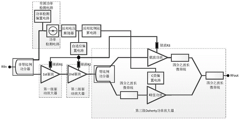
如图1所示,一种功率自适应Doherty功率放大器,其结构包括:非等比例功分器,有源功率检测电路(功率检测偏置电路、功率检测电路并联),反相电压跟随器,反相比例运算电路,自适应偏置电路,第一级驱动放大器(1st驱放),第二级驱动放大器(2nd驱放),第三级Doherty功率放大器(载波功放、峰值功放并联),等比例功分器,C类偏置电路,限流电阻R1、R2、R3,第一四分之波长微带线,第二四分之波长微带线,第三四分之波长微带线。As shown in Figure 1, a kind of power self-adaptive Doherty power amplifier, its structure comprises: non-equal ratio power splitter, active power detection circuit (power detection bias circuit, power detection circuit parallel connection), inverting voltage follower, Inverse proportional operation circuit, adaptive bias circuit, first-stage drive amplifier (1st drive amplifier), second-stage drive amplifier (2nd drive amplifier), third-stage Doherty power amplifier (carrier power amplifier, peak power amplifier in parallel), etc. Proportional power divider, class C bias circuit, current limiting resistors R1, R2, R3, first quarter-wavelength microstrip line, second quarter-wavelength microstrip line, third quarter-wavelength microstrip line.
非等比例功分器的一端为输入端,非等比例功分器的下输出端与第一级驱动放大器(1st驱放)输入端连接,上输出端与有源功率检测电路(功率检测偏置电路、功率检测电路并联)的一端连接;有源功率检测电路(功率检测偏置电路、功率检测电路并联)的另一端与反相电压跟随器的一端连接;反相电压跟随器的另一端分别与反相比例运算电路、自适应偏置电路的一端连接;自适应偏置电路的另一端分别与限流电阻R1、R2、R3的一端连接;反相比例运算电路的另一端与C类偏置电路的一端连接;第一级驱动放大器(1st驱放)的一端与限流电阻R1另一端连接,输出端与第二级驱动放大器(2nd驱放)的输入端连接;第二级驱动放大器(2nd驱放)的一端与限流电阻R2另一端连接,输出端与等比例功分器的输入端连接;等比例功分器的上输出端与载波功放输入端连接,下输出端与第一四分之波长微带线的一端连接;第一四分之波长微带线的另一端与峰值功放输入端连接;载波功放的一端与限流电阻R3的另一端连接,输出端与第二四分之波长微带线的一端连接;峰值功放的一端与C类偏置电路的另一端连接;第三四分之波长微带线的一端分别与峰值功放的输出端,第二四分之波长微带线的另一端连接;第三四分之波长微带线的另一端为输出端。One end of the non-equal ratio power divider is the input end, the lower output end of the non-equal ratio power splitter is connected to the input end of the first-stage drive amplifier (1st drive amplifier), and the upper output end is connected to the active power detection circuit (power detection bias The other end of the active power detection circuit (power detection bias circuit, power detection circuit in parallel) is connected to one end of the reverse voltage follower; the other end of the reverse voltage follower Connect to one end of the inverse proportional operation circuit and the adaptive bias circuit respectively; the other end of the adaptive bias circuit is respectively connected to one end of the current limiting resistors R1, R2, R3; the other end of the inverse proportional operation circuit is connected to the class C One end of the bias circuit is connected; one end of the first stage drive amplifier (1st drive amplifier) is connected to the other end of the current limiting resistor R1, and the output terminal is connected to the input end of the second stage drive amplifier (2nd drive amplifier); the second stage drive One end of the amplifier (2nd driving amplifier) is connected to the other end of the current limiting resistor R2, and the output end is connected to the input end of the proportional power divider; the upper output end of the equal proportional power divider is connected to the input end of the carrier power amplifier, and the lower output end is connected to the input end of the carrier amplifier. One end of the first quarter-wavelength microstrip line is connected; the other end of the first quarter-wavelength microstrip line is connected to the input end of the peak power amplifier; one end of the carrier power amplifier is connected to the other end of the current limiting resistor R3, and the output end is connected to the second end of the peak power amplifier. One end of the two-quarter wavelength microstrip line is connected; one end of the peak power amplifier is connected to the other end of the C bias circuit; one end of the third quarter-wavelength microstrip line is connected to the output end of the peak power amplifier, and the second quarter-wavelength The other end of the wavelength microstrip line is connected; the other end of the third quarter wavelength microstrip line is the output end.
在本实施例中,所述功率自适应Doherty功率放大器中,设计为三级功放级联架构,三级功放分别为:第一级驱动放大器(1st驱放)、第二级驱动放大器(2nd驱放)、第三级Doherty功率放大器(载波功放、峰值功放并联)。In this embodiment, the power adaptive Doherty power amplifier is designed as a three-stage power amplifier cascaded architecture, and the three-stage power amplifiers are: the first-stage drive amplifier (1st drive amplifier), the second-stage drive amplifier (2nd drive amplifier) Amplifier), third-stage Doherty power amplifier (carrier power amplifier, peak power amplifier in parallel).
该结构为大功率高线性度功率自适应Doherty功率放大器的典型结构,该典型架构可以根据功率容量需求设计为更小功率容量的单级Doherty功率放大器架构(无前两级驱动放大器)、两级功放级联架构(第一级驱动放大器级联Doherty功率放大器)以及设计为更大功率容量的多级功放级联架构(多级驱动放大器级联Doherty功率放大器),该设计为本发明提出的Doherty功率放大器结构提供了大功率设计的有效保障。This structure is a typical structure of a high-power high-linearity power adaptive Doherty power amplifier. This typical architecture can be designed as a single-stage Doherty power amplifier architecture with a smaller power capacity (without the first two-stage drive amplifier), and a two-stage power amplifier according to the power capacity requirements. Power amplifier cascaded architecture (the first-stage drive amplifier cascaded Doherty power amplifier) and the multistage power amplifier cascaded architecture (multi-stage drive amplifier cascaded Doherty power amplifier) designed as larger power capacity, this design is the Doherty power amplifier proposed by the present invention The power amplifier structure provides an effective guarantee for high-power design.
如图2所示,在本实施例中,所述有源功率检测电路由功率检测偏置电路和功率检测电路并联组成,具体包括:电容C3,二极管D1,第一滤波电容C2,负载电阻R7,镇流电阻R6,第一镜像电流源HBT1、HBT2、HBT3,第一电阻R5,第一电容C1,第一电源Vcc。As shown in Figure 2, in this embodiment, the active power detection circuit is composed of a power detection bias circuit and a power detection circuit connected in parallel, specifically including: a capacitor C3, a diode D1, a first filter capacitor C2, and a load resistor R7 , a ballast resistor R6, a first mirror current source HBT1, HBT2, HBT3, a first resistor R5, a first capacitor C1, and a first power supply Vcc.
电容C3一端为输入端,电容C3输出端分别与镇流电阻R6、二极管D1的一端连接;二极管D1的另一端分别与第一滤波电容C2、负载电阻R7的一端连接;第一滤波电容C2与负载电阻R7并联,另一端接地;负载电阻R7另一端接地;第一电源Vcc分别与第一电阻R5的一端,第一镜像电流源HBT1集电极连接;第一电阻R5的另一端分别与第一镜像电流源HBT1、HBT2的基极,第一镜像电流源HBT2的集电极,第一电容C1的一端连接;第一镜像电流源HBT1的发射极与镇流电阻R6的另一端连接;第一电容C1的另一端接地;第一镜像电流源HBT2的发射极分别与第一镜像电流源HBT3的基极和集电极连接;镜像电流源HBT3的发射极接地。One end of the capacitor C3 is the input end, and the output end of the capacitor C3 is respectively connected to the ballast resistor R6 and one end of the diode D1; the other end of the diode D1 is respectively connected to the first filter capacitor C2 and one end of the load resistor R7; the first filter capacitor C2 is connected to The load resistor R7 is connected in parallel, and the other end is grounded; the other end of the load resistor R7 is grounded; the first power supply Vcc is respectively connected to one end of the first resistor R5 and the collector of the first mirror current source HBT1; the other end of the first resistor R5 is respectively connected to the first The bases of the mirror current sources HBT1 and HBT2, the collector of the first mirror current source HBT2, and one end of the first capacitor C1 are connected; the emitter of the first mirror current source HBT1 is connected to the other end of the ballast resistor R6; the first capacitor The other end of C1 is grounded; the emitter of the first mirror current source HBT2 is respectively connected to the base and collector of the first mirror current source HBT3; the emitter of the mirror current source HBT3 is grounded.
如图3所示,在本实施例中,进一步地,所述反相电压跟随器中,具体包括:第一补偿电阻R3,调控电阻R1、R2、R4、R5、R6、R7,第一反相放大器,第一加法器。As shown in Figure 3, in this embodiment, further, the reverse phase voltage follower specifically includes: a first compensation resistor R3, regulation resistors R1, R2, R4, R5, R6, R7, a first reverse phase phase amplifier, first adder.
调控电阻R1一端为输入端,调控电阻R1的输出端分别与第一反相放大器反向输入端,调控电阻R2的一端连接;第一补偿电阻R3一端与第一反相放大器同向输入端连接,另一端接地;调控电阻R2另一端与第一反相放大器输出端共同连接调控电阻R4的一端;调控电阻R6的一端为输入端,调控电阻R6的输出端与调控电阻R4的另一端共同连接第一加法器的同向输入端;调控电阻R5的一端分别与第一加法器的反向输入端,调控电阻R7的一端连接,另一端接地;调控电阻R7的另一端与第一加法器的输出端连接。One end of the control resistor R1 is the input terminal, and the output terminal of the control resistor R1 is respectively connected to the inverting input terminal of the first inverting amplifier and one end of the control resistor R2; one end of the first compensation resistor R3 is connected to the same input terminal of the first inverting amplifier , the other end is grounded; the other end of the control resistor R2 is connected to the output terminal of the first inverting amplifier; The same direction input end of the first adder; one end of the regulating resistor R5 is respectively connected with the reverse input end of the first adding device, one end of the regulating resistor R7 is connected, and the other end is grounded; the other end of the regulating resistor R7 is connected with the first adding device output connection.
如图4所示,在本实施例中,所述自适应偏置电路中,基于镜像电流源结构实现一个共用型自适应偏置电路,具体包括:第一电阻R0,第一电阻R4,第二镜像电流源HBT1、HBT2、HBT3,第二滤波电容C2,第二电容C1,第二电源Vcc。As shown in FIG. 4, in the present embodiment, in the adaptive bias circuit, a common adaptive bias circuit is implemented based on the mirror current source structure, which specifically includes: a first resistor R0, a first resistor R4, a first Two mirror current sources HBT1, HBT2, HBT3, a second filter capacitor C2, a second capacitor C1, and a second power supply Vcc.
第二电源Vcc与第二镜像电流源HBT1集电极连接;第二镜像电流源HBT1发射极分别与第一电阻R0,第二滤波电容C2一端连接;第一电阻R0和第二滤波电容C2并联,另一端分别与上述限流电阻R1、R2、R3一端连接;第一电阻R4一端为输入端,第一电阻R4的输出端分别与第二镜像电流源HBT2集电极、基极,第二镜像电流源HBT1基极,第二电容C1的一端连接;第二电容C1另一端接地;第二镜像电流源HBT2发射极分别与第二镜像电流源HBT3集电极,基极连接;第二镜像电流源HBT3发射极接地。The second power supply Vcc is connected to the collector of the second mirror current source HBT1; the emitter of the second mirror current source HBT1 is respectively connected to the first resistor R0 and one end of the second filter capacitor C2; the first resistor R0 and the second filter capacitor C2 are connected in parallel, The other ends are respectively connected to one end of the above-mentioned current-limiting resistors R1, R2, and R3; one end of the first resistor R4 is an input end, and the output end of the first resistor R4 is respectively connected to the collector and base of the second mirror current source HBT2, and the second mirror current The source HBT1 base is connected to one end of the second capacitor C1; the other end of the second capacitor C1 is grounded; the emitter of the second mirror current source HBT2 is respectively connected to the collector and base of the second mirror current source HBT3; the second mirror current source HBT3 The emitter is grounded.
如图5所示,在本实施例中,所述反相比例运算电路中,具体包括:第一电阻R1、R2,第二补偿电阻R3,第二反相放大器。As shown in FIG. 5 , in this embodiment, the inverse proportional operation circuit specifically includes: first resistors R1 and R2 , a second compensation resistor R3 , and a second inverting amplifier.
第一电阻R1一端为输入端,第一电阻R1的输出端分别与第一电阻R2一端,第二反相放大器反向输入端连接;第二补偿电阻R3一端与第二反相放大器同向输入端连接,另一端接地;第二反相放大器输出端与第一电阻R2另一端连接。One end of the first resistor R1 is the input end, and the output end of the first resistor R1 is respectively connected to one end of the first resistor R2 and the inverting input end of the second inverting amplifier; one end of the second compensation resistor R3 is input in the same direction as the second inverting amplifier connected to one end and the other end to ground; the output end of the second inverting amplifier is connected to the other end of the first resistor R2.
如图6所示,在本实施例中,所述C类偏置电路中,具体包括:可控电压源S1,电感RF_choc,第二电阻R1、R2,第三电容C1。As shown in FIG. 6 , in this embodiment, the class C bias circuit specifically includes: a controllable voltage source S1 , an inductor RF_choc, second resistors R1 and R2 , and a third capacitor C1 .
输入端与可控电压源S1相连,可控电压源S1正极为输出端,可控电压源S1的负极接地;电感RF_choc输入端与可控电压源S1输出端连接,电感RF_choc输出端与第二电阻R1一端连接;第二电阻R1另一端分别与第二电阻R2,第三电容C1一端连接;第二电阻R2和第三电容C1并联,另一端接地。The input end is connected to the controllable voltage source S1, the positive pole of the controllable voltage source S1 is the output end, and the negative pole of the controllable voltage source S1 is grounded; the input end of the inductor RF_choc is connected to the output end of the controllable voltage source S1, and the output end of the inductor RF_choc is connected to the second One end of the resistor R1 is connected; the other end of the second resistor R1 is respectively connected with the second resistor R2 and one end of the third capacitor C1; the second resistor R2 is connected in parallel with the third capacitor C1, and the other end is grounded.
如图7所示,本发明还提出了一种功率自适应Doherty功率放大器设计方法,具体步骤如下:As shown in Figure 7, the present invention also proposes a method for designing a power adaptive Doherty power amplifier, and the specific steps are as follows:
S1、获得放大器设计目标,明确:增益、输出功率、效率等指标;S1. Obtain the design goals of the amplifier, and clarify: gain, output power, efficiency and other indicators;
S2、根据增益、功率容量等选定三极管类型;S2. Select the transistor type according to the gain, power capacity, etc.;
S3、确认是否需要驱动级放大器,若需要,先确定驱动级放大器级数后,再确定每一级放大器三极管数量(包括载波功放和峰值功放),若不需要,则直接确定每一级放大器三极管数量;S3. Confirm whether the driver stage amplifier is needed. If necessary, first determine the number of stages of the driver stage amplifier, and then determine the number of amplifier transistors in each stage (including carrier power amplifier and peak power amplifier). If not, directly determine the amplifier transistors in each stage quantity;
S4、基于步骤S3,明确输入功率范围,找到输入功率中间点;S4. Based on step S3, specify the input power range, and find the middle point of the input power;
S5、根据找到输入功率中间点确定各级放大器的偏置点,从而确定限流电阻R1、R2、R3的参数以及确定自适应偏置电路模块中各元器件参数;S5. Determine the bias points of the amplifiers at all levels according to finding the middle point of the input power, thereby determining the parameters of the current limiting resistors R1, R2, R3 and determining the parameters of each component in the adaptive bias circuit module;
S6、确定C类偏置电路模块中各元器件参数;S6. Determine the parameters of each component in the C-type bias circuit module;
S7、确定等比例功分器、四分之波长微带线参数,获得不含功率自适应功能的Doherty功放基本功能和性能;S7. Determine the parameters of the equal ratio power divider and the quarter-wavelength microstrip line, and obtain the basic functions and performance of the Doherty power amplifier without power adaptive function;
S8、根据不含功率自适应功能的Doherty功放基本性能确定非等比例功分器参数(最重要为确定分配比例);S8. Determine the parameters of the non-equal power splitter according to the basic performance of the Doherty power amplifier without the power adaptive function (the most important thing is to determine the distribution ratio);
S9、根据不含功率自适应功能的Doherty功放基本性能确定功率检测偏置电路模块的元器件参数,确定功率检测电路的偏置电压,确定功率检测电路模块的元器件参数,确定负载电阻参数;S9. Determine the component parameters of the power detection bias circuit module according to the basic performance of the Doherty power amplifier without power adaptive function, determine the bias voltage of the power detection circuit, determine the component parameters of the power detection circuit module, and determine the load resistance parameter;
S10、根据自适应偏置电路模块以及C类偏置电路模块参数确定反相电压跟随器模块电路以及反相比例运算电路模块各元器件参数;S10. Determine the parameters of each component of the inverse voltage follower module circuit and the inverse proportional operation circuit module according to the parameters of the adaptive bias circuit module and the C-type bias circuit module;
S11、采用全输入功率范围运行整个Doherty功放以验证是否满足功率自适应要求,若不满足,重复步骤S7-S10直到满足,设计结束。S11. Run the entire Doherty power amplifier with the full input power range to verify whether the power self-adaptive requirement is met. If not, repeat steps S7-S10 until it is met, and the design ends.
在本实施例中,所述功率自适应Doherty功率放大器中,具体流程如下:In this embodiment, in the power adaptive Doherty power amplifier, the specific process is as follows:
射频信号从Rfin端口进入功放,首先到达非等比例功分器的输入端口,该功分器按照有源功率检测电路的灵敏度划分功率比,如RFin端口进入的输入功率的百分之一即可使得功率检测电路工作,即将非等比例功分器的功率分配比例定为1:100予以设计。射频信号经过非等比例功分器一分为二,一部分信号通过主路进入第一级驱动放大器(1st驱放),经过放大后,再进入第二级驱动放大器(2nd驱放);这两级功率放大器按照需求被自适应偏置电路模块偏置在A类和AB类,最大程度保障信号的线性度,避免放大器过早增益压缩。信号经过第二级驱动放大器(2nd驱放)放大后,到达Doherty功率放大器(载波功放、峰值功放并联)输入端口,即等比例功分器的输入端口;信号经过等比例功分器后,等比例一分为二,进入Doherty功率放大器的载波功放和峰值功放;载波功放后有一段四分之一波长微带线,为保证相位相同,峰值功放前也接有一段四分之一波长微带线;载波功放一般工作在AB类,峰值功放一般工作在C类;当输入信号较小时,由于峰值功放工作在C类,处于截断状态,只有载波功放参与放大;加之四分之一波长微带线的作用,载波功放看到的负载为高阻抗,使得功率功放工作在高效率状态;当输入信号增大至峰值功放开启时,由于峰值功放有信号经过使得载波功放看到的负载为低阻抗,保障高效率的同时Doherty功放整体输出功率增大,Doherty功率放大器合路输出端口的四分之一波长微带线的作用是将合路的阻抗变换至50欧姆。The radio frequency signal enters the power amplifier from the Rfin port, and first reaches the input port of the non-equal power splitter. The power splitter divides the power ratio according to the sensitivity of the active power detection circuit, such as one percent of the input power entering the RFin port. To make the power detection circuit work, that is to design the power distribution ratio of the non-equal power divider as 1:100. The RF signal is divided into two by a non-equal power divider, and part of the signal enters the first-stage drive amplifier (1st drive amplifier) through the main circuit, and then enters the second-stage drive amplifier (2nd drive amplifier) after being amplified; The first-class power amplifier is biased in class A and class AB by the adaptive bias circuit module according to the requirements, which guarantees the linearity of the signal to the greatest extent and avoids premature gain compression of the amplifier. After the signal is amplified by the second-stage drive amplifier (2nd drive amplifier), it reaches the input port of the Doherty power amplifier (carrier power amplifier, peak power amplifier in parallel), that is, the input port of the proportional power divider; after the signal passes through the equal proportion power divider, etc. The ratio is divided into two, entering the carrier power amplifier and peak power amplifier of the Doherty power amplifier; there is a quarter-wavelength microstrip line after the carrier power amplifier, and a quarter-wavelength microstrip line is also connected before the peak power amplifier to ensure the same phase line; the carrier power amplifier generally works in class AB, and the peak power amplifier generally works in class C; when the input signal is small, because the peak power amplifier works in class C, it is in a truncated state, and only the carrier power amplifier participates in amplification; The effect of the line, the load seen by the carrier power amplifier is high impedance, so that the power power amplifier works in a high-efficiency state; when the input signal increases to the peak power amplifier, the load seen by the carrier power amplifier is low impedance due to the signal passing through the peak power amplifier , while ensuring high efficiency, the overall output power of the Doherty power amplifier is increased. The function of the quarter-wavelength microstrip line at the combined output port of the Doherty power amplifier is to transform the combined impedance to 50 ohms.
以上的主路信号实现高功率和高效率的放大,经过非等比例功分器一分为二的另一部分的信号通过支路进入有源功率检测电路,有源功率检测电路输出的直流信号再被送达至反相电压跟随器,随后该反相电压跟随器输出信号被分为两路加以处理,第一路反相电压跟随器输出信号送入自适应偏置电路中,用于调控自适应偏置电路给第一级驱动放大器(1st驱放)、第二级驱动放大器(2nd驱放)以及Doherty功率放大器的载波功放的偏置电流,实现第一级驱动放大器(1st驱放)、第二级驱动放大器(2nd驱放)以及Doherty功率放大器的载波功放的偏置点和增益随着整个放大器输入功率的变化而被动态调控;第二路反相电压跟随器输出信号被送入反相比例运算电路中;该信号通过反相比例运算电路输出后,传送至C类偏置电路,用于调控C类偏置电路给Doherty功率放大器的峰值功放的偏置电流,实现了Doherty功率放大器的峰值功放的偏置点和增益随着整个放大器输入功率的变化而被动态调控,综上实现了整个功率放大器的功率自适应。The above main signal can be amplified with high power and high efficiency, and the other part of the signal which is divided into two by the non-equal power divider enters the active power detection circuit through the branch circuit, and the DC signal output by the active power detection circuit is regenerated. is sent to the inverting voltage follower, and then the output signal of the inverting voltage follower is divided into two channels for processing, and the output signal of the first inverting voltage follower is sent to the adaptive bias circuit for regulating the self Adapt to the bias current of the bias circuit to the first-stage drive amplifier (1st drive amplifier), the second-stage drive amplifier (2nd drive amplifier) and the carrier power amplifier of the Doherty power amplifier to realize the first-stage drive amplifier (1st drive amplifier), The bias point and gain of the carrier power amplifier of the second-stage drive amplifier (2nd drive amplifier) and the Doherty power amplifier are dynamically adjusted as the input power of the entire amplifier changes; the output signal of the second inverting voltage follower is sent to the inverting In the phase proportional operation circuit; after the signal is output by the inverse proportional operation circuit, it is sent to the C-class bias circuit, which is used to regulate the bias current of the C-class bias circuit to the peak power amplifier of the Doherty power amplifier, and realizes the Doherty power amplifier The bias point and gain of the peak power amplifier are dynamically regulated as the input power of the whole amplifier changes, and the power self-adaptation of the whole power amplifier is realized in summary.
在本实施例中,所述有源功率检测电路中,具体如下:In this embodiment, in the active power detection circuit, the details are as follows:
到达有源检测电路模块的信号首先到达功率检测电路的Rfin端口,该功率检测电路模块是串联二极管型整流电路,射频信号经过二极管D1和第一滤波电容C2被转化为直流电压信号加载在负载电阻R7上,因此负载电阻R7上的电压信号幅值Vpdect可以反映输入功率Rfin的大小;该功率检测电路模块中负载电阻R7的选择与功率检测偏置电路模块可以决定整个有源功率检测电路模块的灵敏度与分辨率。The signal reaching the active detection circuit module first reaches the Rfin port of the power detection circuit. The power detection circuit module is a series diode rectifier circuit. The radio frequency signal is converted into a DC voltage signal through the diode D1 and the first filter capacitor C2 and loaded on the load resistor. On R7, the voltage signal amplitude Vpdect on the load resistor R7 can reflect the size of the input power Rfin; the selection of the load resistor R7 in the power detection circuit module and the power detection bias circuit module can determine the entire active power detection circuit module. Sensitivity and resolution.
功率检测偏置电路基于镜像电流源实现,该偏置电路由第一镜像电流源HBT1、HBT2、HBT3构成,再由镇流电阻R6为二极管D1提供直流偏置,可以改善射频信号泄露进入偏置电路端口的阻抗。功率检测偏置电路有两个功能,第一为功率检测电路提供直流偏置,第二为功率检测电路实现温度不敏感特性和线性化改善:The power detection bias circuit is implemented based on the mirror current source. The bias circuit is composed of the first mirror current source HBT1, HBT2, and HBT3, and the ballast resistor R6 provides a DC bias for the diode D1, which can improve the RF signal leakage into the bias The impedance of a circuit port. The power detection bias circuit has two functions. The first is to provide a DC bias for the power detection circuit, and the second is to achieve temperature insensitivity and linearization improvement for the power detection circuit:
第一功能的工作流程为:来自于第一电源Vcc的电流,经过第一电阻R5和第一镜像电流源HBT1、HBT2、HBT3,实现对第一镜像电流源HBT1集电极电流的控制,因此来自于第一电源Vcc且受控的电流从第一镜像电流源HBT1集电极流向第一镜像电流源HBT1发射极,经过镇流电阻R6提供给整流二极管D1,从而使得整流二极管处于导通状态,在输入信号足够微弱时也可以工作并有输出,同时保障功率检测电路的输出初始值为一个适合后续电路的电压值;The working process of the first function is: the current from the first power supply Vcc passes through the first resistor R5 and the first mirror current sources HBT1, HBT2, and HBT3 to realize the control of the collector current of the first mirror current source HBT1, so from The current controlled by the first power supply Vcc flows from the collector of the first mirror current source HBT1 to the emitter of the first mirror current source HBT1, and is supplied to the rectifier diode D1 through the ballast resistor R6, so that the rectifier diode is in a conduction state. When the input signal is weak enough, it can also work and have an output, and at the same time ensure that the initial value of the output of the power detection circuit is a voltage value suitable for the subsequent circuit;
第二功能的工作流程为:进入Rfin端口的射频信号经过电容C3分为两路,第一路为主路,绝大部分(一般设定为二十分之十九,由镇流电阻R6的阻值确定)的射频信号经过整流二极管D1,以及第一滤波电容C2最后变成直流信号加载在负载电阻R7上,因此负载电阻R7上的电压信号幅值Vpdect可以反映输入功率Rfin的大小。小部分(一般设定为二十分之一,由镇流电阻R6的阻值确定)的射频信号经过镇流电阻R6进入镜像电流源,经过第一镜像电流源HBT1的基极-发射极二极管,最后通过第一电容C1旁路到地,由于第一镜像电流源HBT1的基极-发射极二极管的钳位效应,在进入Rfin端口的射频信号功率变大或者环境温度升高的情况下,第一镜像电流源HBT1的基极-发射极电压的变化可以补偿整流二极管D1的阈值电压点的漂移,从而实现功率检测电路温度不敏感特性和线性化改善功能。The working process of the second function is: the radio frequency signal entering the Rfin port is divided into two paths through the capacitor C3, the first path is the main path, most of them (generally set to 19 out of 20, and are controlled by the ballast resistor R6) The radio frequency signal whose resistance value is determined) passes through the rectifier diode D1, and the first filter capacitor C2 finally becomes a DC signal loaded on the load resistor R7, so the voltage signal amplitude Vpdect on the load resistor R7 can reflect the size of the input power Rfin. A small part (generally set to one-twentieth, determined by the resistance of the ballast resistor R6) RF signal enters the mirror current source through the ballast resistor R6, and passes through the base-emitter diode of the first mirror current source HBT1 , and finally bypassed to the ground through the first capacitor C1, due to the clamping effect of the base-emitter diode of the first mirror current source HBT1, when the power of the radio frequency signal entering the Rfin port becomes larger or the ambient temperature rises, The change of the base-emitter voltage of the first mirror current source HBT1 can compensate the drift of the threshold voltage point of the rectifier diode D1, so as to realize the temperature insensitivity characteristic of the power detection circuit and the linearization improvement function.
第一镜像电流源HBT1的基极-发射极电压在整个Doherty功放高输入功率下和温度变化时的变化(基极-发射极二极管钳位效应)可以补偿二极管本身的电压变化,第一电容C1的作用使得泄露进偏置电路的射频信号旁路到地,从而稳定B点电压,从而使得整个有源功率检测电路具有了功率稳定性和温度不敏感特性,保障了有源功率检测电路的可靠性。同时,功率检测偏置电路为功率检测电路的输出电压信号幅值Vpdect提供了起始电压,即功率检测电路的输出电压信号幅值Vpdect可以不是从0V开始变化,而是从设定某个电压值开始变化,如2.5V等。The change of the base-emitter voltage of the first mirror current source HBT1 under the high input power of the whole Doherty power amplifier and the change of temperature (base-emitter diode clamping effect) can compensate the voltage change of the diode itself, and the first capacitor C1 The role of the RF signal that leaks into the bias circuit is bypassed to the ground, thereby stabilizing the voltage at point B, so that the entire active power detection circuit has power stability and temperature insensitivity characteristics, ensuring the reliability of the active power detection circuit sex. At the same time, the power detection bias circuit provides an initial voltage for the output voltage signal amplitude Vpdect of the power detection circuit, that is, the output voltage signal amplitude Vpdect of the power detection circuit may not change from 0V, but from a certain voltage The value starts changing like 2.5V etc.
在本实施例中,所述反相电压跟随器中,反应整个Doherty功放输入功率的电压信号Vpdect会被加以处理和利用,该信号被送达至反相电压跟随器,具体如下:In this embodiment, in the inverting voltage follower, the voltage signal Vpdect reflecting the input power of the entire Doherty power amplifier will be processed and utilized, and the signal will be sent to the inverting voltage follower, as follows:
该反相电压跟随模块由反相放大电路和加法器电路级联实现,该电路中的电压Vmid为反相放大电路输出电压,其计算公式为:The inverting voltage follower module is implemented by cascading an inverting amplifier circuit and an adder circuit. The voltage Vmid in this circuit is the output voltage of the inverting amplifier circuit, and its calculation formula is:

该电路中,第一补偿电阻R3保证运放输入差分放大电路外接电阻的对称性,如果:In this circuit, the first compensation resistor R3 ensures the symmetry of the external resistance of the operational amplifier input differential amplifier circuit, if:
R2=R1R2=R1
则有:Then there are:
Vmid=-VpdectVmid=-Vpdect
中点电压Vmid与输入电压大小相当,方向反相,则下一级加法器电路同(正)向输入V+为:The midpoint voltage Vmid is equal to the input voltage, and the direction is reversed, so the next-stage adder circuit has the same (positive) input V + as:

其中,Vref表示参考电压。Wherein, Vref represents a reference voltage.
进一步可计算出:It can be further calculated:

则可以实现对输入电压Vpdect的反相跟随,如当输入动态电压为1V至3V,则反相电压跟随器模块的输出电压为3V至1V。Then the reverse phase follower of the input voltage Vpdect can be realized. For example, when the input dynamic voltage is 1V to 3V, the output voltage of the reverse phase voltage follower module is 3V to 1V.
其中,反相电压跟随器模块的输出电压命名为Vbctrl,该电压会被分为两路加以利用或处理。Wherein, the output voltage of the inverting voltage follower module is named Vbctrl, and the voltage will be divided into two channels for utilization or processing.
本实施例中,所述自适应偏置电路中,具体如下:In this embodiment, in the adaptive bias circuit, the details are as follows:
不同于传统功率放大器需要给各级功放设计独立偏置电路,本实施例中,基于镜像电流源结构实现一个共用型自适应偏置电路,镜像电流源基本结构由第二镜像电流源HBT1、HBT2、HBT3构成,再由三枚镇流电阻R1、R2和R3分别为一级驱动放大器(1st驱放)、第二级驱动放大器(2nd驱放)、Doherty功率放大器的载波功放提供基极偏置电流,三枚镇流电阻R1、R2和R3不同的阻值以及第一电阻R0、R4共同实现了不同的偏置电流,从而为第一级驱动放大器(1st驱放)、第二级驱动放大器(2nd驱放)、Doherty功率放大器的载波功放提供不同的偏置点。Unlike traditional power amplifiers, which need to design independent bias circuits for power amplifiers at all levels, in this embodiment, a common adaptive bias circuit is implemented based on the mirror current source structure. The basic structure of the mirror current source is composed of the second mirror current source HBT1, HBT2 , HBT3, and then three ballast resistors R1, R2 and R3 respectively provide base bias for the first-stage drive amplifier (1st drive amplifier), the second-stage drive amplifier (2nd drive amplifier), and the carrier power amplifier of the Doherty power amplifier Current, the different resistance values of the three ballast resistors R1, R2 and R3 and the first resistors R0 and R4 together achieve different bias currents, thus providing the first stage drive amplifier (1st drive amplifier), the second stage drive amplifier (2nd drive amplifier), Doherty power amplifier carrier power amplifier provides different bias points.
一般情况下,第一级驱动放大器(1st驱放)和第二级驱动放大器(2nd驱放)偏置在A类,载波功放偏置在AB类。偏置电路中第一电阻R0与第二滤波电容C2可以改善射频信号泄露进入偏置电路端口的阻抗,特别是第二滤波电容C2的设计,可以有效改善偏置电路的宽带特性。第二镜像电流源HBT1的基极-发射极电压在功放高输入功率以及温度变化情况下的变化(基极-发射极二极管钳位效应)可以补偿一级驱动放大器(1st驱放)、第二级驱动放大器(2nd驱放)、Doherty功率放大器的载波功放在高输入功率以及温度变化情况下的基极-发射极电压变化,第二电容C1的作用使得泄露进偏置电路的射频信号旁路到地,从而稳定B点电压。基于以上设计使得该共用型自适应偏置电路具有良好的温度不敏感自适应线性化改善特性。为本发明提出的Doherty功率放大器提供了高线性度的有效保障。In general, the first stage driver amplifier (1st drive amplifier) and the second stage drive amplifier (2nd drive amplifier) are biased in class A, and the carrier power amplifier is biased in class AB. The first resistor R0 and the second filter capacitor C2 in the bias circuit can improve the impedance of the RF signal leaking into the port of the bias circuit, especially the design of the second filter capacitor C2 can effectively improve the broadband characteristics of the bias circuit. The change of the base-emitter voltage of the second mirror current source HBT1 in the case of high input power of the power amplifier and temperature change (base-emitter diode clamping effect) can compensate the first-stage drive amplifier (1st drive amplifier), the second Stage drive amplifier (2nd drive amplifier), base-emitter voltage change of the carrier power amplifier of Doherty power amplifier under high input power and temperature change, the role of the second capacitor C1 bypasses the RF signal leaked into the bias circuit to ground to stabilize the voltage at point B. Based on the above design, the common adaptive bias circuit has good temperature-insensitive adaptive linearization improvement characteristics. An effective guarantee of high linearity is provided for the Doherty power amplifier proposed by the present invention.
上述反相电压跟随器模块的输出电压中第一路Vbctrl信号被送入自适应偏置电路模块中的第一电阻R4一端,自适应偏置电路有两个功能,第一为第一级驱动放大器(1st驱放)、第二级驱动放大器(2nd驱放)、Doherty功率放大器的载波功放提供直流偏置,第二为第一级驱动放大器(1st驱放)、第二级驱动放大器(2nd驱放)、Doherty功率放大器的载波功放实现温度不敏感特性和线性化改善:The first Vbctrl signal in the output voltage of the above-mentioned inverting voltage follower module is sent to the end of the first resistor R4 in the adaptive bias circuit module. The adaptive bias circuit has two functions, the first is the first-level drive Amplifier (1st driver amplifier), second driver amplifier (2nd driver amplifier), carrier power amplifier of Doherty power amplifier provides DC bias, the second is the first driver amplifier (1st driver amplifier), second driver amplifier (2nd driver amplifier) drive amplifier), Doherty power amplifier carrier power amplifier to achieve temperature insensitivity and linearity improvement:
第一功能的工作流程为:来自于第二电源Vcc的电流,经过第一电阻R4和第二镜像电流源HBT1、HBT2、HBT3,实现对第二镜像电流源HBT1集电极电流的控制,因此来自于第二电源Vcc且受控的电流从第二镜像电流源HBT1集电极流向第二镜像电流源HBT1发射极,经过第一电阻R0,限流电阻R1、R2、R3提供给第一级驱动放大器(1st驱放)、第二级驱动放大器(2nd驱放)、Doherty功率放大器的载波功放,从而使得第一级驱动放大器(1st驱放)、第二级驱动放大器(2nd驱放)、Doherty功率放大器的载波功放偏置在合适的偏置类型(A类和AB类);The working process of the first function is: the current from the second power supply Vcc passes through the first resistor R4 and the second mirror current source HBT1, HBT2, HBT3 to realize the control of the collector current of the second mirror current source HBT1, so from The current controlled by the second power supply Vcc flows from the collector of the second mirror current source HBT1 to the emitter of the second mirror current source HBT1, passes through the first resistor R0, and the current limiting resistors R1, R2, and R3 are supplied to the first-stage drive amplifier (1st drive amplifier), second stage drive amplifier (2nd drive amplifier), carrier power amplifier of Doherty power amplifier, so that the first stage drive amplifier (1st drive amplifier), second stage drive amplifier (2nd drive amplifier), Doherty power amplifier The amplifier's carrier power amplifier is biased at the appropriate bias type (Class A and Class AB);
第二功能的工作流程为:进入第一级驱动放大器(1st驱放)、第二级驱动放大器(2nd驱放)、Doherty功率放大器的载波功放的射频信号会被分为两路,第一路为主路,绝大部分(一般设定为二十分之十九,由第一电阻R0,限流电阻R1、R2、R3的阻值以及第二滤波电容C2的容值确定)的射频信号经过第一级驱动放大器(1st驱放)、第二级驱动放大器(2nd驱放)、Doherty功率放大器的载波功放放大至后级电路。小部分(一般设定为二十分之一,由第一电阻R0,限流电阻R1、R2、R3的阻值以及第二滤波电容C2的容值确定)的射频信号经过第一电阻R0,限流电阻R1、R2、R3以及第二滤波电容C2进入镜像电流源,经过第二镜像电流源HBT1的基极-发射极二极管,最后通过第二电容C1旁路到地,由于第二镜像电流源HBT1的基极-发射极二极管的钳位效应,在进入第一级驱动放大器(1st驱放)、第二级驱动放大器(2nd驱放)、Doherty功率放大器的载波功放的射频信号功率变大或者环境温度升高的情况下,第二镜像电流源HBT1的基极-发射极电压的变化可以补偿第一级驱动放大器(1st驱放)、第二级驱动放大器(2nd驱放)、Doherty功率放大器的载波功放中各HBT管芯的基极-发射极电压的漂移,从而实现第一级驱动放大器(1st驱放)、第二级驱动放大器(2nd驱放)、Doherty功率放大器的载波功放的温度不敏感特性和线性化改善功能。The working process of the second function is: the RF signal entering the first-stage drive amplifier (1st drive amplifier), the second-stage drive amplifier (2nd drive amplifier), and the carrier power amplifier of the Doherty power amplifier will be divided into two channels. The main road, most of the radio frequency signal (generally set to 19/20, determined by the resistance of the first resistor R0, the resistance of the current limiting resistors R1, R2, R3 and the capacitance of the second filter capacitor C2) After the first-stage drive amplifier (1st drive amplifier), the second-stage drive amplifier (2nd drive amplifier), and the carrier power amplifier of the Doherty power amplifier, it is amplified to the subsequent stage circuit. A small part (generally set to one-twentieth, determined by the first resistor R0, the resistance values of the current limiting resistors R1, R2, R3 and the capacitance of the second filter capacitor C2) passes through the first resistor R0, The current limiting resistors R1, R2, R3 and the second filter capacitor C2 enter the mirror current source, pass through the base-emitter diode of the second mirror current source HBT1, and finally bypass the ground through the second capacitor C1, because the second mirror current The clamping effect of the base-emitter diode of the source HBT1 increases the power of the RF signal entering the first-stage drive amplifier (1st drive amplifier), the second-stage drive amplifier (2nd drive amplifier), and the carrier power amplifier of the Doherty power amplifier Or when the ambient temperature rises, the change of the base-emitter voltage of the second mirror current source HBT1 can compensate the first-stage drive amplifier (1st drive), the second-stage drive amplifier (2nd drive), Doherty power The drift of the base-emitter voltage of each HBT die in the carrier power amplifier of the amplifier, so as to realize the carrier power amplifier of the first stage drive amplifier (1st drive amplifier), the second stage drive amplifier (2nd drive amplifier), and the Doherty power amplifier Temperature insensitivity and linearization improvements.
Vbctrl信号幅值会随着输入功率的增大而线性变小,从而同步改变自适应偏置电路的控制电压,达到实时调控第一级驱动放大器(1st驱放)、第二级驱动放大器(2nd驱放)、Doherty功率放大器的载波功放偏置点和增益的目的,避免在过高的输入功率下功率放大器的饱和,或者说避免放大器饱和过早出现,反之亦然,当输入功率过低,Vbctrl信号幅值会随着输入功率的减小而线性增大,从而实时调控增大第一级驱动放大器(1st驱放)、第二级驱动放大器(2nd驱放)、Doherty功率放大器的载波功放增益的目的。为本实施例提出的Doherty功率放大器结构提供了功率自适应特性的有效保障。The amplitude of the Vbctrl signal will decrease linearly with the increase of the input power, thereby synchronously changing the control voltage of the adaptive bias circuit to achieve real-time regulation of the first-stage drive amplifier (1st drive amplifier) and the second-stage drive amplifier (2nd drive amplifier). Drive amplifier), Doherty power amplifier carrier power amplifier bias point and gain purpose, to avoid the saturation of the power amplifier under too high input power, or to avoid premature amplifier saturation, and vice versa, when the input power is too low, The amplitude of the Vbctrl signal will increase linearly with the decrease of the input power, so as to increase the carrier power amplifier of the first-stage drive amplifier (1st drive amplifier), the second-stage drive amplifier (2nd drive amplifier), and the Doherty power amplifier in real time. purpose of gain. The structure of the Doherty power amplifier proposed in this embodiment provides an effective guarantee for the power adaptive characteristic.
在本实施例中,所述反相比例运算电路中,具体如下:In this embodiment, in the inverse proportional operation circuit, the details are as follows:
上述反相电压跟随器模块的输出电压中第二路Vbctrl信号被送入反比例运算电路模块,该电路中第二补偿电阻R3保证运放输入差分放大电路外接电阻的对称性,如果:The second Vbctrl signal in the output voltage of the above-mentioned inverting voltage follower module is sent to the inverse proportional operation circuit module, and the second compensation resistor R3 in this circuit ensures the symmetry of the external resistance of the operational amplifier input differential amplifier circuit, if:
R2=R1R2=R1
则有:Then there are:
Vbias_c=-VbctrlVbias_c=-Vbctrl
即将第二路Vbctrl信号反相,如Vbctrl信号随着输入功率的变化呈3V至1V的变化,则Vbias_c信号的变化为-3V至-1V。That is, the second Vbctrl signal is reversed. If the Vbctrl signal changes from 3V to 1V with the input power, the Vbias_c signal changes from -3V to -1V.
在本实施例中,所述C类偏置电路中,反比例运算电路模块的输出信号为Vbias_c,该信号被送至C类偏置电路模块,具体如下:In this embodiment, in the class C bias circuit, the output signal of the inverse proportional operation circuit module is Vbias_c, and this signal is sent to the class C bias circuit module, specifically as follows:
反比例运算电路模块的输出信号Vbias_c被传送至可控电压源S1的电压调控端口,用于控制可控电压源S1的输出电压,该受控的电压源S1输出相应的直流电压和电流,经过电感RF_choc到达第二电阻R1输入端。由于第二电阻R1和第二电阻R2构成直流分压电路,且第二电阻R1使得电压源S1提供的电流变得可控,因此,来自电压源S1的且流经第二电阻R1的直流电源被控制为Doherty功率放大器的峰值功放需要的C类偏置的电压和电流。直流电源Ibias_c最终从电阻R1的输出端进入Doherty功率放大器的峰值功放的各HBT管芯的基极,从而实现为Doherty功率放大器的峰值功放提供C类偏置。The output signal Vbias_c of the inverse proportional operation circuit module is transmitted to the voltage regulation port of the controllable voltage source S1 for controlling the output voltage of the controllable voltage source S1. The controlled voltage source S1 outputs the corresponding DC voltage and current, and passes through the inductor RF_choc goes to the second resistor R1 input. Since the second resistor R1 and the second resistor R2 form a DC voltage divider circuit, and the second resistor R1 makes the current provided by the voltage source S1 controllable, therefore, the DC power from the voltage source S1 and flowing through the second resistor R1 The Class-C bias voltage and current that are controlled for the Doherty power amplifier's peak power amplifier. The DC power supply Ibias_c finally enters the base of each HBT die of the peak power amplifier of the Doherty power amplifier from the output end of the resistor R1, so as to provide a class C bias for the peak power amplifier of the Doherty power amplifier.
该Vbias_c信号用于控制可控电压源S1的输出电压,该电压源S1通过C类偏置电路模块中电压源S1的后续电路为Doherty功率放大器的峰值功放提供基极偏置;第二电阻R1、R2形成分压电阻,用于控制C类偏置电路模块的输出信号Ibias_c的电压幅值和电流;第三电容C1用于控制与第二电阻R2并联的针对射频信号的阻抗,由于直流电源Ibias_c接入Doherty功率放大器的峰值功放的各HBT管芯的基极,因此该设计旨在防止射频信号从第二电阻R2泄露到地,电感RF_choc为了防止射频信号窜入电源;当整个放大器输入信号功率变化,该C类偏置电路模块Vbias_c随之变化,输出信号Ibias_c的幅值和电流也随之变化,从而实现了Doherty功率放大器的峰值功放的偏置点和增益随着整个放大器输入功率的变化而被动态调控。The Vbias_c signal is used to control the output voltage of the controllable voltage source S1, and the voltage source S1 provides base bias for the peak power amplifier of the Doherty power amplifier through the follow-up circuit of the voltage source S1 in the class C bias circuit module; the second resistor R1 , R2 forms a voltage dividing resistor, which is used to control the voltage amplitude and current of the output signal Ibias_c of the C-type bias circuit module; the third capacitor C1 is used to control the impedance of the radio frequency signal connected in parallel with the second resistor R2, due to the DC power supply Ibias_c is connected to the base of each HBT die of the peak power amplifier of the Doherty power amplifier, so the design aims to prevent the radio frequency signal from leaking from the second resistor R2 to the ground, and the inductance RF_choc prevents the radio frequency signal from entering the power supply; when the entire amplifier input signal Power changes, the class C bias circuit module Vbias_c changes accordingly, and the amplitude and current of the output signal Ibias_c also change accordingly, thereby realizing the bias point and gain of the peak power amplifier of the Doherty power amplifier with the input power of the entire amplifier Changes are dynamically regulated.
综上,整个Doherty放大器可根据输入信号功率的变化实现自动实时调控各级放大器的偏置点和增益,实现了功率自适应,避免在过高的输入功率下Doherty功率放大器的饱和,或者说避免放大器饱和过早出现,从而避免了在过高的输入功率下Doherty功率放大器的效率低下和非线性失真。本发明采用的自适应偏置电路还使得Doherty功率放大器具有一定的温度稳定特性,从而实现本发明提出的Doherty功率放大器可以布设于一些特殊的应用场景,且由于该Doherty放大器结构不依靠软件,仅采用硬件设计实现,因此具有反应迅速,实现简单的特点,具有一定的二次开发价值和商业应用前景。In summary, the entire Doherty amplifier can automatically and real-time adjust the bias point and gain of the amplifiers at all levels according to the change of the input signal power, realize power self-adaptation, and avoid saturation of the Doherty power amplifier under too high input power, or avoid Amplifier saturation occurs prematurely, thereby avoiding the inefficiency and non-linear distortion of Doherty power amplifiers at too high input power. The adaptive bias circuit adopted in the present invention also enables the Doherty power amplifier to have certain temperature stability characteristics, thereby realizing that the Doherty power amplifier proposed by the present invention can be deployed in some special application scenarios, and because the structure of the Doherty amplifier does not rely on software, only It is implemented by hardware design, so it has the characteristics of quick response and simple implementation, and has certain secondary development value and commercial application prospect.
Claims (9)


Priority Applications (1)
| Application Number | Priority Date | Filing Date | Title |
|---|---|---|---|
| CN202211344933.3A CN115567005B (en) | 2022-10-31 | 2022-10-31 | Power self-adaptive Doherty power amplifier structure and design method |
Applications Claiming Priority (1)
| Application Number | Priority Date | Filing Date | Title |
|---|---|---|---|
| CN202211344933.3A CN115567005B (en) | 2022-10-31 | 2022-10-31 | Power self-adaptive Doherty power amplifier structure and design method |
Publications (2)
| Publication Number | Publication Date |
|---|---|
| CN115567005A CN115567005A (en) | 2023-01-03 |
| CN115567005B true CN115567005B (en) | 2023-04-28 |
Family
ID=84768727
Family Applications (1)
| Application Number | Title | Priority Date | Filing Date |
|---|---|---|---|
| CN202211344933.3A Active CN115567005B (en) | 2022-10-31 | 2022-10-31 | Power self-adaptive Doherty power amplifier structure and design method |
Country Status (1)
| Country | Link |
|---|---|
| CN (1) | CN115567005B (en) |
Families Citing this family (2)
| Publication number | Priority date | Publication date | Assignee | Title |
|---|---|---|---|---|
| CN117477953B (en) * | 2023-12-27 | 2024-03-12 | 吉林省龙电电气有限公司 | Power module with adjustable multipath voltage output |
| CN117559925B (en) * | 2024-01-12 | 2024-03-29 | 电子科技大学 | A multi-mode high-efficiency power amplifier |
Family Cites Families (6)
| Publication number | Priority date | Publication date | Assignee | Title |
|---|---|---|---|---|
| US6917246B2 (en) * | 2001-09-10 | 2005-07-12 | Skyworks Solutions, Inc. | Doherty bias circuit to dynamically compensate for process and environmental variations |
| CN101527545A (en) * | 2009-04-17 | 2009-09-09 | 京信通信系统(中国)有限公司 | Doherty envelope tracking power amplifier and method for treating radio frequency signal |
| CN102801392B (en) * | 2012-09-13 | 2015-03-11 | 电子科技大学 | Radio frequency power amplification device |
| CN106405222B (en) * | 2016-09-20 | 2019-03-05 | 锐迪科微电子(上海)有限公司 | A kind of RF power sensing circuit |
| CN111711423B (en) * | 2020-06-03 | 2024-02-02 | 唯捷创芯(天津)电子技术股份有限公司 | RF power amplifier, RF front-end module and communication terminal |
| CN112821871A (en) * | 2020-12-28 | 2021-05-18 | 西安电子科技大学 | Doherty power amplifier chip based on current multiplexing drive circuit |
-
2022
- 2022-10-31 CN CN202211344933.3A patent/CN115567005B/en active Active
Also Published As
| Publication number | Publication date |
|---|---|
| CN115567005A (en) | 2023-01-03 |
Similar Documents
| Publication | Publication Date | Title |
|---|---|---|
| US10547276B2 (en) | Power amplifier circuit | |
| US7589589B2 (en) | Power amplifying apparatus and mobile communication terminal | |
| JP4014072B2 (en) | Power amplifier module | |
| CN115567005B (en) | Power self-adaptive Doherty power amplifier structure and design method | |
| CN107863939B (en) | Low-power consumption feedback type power amplifying circuit | |
| WO2012146001A1 (en) | Doherty amplifier device | |
| CN106169915B (en) | Multi-gain mode power amplifier, chip and communication terminal | |
| CN101512895B (en) | Amplifier architecture for polar modulation | |
| CN210958289U (en) | Radio frequency power amplification device and system | |
| CN118117977A (en) | Linearization circuits, power amplifiers, chips and devices | |
| WO2022217946A1 (en) | Compensation circuit | |
| WO2025036246A1 (en) | Load modulation power amplifier and corresponding electronic device | |
| US20030201827A1 (en) | High frequency power amplifier module | |
| KR101704541B1 (en) | Two-Stage Unbalanced Doherty Power Amplifier | |
| CN114285378B (en) | Power amplification circuit based on envelope tracking technology and Doherty framework and design method thereof | |
| CN119596245B (en) | Emission control system suitable for phased array power weighting | |
| CN107222174A (en) | A kind of low-loss adaptive bias circuit and wireless transmitting system | |
| CN114301396A (en) | Dynamic bias control circuit and Doherty power amplifier | |
| CN104734647B (en) | A kind of amplifier system and communication equipment | |
| US10879847B2 (en) | Transmission unit | |
| CN114400975B (en) | A power amplifier circuit and design method based on envelope tracking technology | |
| CN116470862A (en) | A Broadband High Linearity Driver Amplifier with Adjustable Quiescent Current | |
| CN114268281A (en) | A power amplifier circuit and radio frequency front-end module | |
| US12316289B2 (en) | Power amplifying circuit | |
| CN221995417U (en) | A negative voltage self-bias circuit |
Legal Events
| Date | Code | Title | Description |
|---|---|---|---|
| PB01 | Publication | ||
| PB01 | Publication | ||
| SE01 | Entry into force of request for substantive examination | ||
| SE01 | Entry into force of request for substantive examination | ||
| GR01 | Patent grant | ||
| GR01 | Patent grant | ||
| TR01 | Transfer of patent right |
Effective date of registration: 20240307 Address after: 315413 No. 28, Yunshan Middle Road, Sanqi Town, Yuyao City, Ningbo City, Zhejiang Province (in Yuyao Talent Venture Park) Patentee after: Zhejiang bosiden Technology Co.,Ltd. Country or region after: China Address before: 611731, No. 2006, West Avenue, Chengdu hi tech Zone (West District, Sichuan) Patentee before: University of Electronic Science and Technology of China Country or region before: China |
|
| TR01 | Transfer of patent right | ||
| TR01 | Transfer of patent right |
Effective date of registration: 20251201 Address after: 314501 Zhejiang Province, Jiaxing City, Tongxiang City, Wuzhen Town, Longxiang Avenue 1555, "Direct to Wuzhen" Industrial Park, Building 8, Room 213 Patentee after: Zhongkong (Jiaxing) Technology Co.,Ltd. Country or region after: China Address before: 315413 No. 28, Yunshan Middle Road, Sanqi Town, Yuyao City, Ningbo City, Zhejiang Province (in Yuyao Talent Venture Park) Patentee before: Zhejiang bosiden Technology Co.,Ltd. Country or region before: China |
|
| TR01 | Transfer of patent right | ||
| CP03 | Change of name, title or address |
Address after: 314501 Zhejiang Province Jiaxing City Tongxiang City Wuzhen Town Longxiang Avenue 1666 Building 21 9th Floor Room 9029 Patentee after: Zhongkong (Jiaxing) Technology Co.,Ltd. Country or region after: China Address before: 314501 Zhejiang Province, Jiaxing City, Tongxiang City, Wuzhen Town, Longxiang Avenue 1555, "Direct to Wuzhen" Industrial Park, Building 8, Room 213 Patentee before: Zhongkong (Jiaxing) Technology Co.,Ltd. Country or region before: China |
|
| CP03 | Change of name, title or address |