CN115424812A - Wound inductor and method of manufacturing the same - Google Patents
Wound inductor and method of manufacturing the same Download PDFInfo
- Publication number
- CN115424812A CN115424812A CN202211218293.1A CN202211218293A CN115424812A CN 115424812 A CN115424812 A CN 115424812A CN 202211218293 A CN202211218293 A CN 202211218293A CN 115424812 A CN115424812 A CN 115424812A
- Authority
- CN
- China
- Prior art keywords
- winding coil
- frame
- insulating adhesive
- wound inductor
- manufacturing
- Prior art date
- Legal status (The legal status is an assumption and is not a legal conclusion. Google has not performed a legal analysis and makes no representation as to the accuracy of the status listed.)
- Granted
Links
Images


Classifications
-
- H—ELECTRICITY
- H01—ELECTRIC ELEMENTS
- H01F—MAGNETS; INDUCTANCES; TRANSFORMERS; SELECTION OF MATERIALS FOR THEIR MAGNETIC PROPERTIES
- H01F27/00—Details of transformers or inductances, in general
- H01F27/28—Coils; Windings; Conductive connections
- H01F27/32—Insulating of coils, windings, or parts thereof
- H01F27/324—Insulation between coil and core, between different winding sections, around the coil; Other insulation structures
-
- H—ELECTRICITY
- H01—ELECTRIC ELEMENTS
- H01F—MAGNETS; INDUCTANCES; TRANSFORMERS; SELECTION OF MATERIALS FOR THEIR MAGNETIC PROPERTIES
- H01F17/00—Fixed inductances of the signal type
- H01F17/04—Fixed inductances of the signal type with magnetic core
-
- H—ELECTRICITY
- H01—ELECTRIC ELEMENTS
- H01F—MAGNETS; INDUCTANCES; TRANSFORMERS; SELECTION OF MATERIALS FOR THEIR MAGNETIC PROPERTIES
- H01F27/00—Details of transformers or inductances, in general
- H01F27/24—Magnetic cores
- H01F27/255—Magnetic cores made from particles
-
- H—ELECTRICITY
- H01—ELECTRIC ELEMENTS
- H01F—MAGNETS; INDUCTANCES; TRANSFORMERS; SELECTION OF MATERIALS FOR THEIR MAGNETIC PROPERTIES
- H01F27/00—Details of transformers or inductances, in general
- H01F27/28—Coils; Windings; Conductive connections
- H01F27/2823—Wires
-
- H—ELECTRICITY
- H01—ELECTRIC ELEMENTS
- H01F—MAGNETS; INDUCTANCES; TRANSFORMERS; SELECTION OF MATERIALS FOR THEIR MAGNETIC PROPERTIES
- H01F27/00—Details of transformers or inductances, in general
- H01F27/28—Coils; Windings; Conductive connections
- H01F27/30—Fastening or clamping coils, windings, or parts thereof together; Fastening or mounting coils or windings on core, casing, or other support
- H01F27/306—Fastening or mounting coils or windings on core, casing or other support
-
- H—ELECTRICITY
- H01—ELECTRIC ELEMENTS
- H01F—MAGNETS; INDUCTANCES; TRANSFORMERS; SELECTION OF MATERIALS FOR THEIR MAGNETIC PROPERTIES
- H01F41/00—Apparatus or processes specially adapted for manufacturing or assembling magnets, inductances or transformers; Apparatus or processes specially adapted for manufacturing materials characterised by their magnetic properties
- H01F41/02—Apparatus or processes specially adapted for manufacturing or assembling magnets, inductances or transformers; Apparatus or processes specially adapted for manufacturing materials characterised by their magnetic properties for manufacturing cores, coils, or magnets
- H01F41/04—Apparatus or processes specially adapted for manufacturing or assembling magnets, inductances or transformers; Apparatus or processes specially adapted for manufacturing materials characterised by their magnetic properties for manufacturing cores, coils, or magnets for manufacturing coils
- H01F41/06—Coil winding
-
- H—ELECTRICITY
- H01—ELECTRIC ELEMENTS
- H01F—MAGNETS; INDUCTANCES; TRANSFORMERS; SELECTION OF MATERIALS FOR THEIR MAGNETIC PROPERTIES
- H01F41/00—Apparatus or processes specially adapted for manufacturing or assembling magnets, inductances or transformers; Apparatus or processes specially adapted for manufacturing materials characterised by their magnetic properties
- H01F41/02—Apparatus or processes specially adapted for manufacturing or assembling magnets, inductances or transformers; Apparatus or processes specially adapted for manufacturing materials characterised by their magnetic properties for manufacturing cores, coils, or magnets
- H01F41/04—Apparatus or processes specially adapted for manufacturing or assembling magnets, inductances or transformers; Apparatus or processes specially adapted for manufacturing materials characterised by their magnetic properties for manufacturing cores, coils, or magnets for manufacturing coils
- H01F41/12—Insulating of windings
- H01F41/125—Other insulating structures; Insulating between coil and core, between different winding sections, around the coil
-
- H—ELECTRICITY
- H01—ELECTRIC ELEMENTS
- H01F—MAGNETS; INDUCTANCES; TRANSFORMERS; SELECTION OF MATERIALS FOR THEIR MAGNETIC PROPERTIES
- H01F17/00—Fixed inductances of the signal type
- H01F17/04—Fixed inductances of the signal type with magnetic core
- H01F2017/048—Fixed inductances of the signal type with magnetic core with encapsulating core, e.g. made of resin and magnetic powder
-
- H—ELECTRICITY
- H01—ELECTRIC ELEMENTS
- H01F—MAGNETS; INDUCTANCES; TRANSFORMERS; SELECTION OF MATERIALS FOR THEIR MAGNETIC PROPERTIES
- H01F27/00—Details of transformers or inductances, in general
- H01F27/28—Coils; Windings; Conductive connections
- H01F27/29—Terminals; Tapping arrangements for signal inductances
-
- H—ELECTRICITY
- H01—ELECTRIC ELEMENTS
- H01F—MAGNETS; INDUCTANCES; TRANSFORMERS; SELECTION OF MATERIALS FOR THEIR MAGNETIC PROPERTIES
- H01F3/00—Cores, Yokes, or armatures
- H01F3/10—Composite arrangements of magnetic circuits
- H01F3/14—Constrictions; Gaps, e.g. air-gaps
Landscapes
- Engineering & Computer Science (AREA)
- Power Engineering (AREA)
- Manufacturing & Machinery (AREA)
- Microelectronics & Electronic Packaging (AREA)
- Coils Or Transformers For Communication (AREA)
- Manufacturing Cores, Coils, And Magnets (AREA)
Abstract
提供了一种绕线电感器及其制造方法。根据本公开中的示例性实施例,绕线电感器包括绕组线圈、嵌有所述绕组线圈的磁芯和设置在所述磁芯和所述绕组线圈之间并包围所述绕组线圈的粘合部分。

Provided are a wire wound inductor and a manufacturing method thereof. According to an exemplary embodiment in the present disclosure, a wire wound inductor includes a winding coil, a magnetic core embedded with the winding coil, and an adhesive disposed between the magnetic core and the winding coil and surrounding the winding coil. part.
Description
本申请是申请日为2018年9月19日,申请号为201811097372.5,发明名称为“绕线电感器及其制造方法”的发明专利申请的分案申请。This application is a divisional application of an invention patent application with an application date of September 19, 2018, an application number of 201811097372.5, and an invention title of "Wire Wound Inductor and Its Manufacturing Method".
技术领域technical field
本公开涉及一种绕线电感器及其制造方法。The present disclosure relates to a wire wound inductor and a method of manufacturing the same.
背景技术Background technique
电感器,一种基本的无源元件,用于向产品中各种组件提供稳定的电压,或者用于增加或降低电压水平。Inductor, a basic passive component used to provide a stable voltage to various components in a product, or to increase or decrease the voltage level.
目前,已经开发和使用了各种类型的电感器。在这些各种类型的电感器中,绕线电感器具有将绕组线圈嵌入磁芯中的结构。这里,绕组线圈和磁芯需要彼此绝缘,同时它们之间又需要具有足够的结合力。Currently, various types of inductors have been developed and used. Among these various types of inductors, wire wound inductors have a structure in which a winding coil is embedded in a magnetic core. Here, the winding coil and the magnetic core need to be insulated from each other, and at the same time, they need to have sufficient bonding force between them.
发明内容Contents of the invention
本公开的一方面可以提供一种绕线电感器。An aspect of the present disclosure may provide a wire wound inductor.
本公开的另一方面可以提供一种绕线电感器的制造方法。Another aspect of the present disclosure may provide a method of manufacturing a wire wound inductor.
根据本公开的一方面,绕线电感器可以包括:绕组线圈;嵌有所述绕组线圈的磁芯;以及设置在所述磁芯和所述绕组线圈之间并且包围所述绕组线圈的粘合部分。According to an aspect of the present disclosure, a wire wound inductor may include: a winding coil; a magnetic core embedded with the winding coil; and an adhesive disposed between the magnetic core and the winding coil and surrounding the winding coil. part.
根据本公开的另一方面,一种绕线电感器的制造方法可以包括:将带贴附于具有孔的框架的第一表面上;将至少一个绕组线圈装入所述框架的所述孔中,所述至少一个绕组线圈被贴附到所述带上;在所述框架的与所述第一表面相对的第二表面上涂覆第一绝缘粘合膜;去除贴附在所述框架的所述第一表面上的所述带。According to another aspect of the present disclosure, a method of manufacturing a wirewound inductor may include: attaching a tape to a first surface of a frame having a hole; fitting at least one winding coil into the hole of the frame , the at least one winding coil is attached to the tape; a first insulating adhesive film is applied on the second surface of the frame opposite to the first surface; said strip on said first surface.
附图说明Description of drawings
通过以下结合附图进行的详细描述,本公开的上述和其他方面、特征及优点将被更加清楚地理解,在附图中:The above and other aspects, features and advantages of the present disclosure will be more clearly understood through the following detailed description in conjunction with the accompanying drawings, in which:
图1A至图1C是示意性示出根据本公开中的示例性实施例的绕线电感器的构造的示图;1A to 1C are diagrams schematically illustrating the configuration of a wire wound inductor according to an exemplary embodiment in the present disclosure;
图2A至图2C是示意性示出根据本公开中的另一示例性实施例的绕线电感器的构造的示图;2A to 2C are diagrams schematically illustrating the configuration of a wire wound inductor according to another exemplary embodiment in the present disclosure;
图3是用于解释根据本公开中的示例性实施例的绕线电感器的制造方法的示图;FIG. 3 is a diagram for explaining a method of manufacturing a wire wound inductor according to an exemplary embodiment in the present disclosure;
图4是用于解释根据本公开中的示例性实施例的绕线电感器的制造方法的流程图;4 is a flowchart for explaining a method of manufacturing a wire wound inductor according to an exemplary embodiment in the present disclosure;
图5是用于解释根据本公开中的另一示例性实施例的绕线电感器的制造方法的流程图。FIG. 5 is a flowchart for explaining a method of manufacturing a wire wound inductor according to another exemplary embodiment in the present disclosure.
具体实施方式detailed description
现在将参照附图详细地描述本公开的示例性实施例。Exemplary embodiments of the present disclosure will now be described in detail with reference to the accompanying drawings.
图1A到图1C分别是示意性地示出根据本公开中的示例性实施例的绕线电感器的构造的透视图、平面图和截面图。根据本公开中的示例性实施例的绕线电感器可包括绕组线圈11、粘合部分21和磁芯31。1A to 1C are respectively a perspective view, a plan view and a cross-sectional view schematically showing the configuration of a wire wound inductor according to an exemplary embodiment in the present disclosure. A wire wound inductor according to an exemplary embodiment in the present disclosure may include a
绕组线圈11是通过缠绕至少一匝导电线而形成的线圈,必要时可以堆叠两层或两层以上。绕组线圈11可以是扁平导线线圈型,并且根据本公开中的示例性实施例的绕线电感器可因此是片型。然而,绕组线圈和绕线电感器的类型可以不同地改变。The
绕组线圈11可以利用具有良好导电性的诸如银(Ag)、铂(Pt)等的贵金属材料、铅(Pb)、镍(Ni)和铜(Cu)中的任何一种或者至少两种的混合物形成。另外,绕组线圈11还可以包括涂覆在导线表面上的绝缘膜,以确保绕组线圈11的导线之间绝缘。The
此外,绕组线圈11的端部可以向磁芯31的外侧延伸,并且延伸部分可以电连接到外部电极(未示出)。In addition, an end portion of the
粘合部分21可以通过绝缘粘合膜来实现。例如,粘合部分21可以利用味之素积层膜(Ajinomoto Build-up Film,ABF)形成。此外,粘合部分21可以形成为包围整个绕组线圈11。此外,即使在绕组线圈11的中心部分和外侧部分,也可以形成粘合部分21。在绕组线圈11的中心部分和外侧部分形成的粘合部分21可以在厚度方向上位于绕组线圈11的中心附近。因此,磁芯31可以在形成于绕组线圈11的中间部分和外侧部分中的粘合部分21的上面和下面形成。粘合部分21可以使绕组线圈11与磁芯31绝缘,与此同时,改善了绕组线圈11与磁芯31之间的结合力。此外,在制造绕线电感器的工艺中,粘合部分21可以保证绕组线圈11与框架之间的连接性,从而减少在绕线电感器的制造期间由于绕组线圈错位而引起的缺陷。另外,在制造绕线电感器的工艺中,粘合部分21可以在堆叠片材之前和/或在堆叠片材期间抑制框架与绕组线圈11分离,从而减少框架分离的缺陷。The
磁芯31可以利用混合有金属磁性粉末和树脂混合物的磁性树脂复合材料形成。金属磁性粉末可以利用例如Fe-Ni、Fe(例如,无定形Fe)、Fe-Cr-Si合金和Fe-Si-Al合金中的至少一种形成,并且树脂混合物可以利用例如环氧树脂、聚酰亚胺和液晶聚合物(LCP)中的至少一种形成,但是金属磁性粉末和树脂混合物的原料不限于此。磁芯31可以用作在其中形成磁路的空间,磁路是在绕组线圈11被施加电流时绕组线圈11中感应的磁通所通过的路径。磁芯31可以形成为使得绕组线圈11被嵌入于其中。此时,绕组线圈11的两端中的每一端的至少一部分可以暴露于磁芯31的外部,以连接至外部电极。The
图2A至图2C分别是示意性示出根据本公开中另一示例性实施例的绕线电感器的构造的透视图、平面图和截面图。2A to 2C are respectively a perspective view, a plan view and a cross-sectional view schematically showing the configuration of a wire wound inductor according to another exemplary embodiment in the present disclosure.
绕组线圈12和磁芯32可以与图1A至图1C中描述的绕组线圈11和磁芯31相同。The
此外,与图1A至图1C中描述的粘合部分21相比,除粘合部分22没有在绕组线圈12的中心部分形成外,粘合部分22可以与图1A至图1C中描述的粘合部分21相同。In addition, compared with the
图3是用于解释根据本公开中的示例性实施例的绕线电感器的制造方法的示图。FIG. 3 is a diagram for explaining a method of manufacturing a wire wound inductor according to an exemplary embodiment in the present disclosure.
在根据本公开中的示例性实施例的绕线电感器的制造方法中,多个绕组线圈10可以被装入形成于框架40中的中空部分中。In the manufacturing method of the wire wound inductor according to an exemplary embodiment in the present disclosure, a plurality of
然后,绝缘粘合膜20-1可以被定位并随后被压至框架40的一个表面上,并且绝缘粘合膜20-2可以被定位并随后被压至框架40的另一个表面上,以形成粘合部分(图1A至图1C中的21或图2A至图2C中的22)。绝缘粘合膜20-1和绝缘粘合膜20-2是兼具粘合力和绝缘性的膜,并且可以是味之素积层膜(ABF)。Then, the insulating adhesive film 20-1 may be positioned and then pressed onto one surface of the
此外,至少一个磁性片30-1可以被定位并随后被压至框架40的一个表面上并且至少一个磁性片30-2可以被定位并随后被压至框架40的另一个表面上,以形成磁芯(图1A至图1C中的31或图2A至图2C中的32)。包括相应磁芯、相应绕组线圈以及相应绝缘粘合膜的单个结构可以与框架40分离,并且成为绕线电感器。因此,当各个结构与框架40分离时,可以形成多个绕线电感器。In addition, at least one magnetic sheet 30-1 may be positioned and then pressed onto one surface of the
在绝缘粘合膜20-1被压之后,并且在绝缘粘合膜20-2被贴附到绕组线圈10并被压之前,可以移除贴附在框架40的另一个表面上的带,该带允许绕组线圈10设置在由框架40和该带提供的容纳空间中。在该工艺中,当带从框架移除时,框架40的一部分与框架40的另一部分分离的现象可能会发生。然而,根据本公开中的示例性实施例的绕线电感器的制造方法,当将带从框架40移除时,增大绕组线圈10与框架40之间的结合力的绝缘粘合膜20-1可以防止分离现象。After the insulating adhesive film 20-1 is pressed and before the insulating adhesive film 20-2 is attached to the
图4是用于解释根据本公开中的示例性实施例的绕线电感器的制造方法的流程图。FIG. 4 is a flowchart for explaining a method of manufacturing a wire wound inductor according to an exemplary embodiment in the present disclosure.
下面将参照图3和图4来描述根据本公开中的示例性实施例的绕线电感器的制造方法。A method of manufacturing a wire wound inductor according to an exemplary embodiment in the present disclosure will be described below with reference to FIGS. 3 and 4 .
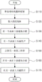
首先,可以准备绕组线圈10和框架40(S110)。First, the winding
接下来,可以将每个绕组线圈10装入框架40中的指定位置(S120)。Next, each winding
接下来,可以将绝缘粘合膜20-1涂覆在其中装有绕组线圈10的框架40的一个表面(例如,上表面)上(S130)。例如,可以将绝缘粘合膜20-1定位并随后压在框架40的一个表面上。Next, the insulating adhesive film 20-1 may be coated on one surface (for example, an upper surface) of the
接下来,可以将至少一个磁性片30-1定位并随后压在其上涂覆有绝缘粘合膜20-1的框架40的一个表面上(S140)。如上所述,根据本公开中的示例性实施例,绕组线圈10与框架40之间的连接性可以通过绝缘粘合膜得到充分保证,从而可以防止在压磁性片30-1时线圈错位。因此,根据本公开中的示例性实施例,良率可以得到改善。Next, at least one magnetic sheet 30-1 may be positioned and then pressed on one surface of the
接下来,可以去除贴附在框架40的另一个表面上的带(S150)。如上所述,根据本公开中的示例性实施例,绕组线圈10和框架40之间的结合力通过绝缘粘合膜20-1增大,由此抑制框架40的分离。因此,根据本公开中的示例性实施例,良率可以得到改善。Next, the tape attached on the other surface of the
接下来,可以将绝缘粘合膜20-2涂覆在其中装有绕组线圈10的框架40的另一个表面(例如,下表面)上(S160)。例如,可以将绝缘粘合膜20-2定位并随后压在框架40的另一个表面上。Next, the insulating adhesive film 20-2 may be coated on the other surface (eg, the lower surface) of the
接下来,可以将至少一个磁性片30-2定位并随后压在其上涂覆有绝缘粘合膜20-2的框架40的另一个表面上(S170)。包括相应磁芯、相应绕组线圈以及相应绝缘粘合膜的单个结构可以与框架40分离,并且成为绕线电感器。因此,当各个结构与框架40分离时,可以形成多个线绕电感器。Next, at least one magnetic sheet 30-2 may be positioned and then pressed on the other surface of the
图5是用于解释根据本公开中另一示例实施例的绕线电感器的制造方法的流程图。FIG. 5 is a flowchart for explaining a method of manufacturing a wire wound inductor according to another example embodiment in the present disclosure.
下面将参照图3和图5来描述根据本公开中的示例性实施例的绕线电感器的制造方法。A method of manufacturing a wire wound inductor according to an exemplary embodiment in the present disclosure will be described below with reference to FIGS. 3 and 5 .
首先,可以准备绕组线圈10和框架40(S210)。First, the winding
接下来,可以将每个绕组线圈10装入框架40中的指定位置(S220)。Next, each winding
接下来,可以将绝缘粘合膜20-1涂覆在其中装有绕组线圈10的框架40的一个表面(例如,上表面)上(S230)。例如,可以将绝缘粘合膜20-1定位并随后压在框架40的一个表面上。Next, the insulating adhesive film 20-1 may be coated on one surface (eg, an upper surface) of the
接下来,可以去除贴附在框架40的另一个表面上的带(S240)。如上所述,根据本公开中的示例性实施例,绕组线圈10和框架40之间的结合力通过绝缘粘合膜20-1增大,由此抑制框架40的分离。因此,根据本公开中的示例性实施例,良率可以得到改善。Next, the tape attached on the other surface of the
接下来,可以将绝缘粘合膜20-2涂覆在其中装有绕组线圈10的框架40的另一表面(例如,下表面)上(S250)。例如,可以将绝缘粘合膜20-2定位并随后压在框架40的另一个表面上。Next, the insulating adhesive film 20-2 may be coated on the other surface (eg, the lower surface) of the
接下来,可以通过激光加工来移除定位在绕组线圈10的中心部分的绝缘粘合膜20-1和20-2(S260)。可以通过在第一绝缘粘合膜20-1和第二绝缘粘合膜20-2的中心部分上照射激光束来执行激光加工,以去除第一绝缘粘合膜20-1和第二绝缘粘合膜20-2的中心部分。Next, the insulating adhesive films 20-1 and 20-2 positioned at the center portion of the winding
接下来,可以将至少一个磁性片30-1定位并随后压在其上涂覆有绝缘粘合膜20-1的框架40的一个表面上(S270)。如上所述,根据本公开中的示例性实施例,绕组线圈10与框架40之间的连接性可以通过绝缘粘合膜得到充分保证,从而可以防止在压磁性片30-1时线圈错位。因此,根据本公开中的示例性实施例,良率可以得到改善。Next, at least one magnetic sheet 30-1 may be positioned and then pressed on one surface of the
接下来,可以将至少一个磁性片30-2定位并随后压在其上涂覆有绝缘粘合膜20-2的框架40的另一个表面上(S280)。包括相应磁芯、相应绕组线圈以及相应绝缘粘合膜的单个结构可以与框架40分离,并且成为绕线电感器。因此,当各个结构与框架40分离时,可以形成多个线绕电感器。Next, at least one magnetic sheet 30-2 may be positioned and then pressed on the other surface of the
如上所述,根据本公开中的例性实施例的绕线电感器及其制造方法,绕组线圈和磁芯之间的绝缘可以得到保证,与此同时,它们之间的结合力可以被加强,使得绕线电感器的耐用性可以增强。此外,在制造绕线电感器的工艺中,线圈与框架之间的连接性可以得到保证,从而可以减少由于线圈错位而引起的缺陷。另外,可以抑制框架与线圈的分离,从而可以减少在堆叠磁性片时框架分离的缺陷。As described above, according to the wire wound inductor and the manufacturing method thereof of the exemplary embodiments in the present disclosure, the insulation between the winding coil and the magnetic core can be ensured, and at the same time, the bonding force between them can be strengthened, The durability of the wire wound inductor can be enhanced. In addition, in the process of manufacturing the wire-wound inductor, the connectivity between the coil and the frame can be guaranteed, so that defects due to misalignment of the coil can be reduced. In addition, separation of the frame and the coil can be suppressed, so that a defect of separation of the frame when stacking the magnetic sheets can be reduced.
虽然以上已经示出和描述了示例性实施例,但是对于本领域技术人员而言明显的是,在不脱离由所附权利要求限定的本发明的范围的情况下,可以进行修改和变型。While exemplary embodiments have been shown and described above, it will be obvious to those skilled in the art that modifications and variations can be made without departing from the scope of the invention as defined in the appended claims.
Claims (15)
Applications Claiming Priority (3)
| Application Number | Priority Date | Filing Date | Title |
|---|---|---|---|
| KR10-2017-0180143 | 2017-12-26 | ||
| KR1020170180143A KR102505437B1 (en) | 2017-12-26 | 2017-12-26 | Wire wound inductor and manufacturing method thereof |
| CN201811097372.5A CN109961920B (en) | 2017-12-26 | 2018-09-19 | Wound inductor and method of manufacturing the same |
Related Parent Applications (1)
| Application Number | Title | Priority Date | Filing Date |
|---|---|---|---|
| CN201811097372.5A Division CN109961920B (en) | 2017-12-26 | 2018-09-19 | Wound inductor and method of manufacturing the same |
Publications (2)
| Publication Number | Publication Date |
|---|---|
| CN115424812A true CN115424812A (en) | 2022-12-02 |
| CN115424812B CN115424812B (en) | 2025-12-02 |
Family
ID=66949612
Family Applications (2)
| Application Number | Title | Priority Date | Filing Date |
|---|---|---|---|
| CN201811097372.5A Active CN109961920B (en) | 2017-12-26 | 2018-09-19 | Wound inductor and method of manufacturing the same |
| CN202211218293.1A Active CN115424812B (en) | 2017-12-26 | 2018-09-19 | Wire-wound inductors and their manufacturing methods |
Family Applications Before (1)
| Application Number | Title | Priority Date | Filing Date |
|---|---|---|---|
| CN201811097372.5A Active CN109961920B (en) | 2017-12-26 | 2018-09-19 | Wound inductor and method of manufacturing the same |
Country Status (3)
| Country | Link |
|---|---|
| US (1) | US11538624B2 (en) |
| KR (1) | KR102505437B1 (en) |
| CN (2) | CN109961920B (en) |
Families Citing this family (3)
| Publication number | Priority date | Publication date | Assignee | Title |
|---|---|---|---|---|
| JP2021064669A (en) | 2019-10-11 | 2021-04-22 | 株式会社村田製作所 | Coil and inductor including coil |
| JP7493953B2 (en) * | 2020-02-17 | 2024-06-03 | 日東電工株式会社 | Inductor with frame member and laminated sheet with frame member |
| CN120199580B (en) * | 2025-05-27 | 2025-09-26 | 东莞市健阳达电子有限公司 | A limitable electronic transformer |
Citations (6)
| Publication number | Priority date | Publication date | Assignee | Title |
|---|---|---|---|---|
| CN104517710A (en) * | 2013-10-07 | 2015-04-15 | 三星电机株式会社 | Coil component |
| CN104575935A (en) * | 2013-10-11 | 2015-04-29 | 三星电机株式会社 | Inductor and its manufacturing method |
| CN104700982A (en) * | 2013-12-04 | 2015-06-10 | 三星电机株式会社 | Chip electronic component and manufacturing method thereof |
| CN104766691A (en) * | 2014-01-07 | 2015-07-08 | 三星电机株式会社 | Chip electronic component and manufacturing method thereof |
| CN104900374A (en) * | 2014-03-07 | 2015-09-09 | 三星电机株式会社 | Chip electronic component and manufacturing method thereof |
| US20160268040A1 (en) * | 2015-03-09 | 2016-09-15 | Samsung Electro-Mechanics Co., Ltd. | Coil electronic component and method for manufacturing the same |
Family Cites Families (36)
| Publication number | Priority date | Publication date | Assignee | Title |
|---|---|---|---|---|
| US7012784B2 (en) * | 1999-07-08 | 2006-03-14 | Tdk Corporation | Thin-film magnetic head and method of manufacturing same |
| JP2004040001A (en) | 2002-07-05 | 2004-02-05 | Taiyo Yuden Co Ltd | Coil component and circuit device |
| JP2005347542A (en) | 2004-06-03 | 2005-12-15 | Sony Corp | Multilayer coil and method of manufacturing multilayer coil |
| WO2006121518A2 (en) * | 2005-05-10 | 2006-11-16 | Angiotech International Ag | Electrical devices, anti-scarring agents, and therapeutic compositions |
| KR101153954B1 (en) | 2005-12-27 | 2012-06-08 | 주식회사 비즈모델라인 | Sticker with Contactless IC Chip and Method for Manufacturing Sticker |
| JP4600688B2 (en) * | 2007-03-29 | 2010-12-15 | Tdk株式会社 | Electronic component manufacturing method and electronic component |
| JP2011071457A (en) * | 2008-12-22 | 2011-04-07 | Tdk Corp | Electronic component and manufacturing method of electronic component |
| KR20180103174A (en) * | 2010-12-01 | 2018-09-18 | 파나소닉 주식회사 | Non-contact Charging Module and Non-contact Charging Instrument |
| KR101397488B1 (en) * | 2012-07-04 | 2014-05-20 | 티디케이가부시기가이샤 | Coil component and method of manufacturing the same |
| US9190380B2 (en) * | 2012-12-06 | 2015-11-17 | Intel Corporation | High density substrate routing in BBUL package |
| KR101414987B1 (en) | 2012-12-26 | 2014-07-08 | (주)창성 | Manufacturing method of the multilayered chip inductor |
| KR101442402B1 (en) * | 2013-03-25 | 2014-09-17 | 삼성전기주식회사 | Inductor and method for manufacturing the same |
| US9490656B2 (en) * | 2013-11-25 | 2016-11-08 | A.K. Stamping Company, Inc. | Method of making a wireless charging coil |
| GB2538459B (en) * | 2014-03-04 | 2020-09-23 | Murata Manufacturing Co | Coil component, coil module, and method for manufacturing coil component |
| TWI653312B (en) * | 2014-03-11 | 2019-03-11 | 日商味之素股份有限公司 | Film |
| KR102080660B1 (en) * | 2014-03-18 | 2020-04-14 | 삼성전기주식회사 | Chip electronic component and manufacturing method thereof |
| KR102004790B1 (en) * | 2014-05-08 | 2019-07-29 | 삼성전기주식회사 | Common mode filter and manufacturing method thereof |
| KR101627134B1 (en) | 2014-09-23 | 2016-06-03 | 삼성전기주식회사 | Common Mode Filter |
| KR102185067B1 (en) * | 2014-09-24 | 2020-12-01 | 삼성전기주식회사 | Coil unit for thin film inductor, manufacturing method of coil unit for thin film inductor, thin film inductor and manufacturing method of thin film inductor |
| KR102064027B1 (en) * | 2014-10-31 | 2020-01-09 | 삼성전기주식회사 | Sheet type inductor |
| US10468184B2 (en) * | 2014-11-28 | 2019-11-05 | Tdk Corporation | Coil component having resin walls and method for manufacturing the same |
| US20160276088A1 (en) | 2015-03-18 | 2016-09-22 | Samsung Electro-Mechanics Co., Ltd. | Wire wound inductor and method of manufacturing the same |
| KR20170003199A (en) * | 2015-06-30 | 2017-01-09 | 삼성전기주식회사 | Thin film type coil component and method of manufacturing the same |
| JP6825189B2 (en) | 2015-07-29 | 2021-02-03 | サムソン エレクトロ−メカニックス カンパニーリミテッド. | Coil parts and their manufacturing methods |
| KR101832598B1 (en) * | 2015-07-29 | 2018-02-27 | 삼성전기주식회사 | Coil component and manufacturing method for the same |
| KR101762039B1 (en) * | 2015-12-18 | 2017-07-26 | 삼성전기주식회사 | Coil component |
| KR101792365B1 (en) | 2015-12-18 | 2017-11-01 | 삼성전기주식회사 | Coil component and manufacturing method for the same |
| US9842788B2 (en) * | 2015-12-31 | 2017-12-12 | Taiwan Semiconductor Manufacturing Company, Ltd. | Underfill control structures and method |
| KR101792388B1 (en) | 2016-01-28 | 2017-11-01 | 삼성전기주식회사 | Coil component and manufacturing method for the same |
| KR101823267B1 (en) * | 2016-11-01 | 2018-01-29 | 삼성전기주식회사 | Thin film inductor and method of fabricating the same |
| KR20160134633A (en) | 2016-11-17 | 2016-11-23 | 삼성전기주식회사 | Wire wound inductor and manufacturing method thereof |
| KR101892822B1 (en) * | 2016-12-02 | 2018-08-28 | 삼성전기주식회사 | Coil component and manufacturing method for the same |
| US10211137B2 (en) * | 2017-06-08 | 2019-02-19 | Advanced Semiconductor Engineering, Inc. | Semiconductor device package |
| KR101983191B1 (en) * | 2017-07-25 | 2019-05-28 | 삼성전기주식회사 | Inductor and method for manufacturing the same |
| KR102064041B1 (en) * | 2017-12-11 | 2020-01-08 | 삼성전기주식회사 | Coil component |
| JP7021599B2 (en) * | 2018-04-18 | 2022-02-17 | 株式会社村田製作所 | Common mode choke coil |
-
2017
- 2017-12-26 KR KR1020170180143A patent/KR102505437B1/en active Active
-
2018
- 2018-06-08 US US16/004,104 patent/US11538624B2/en active Active
- 2018-09-19 CN CN201811097372.5A patent/CN109961920B/en active Active
- 2018-09-19 CN CN202211218293.1A patent/CN115424812B/en active Active
Patent Citations (7)
| Publication number | Priority date | Publication date | Assignee | Title |
|---|---|---|---|---|
| CN104517710A (en) * | 2013-10-07 | 2015-04-15 | 三星电机株式会社 | Coil component |
| CN104575935A (en) * | 2013-10-11 | 2015-04-29 | 三星电机株式会社 | Inductor and its manufacturing method |
| CN106449011A (en) * | 2013-10-11 | 2017-02-22 | 三星电机株式会社 | Inductor |
| CN104700982A (en) * | 2013-12-04 | 2015-06-10 | 三星电机株式会社 | Chip electronic component and manufacturing method thereof |
| CN104766691A (en) * | 2014-01-07 | 2015-07-08 | 三星电机株式会社 | Chip electronic component and manufacturing method thereof |
| CN104900374A (en) * | 2014-03-07 | 2015-09-09 | 三星电机株式会社 | Chip electronic component and manufacturing method thereof |
| US20160268040A1 (en) * | 2015-03-09 | 2016-09-15 | Samsung Electro-Mechanics Co., Ltd. | Coil electronic component and method for manufacturing the same |
Also Published As
| Publication number | Publication date |
|---|---|
| CN109961920A (en) | 2019-07-02 |
| KR20190078298A (en) | 2019-07-04 |
| KR102505437B1 (en) | 2023-03-03 |
| US11538624B2 (en) | 2022-12-27 |
| US20190198235A1 (en) | 2019-06-27 |
| CN115424812B (en) | 2025-12-02 |
| CN109961920B (en) | 2022-10-21 |
Similar Documents
| Publication | Publication Date | Title |
|---|---|---|
| JP6181133B2 (en) | Coil component assembly, coil component and manufacturing method thereof | |
| JP6071945B2 (en) | Inductor and manufacturing method thereof | |
| JP5557902B2 (en) | Magnetic component assembly | |
| US11769621B2 (en) | Inductor with an electrode structure | |
| CN110544577B (en) | Coil component and electronic device | |
| US20130300529A1 (en) | Coil structure and electromagnetic component using the same | |
| KR101823191B1 (en) | Chip electronic component and manufacturing method thereof | |
| JP6230972B2 (en) | Chip electronic component and manufacturing method thereof | |
| JPH10172832A (en) | Wound electronic parts | |
| JP6614207B2 (en) | Coil component assembly, coil component and manufacturing method thereof | |
| JP2017069460A (en) | Coil component and manufacturing method therefor | |
| JP2005327876A (en) | Coil component and its manufacturing method | |
| KR102016497B1 (en) | Coil component | |
| CN107851503A (en) | Flexible inductor | |
| CN109961920B (en) | Wound inductor and method of manufacturing the same | |
| JP6716867B2 (en) | Coil component and manufacturing method thereof | |
| US11610726B2 (en) | Coil device and pulse transformer | |
| US11848138B2 (en) | Coil component and method for manufacturing coil component | |
| US11657956B2 (en) | Coil device and pulse transformer | |
| CN110277230B (en) | Coil component | |
| KR20160026940A (en) | Coil component | |
| WO2022065027A1 (en) | Coil component and method for manufacturing same | |
| KR101952867B1 (en) | Coil component and method for manufacturing same | |
| CN111161945A (en) | Coil electronic component | |
| US11923118B2 (en) | Coil component and method of manufacturing coil component |
Legal Events
| Date | Code | Title | Description |
|---|---|---|---|
| PB01 | Publication | ||
| PB01 | Publication | ||
| SE01 | Entry into force of request for substantive examination | ||
| SE01 | Entry into force of request for substantive examination | ||
| GR01 | Patent grant | ||
| GR01 | Patent grant |