Here narrate a kind of MULTI-VALUED LOGIC CIRCUIT structure and obtain the method for this structure.Additional symmetrical logic circuit structure disclosed herein (SUS-LOC) mainly is intended for use design and makes base (r) greater than 2 full active logic circuit.The SUS-LOC structure can be used to realize any r value logic function of n position, and order and the desired element of clock sequential logic, and wherein basic r is the integer greater than 1, and n is the integer greater than 0.
Open by the prior art that U.S.Patent and Trademark Office Document DisclosureProgram makes, here by its reference is introduced clearly.The U.S.Patent Application Serial Number09/086 that submitted on May 29th, 1998,869, here by to it with reference to introducing, the confidentiality of described patent application or any application relevant with it is not abandoned.Here symbol of Ti Chuing and term further developing and may stand to change with multi valued logic and SUS-LOC structure.
The previous logical construction of past 50 years exploitation almost ad hoc contributes to the synthetic of binary logic, and they comprise: transistor-transistor logic (TTL); P raceway groove and N NMOS N-channel MOS N (PMOS﹠amp; NMOS); With complement code symmetry metal-oxide semiconductor (MOS) (be initially COS-MOS, current is CMOS).
Why not exploitation can be supported the logical construction that logic function is synthesized except that binary system in the past, and its most of reason is speculative at the most only, still may comprise: occupied by binary logic in advance; Imagination realizes that higher base will be too complicated or expensive; And binary system was before achieved success.
There are two not to be speculative reason.The firstth, the cost effective ways of unavailable generation in the past and detection intermediate logic level.The second, can realize one can the combinator function circuit (particularly full active circuit) before, be used to design and make circuit structure rule and limit and must satisfy three requirements.These three requirements are:
1) must have r power supply to use, each power supply is only represented in r the Different Logic level;
2) output from a power supply to the circuit of each output logic level must have a controlled path or branch; And
3) from a power supply to each input logic level, the output of the input logic level of contiguous input logic level group or unique combination, the conduction of a controlled path or branch is only arranged.
By " replenishing ", all these three requirements are satisfied in SUS-LOC structure Design rule and qualification.Allow only to use binary switch (for example transistor) like this, design and the full active circuit of making any r value logic function circuit that to synthesize the n position economically.
Feature output characteristic based on the SUS-LOC circuit is determined by the standard of used switch.Manufacturing based on the SUS-LOC circuit can be finished with about 1970 technology, material and facility.Yet latest developments energy and the present invention of circuit engineering advantageously are applied together.And the advantage of ternary logic is not the restriction of SUS-LOC structure among the present invention, but to the result of general service computer optimization, and follow to provide stable rule than simple components to most advanced and sophisticated and complication system.
Under the simple scenario of " bit function " (hereinafter), " replenishing " is the technology that is used to realize stablizing intermediate logic/voltage level.For example, for ternary complementer F210, a switch is used for each of two terminal logic level.Two switches are connected to the series connection conduction, and share a control signal altogether, and the terminal of each intermediate logic level " is replenished " terminal, each output logic level above two of each input item.Two switches of intermediate logic level define upper and lower input signal, and these two signals produce the output response of intermediate logic level.
The several advantages that base obtained that increase logic synthesis circuit include but not limited to: reduce static and dynamic power requirement, increase packing density, and increase computing capability.
For the switch of SUS-LOC structure choice of the present disclosure is that (IGFET, FET), this is because their low cost, high reliability and be easy to make former thereby cause to isolated-gate field effect transistor (IGFET).Yet the switch of any similar characteristics can be suitable replacement, such as but not limited to igbt or simulated light device.
Make and select channel type, model and the threshold voltage (V of each FET
GS (TH)), when connecting with branch of box lunch, every other branch disconnects.Just, when at least one switch in the every other branch disconnected, all switches in branch were all connected.For a bit function (OPF), when arbitrary terminal branch was connected, at least one FET of another terminal branch and each medial fascicle disconnected.In addition, when a medial fascicle was connected, at least one FET in two terminal branch and the every other medial fascicle disconnected.Therefore, for any unique input, only transmit a unique output.This situation all is true for any input number.
Basic circuit elements: IGFET
In the present invention, (IGFET FET) constitutes the SUS-LOC circuit with isolated-gate field effect transistor (IGFET).IGFET is known in the art, and it has source S, grid G and drain D.Very usually, according to the grid input control voltage that is applied on the IGFET, IGFET not only allows but also prevents the transmission of source voltage to drain electrode.Source voltage is to the transmission that drains or do not transmit the relative voltage that depends between source voltage and grid or the input voltage.The operating characteristic that depends on concrete IGFET and selection thereof, the grid input control voltage may be higher or lower than source voltage.
Have these operating characteristics, IGFET highly is applicable to SUS-LOC.Selectively, other devices may utilize these devices as the replacement of IGFET, and control voltage (or input) can allow and can prevent the not only transmission of low but also higher than control voltage source voltage than control voltage.Application Optics Progress in technique, the optical analog of IGFET may become available, and play the substitution of IGFET.Optical analog or quantum device, for example " super logical " transistor can solve the reverse bias problem that IGFET suffered among the SUS-LOC." super logical " transistor is by X.Deng, T.Hanyu and M.Kameyama are open in their article " Quantum DeviceModel Based Super Pass Gate for Multiple-Valued Digital ", this article is submitted in " 25th International Symposium on Multiple-ValuedLogic (ISMVL), 1995 ".
Fig. 1 and Fig. 2 represent the enhancement mode FET of P raceway groove and N channel type respectively.Fig. 3 and Fig. 4 represent the depletion type FET of P raceway groove and N channel type respectively.Fig. 5 represents nearly zero threshold value FET.For each FET that is not nearly zero threshold value FET, the grid that is right after each FET is one "+V " or " V ", is used to indicate the threshold voltage V of the source voltage of relative FET
GS (TH)Polarity and size.In this patent, V
GS (TH)Also be called V
GS onAnd V
GS off, to indicate the on-off action of enhancement mode and depletion type FET respectively.
For enhancement transistor (Fig. 1 and Fig. 2), voltage crosses gate threshold voltage (V when the relative source of grid input voltage
GS off) time, transistor is connected.For depletion mode transistor (Fig. 3 and Fig. 4), voltage crosses gate threshold voltage (V when the relative source of grid input voltage
GS off) time, transistor disconnects.Fig. 7 a to Fig. 7 f represents these response characteristics with diagram form.
A kind of method of understanding IGFET operation is to consider that the initial and source voltage of grid input voltage is in the situation of same level.The relative source of gate threshold voltage voltage will be ± V, and be that what how to make is constant according to FET.Usually, when the input gate voltage equaled source voltage, enhancement mode IGFET disconnected, and depletion type IGFET connects.The grid input voltage increases or reduces, so that (source voltage adds V near absolute gate threshold voltage
GS (TH), or source voltage subtracts V
GS (TH)).When crossing absolute gate threshold voltage, IGFET will be according to its pre-selected characteristics operation.For enhancement mode IGFET, IGFET connects, and source voltage is transmitted to drain electrode.For depletion type IGFET, IGFET disconnects, and source voltage is not transmitted to drain electrode.
Fig. 1 represents to have-the gate threshold voltage V of V
GS onThe P-channel enhancement type transistor.Item V
GS onIndicate relative gate threshold voltage, the P-channel enhancement type transistor is connected under this voltage.Relative voltage is grid input voltage and source voltage.If grid input voltage and source voltage phase difference had at least-the gate threshold voltage V of V
GS on, the P-channel enhancement type transistor is connected, and source voltage will be transmitted to drain electrode.If gate voltage and source voltage phase difference are less than-V, the P-channel enhancement type transistor disconnects, and does not have the conduction generation between source electrode and drain electrode.The present invention uses the P-channel enhancement type transistor, with when grid input voltage during than the little gate threshold voltage of source voltage, source voltage is transmitted to drain electrode.Relative gate threshold voltage (V between grid and the source voltage
GS on) control by changing transistorized doping level and other characteristics (for example oxide thickness) during manufacture.These operating characteristics of P-channel enhancement type IGFET correspondingly and to be used for other IGFET of the present invention similar.
Fig. 2 represents the N channel enhancement transistor, it has+and the relative gate threshold voltage V of V
GS onIf grid input voltage and source voltage phase difference at least+V, the N channel enhancement transistor is connected, and source voltage will be transmitted to drain electrode.Otherwise transistor disconnects.The present invention uses the N channel enhancement transistor, with when grid input voltage during than the high relatively gate threshold voltage of source voltage, source voltage is passed to drain electrode.
Fig. 3 represents the P channel depletion mode transistor, it has+and the relative gate threshold voltage V of V
GS offIf grid input voltage and source voltage phase difference at least+V, the P channel depletion mode transistor disconnects, and will not have the conduction generation between source electrode and drain electrode.Otherwise transistor is connected, and will pass to its drain electrode to the voltage of its source electrode.The present invention uses the P channel depletion mode transistor, with when grid input voltage during than the high relatively gate threshold voltage of source voltage, source voltage and drain electrode is disconnected.
Fig. 4 represents the N channel depletion mode transistor, it has-and the gate threshold voltage V of V
GS offIf grid input voltage and source voltage phase difference at least-the gate threshold voltage V of V
GS off, the N channel depletion mode transistor disconnects, and will not have the conduction generation between source electrode and drain electrode.If gate voltage and source voltage phase difference are less than-V, the N channel depletion mode transistor is connected, and will source electrode with drain between conduct.The present invention uses the N channel depletion mode transistor, with when grid input voltage during than the low gate threshold voltage of source voltage, source voltage and drain electrode is disconnected.
The P channel fet is useful in the upper limit that limits SUS-LOC branch, and the N channel fet is useful in the lower limit that limits SUS-LOC branch.By selectively limiting the conduction band, make them have the upper and lower bound that is limited as P raceway groove and N channel fet, then can design the logical circuit function of any digital system (basic r), it has any input number (n).
Because the usually open circuit element that is comprised of circuit symbol, so follow the accompanying drawing of this patent usually to be used as the complete open of the SUS-LOC circuit shown in it.In addition, accompanying drawing utilizes this structural system with the open the present invention of a kind of structural system, can realize the majority circuit and the application of multi valued logic.
Because SUS-LOC structure of the present disclosure is used FET,, the protection input wishes so exempting from Electrostatic Discharge.Fig. 6 represents to protect input to avoid a kind of method of ESD.Also can use additive method.
The minimum and maximum supply voltage (output voltage) of SUS-LOC circuit is required by the output of circuit and the standard of the switch that uses is determined.Yet to logic level 0 and 1, the minimum power source voltage of suggestion is respectively 0.0 volt and 1.5 volts.So each additional logic level can be last logic-level voltages adds logic level 1 voltage, so that 1.5 volts logic stepped voltage (LSV) to be provided.Importantly keep the discrete logic level in digital application, 1.5 volts are counted as easy realization.Also can use other LSV values to obtain good result.
Employed power indicator is to have target character " V " under the logic level simply in the schematic diagram of SUS-LOC circuit, and logic level is represented (V for example by this voltage
1 Presentation logic level 1, V
3 Presentation logic level 3 etc.).
Because the high input impedance of FET, and because each output supply voltage is only represented in r the Different Logic level, so the logic level of SUS-LOC circuit equals the supply voltage of presentation logic level in fact.As described below, for each level of r Different Logic level, voltage range or territory are set up according to predictable relationship.
Select or make the threshold voltage V of P channel fet
GS (TH), so that the percentage of its logic level that to be the highest input logic level that will conduct than FET high.Select or make the threshold voltage V of N raceway groove
GS (TH), so that the percentage of its logic level that to be minimum input logic level that will conduct than FET low.Should be in 55% to 75% scope of logic stepped voltage (LSV) to the percentage of suggestion separately, during to another, obtain the stack in branch from an output logic level conversion with convenient circuit.This percentage is called " stack percentage " (OP), and should be identical for all switches that are used for digital application.Simulation application may require V
GS (TH)And/or OP and/or LSV are variable.
When as suggestion, using OP, kept circuit symmetry, because the mid point of logic level switching point voltage between two adjacent logic levels voltage.Owing to during switch,, the output transmission characteristic is improved to output continuous application voltage.Each logic level is set up a territory, and its border is by the upper and lower switching point voltage of medial fascicle, and the switching point voltage and the V of terminal branch
0Or V
R-1Set up.
When logic function of exploitation or logic synthesis circuit (" logic function "), must calculate threshold voltage suitable or that require to each FET.In order to calculate the V of a specific FET
GS (TH), according to the channel type of FET, from following two formula, select a suitable formula:
P raceway groove: V
GS (TH)=Vi-(VO-(OP * LSV)); And
N raceway groove: V
GS (TH)=Vi-(VO+ (OP * LSV)).
Wherein:
Vi is the input logic level voltage limit (suitably being the upper limit or lower limit) that branch responds;
VO is the output logic level voltage;
LSV is the logic stepped voltage; And
OP is the selective stacking percentage in 55% to 75% scope preferably.
Because logic level territory, switch and the tolerance limit of power supply, the high impedance of FET, and stack percentage causes, the noise immunity of SUS-LOC circuit from a logic level about 45% to several logic levels.The output of some function changes a logic level with the input of two or more logic levels, so the noise immunity performance among the SUS-LOC is in several logic level scopes.
The response input stimulus is so that output and any circuit element that a power supply is connected/disconnects are named as a branch, to narrate and to name particular element among the present invention better.The SUS-LOC structure comprises two kinds of main branch patterns, is appointed as " terminal " and " centre " and a kind of less important branch pattern, is appointed as " compound ".
Terminal branch
All logic functions require minimum two terminal branch.The existence of medial fascicle and computing method are determined by base that is synthesized and specific logical function.When logic function required two or more input item, compound branch was combined to form by main branch.The logic function of getting two or more input items like this is also referred to as multidigit function (MPF).The following qualification of each branch pattern.
A terminal branch is made up of a FET, and it is connected an output with the power supply of a presentation logic level, and cycle through logic level sequence 0 when input ... during r-1, it responds to one or one group of adjacent logic levels.
The FET that is used to form terminal branch depends on the input logic level of (I) response output logic level (O) to branch.Channel type (P or N) and model are that enhancement mode or depletion type (E or D) are:
For I>O, use NE;
For I<O, use PE.
In other words, when response input (I) never equals output (O), use enhancement mode FET.In addition, when I equals O (I=O), FET disconnects or conducts so that export.This is consistent with enhancement mode FET characteristic.When I>O, use N type enhancement mode FET.When I<O, use P type enhancement mode FET.Have such terminal OPF one be illustrated in F201 among Figure 89.
When following condition all exists, in terminal branch, can use depletion type FET.
1. be not 0 or r-1 for this FET output logic level;
2. require the output logic level for two or more adjacent input logic levels;
3. output is to comprise 0 or the element of the input logic level sequence of r-1;
4. Shu Ru big young pathbreaker's plus or minus ground (+or-) surpasses the output logic level;
5. the size of output logic level is not surpassed by another output logic level; And
6. another terminal branch FET is enhancement mode FET.
When above-mentioned six conditions existed, employed channel type was as follows:
To conduct when depletion type FET response input logic level 0 and 1 (or 0 and>0, depend on base), and when not having other output logic level, use P channel depletion type FET so greater than the output logic level that conducted by this depletion type FET.The example of this situation is the F110 shown in Figure 71
3
When depletion type FET response input logic level r-1 and r-2 (or r-1 and<r-1, depend on base) and will conduct, and when not having other output logic level, use N channel depletion type FET so less than the output logic level that conducted by this depletion type FET.The example of this situation is the F211 shown in Figure 98
3
Should be noted that given rule attempts to provide firm and reliable indication and nomenclature here, can make the present invention be put to use and put into practice thus.
Medial fascicle
A medial fascicle is made up of two FET that are connected in series, they are connected an output with a power supply, this power supply is represented by a logic level between the logic level of terminal branch conduction, and when input cycles through logic level sequence 0, ... during r-1, this medial fascicle is to one or one group of adjacent input logic level response.
Can use three kinds of possible FET to make up and form a medial fascicle.Specific FET combination is depended on the input logic level of (I) response output logic level (O) to branch.Channel type P or N and model are being combined as of enhancement mode or depletion type (E or D):
For O>I, use PE﹠amp; ND;
For O ∈ I, use PD﹠amp; ND; And
For O<I, use PD﹠amp; NE.
Wherein: PE represents P-channel enhancement type;
NE represents the N channel enhancement;
PD represents the P channel depletion type; And
ND represents N channel depletion type FET.
For example, the quinary shown in Figure 110 (base 5) base-1 complementer comprises all these three kinds of combinations.
This three kinds of FET combination define window or the band gap that two FET conduct separately.Under the situation of conduction band, use PE and ND for the input of the response under output logic level O I generation.For the conduction band of about O, use PD and ND.For the conduction band on the O, use PD and NE.
Compound branch
A compound branch is the combination of several terminals and/or medial fascicle, comes across the requirement of multidigit logic function wherein according to them, connects into series, parallel or connection in series-parallel conduction.Compound branching out in the present multidigit function like this, and in a bit function, do not exist.For example, the CGOR of Fig. 8
3The CGAND of circuit and Fig. 9
3Circuit respectively has three branches, and the CEQ of Figure 10
3Circuit has five branches.
The relation of the conduction of branch and non-conducting input logic level and output logic level is determined model and the channel type of the FET of this branch of formation.
Reverse bias
FET allows the bidirectional current between source electrode and drain electrode.For the P channel fet, more positive electrode will play the source electrode effect.For the N channel fet, more negative electrode will play the source electrode effect.Because source electrode and drain electrode are determined by polarity that places the voltage on them and/or size, so a bit function and multidigit function both often require adjunct circuit to prevent " reverse bias ".For a bit function, adjunct circuit " level " is used to realize suitable circuit output.For the multidigit function, an additional bit function (OPF) may be used for one or more inputs, with not only during its on-state but also during off-state, guarantees that the suitable input logic level of branch responds the output logic level.
When the output logic level changes with the relative direction with input logic level, do not require extra level or OPF.For example, reduce (for example for complementer), need not adjunct circuit if output increases with input.Yet, when the relative input logic level of output logic level with arbitrary equidirectional rather than relative direction, or when changing randomly, require extra level or OPF so.Owing to may require identical extra level more than one branch or circuit element, as needs so the output of such level or OPF and/or input may feedover.
Because those of ordinary skill major concern binary inverter, NOR, NAND and the xor logic function of binary logic, so simulation ternary logic function is interesting especially, and following narration.Yet, also can finish the structure and the realization of other r value functions, and be put to good use.In these circuit some provides advantage and signal handling capacity unavailable in the binary system.Usually, SUS-LOC can adapt to any radix (r in any combination
1, r
2... r
n).In addition, the how basic circuit with two or more inputs also within the scope of the invention.The basic function circuit can use single basic r in a circuit with one or more inputs.
The exploitation of r value SUS-LOC circuit is one four a step process.This four step is:
STEP 1:
Limit the parameter of circuit:
A. determine the base of function;
B. determine or selection logic-level voltages and logic stepped voltage (LSV); And
C. determine or selective stacking percentage (OP).
STEP 2:
The Karnaugh map of the function that exploitation is developed.To the those of ordinary skill of two-valued function functional development, this is a known procedure.Unique not being both depended on graphic specific logical function, when the base of function greater than 2 the time, diagram generally will comprise the value greater than 1.
STEP 3:
According to the Karnaugh map of STEP 2 exploitations, list the logical relation of input item logic level and output logic level.This step is known to the those of ordinary skill of binary logic exploitation.Yet, when base greater than 2 the time, single input obtains the relation property of multidigit binary functions, such relation property comprises: equal, greater than, be equal to or greater than, these functions reciprocal, with and arrange.
Because equate that than simple more complicated relational operation is possible in the synthetic original level of SUS-LOC logic, thus during the realization of STEP 3, just should use such relational operator as possible, to guarantee maximum circuit efficiency.
STEP 4:
According to the information of step 1,2 and 3 acquisitions, design circuit.
Below narrate an example of the realization in these steps.
Following parameters (it is simple to be chosen as maintenance threshold value and logic-level voltages mathematics) is used to develop the ternary circuit of representing and narrating here:
V
2=5.0 volts
V
1=2.5 volts
V
0=0.0 volt
OP=71%
Can following exploitation binary radix-1 complementer or inverter.Because the above parameter (step 1) that defines in parameter limits, so exploitation is proceeded from going on foot 2, it comprises the Karnaugh map shown in the Table A.
Table A
The logical relation of input item/input and output logic level/output is developed and listed to step 3.The realization in step 3 obtains the listed relation of tabulation B down:
Inspection to relation indicates, and each input logic level output is changed.This meaning has three branches, two terminal branch and a medial fascicle.
Step 4 is proceeded the exploitation of logic function.At first be the branch that transmits output logic level 0, and set up the branch that transmits output logic level r-1 (r-1=2 under this situation), go on foot 4 following carrying out.
To output (O) logical zero, the input (I) with logic 2, output logic level ratio terminal branch is low to the minimum input logic level of its response.Point out use N channel enhancement FET like this.Use the formula (above) of the N channel device of threshold voltage determining section, and use 2.5 volts logic stepped voltage and 70% superimposed voltage, obtain V
GS (TH):
Vi Vo OP LSV V
GS(TH)
5 volts-(0 volt+(0.7 * 2.5 volt))=+ 3.75 volts
This FET is expressed as Q4 in Figure 95.
Next develops medial fascicle.Under this situation, only have one, and it must response logic 1 input, logical one output is provided.Point out to require a P channel depletion type FET and a N channel depletion type FET (, to use PD﹠amp like this for O ∈ I; ND).To P raceway groove and N channel device, use the threshold value formula, obtain following V
GS (TH)Voltage:
The P channel depletion type:
Vi Vo OP LSV V
GS(TH)
2.5 volt-(2.5 volts-(0.7 * 2.5 volt))=+ 1.75 volts
The N channel depletion type:
Vi Vo OP LSV V
GS(TH)
2.5 volt-(2.5 volts+(0.7 * 2.5 volt))=-1.75 volts
These two FET are expressed as Q2 and Q3 (their position can exchange) in the bit function as this function in Figure 95.
For the input to logic level 0 provides the output of logic 2, output logic level ratio terminal branch is big to the highest input logic level of its response, and P-channel enhancement type FET is used in indication.P-channel device is used formula, obtain V
GS (TH):
Vi Vo OP LSV V
GS(TH)
0 volt-(5 volts+(0.7 * 2.5 volt))=-3.75 volts
This FET is expressed as Q1 in Figure 95.
Be used to develop the method for the branch of ternary base-1 complementer, effective for all branches of any r value logic function of any figure place of exploitation.This method can expand to and adapt to additional medial fascicle.
SUS-LOC provides preparation for the multidigit function development, and these multidigit functions allow to compare and other logical operation using the several inputs based on the logic level signal of same base r.Actual branch design (step 4) is developed described similar with above ternary base-1 complementer.For example of the present invention is provided, three ternary multidigit functions is narrated step 2, step 3 and gone on foot 4 result: complement code broad sense OR (CGOR
3), complement code broad sense AND (CGAND
3) equal generator (CEO with complement code
3).These three ternary functions are thought respectively with binary system " NOR ", class seemingly for " NAND " and " different " (" XOR ").
Ternary complement code broad sense OR
3Or CGOR
3Door and binary system " NOR " class are seemingly.CGOR
3The output logic level of door is base-1 complement code of supplying with the high logic level of its input.This is by the CGOR shown in the table C
3Karnaugh map indication (" A " and " B " imports).
Table C
Next lists the logical relation of input item logic level and output logic level.Table D only uses equal relational operator, expression CGOR
3Relation.As show shown in the D, in the circuit 9 compound branches will arranged as a result, and will require excessive transistor (greater than 8) to realize.In table D, " C " is the output for input " A " and " B ".
Table D
| A | B | C | A | B | C | A | B | C | |
| 0 | 0 | 2 | 0 | 1 | 1 | 0 | 2 | 0 |
| 1 | 0 | 1 | 1 | 1 | 1 | 1 | 2 | 0 |
| 2 | 0 | 0 | 2 | 1 | 0 | 2 | 2 | 0 |
Though can design function nine branch circuits, should use more complicated relational operator (for example greater than, or be equal to or greater than).CGOR shown in Figure 8
3Circuit designs with more complicated relational operator shown in the table E.
Table E
| A | B | C |
| =0 | =0 | =2 |
| =1 | <2 | =1 |
| =2 | x | =0 |
| <2 | =1 | =1 |
| x | =2 | =0 |
X=is indifferent to
As shown, 3 compound branches are arranged.This be since two " being indifferent to " inputs " x " be the part of the compound branch of same terminal, and=1 and<2 both inputs be combined into the centre compound branch.After this manner, only require 8 transistors.Shown in Fig. 8 mirage line, to CGOR
3Expansion only requires 4 transistors to adapt to more inputs to each input.
Ternary complement code broad sense AND or CGAND
3Circuit and binary system " NAND " class seemingly, its Karnaugh map be shown in the table F.
Table F
Fig. 9 represents the CGAND according to relational operator exploitation shown in the table G
3Circuit, it also only requires 8 transistors, and the exaptation additional input, and each additional input is only required 4 transistors.To the adaptation of such additional input by shown in Fig. 9 mirage line.
Table G
| A | B | C |
| =0 | x | =2 |
| x | =0 | =2 |
| =1 | ≥1 | =1 |
| ≥1 | =1 | =1 |
| =2 | =2 | =0 |
X=is indifferent to
Can equate generator or CEQ according to SUS-LOC design and structure ternary complement code
3CEQ
3Determine whether two input A and B equate, and to the consequential signal complement code.Yet, as shown in figure 10, CEQ
3According to the output requirement of circuit, rather than, transmit its output by at first producing the equal signal of complement code subsequently.
Table H represents CEQ
3Karnaugh map.This Karnaugh map indication CEQ
3Output sequence be not " reverse sequence " very as complementer.Indication CEQ is exported or exported at random to non-reverse sequence like this
3Circuit requirement adds OPF.Shaded area indication " non-reverse sequence " or " at random " output valve of table H.
Table H
In the relational operator that Table I is listed, also can see CEQ for additional OPF
3Requirement (equally shown in shaded area).
Table I
X=is indifferent to
Except that additional OPF, the branch of response A=1, B=1 input also requires two extra switch, and these two switches are in arbitrary logic 2 that is input as, and another is when being input as logical one, is driven by the output of additional OPF, to prevent unusual path (reverse bias).For A=2, B=1, Q5 and Q6 keep disconnecting (or conduction) by B=1.Q4 is disconnected by A=2.Q3 is P type FET, and is derived from positive electrode.Work as CEQ
3Circuit transmits V to A=2, B=1
2During output, this V
2Signal passes to Q3.When A=2 compares V
1Or V
2(it is V to middle the greater
2) big 1.75 volts the time, Q3 connects, and V
2Be transmitted to V
1Below will narrate so unusual path in more detail.
Additional OPF for A and B input is expressed as Q8 and Q9 and Q13 and Q14 respectively in Figure 10.These OPF are F110
3Below narrate the use of such OPF in more detail.Q11 and Q12 constitute one " doorkeeper ", to prevent V
2Output is to the reverse transmission of FET Q3 to Q6.
Complement code equates generator or CEQ
3Form by two " XOR " door and one " NOR " near binary equivalent.Represent that one 2 value is (to realizing CEQ because require two binary digits
39 may input states be necessary), so require two binary system XOR gate.Equating of two " XOR " indivedual binary digits of detection, and the input of " NOR " door is by the output driving of " XOR " door.The CMOS binary equivalent requires 24 transistors, and CEQ shown in Figure 10
3Only require 18 transistors.
Expansion forms the CEQ with 3 input items
3, require 12 extra transistor, to constitute 30 transistors altogether.Meaning can be determined 3 equating and greater than zero equal level in once-through operation like this.Three CEQ
3Can not determine in once-through operation that three equal unitary classes are like binary functions.With other aspects, SUS-LOC handles electronic information important expansion and big efficient is provided in this respect.
Make CGOR
3, CGAND
3And CEQ
3Desired number of transistors may surpass the number of transistors of corresponding binary ciruit, therefore, and as if too much.Yet these ternary doors have the combination of nine possible A and B input separately.Can have the similar binary ciruit of nine input states to require A and B input item is the multidigit value, and such circuit will require more transistor, more lead, and more I/O pin, and have more parasitic value than corresponding ternary circuit.
The general indication of different requirements, realization and synthetic computing capability between binary system and the ternary logic (in their original level), ternary (or higher base) system will require less transistor than equivalent binary system than complex logic.Yet so higher based system generally obtains higher computing capability.
Some warning is proposed when directly replacing binary ciruit with SUS-LOC.It is tempting replacing the binary system door with r value door, and will form functional circuit (if giving some attention to suitable triggering level) in some cases.Yet, use by the available logic function number of higher basic SUS-LOC circuit the design and the manufacturing of general preferred more specifically logic function.Design and make circuit with function more specifically and will reduce parts number, all power requirement, parasitic parameter etc., so that the realization of SUS-LOC even more favourable.
Unusual path
As mentioned above, unusual path can cause owing to the use of some circuit element, generally causes short circuit.In general, these problems are owing to FET is the most just getting (for the P raceway groove) or the most negative (for the N raceway groove) voltage this true causing of source voltage as them at source electrode or drain electrode.So becoming, the required gate voltage of control FET depends on the effect of which voltage origin voltage and gate threshold voltage.The ifs circuit output voltage has been occupied original source voltage, and the gate voltage of the initial source electrode of expection relatively control FET may keep this control inadequately.
For fear of such problem, in SUS-LOC, use the adjunct circuit level, transmit output signal to prevent commute in the FET of the source voltage that changes them.
In the Karnaugh map of this circuit,, indicated requirement to the additional logic level with non-reverse output sequence.That is to say, output in the relative direction of the combination of order input logic level or order input logic level not in proper order, or input and output all equal V
0Or V
R-1
When back kind situation occurring, input logic level does not have enough sizes, and to cross the threshold voltage of FET, this FET will be transmitted to output to suitable output logic level voltage.Just, 0 input is no more than the threshold voltage that is transmitted to the N channel fet of output to 0.Solution is to use OPF, 0 input is increased or be converted into high value, so that can cross threshold voltage by the output voltage of OPF.Similarly, when the input and output both be V
R-1The time, by using OPF, can realize similar adaptation.In this case, OPF can reduce V with transforming
R-1Input is so that can cross threshold voltage by the OPF output voltage.
For OPF, conventional, standard or Inverted Output sequence are such sequences, and when input becomes in the more and more big value or logic level, it becomes a more and more little value or logic level, and vice versa.The list entries that output sequence can respond several logic levels changes, and only change a logic level, yet when it changed, output sequence is a more and more little value or logic level.This situation is also referred to as reverse sequence here.The output response of not abideing by this sequence is called non-reverse sequence.For example, quinary OPF F33220 is reverse sequence, and quinary F33224 is not.
Because the basic operation characteristic of OPF, for the OPF of any base, the minimum number of output logic level is two, because output logic level constitutes a continuous function (F111 for example
3).In order to make OPF keep conventional output sequence, the maximum number of output logic level equals the base of function.
For a bit function, unconventional, non-standard or non-Inverted Output sequence is such sequence:
1. the relative direction not according to list entries changes;
2. do not having under the reverse list entries, making the direction of its variation reverse; And/or
3. output logic level=input logic level=V
0Or V
R-1
During one or more more than occurring in the listed situation, non-Inverted Output sequence is listed in the Karnaugh map of OPF.Figure 11 to Figure 16 represents several the have ternary of non-Inverted Output sequence and the examples of quinary one bit function.Why the reverse reason of output sequence right and wrong is indicated by pointer or arrow, with reference to above listed situation.
For MPF, conventional output sequence is regarded the sequence of the diagonal angle group of carry-out bit as in the Karnaugh map of function, when the collective of input or size of population according to value or logic level increase, equal 0 from all inputs and be increased to all inputs and equal r-1, then carry-out bit according to value or logic level reduce, vice versa.For example, two bit functions have and are generally foursquare Karnaugh map.Diagonal correlation moves to bottom right (maximum) from upper left (minimum), as shown in figure 17.For two MPF of ternary, shown in Figure 17 dotted line, five sizes are arranged generally, they are:
A=0,B=0;
A=0, B=1 be to A=1, B=0;
A=0, B=2 be to A=2, B=0;
A=1, B=2 be to A=2, B=1; And
A=2,B=2。
Because the characteristic of MPF, for the MPF of any base and any input item number, the minimum number of grouping is two, because one group will be meaned that all carry-out bits equate, and constitutes a continuous function like this.The Karnaugh map of continuous function has identical output valve for the combination of any input value like this.For the MPF that keeps routine or Inverted Output sequence, the maximum number of grouping equals the base of function.The function of mixed base is differently approaching.
For MPF, unconventional, non-standard or non-Inverted Output sequence is such sequence:
1. the relative direction not according to list entries changes;
2. make the direction of variation reverse, and do not have the size of population of reverse input;
3. the group number is less than two or greater than the base of MPF; And/or
4. output logic level=input logic level=V
0Or V
R-1
Figure 18 to Figure 25 represents three MPF examples of routine or Inverted Output sequence MPF, to represent several such may organizing.These three groups are: CGOR
3Circuit, CGAND
3Circuit and LAMBDA 01
3Circuit.Group among these figure is emphasized Outline with thick line.The figure of these groupings is not unique possible figure.
Figure 26 to Figure 30 represents to have the MPF of unconventional or non-Inverted Output sequence.In these figure, the 3rd grouping expression output sequence direction is reverse, makes basic 3 functional requirements the 4th and the 5th group.These are respectively situation 2 and 3.
The brief analysis of SUS-LOC
In order to understand the SUS-LOC structure, will compare SUS-LOC circuit and its binary system corresponding circuits according to speed, power consumption and packing density.The circuit of selecting for speed and power ratio is base-1 complementer of binary system (CMOS) and ternary (SUS-LOC) logic system.Figure 31 and Figure 32 represent binary system CMOS inverter and ternary SUS-LOC base-1 complementer respectively, and the related parasitic capacitance of representing with mirage.
When at first observing the schematic diagram of ternary base-1 complementer, may make two incorrect supposition: because the increase electric capacity of circuit makes ternary system slower, and requires more energy to operate; And ternary system will require more transistor, thereby when reducing packing density, parasitic capacitance value be increased.Yet below these supposition of expression are incorrect.In fact, reverse situation is true.
When ternary base-1 complementer requires the transistor of two multiples, and when having the electric capacity of binary system " inverter " of about twice, a complete system is made up of the single bit function more than.
The input capacitance of SUS-LOC circuit is greater than its binary system electric capacity, and is still many like that less than twice.
The basic gate capacitance of supposing following parameter: FET is 1.0 units, and parasitic capacitance is 0.1 unit, the V of two circuit
R-1Be 5 volts, and conversion require half circulation.
The calculating of the total capacitance of each circuit adds the parasitic capacitance summation to FET electric capacity simply.For the CMOS binary inverter, add up to 2.5 units, and, add up to 4.9 units for SUS-LOC ternary base-1 complementer.
The desired energy of output of changing each Schaltkreis-1 logic level is thought the E of circuit
SWHalf desired energy that circulates that driving has capacitive load equals 0.5 times of electric capacity, multiply by that the electric capacity both end voltage changes square.Energy is expressed as E with joule
SW=.5CV
2Joule.The value of each circuit is inserted the results are shown in of formula show J.
Table J
| CMOS | Three advance to be worth SUS-LOC |
| Be transformed into logical one from logical zero |
| Esw=.5×2.5(5
2) =1.25(25) =31.25j
| Esw=.5×4.9(2.5
2) =2.45(6.25) =15.3125j
|
| From logical one conversion road logic 2 |
| Can not be transformed into logic 2 from logical one | Esw=.5×4.9(2.5
2) =2.45(6.25) =15.3125j
|
Three advance to be worth two logic levels of SUS-LOC circuit conversion (30.625j) only changes the less energy of a logic level (31.25j) use than cmos circuit.Therefore, though ternary SUS-LOC has the electric capacity near twice, it requires less energy to operate.
The fastest possible operation of FET circuit is the grid required time that signal is transmitted a similar less important FET from the grid of a main FET.The minimum time amount that can finish this transmission is the transit time of main FET.The less important FET that signal is delivered to more than one requires transit time of each less important FET.Real time is the RC time constant, RC
g=L
2/ μ (V
GS-V (
TH)), and require all parameters known, for example characteristic size, conductor material etc.Yet,, can use transit time L in order to keep clear
2/ μ V
DSBe similar to the delay of two circuit, it is similar with the RC time constant in form.
In order to compare, the transit time of FET will be 0.3nS in the cmos circuit, and for the FET in the SUS-LOC circuit, because V
DSBeing 2.5 volts of every logic levels, will be 0.6nS.
In order to compare these two circuit, will use two to each circuit.The output of first base-1 complementer will drive the input of second base-1 complementer, and the junction of these two complementers is testing sites of this comparison, as Figure 33 and Figure 34 respectively to shown in CMOS and the SUS-LOC.
The input stimulus of two circuit is to the 10nS that is converted to from+5.0 volts to 0.0 volt.First base-1 complementer makes the input voltage of second base-1 complementer rise to the speed that the switching point required time will be thought circuit.Starting point (t
0) be to work as input stimulus from 5 volts of time points to 0 volt of change.
The switching point of CMOS is 2.5 volts.The switching point of SUS-LOC circuit is: when switching point is between logical zero and logical one, is 1.25 volts, and when switching point is between logical one and logic 2, is 3.75 volts.
Before the output of first base-1 complementer can change, input voltage must cross switching point.The time that requires will be that the transit time of FET adds input stimulus and reaches the switching point required time.For binary ciruit, require half of 10nS transit time like this, or 5nS, add the transit time of two 0.3nS, altogether 5.6nS.
For from logical zero to the logical one stepping, ternary circuit requires 1/4th of 10nS transit time, or 2.5nS, adds four 0.6nS transit times, 4.9nS altogether, and in order to reach the second switch point, then add 2.4nS for 7.5nS, or 9.9nS.Ternary circuit steps to 1 stepping 2 with 9.9nS from 0, and binary ciruit steps to 1 with identical 10nS excitation from 0.
Timing ratio curve chart between binary inverter and ternary base-1 complementer is shown in Figure 35.
Though indivedual SUS-LOG logic functions may be slower than its similar CMOS function, base greater than 2 based on the overall system of SUS-LOC comparatively fast.For example, suppose that binary system operates under the 10MHz clock speed, be 0.1 μ s average period, and the supposition ternary system operates under a percentage of this binary clock speed, and the several times summation is carried out in test, to determine circuit speed.Two 3 clock circulations of system requirements (machine cycles) are to carry out once summation.Check that two systems to x number summation required time, obtain showing result shown in the K.
Table K
| The summation number | The CMOS binary system | The SUS-LOC ternary under the % of binary clock speed, μ S |
| | μS | 50% | 60% | 70% | 80% | 90% | 100% |
| 2 | 0.3 | 0.6 | 0.5 | 0.43 | 0.38 | 0.33 | 0.3 |
| 3 | 0.6 | 0.6 | 0.5 | 0.43 | 0.38 | 0.33 | 0.3 |
| 4 | 0.9 | 1.2 | 1 | 0.86 | 0.75 | 0.67 | 0.6 |
| 5 | 1.2 | 1.2 | 1 | 0.86 | 0.75 | 0.67 | 0.6 |
| 10 | 2.7 | 3 | 2.5 | 2.14 | 1.88 | 1.67 | 1.5 |
| 11 | 3 | 3 | 2.5 | 2.14 | 1.88 | 1.67 | 1.5 |
| 50 | 14.7 | 15 | 12.5 | 10.7 | 9.38 | 8.33 | 7.5 |
The time that ternary SUS-LOC system requirements is less,, carry out 3 summation or more " summation number " (shaded areas) only to use 60% of binary clock speed.And as 3 or more a plurality of when summation number, ternary SUS-LOC system is only with 50% clock speed, very wants seeking time and throughput near binary system.
The reason of this situation is in the once-through operation of complete carry, and the variable number that digital computer can be sued for peace equals the base of computer.Use above-described binary system and ternary system, check and how 5 number A, B, C, D and E are sued for peace, obtain:
Binary system
Ternary
SUM A+B=W SUM A+B+C=Y
SUM C+W=X SUM D+E+Y=Z
2 operations of SUM D+X=Y
2 * 3=6 clock circulation of SUM E+Y=Z
4 operation 6 * 0.1667 μ S=1 μ S
4 * 3=12 clock circulation
12×0.1μS=1.2μS
When the logic function of system use greater than two basic the time, system becomes can have more complicated logic function in single operation.The execution of logic function of complexity (for example " A+B GANDC ") becomes easier and finishes in the middle of in once-through operation.Because in once-through operation, in machine cycles, can carry out complicated and/or many logic functions more precisely, so base is very fast greater than two computer.
Though above-mentioned main concern ternary logic system should be appreciated that employed technology and method are applicable to the logic function of the combination of any base or base.According to SUS-LOC, having base is not three logic function and the logic function of using mixed base.And in once-through operation, or more precisely in the basic r door time, a bit function can be carried out the analog to digital conversion, can carry out linearisation again, and in following narration in more detail.
By the enhancing that SUS-LOC provides, only be subjected to the restriction of exploitation of the r value circuit of related use with binary automatic computer to binary automatic computer.Proposition belongs to three important enhancings of adder, multiplier and storage.
To one of binary automatic computer very useful enhancing is two " ternary adders ".Ternary adder has increased the speed of binary addition, because " carry " that will not require, does not therefore have carry propagation time of delay.Can carry out with one " basic transducer " from ternary to binary conversion, it is at about 4 bases
AIn the door time, a base
AValue converts a base to
BValue.The base transducer is in following narration in more detail.
When the base of adder increases, owing to do not have carry propagation time of delay, so the low basic item number increase that in once-through operation, can sue for peace.For example, use " quaternary adder " (base 4) will allow in once-through operation, three binary systems or ternary item to be sued for peace, still do not have carry propagation time of delay.
For the SUS-LOC multiplier, the item number that can be taken advantage of by " matrix multiplier " is the base greater than multiplier, or the r+1 item number.Therefore, when the base of system increased, the matrix function that can take advantage of in once-through operation increased.When item to be taken advantage of and multiplier basic identical, the efficient of multiplier will increase.
About adder, can carry out from base with one " basic transducer "
ATo base
BConversion, should " basic transducer " at about 4 bases
AThe door time is interior a base
AValue is converted to a base
BValue.
By on the device electron plate that uses together with disk drive, increasing the base of logic, advantageously provide storage.Can increase memory capacity, packing density and the data transfer rate of disk drive, and not change any hardware.The percentage that increases depends on that base increases.For example, ternary device electron plate will obtain to increase by 25% memory capacity, packing density and data transfer rate.
Realization has the straightforward procedure of the disk drive that increases base, is to use flux to change phase difference between the edge (forward position or edge, back) of the data clock of (if any) and specified data elementary boundary (being called the bit cell border at present).
One bit function
If realize all logic functions of basic r, a bit function (OPF) is the requirement collection of basic r connector.An OPF is a SUS-LOC circuit of only getting an input.(name that this name and " multidigit function " therefore, are arranged).So OPF according to the characteristic of OPF, converts input signal to pre-set output signal.OPF is mainly used in the intermediate logic level conversion.OPF also has use in addition.
Ternary logic system (r=3) comprises 27 possible OPF, and they comprise the continuous function that any input is provided identical output.For any base and figure place, the number of continuous function always equals the base of function, is 3 under this situation.Therefore, can use 24 ternary OPF.Here propose all available ternary OPF, and be used as the example of SUS-LOC generally.
The schematic diagram of available ternary OPF, input-output waveform, and transfer characteristic is shown in Figure 38 to Figure 109.In order to represent to realize the OPF of any base, in Figure 110, represented quinary (base 5) base-1 complementer, and in Figure 111, represented the decimal system (base 10) base-1 complementer.Quinary base-1 complementer comprises all three medial fascicles layouts (as mentioned above).
When the bit function to any base provided the input logic level sequence of 0...r-1, each bit function produced unique output sequence.Table L shows the output sequence of all 27 ternary OPF, has indicated or for continuously or have reverse or the function of output sequence at random.
Table
L
| | 012 | 012 | 012 |
| The ternary output sequence | 000
* | 100 | 200 |
| 001
+ | 101
+ | 201
+ |
| 002
+ | 102
+ | 202
+ |
| 010
+ | 110 | 210
+ |
| 011
+ | 111
* | 211 |
| 012
+ | 112
+ | 212 |
| 020
+ | 120
+ | 220 |
| 021
+ | 121
+ | 221 |
| 022
+ | 122
+ | 222
* |
*Continuous function
+Reverse or output sequence at random
To unique each output sequence of only OPF of basic r as " location descriptor ", with text and identification diagrammatically bit function respectively.
When text when mentioning a bit function, its location descriptor begins with " F " in " Function " here.For example, have the ternary function writing " F210 " of 210 location descriptor, and the quinary function writing " F01234 " with 01234 location descriptor.This is the method for using in whole this patent.
Have the system of selection of identification, and may adopt on a certain date in future.A kind of such system of selection is to leave out all leading zeroes from location descriptor, and gives the descriptor indexing with the base of function.For example, quinary F00125 becomes F125
5, decimal system F0000000125 becomes F125
10
The another kind of selection is the most useful or general purpose O PF that selects each base.So the function of these selections can be with specifying numbering or name to classify.So classifying and numbering or name will be used to discern a specific bit function.
Base is shown in Figure 36 greater than the basic icon of a bit function of two.The location descriptor of function places the inside of symbol, to distinguish a function and another function.For example, Figure 37 has represented F210
3
Make the single-stage OPF that great majority operation OPF requires to use two series connection.This results from the mode of operation of present available switch, and base comprises greater than two OPF collection and more has reverse or the fact of the function of output sequence at random.More information about this point is narrated together with multidigit function and combinational logic following.Ternary single-stage OPF is F100, F110, F200, F210, F211, F220 and F221.
Table M shows available ternary OPF.Those are expressed as " single " for the OPF of single-stage.Those OPF with Inverted Output are expressed as " F
A-F
B" paired function (except that buffer, the combination of some these OPF of realization being arranged) in the row, and those have at random, and the OPF of output sequence is expressed as " at random ".
Table M
| | F
A-F
B | F
A-F
B | F
A-F
B | F
A-F
B | F
A-F
B | F
A-F
B |
| 001 | F110-F100 | F210-F100 | F220-F100 | F220-F110 | F221-F110 | F221-F210 |
| 002 | F110-F200 | F210-F200 | F220-F200 | F220-F210 | F220-F220 | F221-F220 |
| 010 | At random | | | | | |
| 011 | F100-F100 | F200-F100 | F200-F110 | F210-F110 | F211-F110 | F211-F210 |
| 012 | F210-F210 | | | | | |
| 020 | At random | | | | | |
| 021 | At random | | | | | |
| 022 | F100-F200 | F200-F200 | F200-F210 | F200-F220 | F210-F220 | F211-F220 |
| 100 | Single | | | | | |
| 101 | At random | | | | | |
| 102 | At random | | | | | |
| 110 | Single | | | | | |
| 112 | F110-F210 | F110-F211 | F210-F211 | F220-F211 | F220-F221 | F221-F221 |
| 120 | At random | | | | | |
| 121 | At random | | | | | |
| 122 | F100-F210 | F100-F211 | F200-F211 | F200-F221 | F210-F221 | F211-F221 |
| 200 | Single | | | | | |
| 201 | At random | | | | | |
| 202 | At random | | | | | |
| 210 | Single | | | | | |
| 211 | Single | | | | | |
| 212 | At random | | | | | |
| 220 | Single | | | | | |
| 221 | Single | | | | | |
Attention: for the OPF that produces Inverted Output, it is right to select to make, and the power supply that it makes current use in circuit or chip-scale is near balance, or is considering the easiest manufacturing under the entire circuit.
One bit function is mainly used in the intermediate logic level conversion.Yet OPF can be used to form the circuit of several types, comprising: be used to drive the interface circuit of relay, LED and other devices, one of these requirement on devices are essentially binary control signal; The input regulator that is used for switch, button and other binary system entering apparatus; And be used for the right circuit of cross-couplings, to form latch and register (in the narration of following latch and register, discussing).And OPF can combine with one or more multidigit functions, to form any logic function of n position, is included in the r+1 attitude driver of discussing in the narration of combinational logic.Single-stage OPF with CGOR and CGAND function constitutes the function complete set of a logic connector, can realize any and every other logic function thus.
And, might use a bit function, as the analog to digital transfer linearity circuit of in once-through operation (or more precisely, a basic r door time), carrying out two functions, and in following narration.
In order to narrate SUS-LOC more completely, F210 is proposed below
3The extensive narration of ternary one bit function (OPF).F210 is a single-stage OPF.
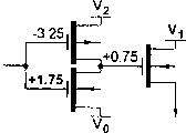
Can the logical zero input of following dissection on F210 or base-1 complementer circuit.With reference now to Figure 95 and F210,, or base-1 complementer circuit, for the circuit input V of logical zero
0(0V), 0 volt of input transfer is to the grid of all IGFET: top IGFET Q1, middle IGFET branch and bottom IGFET Q4, middle IGFET branch has its first and second medial fascicle IGFET Q2, Q3.
Bottom IGFET Q4 is a N channel enhancement IGFET, and it has absolute threshold (0 volt of source voltage (V of one 3.25 volts
0) add 3.25 volts of gate voltage (V
GS (TH))).Because bottom IGFETQ4 is a N channel enhancement IGFET, so only to the grid step voltage on its absolute threshold, source voltage just is sent to drain electrode.For the grid of bottom IGFET Q4, the circuit of logical zero input V
0(0V) under its absolute threshold of 3.25 volts, and bottom IGFET Q4 does not pass to its drain electrode and circuit output to the voltage of its source electrode.Circuit input V for logical zero
0(0V), not transfer circuit output of bottom IGFET.
There are two IGFET Q2, Q3 in centre IGFET branch, and they are connected in series in logical one, V
1(2.5V) between the output of source voltage and circuit.Medial fascicle IGFET Q2, Q3 both are connected with circuit input grid.Source electrode and the logical one of the first medial fascicle IGFET Q2, V
1(2.5V) source voltage connects.The drain electrode of the first medial fascicle IGFET Q2 is connected with the source electrode of the second medial fascicle IGFETQ3.The drain electrode of the second medial fascicle IGFET Q3 is connected with circuit output.
The first medial fascicle IGFET Q2 is a P channel depletion type IGFET, and it has absolute threshold (2.50 volts of source voltage (V of one 4.25 volts
1) add 1.75 volts of gate voltage (V
GS (TH))).Because the first medial fascicle IGFET Q2 is a P-channel enhancement type IGFET, so only to the gate voltage under its absolute threshold, source voltage just is sent to drain electrode.For the grid of the first medial fascicle IGFET Q2, the circuit of logical zero input V
0(0V) under its absolute threshold of 4.25 volts, and the first medial fascicle IGFET Q2 does not pass to its drain electrode to the voltage of its source electrode.Circuit input V for logical zero
0(0V), the first medial fascicle IGFET Q2 is logical one, V
1(2.5V) pass to its drain electrode and source electrode of the second medial fascicle IGFET Q3.
The second medial fascicle IGFET Q3 is a N channel depletion type IGFET, and it has absolute threshold (2.50 volts of source voltage (V of 0.75 volt
1) add (1.75) volt gate voltage (V
GS (TH))).Logical one, V
1(2.5V) source voltage is applied to the second medial fascicle IGFET Q3 by the drain electrode of the first medial fascicle IGFET Q2.Because the second medial fascicle IGFET Q3 is a N channel depletion type IGFET, so only to the gate voltage on its absolute threshold, source voltage just is sent to drain electrode.For the grid of the second medial fascicle IGFET, the circuit of logical zero input V
0(0V) under its absolute threshold of 0.75 volt, and the second medial fascicle IGFET Q3 does not pass to its drain electrode and circuit output to the voltage of its source electrode.Circuit input V for logical zero
0(0V), not transfer circuit output of the second medial fascicle IGFET Q3.Circuit input V for logical zero
0(0V), not transfer circuit output of middle IGFET branch.
Top IGFET Q1 is a P-channel enhancement type IGFET, and it has absolute threshold (5 volts of source voltage (V of 1.75 volts
2) add (3.25) volt gate voltage (V
GS (TH))).Because top IGFETQ1 is a P-channel enhancement type IGFET, so only to the gate voltage under its absolute threshold, source voltage just is sent to drain electrode.For the grid of top IGFET Q1, the circuit of logical zero input V
0(0V) under its absolute threshold of 1.75 volts.Top IGFET Q1 is not the voltage of its source electrode (logic 2, V
2, 5V) be sent to its drain electrode and circuit output.Circuit output V for logical zero
0(0V), IGFET Q1 in top transmits the circuit output V of logic 2
2(5V).
By the above, as seen import V for the circuit of logical zero
0(0V), the F210 circuit responds, and transmits logic 2 output V
2(5V).Only there is top IGFET Q1 that its source voltage is sent to the output of circuit, provides its logic 2 outputs logical zero is input as circuit.The grid input voltage of top IGFETQ1 is under its absolute threshold, so top IGFET Q1 is its logic 2 source voltage V
2(5V) be sent to circuit output.
Centre IGFET branch is not sent to circuit output to signal voltage.The first medial fascicle IGFET Q2 is not its source voltage logical one, V
1(2.5V) be sent to its drain electrode, because the grid input voltage is under its absolute threshold.The second medial fascicle IGFET Q3 does not transmit its source voltage logical one, V from the drain electrode of the first medial fascicle IGFET Q2
1(2.5V), because the grid input voltage of the second medial fascicle IGFET Q3 under its absolute threshold.The second medial fascicle IGFET Q3 prevents logical one, V
1(2.5V) signal voltage is from the further transmission of the first medial fascicle IGFET.
Bottom IGFET Q4 is not sent to circuit output to signal voltage.Bottom IGFET Q4 is not its logical zero source voltage V
0(0V) be sent to its drain electrode and circuit output, because the circuit of logical zero input V
0(0V) under its absolute threshold of 3.25 volts.
For the logical zero input, the F210 circuit transmits logic 2 outputs.
The effect that the logical one of F210 or base-1 complementer circuit is imported is as follows.Circuit input V for logical one
1(2.5V), 2.50 volts input transfer is to the grid of all IGFET: top IGFET Q1, middle IGFET branch and bottom IGFET Q4, middle IGFET branch has its first and second medial fascicle IGFET Q2, Q3.
Bottom IGFET Q4 is a N channel enhancement IGFET, and it has absolute threshold (0 volt of source voltage (V of 3.25 volts
0) add 3.25 volts of gate voltage (V
GS (TH))).Because bottom IGFETQ4 is a N channel enhancement IGFET, so only to the gate voltage on its absolute threshold, source voltage just is sent to drain electrode.For the grid of bottom IGFET Q4, the circuit of logical one input V
1(2.5V) under its absolute threshold of 3.25 volts, and bottom IGFET Q4 is not sent to its drain electrode and circuit output to the voltage of its source electrode.Circuit input V for logical one
1(2.5V), not transfer circuit output of bottom IGFET Q4.
There are two IGFET Q2, Q3 in centre IGFET branch, and they are connected in series in logical one, V
1(2.5V) between the output of source voltage and circuit.Medial fascicle IGFET Q2, Q3 are connected with circuit input grid.Source electrode and the logical one of the first medial fascicle IGFET Q2, V
1(2.5V) source voltage connects.The drain electrode of the first medial fascicle IGFET Q2 is connected with the source electrode of the second medial fascicle IGFET Q3.The drain electrode of the second medial fascicle IGFET Q3 is connected with circuit output.
The first medial fascicle IGFET Q2 is a P channel depletion type IGFET, and it has absolute voltage (2.50 volts of source voltage (V of 4.25 volts
1) add 1.75 volts of gate voltage (V
GS (TH))).Because the first medial fascicle IGFET Q2 is a P channel depletion type IGFET, so only to the gate voltage under its absolute threshold, source voltage just is sent to drain electrode.For the drain electrode of the first medial fascicle IGFETQ2, the circuit of logical one input V
1(2.5V) under its absolute threshold of 4.25 volts, and the first medial fascicle IGFET does not pass to its drain electrode to the voltage of its source electrode.Circuit input V for logical one
1(2.5V), the first medial fascicle IGFET Q2 is logical one, V
1(2.5V) be sent to its drain electrode and source electrode of the second medial fascicle IGFET Q3.
The second medial fascicle IGFET Q3 is a N channel depletion type IGFET, and it has absolute voltage (2.50 volts of source voltage (V of 0.75 volt
1) add (1.75) volt gate voltage (V
GS (TH))).Logical one, V
1(2.5V) source voltage is applied to the second medial fascicle IGFET Q3 by the drain electrode of the first medial fascicle IGFET Q2.Because the second medial fascicle IGFET Q3 is a N channel depletion type IGFET, so only to the gate voltage on its absolute threshold, source voltage just is sent to drain electrode.For the grid of the second medial fascicle IGFET Q3, the circuit of logical one input V
1(2.5V) under its absolute threshold of 0.75 volt, and the second medial fascicle IGFET Q3 does not pass to its drain electrode and circuit output to the voltage of its source electrode.Circuit input V for logical one
1(2.5V), the second medial fascicle IGFET Q3 is logical one, V
1(2.5V) be sent to its drain electrode and circuit output.Circuit input V for logical one
1(2.5V), middle IGFET branch transmits the circuit output V of logical one
1(2.5V).
Top IGFET Q1 is a P-channel enhancement type IGFET, and it has absolute threshold (5 volts of source voltage (V of 1.75 volts
2) add (3.25) volt gate voltage (V
GS (TH))).Because top IGFETQ1 is a P-channel enhancement type IGFET, so only to the gate voltage under its absolute threshold, source voltage just is sent to drain electrode.For the grid of top IGFET Q1, the circuit of logical one input V
1(2.5V) on its absolute threshold of 1.75 volts.Top IGFET Q1 is not the voltage of its source electrode (logic 2, V
2, 5V) be sent to the output of drain electrode and circuit.Circuit output V for logical one
1(2.5V), IGFET Q1 in top does not transmit logical circuit output.
By the above, as seen import V for the circuit of logical one
1(2.5V), the F210 circuit responds, and transmits logical one output V
1(2.5V).Only there is middle IGFET branch that its source voltage is sent to the output of circuit, provides its logical one output logical one is input as circuit.The grid input voltage of middle IGFET branch is under the absolute threshold of the first medial fascicle IGFET Q2, and on the absolute threshold of the second medial fascicle IGFET Q3.Because two medial fascicle IGFET Q2, Q3 are sent to their source voltage their drain electrode, so medial fascicle is the source voltage V of its logical one
1(2.5V) be sent to circuit output.
Bottom IGFET Q4 is not sent to circuit output to signal voltage.Bottom IGFET Q4 is not the source voltage V of its logical zero
0(0V) be sent to its drain electrode and circuit output, because the circuit of logical one input V
1(2.5V) under its absolute threshold of 3.25 volts.
Top IGFET Q1 is not sent to circuit output to signal voltage.Top IGFET Q1 is not the source voltage V of its logic 2
2(5V) be sent to its drain electrode and circuit output, because the circuit of logical one input V
1(2.5V) on its absolute threshold of 1.75 volts.
For the logical one input, the F210 circuit transmits logical one output.
Logic 2 inputs to F210 base-1 complementer circuit are as follows.Circuit input V for logic 2
2(5V), 5 volts input transfer is to the grid of all IGFET: top IGFET Q1, middle IGFET branch and bottom IGFET Q4, middle IGFET branch has its first and second medial fascicle IGFET Q2, Q3.
Bottom IGFET Q4 is a N channel enhancement IGFET, and it has absolute threshold (0 volt of source voltage (V of 3.25 volts
0) add 3.25 volts of gate voltage (V
GS (TH))).Because bottom IGFETQ4 is a N channel enhancement IGFET, so only to the gate voltage on its absolute threshold, source voltage just is sent to drain electrode.For the grid of bottom IGFET Q4, the circuit of logic 2 input V
2(5V) on its absolute threshold of 3.25 volts, and bottom IGFET Q4 is sent to its drain electrode and circuit output to the voltage of its source electrode.Circuit input V for logic 2
2(5V), IGFET Q4 in bottom transmits the circuit output V of logical zero
0(0V).
Centre IGFET branch has two IGFET Q2, Q3, and they are connected in series in logical one, V
1(2.5V) between the output of source voltage and circuit.Medial fascicle IGFET Q2, Q3 both are connected with circuit input grid.Source electrode and the logical one of the first medial fascicle IGFET Q2, V
1(2.5V) source voltage connects.The drain electrode of the first medial fascicle IGFET Q2 is connected with the source electrode of the second medial fascicle IGFET Q3.The drain electrode of the second medial fascicle IGFET Q3 is connected with circuit output.
The first medial fascicle IGFET Q2 is a P channel depletion type IGFET, and it has absolute voltage (2.50 volts of source voltage (V of 4.25 volts
1) add 1.75 volts of gate voltage (V
GS (TH))).Because the first medial fascicle IGFET Q2 is a P channel depletion type IGFET, so only to the gate voltage under its absolute threshold, source voltage just is sent to drain electrode.For the drain electrode of the first medial fascicle IGFETQ2, the circuit of logic 2 input V
2(5V) on its absolute threshold of 4.25 volts, and the first medial fascicle IGFET Q2 does not pass to its drain electrode to the voltage of its source electrode.Circuit input V for logic 2
2(5V), the first medial fascicle IGFET Q2 is logical one, V
1(2.5V) be sent to its drain electrode and source electrode of the second medial fascicle IGFET Q3.
The second medial fascicle IGFET Q3 is a N channel depletion type IGFET, and it has absolute threshold (2.50 volts of source voltage (V of 0.75 volt
1) add (1.75) volt gate voltage (V
GS (TH))).Because the grid input voltage of the first medial fascicle IGFET Q2 is on its absolute threshold, thus logical one, V
1(2.5V) source voltage does not have the drain electrode by the first medial fascicle IGFET Q2, is applied to the second medial fascicle IGFET Q3.Because the second medial fascicle IGFET Q3 is a N channel depletion type IGFET, so only to the gate voltage on its absolute threshold, source voltage just is sent to drain electrode.For the grid of the second medial fascicle IGFET Q3, the circuit of logic 2 input V
2(5V) on its absolute threshold of 0.75 volt, and the second medial fascicle IGFET Q3 will not pass to its drain electrode and circuit output to the voltage of its source electrode.Yet, because the second medial fascicle IGFETQ3 does not have source voltage, so no-voltage is sent to drain electrode and the circuit output of the second medial fascicle IGFET Q3.Circuit input V for logic 2
2(5V), not transfer circuit output of the second medial fascicle IGFET Q3.Circuit input V for logic 2
2(5V), not transfer circuit output of middle IGFET branch.
Top IGFET Q1 is a P-channel enhancement type IGFET, and it has absolute threshold (5 volts of source voltage (V of 1.75 volts
2) add (3.25) volt gate voltage (V
GS (TH))).Because top IGFETQ1 is a P-channel enhancement type IGFET, so only to the gate voltage under its absolute threshold, source voltage just is sent to drain electrode.For the grid of top IGFET Q1, the circuit of logic 2 input V
2(5V) on its absolute threshold of 1.75 volts.Top IGFET Q1 is not the voltage of its source electrode (logic 2, V
2, 5V) be sent to the output of drain electrode and circuit.Circuit input V for logic 2
2(5V), not transfer circuit output of top IGFET Q1.
By the above, as seen import V for the circuit of logic 2
2(5V), the F210 circuit responds, and transmits logical zero output V
0(0V).Only there is bottom IGFET Q4 that its source voltage is sent to the output of circuit, provides its logical zero output logic 2 is input as circuit.The grid input voltage of bottom IGFETQ4 is on its absolute threshold, and therefore bottom IGFET Q4 is the source voltage V of its logical zero
0(0V) be sent to circuit output.
Centre IGFET branch is not sent to circuit output to signal voltage.Because the grid input voltage is on its absolute threshold, so the first medial fascicle IGFET Q2 is not its source voltage logical one, V
1(2.5V) be sent to its drain electrode.Because the grid input voltage of the second medial fascicle IGFET Q3 is under its absolute threshold, so the second medial fascicle IGFET Q3 will be sent to its drain electrode to its source voltage.Yet, owing to the source electrode no-voltage of IGFET Q3 in the middle of second, so to not influence of circuit output.The first medial fascicle IGFET Q2 has prevented logical one, V
1(2.5V) signal voltage is sent to the second medial fascicle IGFET Q3 and circuit output.
Top IGFET Q1 is not sent to circuit output to signal voltage.Top IGFET Q1 is not the source voltage V of its logic 2
2(5V) be sent to its drain electrode and circuit output, because the circuit of logic 2 input V
2(5V) on its absolute threshold of 1.75 volts.
For logic 2 inputs, the F210 circuit transmits logical zero output.
In the F210 circuit, for logical zero circuit input V
0(0V), IGFET Q1 in top transmits logic 2 circuit output V
2(5V); For logical one circuit input V
1(2.5V), the middle IGFET transmission logical one circuit output V of branch that has its first and second IGFET Q2, Q3
1(2.5V); And for logic 2 circuit input V
2(5V), IGFET Q4 in bottom transmits logical zero circuit output V
0(0V).These three IGFET branches only make response to a value of logic input separately, transfer circuit output.
The above analysis to F210 ternary OPF can guide and be any SUS-LOC circuit.By analyzing input voltage, source voltage and gate threshold voltage (V
GS (TH)), can determine the response characteristic of any SUS-LOC OPF circuit.This process also can expand to the multidigit function.
The multidigit function
Here narrate ternary multidigit function (MPF), binary system and quinary (base 5) are done some reference.The MPF of any base can realize with the SUS-LOC structure.For example, table N shows " two bit functions " of base 2.Two very how possible bit functions are arranged.For base 2, the number of two possible bit functions is ten six (16 or 2
4).For base 2 to 9, number is greater than 10
77Own for base 10, the number of two bit functions is 10
100
A MPF comes down to the combination of two or more bit functions of same base.Though single multidigit function possibility, the combination of the base within single multidigit function is comparatively advanced and complicated.Each input of a MPF is the input that is used to form one or more bit functions of MPF.The branch of each bit function is arranged to similar branch series, parallel or the connection in series-parallel conduction to other OPF, to form compound branch.Similar branch is those for given input logic level combination, the branch that output is connected with identity logic level power source.
Each MPF, no matter its figure place and radix what, all respond it by the input that the combination of all possible input logic level circulates, produce unique output sequence.The ternary logic system comprises 19,683 (3
9) individual two possible bit functions, each is by 9 input combinations.This is 2.25 times of input state number of binary system two bit functions.Yet, be not that all possible MPF of given base and figure place is useful.The collection of MPF comprises r continuous function and can be reduced to the function of less bits, maybe can be reduced to the function of low base, or those functions that either way exist.When base greater than 2 the time, might simplify the figure place and/or the radix of function.
Following table N shows 16 two bit functions of binary system.
Table N
| # | B=1,A=1 | B=1,A=0 | B=0,A=1 | B=0,A=0 | Name or descriptor |
| 0 | 0 | 0 | 0 | 0 | Continuously |
| 1 | 0 | 0 | 0 | 1 | " NOR " door |
| 2 | 0 | 0 | 1 | 0 | " AND " door with reverse input " B " |
| 3 | 0 | 0 | 1 | 1 | Be reduced to the inverter of input " B " |
| 4 | 0 | 1 | 0 | 0 | " AND " door with oppositely " A " input |
| 5 | 0 | 1 | 0 | 1 | Be reduced to the inverter of input " A " |
| 6 | 0 | 1 | 1 | 0 | Different " OR " door (XOR) |
| 7 | 0 | 1 | 1 | 1 | " NAND " door |
| 8 | 1 | 0 | 0 | 0 | " AND " door |
| 9 | 1 | 0 | 0 | 1 | " XOR " with reverse output |
| 10 | 1 | 0 | 1 | 0 | Be reduced to the buffer of input " A " |
| 11 | 1 | 0 | 1 | 1 | " OR " door with oppositely " B " input |
| 12 | 1 | 1 | 0 | 0 | Be reduced to the buffer of input " B " |
| 13 | 1 | 1 | 0 | 1 | " OR " door with oppositely " A " input |
| 14 | 1 | 1 | 1 | 0 | " OR " door |
| 15 | 1 | 1 | 1 | 1 | Continuously |
As show shown in the N, some function has familiar name, for example " different OR " and " NAND " door.As previously mentioned, r continuous function arranged.For the binary system situation, there are 2: No. 0 and No. 15.Has the function that can be reduced to less bits: No. 3, No. 5, No. 10 and No. 12.If make mark reverse, image feature is expressed as No. 2 (it be 4 mirror image) and 11 (it be 13 mirror image).For the MPF of any base and any figure place, situation also is like this.Use binary system in this case, the useful mode of a kind of expression by the characteristic that all MPF shared of any base is provided.
Below the exploratory method of MPF is discerned in narration with text and diagram.These methods are tentative, because along with the further developing of r value logic and SUS-LOC structure, various improvement and/or variation take place in expection.
When text ground during with reference to MPF, the abbreviation name of function (the supposition function is named) is write subscript with the base of expectation function.For example, ternary CGOR is called " CGOR
3", and quinary GOR is called " GOR
5".If omitted the subscript base, be assumed to base 3 so here.Binary functions is used the consistent name of they current and fixed conventions.
A system of selection of identification is to function numbering, and for the numbering of identification and classification function of use.Numbering can be by carrying out the power of each outgoing position allocation base in the Karnaugh map of function.Function with mixed base is possible.Table O shows for ternary logic the distribution of 3 power.
Table O
GAND
3Karnaugh map (Figure 134) represent with the power of this numerical system employed 3 among the P at table.The value of each power to 3 adds up to, and obtains GAND
3Coding, it is ternary two bit function sign indicating numbers 113.
Table P
The basic symbol of MPF is shown in Figure 112.Figure 113 has represented the symbol of GAND door, and it is provided with " r " in the position that the base for function keeps.GOR
3The symbol of door is shown in Figure 114.When omitting the subscript base, be assumed to base 3 so.Binary functions is used their current symbols with note or caption, and the desired SUS-LOC of the suitable interface of deixis realizes.Other r value logical symbols will be along with based on the development of the r value logic of SUS-LOC structure and development simultaneously.
As previously mentioned, 19,683 possible ternary two bit functions are arranged, and 19,632 is useful.Yet, when the exchange input marking, some repetition and/or mirror image.
In 19,632 ternary two bit functions, only narrate here several, with operation that SUS-LOC is provided and practical relevant example.Some has binary class seemingly in the door, and some no simple gate binary system is separated or be similar.Here narration and known binary system NAND, NOR and the similar door of XOR.Also narrate the quinary logic function, the logic function that can synthesize any base with main expression.Use base 5 to have some advantage.And the design parameter of ternary and quinary circuit is shown in table Q, has the parameter according to the binary functions of standard CMOS parametric representation.
Table Q
| Logic system | LSV | OP | V
0 | V
1 | V
2 | V
3 | V
4 |
| Ternary | 2.5V | 70% | 0.0V | 2.5V | 5.0V | | |
| Quinary | 2.0V | 70% | 0.0V | 2.0V | 4.0V | 6.0V | 8.0V |
Because MPF comes down to the combination of two or more bit functions of same base,, can represent to form the combination of the OPF of MPF by this exemplary circuit so CGOR and CGAND door provide exemplary circuit.At Figure 115 to Figure 117, Figure 118 to Figure 120, among Figure 121 to Figure 123 and Figure 124 to Figure 126, represented CGOR respectively
3, CGAND
3, CGOR
5And CGAND
5Schematic diagram, symbol and Karnaugh map.And mirage is represented to expand three and is advanced the desired element of value door.The expansion of corresponding quinary door realizes with similar approach.
CGOR
3And CGAND
3Door is made of base 3 bases-1 of each input item complementer, and the similar branch of each complementer is series, parallel or connection in series-parallel setting as required, to realize the logic function of CGOR or CGAND.Figure 115 and Figure 118 represent that a complementer is made of Q2, Q4, Q6 and Q7, and another complementer is made of Q1, Q3, Q5 and Q8.
CGOR
rWith CGAND
rBetween be not both: which compound branch (being made of terminal branch) is connected in series, and which is connected in parallel; And for the formed compound branch of medial fascicle, which kind of channel type forms its series connection part, and which kind of channel type forms its part in parallel.
In Figure 115, the similar branch of arranged in series regards the formed compound branch of the terminal branch of being made up of Q1 and Q2 as.The similar branch that is arranged in parallel regards the formed compound branch of the terminal branch of being made up of Q7 and Q8 as.The similar branch of connecting/being arranged in parallel regards as by the formed compound branch of medial fascicle, and these medial fascicles are made up of with Q5 in parallel and Q6 arranged in series series connection Q3 and Q4.
Figure 115 and Figure 118 have relatively disclosed CGOR
3With CGAND
3Between difference.CGAND
3Schematic diagram represent in parallel and series terminal branch is inverted, and the inversion of the channel type within the series connection/compound branch in parallel.
CGOR about Figure 115
3Circuit should notice that when input A was 0, output C followed the complement code of input B.Be further noted that when input A is 2 to any input B, output C is 0.Because input A and B can exchange, so also be true (replace input A with input B, vice versa) on the contrary.
The circuit element of CGOR circuit is the mixing of depletion type FET and enhancement mode FET.One group of N channel enhancement FET plays intermediation, V
0Be sent to output C, with control V
0Output.The P channel depletion type FET of one group of combination and N channel depletion type FET play intermediation, V
1Be sent to output C, with control V
1Output.One group of P-channel enhancement type FET plays intermediation, V
2Be sent to output C, with control V
2Output.These groups FET is as the identification input, so that control and produce the suitable output of CGOR circuit.
Shown in Figure 115, V
0Be connected with output C by the N channel enhancement FET that is connected in parallel.Each input there is the N channel enhancement FET of a correspondence, and the grid connection of signal of each input and corresponding FET.FET is connected in parallel, so that only there is one must conduct among the FET, so that V
0Signal be sent to output C.All V
0The V of FET
GS onBe 3.25 volts (producing 3.25 volts absolute gate threshold voltage), so that make V
0Signal be sent to output C, input A or B must be at V
2When input A or B are 2, like this corresponding to the true tabular value of output C.When input A and input B both be logic level 1 or under the time, V
0Signal can't help Q7 or Q8 and be sent to output C.
The two sets intersect circuit plays intermediation, V
1Be sent to output C.First circuit structure is one group of P channel depletion type FET, with 1.75 volts gate threshold voltage V
GS off(producing 4.25 volts absolute gate threshold voltage) is connected in series.The second circuit structure is one group of N channel depletion type FET, with-1.75 volts gate threshold voltage V
GS off(producing 0.75 volt absolute gate threshold voltage) is connected in parallel.Two circuit structures are connected in series mutually, so that the output of first circuit structure is before reaching output C, and must be by the second circuit structure.The FET Q4 of two circuit structures is connected with input A grid with Q5.FET Q3 is connected with input B grid with Q6.For the CGOR circuit with additional input, the input grid that the corresponding FET of two circuit structures is corresponding with them connects.
As input A or input B when being logic level 2 (or on logic level 1), first circuit structure with its P channel depletion type FET Q3, Q4 is as preventing V
1Be sent to output C.Because Q3, Q4 are connected in series, and prevent V so the input of any logic level 2 on any FET of first circuit structure all is used as
1Be sent to output C.Only when input A and B all be logic level 1 or under the time, the FET of first circuit structure is just V
1Be transmitted to the second circuit structure.
When input A or input B be logic level 1 or on the time, the second circuit structure with its N channel depletion type FET Q5, Q6 is as allowing V
1Be sent to output C.Because FET is connected in parallel, thus from any input (A, B, n...) in logic level 1 or on any input, all allow from a P channel depletion type circuit structure V
1Be sent to output C.
The second circuit structure has one group of N channel depletion type FET Q5, Q6, and they are connected in parallel with-1.75 volts threshold voltage (producing 0.75 volt absolute gate threshold voltage).If the input A or the input B be logical one or on, at least one FET of second circuit structure will place its conduction pattern, so as the output of first circuit structure be sent to output C.If input A and input B both are logic level 0, do not have FET to place its conduction pattern in the second circuit structure, and the first circuit structure no-output is sent to output C.Like this, be logic level 0 for input A and B both, the second circuit structure has prevented V
1Be sent to output C.So for input A and B both in logic level 0, the response of the circuit of CGOR circuit only by with V
2Related series circuit transmission.
Only when input A and B both be logic level 1 or under the time, FET Q3, the Q4 ability of first circuit structure is V
1Be transmitted to the second circuit structure.When input A and B both are logic level 0, with V
1First circuit structure that connects will be V
1Be transmitted to the P channel depletion type FET Q3 that is connected in series, the terminal of Q4.Though for importing A and B both 0, circuit should only exported C with V
2Respond, prevented, abnormal conditions will occur, wherein V if still keep
1And V
2The both will be sent to output C.For importing A and B both 0, in order to prevent V
1Be sent to output C, the second circuit structure and first circuit structure of N channel depletion type FET Q5 in parallel, Q6 are connected in series.
When input A is V with input B both
0The time, the CGOR circuit is output as V
2V
2Source signal is connected with output C by P-channel enhancement type FET Q1, Q2, and FET Q1, Q2 transmit V together
2The circuit response.Each input there is the P-channel enhancement type FET of a correspondence, and the grid connection of signal of each input and corresponding FET.FET is connected in series mutually, so that for V
2Source voltage is sent to output C, and all FET must conduct.The V of all FET
GS onBe-3.25 volts (producing 1.75 volts absolute gate threshold voltage), so that for V
2Signal is sent to output C, and input A and B both are necessary for V
0This situation is exported the true tabular value of C corresponding to when input A and B both be logic level 0.When input A or B are on logic level 0, no V
2Signal is sent to output C.
The CGOR circuit can expand to handles any input number.Such possibility the 3rd input be expressed as input " n ", and the adjunct circuit of this requirement is represented with mirage in Figure 115.This additional requirement circuit meets the overall circuit of CGOR circuit, to the circuitous pattern that two input CGOR circuit are proposed, for example the above input circuitous pattern that A and B proposed is expanded.
For desired each additional input of CGOR circuit, requiring has an additional FET to each CGOR circuit minor structure.In order to transmit V
0Output, additional N channel depletion type FET with corresponding to input A and B to transmit V
0The FET of output is connected in parallel.In order to transmit V
1Output requires an additional classes like FET to first series circuit configuration and the second parallel circuits structure both.Other FET of the additional P channel depletion type FET and first circuit structure are connected in series, and other FET of additional N channel depletion type FET and second circuit structure are connected in parallel.In order to transmit V
2Output, additional P-channel enhancement type FET with corresponding to input A and B to transmit V
2The FET of output is connected in series.The grid input of additional FET connects with corresponding additional input.Even for additional more inputs, the response characteristic of CGOR circuit also keep the true tabular value as table C general shown in.
Should notice how similar with the F210 base-1 complementer circuit (Figure 95) of a bit function circuit CGOR circuit is.By removing the circuit related with importing B, the CGOR circuit becomes F210 base-1 complementer circuit.And, should note the connection in series-parallel character of circuit.V
0That part of of CGOR circuit that is sent to output C is in parallel, transmits V
2Part be series connection, and transmit V
1Part have a series connection part of connecting with part in parallel.
Following table is represented for different A and B input, the response of respective transistors Qn.Those keep blank table input item indication input and do not control this transistor Qn.
| | Q1 | Q2 | Q3 | Q4 | Q5 | Q6 | Q7 | Q8 |
| A | 0 | | Connect | | Connect | | Disconnect | Disconnect | | |
| 1 | Disconnect | Connect | Connect | Disconnect | |
| 2 | Disconnect | Disconnect | Connect | Connect |
| B |
| | 0 | Connect | | Connect | | Disconnect | | | Disconnect | |
| 1 | Disconnect | Connect | Connect | Disconnect | |
| 2 | Disconnect | Disconnect | Connect | Connect |
CGAND for Figure 118
3Circuit should notice that when input A was 0, output C always was 2.Be further noted that when input A was 2, output C followed the complement code of input B.Because input A and B are interchangeable, also be true (B replaces A with input, and vice versa) on the contrary.
In general, the CGAND circuit aspect response and the structure two is being replenishing of CGOR circuit.Use FET in parallel at the CGOR circuit, with V
0Be delivered to the occasion of output C, the CGAND circuit uses series connection FET.Use series connection P channel depletion type FET and N channel depletion type FET in parallel at the CGOR circuit, with V
1Be delivered to the occasion of output C, the CGAND circuit uses series connection N channel depletion type FET and P channel depletion type FET in parallel.Use series connection FET at the CGOR circuit, with V
2Be delivered to the occasion of output C, the CGAND circuit uses FET in parallel.By the circuit diagram of inspection Figure 115 and Figure 118, and the truth table of Figure 117 and Figure 120, other characteristics of as seen replenishing the CGAND circuit of CGOR circuit.
As the CGOR circuit, the circuit element of CGAND circuit is the mixing of depletion type FET and enhancement mode FTE.One group of N channel enhancement FET plays intermediation, V
0Be sent to output C, with control V
0Output.The N channel depletion type FET of one group of combination and P channel depletion type FET play intermediation, V
1Be sent to output C, with control V
1Output.One group of P-channel enhancement type FET plays intermediation, V
2Be sent to output C, with control V
2Output.These groups FET is as the identification input, so that control and produce the suitable output of CGAND circuit.
Shown in Figure 118, V
0Be connected with output C by N channel enhancement FET Q7, the Q8 that is connected in series.When all are input as V
2The time, the CGAND circuit is output as V
0Each input there is the N channel enhancement FET of a correspondence, and the grid connection of signal of each input and corresponding FET.Each FET and V
0V is transmitted in the FET association that is connected in series in addition of output circuit group
0The circuit response.FET is connected in series, so that all FET must conduct, so that V
0Signal be sent to output C.The V of all FET
GS onBe 3.25 volts (producing 3.25 volts absolute gate threshold voltage), so that make V
0Signal be sent to output C, all input A and B boths must be at V
2When input A is 2 with input B both, like this corresponding to the true value tabular value of exporting C.When input A or input B are under the logic level 2 time, no V
0Signal is sent to output C.
The two sets intersect circuit structure plays intermediation, V
1Be sent to output C.First circuit structure is one group of N channel depletion type FET Q3, Q4, with-1.75 volts gate threshold voltage V
GS off(producing 0.75 volt absolute gate threshold voltage) is connected in series.The second circuit structure is one group of P channel depletion type FET Q5, Q6, with+1.75 volts grid threshold value V
GS off(producing 4.25 volts absolute gate threshold voltage) is connected in parallel.Two circuit structures are connected in series mutually, so that the output of first series circuit configuration is before reaching output C, and must be by the second parallel circuits structure.Two both FET of circuit structure are connected with input A grid.Two both FET of circuit structure are connected with input B grid.
As input A or input B when being logic level 0 (or under logic level 1), first circuit structure with its N channel depletion type FET Q3, Q4 is as preventing V
1Be sent to output C.Because FET Q3, Q4 are connected in series, so any logic level 0 input on any FET of first circuit structure is as preventing V
1Be sent to output C.Only when input A and B both be logic level 1 or on the time, FET Q3, the Q4 ability of first circuit structure is V
1Be transmitted to the second circuit structure.
When input A or input B be logic level 1 or under the time, the second circuit structure with its P channel depletion type FET Q5, Q6 is as allowing V
1Be sent to output C.Because FET is connected in parallel, thus from any input (A, B, n...) in logic level 1 or on any input, allow from a N channel depletion type circuit structure V
1Be sent to output C.
The 2nd V
1Circuit structure has one group of P channel depletion type FET Q5, Q6, the threshold voltage V of they and 1.75 volts
GS off(producing 4.25 volts absolute gate threshold voltage) is connected in parallel.If the input A or the input B be logical one or under, at least one FET of second circuit structure will place its conduction pattern, so as the output of first circuit structure be sent to output C.If input A and input B both are logic level 2, do not have FET to place its conduction pattern in the second circuit structure, and the first circuit structure no-output is sent to output C.Like this, be logic level 2 for input A and B both, the second circuit structure has prevented V
1Be sent to output C.So for input A and B both in logic level 2, the response of the circuit of CGAND circuit only by with V
0Related series circuit transmission.
When input A and B both are logic level 2, with V
1First circuit structure that connects will be V
1Be transmitted to the N channel depletion type FET Q3 that is connected in series, the terminal of Q4.Though for importing A and B both 2, circuit should only exported C with V
0Respond, prevented, abnormal conditions will occur, wherein V if still keep
1And V
2The both will be sent to output C.For importing A and B both 2, in order to prevent V
1Be sent to output C, the second circuit structure and first circuit structure of P channel depletion type FET Q5 in parallel, Q6 are connected in series.
When importing A or importing B is V
0The time, the CGAND circuit is output as V
2V
2Be connected with output C by P-channel enhancement type FET Q1, the Q2 that is connected in parallel, and for V
2Be sent to output C, only have one must place conduction pattern by its grid input.Each input there is the P-channel enhancement type FET of a correspondence, and the grid connection of signal of each input and corresponding FET.The V of all FET
GS onBe-3.25 volts (producing 1.75 volts absolute gate threshold voltage), so that for V
2Signal is sent to output C, and arbitrary input A or B are necessary for V
0This situation is corresponding to when input A or B are logic level 0, the true tabular value of output C.When input A and B both are on logic level 0, no V
2Signal is sent to output C.
The CGAND circuit can expand to handles any input number.Such possibility the 3rd input be expressed as input " n ", has the additional requirement circuit shown in the mirage among Figure 118.This additional requirement circuit meets the overall circuit of CGAND circuit, to the circuitous pattern that two input CGAND circuit are proposed, for example the above input circuitous pattern that A and B proposed is expanded.
For desired each additional input of CGAND circuit, requiring has an additional FET to each CGAND circuit minor structure.In order to transmit V
0Output, additional N channel enhancement FET with corresponding to input A and B to transmit V
0The FET of output is connected in series.In order to transmit V
1Output requires an additional classes like FET to first series circuit configuration and the second parallel circuits structure both.Other FET of the additional N channel depletion type FET and first circuit structure are connected in series, and other FET of additional P channel depletion type FET and second circuit structure are connected in parallel.In order to transmit V
2Output, an additional P-channel enhancement type FET and the original FET that is connected in parallel are connected in parallel, and are connected with output C, and the source electrode of this FET is at V
2, and the input corresponding with it of its grid connects.Even for additional more inputs, the response characteristic of CGAND also keeps as identical like that shown in the true tabular value of Figure 120 is general.
Should notice how similar with the F210 base-1 complementer circuit (Figure 95) of a bit function circuit CGAND circuit is.By removing the circuit related with importing B, the CGAND circuit becomes F210 base-1 complementer circuit.And, should note the connection in series-parallel character of circuit.V
0That part of of CGAND circuit that is sent to output C is series connection, transmits V
2Part be in parallel, and transmit V
1Part have a series connection part of connecting with part in parallel.In the CGOR circuit, there is similarity at the CGAND circuit.Check two circuit diagrams (Figure 118 and Figure 115), represented the difference of configuration aspects, it causes the different operating characteristic of two circuit.
Following table is represented for different A and B input, the response of respective transistors Qn.Those keep blank table input item indication input and do not control this transistor Qn.
| | Q1 | Q2 | Q3 | Q4 | Q5 | Q6 | Q7 | Q8 |
| A | 0 | | Connect | | Disconnect | | Connect | Disconnect | | |
| 1 | Disconnect | Connect | Connect | Disconnect | |
| 2 | Disconnect | Connect | Disconnect | Connect |
| B |
| | 0 | Connect | | Disconnect | | Connect | | | Disconnect | |
| 1 | Disconnect | Connect | Connect | Disconnect | |
| 2 | Disconnect | Connect | Disconnect | Connect |
Non-complement code logical circuit also can be realized by SUS-LOC.Because the mode of operation of present available switch is as implied above, considers non-reverse sequence, the output voltage of single-level circuit must move with the relative direction of the input voltage of circuit.Therefore the basic single-stage function of MPF produces complement code or conversion output, so that avoid unusual path.In order to obtain a logic function, its output is not the complement code or the reverse sequence of its input, is necessary additional base-1 complementer or an other bit function.For the complement code that produces the input that is not function or reverse logic level, this is the situation of most of MPF.
This quality of SUS-LOG does not depend on base, and owing to switching manipulation causes.If such switch is not vulnerable to reverse bias, can omits and prevent so back-biased additional OPF.In addition, the suitable planning and the design of this inherent characteristics of SUS-LOC logic circuit structure indication combinational circuit are necessary, to guarantee the optimal design that has smallest elements, lower-wattage requirement and broadcast time of delay than short pass.
One example of non-complement code logic be Figure 127 and Figure 128 binary system NAND shown in respectively with the CMOS realization of AND door between different.Notice that the AND door is actually the NAND door that is added with inverter.
In order to form non-complement code or non-conversion logic function, simply basic logic functions is added base-1 complementer or another suitably basic OPF, as a preceding adjuster or post regulator.To produce the output sequence of wishing like this.GOR shown in Figure 129 to Figure 131 and Figure 132 to Figure 134 difference
3And GAND
3Realize by this back adjusting method.In these circuit, to basic GOR
3And GAND
3The output of door is base-1 complementer in addition.
Extra level
To the SUS-LOC circuit add the process of extra level and as a result circuit provide the structure of SUS-LOC and seeing clearly of design.
Figure 135 represents that the SUS-LOC of two ternary ∑ doors realizes.Item SUS-MOS refers to the embodiment of SUS-LOC, and its uses the unidirectional FET with dedicated source voltage.Those FET that for example are used for SUS-LOC are for P raceway groove and N channel fet, obtain their source respectively from corrigendum or negative voltage.
Figure 136 to Figure 144 represents the ∑ door, in nine combinations of input logic level each, represents to expect path with thick line respectively, and represents unusual path with dotted line.And Figure 136 to Figure 144 represents Karnaugh map, and mirage is unselected input and output positions.In addition, all unusual paths are shown in table R.
Table R
The unusual path of SUS-LOC ∑
| Figure # | Input A B | Output | The path of selecting or wishing | Unusual path (B#) by branch number |
| 1 | 0 | 0 | 0 | 9 | 1,2,3,5,6 |
| 2 | 1 | 0 | 1 | 5 | 1,2,9 |
| 3 | 2 | 0 | 2 | 2 | 5,9 |
| 4 | 0 | 1 | 1 | 6 | 1,3,9 |
| 5 | 1 | 1 | 2 | 1 | 5,6,9 |
| 6 | 2 | 1 | 0 | 8 | 4 |
| 7 | 0 | 2 | 2 | 3 | 6,9 |
| 8 | 1 | 2 | 0 | 7 | 3,4 |
| 9 | 2 | 2 | 1 | 4 | 7,8 |
Because the SUS-LOC circuit is not considered the source electrode of FET and drain electrode and is determined by size that places the voltage on them or polarity, so if with the actual realization of present available FET, undesirable conduction (or unusual path) takes place then.For the P channel fet, the source electrode is two corrigendums in the electrode; For the N channel fet, source electrode is more negative.Therefore, output voltage or logic level can exchange source electrode and the drain electrode of the FET that is used to form branch.When SUS-LOC forms a kind of fabulous device, when utilizing it to realize multi valued logic, must solve in another way obviously lacking of dedicated source FET.The following utilization shown in the extra level, SUS-LOC provides such mode.
If use present available FET in SUS-MOS designs, when generation source/drain electrode exchanged, input logic level may be enough not big or small, conducts to prevent unselected branch, and produce unusual path.Figure 136 represents that branch 2 is unusual path, and is used for the example of following explanation source/leakage exchange.
At A=0, under the input logic level of B=0, the branch of selection is a branch 9, and it is logical zero, V
0, zero volt is transmitted to output, shown in Figure 136 thick line.Because branch 2 also is connected with output, so the drain electrode that the voltage that is conducted by branch 9 places a P-channel enhancement type transistor QB.At gate voltage is subzero, because QA plays one the source electrode of QB and V
2, so 5 volts of very large resistor effects that connect are QB biasing conduction.So QB from output V
0Be transmitted to QA.
Because QA is the N channel device, and by the voltage (V of QB conduction
0) compare V
2Supply voltage is more negative, so the source electrode of QA is the electrode that is connected with QB now.Under " newly " source voltage of 0 volt, the input of QA or gate voltage (A=0) are enough not low, to disconnect QA, because V
0(A=0) not the V of QB
0Under " source "-1.75V.Under source/leakage exchange of QA, branch 2 is V
2Be transmitted to output.Under branch 9 and 2 boths of branch conduction, from V
2To V
0By the FET of branch 2 and 9, very high electric current is arranged.This unusual path also causes V
2-V
0/ 2 wrong output voltage.
Equally, branch's 3,5 and 6 following generation paths.At A=0, under the B=0 input, branch 9 is V
0All branches (comprising branch 3,5 and 6) that are sent to output and are connected with output.
For branch 3, V
0Output is sent to the drain electrode of QD, and QD is a N channel depletion type FET with grid threshold value of-1.75 volts.Because it is a N channel fet, so obtain its source from the more negative voltage that places its electrode (those are at the electrode of source electrode and drain electrode effect under precondition).Because V
0Less than V
2So it becomes the source of QD, and because B=0 (V
0) not V
0Under 1.75 volts, so QD opens and conducts.
For QC, on the P-channel enhancement type FET of QC (gate threshold voltage with-3.25 volts), QC is opened in the input of A=0, so that it is V
2Be transmitted to QD.When A=0 and B=0, because QC and QD both open, so from the V of branch 3
2The source is to the V of branch 9
0There is a unusual path in the source.
For branch 5, V
0Output is sent to QG, and QG is a P-channel enhancement type FET with gate threshold voltage of-0.75 volt.Because QG is a P channel fet, it obtains its source from the more positive voltage that acts on its non-input/non-gate electrode.Because the voltage on the opposite side of QG is V
1(directly conduction or the high resistance under the FET condition of closing by QE and/or QF) is so QG is from V
1Obtain its source voltage.Because B=0 (V
0) be V
1Under-0.75 volt, so work as A=0, during B=0, QG opens and V
0Conduction QF.
QF is a N channel depletion type FET with-1.75 volts of gate threshold voltages.It is from V
1Or V
0In obtain the smaller, be V under this situation
0, as the source of its N channel fet.Because QF obtains its source V
0So, the input (V of A=0
0) not V
0Under 1.75 volts.Therefore, QF opens and conducts to drain electrode from its source electrode.
QE is a P channel depletion type FET with 1.75 volts of gate threshold voltages.Because QE is a P channel fet, so it is from V
1Or V
0In obtain the greater, be V under this situation
0, as its source.Because A=0 (V
0) not greater than V
11.75 volts.So QE opens also V
1Be transmitted to drain electrode from its source electrode.
Because all three FET (QE, QF and QG) open, so the voltage source V of branch 5
1Be transmitted to output, simultaneously the source voltage (V of branch 9
0) also pass to output.As narrating similarly for branch 2, a unusual path with high electric current and wrong output voltage appears.
About branch 6, work as A=0, during B=0, analogue takes place.QJ is a P channel depletion type FET with gate threshold voltage of 1.75 volts.Because QJ is a P channel fet, so its arbitrary corrigendum from its non-input/non-gate electrode obtains its source.Though QH and QI can play very big resistor, as the V in the source of branch 6
1On act in the QJ electrode one, the V of branch 9
0Output action is on another.So QJ obtains V
1And V
0Middle corrigendum person is V under this situation
1, as its source.The input of B=0 on QJ is not V
1On 1.75 volts, and QJ connects, thus V
0Conduct back QI.
QI is a N channel depletion type FET with grid threshold value of-1.75 volts.V
1Apply in its non-input electrode, and V
0(passing through QJ) is applied on another electrode.Because QI is the N channel fet, so it gets V
1And V
0Middle corrigendum person is V under this situation
0, as its source.Because the input of the B=0 on the QI is not V
0Under 1.75 volts, so QI opens and V
0Pass to QH.
QH is a P-channel enhancement type FET with grid threshold value of 0.75 volt.Owing to be a P channel fet, so it is from V
1Or V
0In get corrigendum person, be V under this situation
1, as its source.Because the input of A=0 is less than V
10.75 volt, so QH connect, V
1Be sent to (by QI and QJ) output, have the V of branch 9 simultaneously
0 Output.As branch 2, occur one and have the corresponding high electric current and the unusual path of wrong output voltage.
As implied above, unusual path can appear in the SUS-LOC circuit, these SUS-LOC circuit are not considered the characteristic of N and P channel fet, with get respectively more negative on the electrode that is applied to them or more positive voltage as their source.Along with the development of unidirectional FET, the SUS-MOS embodiment of SUS-LOC thinks the very useful and advantageous embodiments of SUS-LOC.Yet about this point, the obvious unavailability of such dedicated source (or unidirectional) FET requires the transistor or the switch that are used for the SUS-LOC circuit are made adaptation.Figure 138 to Figure 144 represents relevant desired output and unusual path and the relevant promise figure value of card.These figure think enough from illustrative, so that when estimating the FET conduction, above-mentioned evaluation procedure can be applicable to these circuit structures.
Press the same manner, as seen in Figure 136 to Figure 144 and Biao R, for a combination of input logic level, all nine branches become a unusual path at least.Because unusual path causes very high electric current and unsuitable output logic level,, take place to prevent unusual path so must take measures.In the SIGMA circuit, can prevent the method and the design of so unusual path, be applicable to all SUS-LOC circuit.
In order to prevent that unusual path from taking place, require an additional single-stage OPF and/or transistor to replace, suitably switch on and off to guarantee that each of each branch is transistorized.This can finish by replacing branch's transistor with two transistor OPF, makes its output drive the suitably transistorized grid of conduction.
The transistorized absolute threshold voltage of the branch that is replaced is relevant with the supply voltage that it conducts.The gate threshold voltage V that is not both described FET between absolute threshold voltage and power supply or the source voltage
GS (TH), add gate threshold voltage because absolute threshold voltage equals source voltage.As one threshold voltage in the transistor of the OPF of a part of replacing, be set at the absolute voltage of the transistorized threshold value that is replaced.Another the transistorized threshold value that forms OPF is that the transistorized correspondence that is replaced is replenished threshold voltage.Replacing the transistorized threshold value of conduction should be low, to help to keep the symmetry of output.
Figure 145 to Figure 152 represents replacement set, and they are made up of single-stage OPF and conduction transistor, for the ternary logic door, have the V of 5V
R-1, the LSV of 2.5V (logic stepped voltage) and 70% OP, and the figure numbering is with to show the conduction transistor that is replaced shown in the S relevant.
Table S
| Raceway groove | Model | Threshold value | Conduction | Figure # |
| N | Exhaust | -1.75 | V1 | 145 |
| N | Exhaust | -1.75 | V2 | 146 |
| N | Exhaust | -4.25 | V2 | 147 |
| P | Exhaust | +1.75 | V1 | 148 |
| P | Exhaust | +1.75 | V0 | 149 |
| P | Exhaust | +4.25 | V0 | 150 |
| N | Strengthen | +0.75 | V1 | 151 |
| N | Strengthen | +0.75 | V0 | Do not need |
| N | Strengthen | +3.25 | V0 | Do not need |
| P | Strengthen | -0.75 | V1 | 152 |
| P | Strengthen | -0.75 | V2 | Do not need |
| P | Strengthen | -3.25 | V2 | Do not need |
In the figure of expression replacement set, what be replaced transistorizedly is converted to and V about threshold voltage
0Or V
R-1Relevant voltage, the transistorized absolute threshold voltage that it equals to be replaced.By the such threshold voltage of selection like this, preserved the response characteristic (being the point that FET switches on and off) of circuit.For example, if the transistor that is replaced is the P channel depletion type, its conduction is conducted V with+1.75 threshold voltage
1, this threshold voltage is equal to 4.25 volts absolute voltage, and in the replacement set OPF transistor will have a relevant threshold voltage that equals 4.25 volts of absolute voltages so.Figure 148 represents such replacement set.In Figure 145 to Figure 152, represent to be replaced the relevant threshold voltage and the voltage that recomputate that transistor conducts with runic, and in table S, list.In the figure number column of table S, the transistor that does not need to replace has literal " not to be needed ".
Table T represents the ordering according to source voltage (" conduction ") and model his-and-hers watches S.
Table T
| Raceway groove | Model | Threshold value | Conduction | Figure # |
| P | Exhaust | +4.25 | V0 | 150 |
| P | Exhaust | +1.75 | V0 | 149 |
| P | Exhaust | +1.75 | V1 | 148 |
| N | Exhaust | -1.75 | V1 | 145 |
| N | Exhaust | -1.75 | V2 | 146 |
| N | Exhaust | -4.25 | V2 | 147 |
| N | Strengthen | +0.75 | V1 | 151 |
| P | Strengthen | -0.75 | V1 | 152 |
| N | Strengthen | +0.75 | V0 | Do not need |
| N | Strengthen | +3.25 | V0 | Do not need |
| P | Strengthen | -0.75 | V2 | Do not need |
| P | Strengthen | -3.25 | V2 | Do not need |
Should be noted that for the transistor in the branch of any logic function of any base, can design and make such replacement set.
For the use of representing to replace level is functional, Figure 153 represents the replacement set with a N channel depletion mode transistor, replaces the QA of the branch 2 among Figure 136, and this transistor has-1.75 threshold voltage, and conducts V
2, 2,5 volts of voltages of logic, listed with table T shown in Figure 146.
Use as above routine identical initial conditions, A=0, B=0, then branch 9 is selected once more, and V
0, logical zero, 0 volt is transmitted to output.The drain electrode of QB is connected with output and conducts, because replace QA (QA
R) play a very big resistor effect, and the gate voltage of QB is under its threshold voltage.Under QB connects, output voltage (V
0) place in the drain electrode of replacing QA.Yet, different with above source/leakage exchange example, there is not unusual path by branch 2.
A is voltage V in input
0, logical zero, 0 volt of grid that is sent to QOPF1 and QOPF2.V
0Input surpasses the threshold voltage of QOPF1, and QOPF1 is V
2Be transmitted to the grid of replacing QA.QA keeps disconnecting and non-conducting, because QA
RInput V
2Neither V
2Under (being present on the electrode replacing QA) 0.75 volt neither V
0(be present in QA
RAnother electrode on) under 0.75 volt.Because QA
RBe P type FET, so as the V of ceiling voltage
2The source electrode of source control FET QA.Under QA disconnects, do not pass through the unusual path of branch 2.
(shown in the table T and shown in Figure 145 to Figure 152) replaces each transistor of experience source/leakage exchange (under the output condition, causing that branch becomes unusual path in certain input) with its corresponding replacement set, guarantees that unusual path can not take place.Figure 154 a and Figure 154 b represent two input ternary ∑ doors, and the transistor of all experience sources/leakage exchange is replaced with corresponding replacement set.The result is function 56 transistors two input ternary ∑ doors that do not have unusual path.Therefore, multi valued logic ∑ circuit provides the device that can realize ternary addition.
Because the minimizing parts number is always wished, so for being made up to reduce parts number, to increase the common element of manufacturing and circuit response efficiency, check the ternary ∑.
At first noticeable altogether element is the OPF of replacement set, for example is used for the OPF of branch 2, and it is identical with the OPF that is used for branch 4, and it is identical with another OPF that is used for branch 4 to be used for the OPF of branch 3.Threshold voltage is identical.So input has two same OPF for A, and input has two same OPF for B.Because the output of the input A OPF in the output of the input A OPF in the branch 2 and the branch 4 is identical, so only require an OPF, driving the conduction transistor of two branches, and same case remains very for input B OPF.This general character of OPF can be seen in several branch.
By one among the common OPF that only uses each input item, and its output is connected with the suitable transistor that OPF altogether drives, then requires less OPF.Figure 155 a and Figure 155 b represent the input A of branch 2,3 and 4 and the common OPF of input B OPF.
Figure 156 a and Figure 156 b are illustrated in the common OPF of branch 1,5 and 6 in conjunction with ∑ door afterwards.
Figure 157 a and Figure 157 b are illustrated in the common OPF of branch 5,6 and 7 in conjunction with ∑ door afterwards.And Figure 158 is illustrated in the common OPF of branch 5,6 and 9 in conjunction with ∑ door afterwards.
Check the circuit shown in Figure 158, the threshold voltage of the common OPF that is driven for A or B input has symmetry.Such with the threshold voltage that produces A2 and A3 signal, the threshold voltage that produces A1 and A4 signal exchanges significantly mutually.For the threshold voltage of the common OPF of B input, also can see this identical figure.Because this tangible symmetry provides a table, the A of presentation logic 0...r-1 (B) input value and for four OPF output valve separately of each input value is with any figure that helps to find to exist.This table is expressed as U.
Table U
| Input A (B) | Output A1 (B1) | Output A2 (B2) | Output A3 (B3) | Output A4 (B4) |
| 0 | 2 | 2 | 2 | 2 |
| 1 | 2 | 0 | 2 | 0 |
| 2 | 0 | 0 | 0 | 0 |
Check four OPF output sequences, indication A1 (B1) is identical with A3 (B3) output sequence, and A2 (B2) is also identical with A4 (B4) output sequence.List entries for 012, A1 (B1) and A3 (B3) output sequence are 220, and mate ternary one bit function F220 like this
3Output sequence.List entries for 012, A2 (B2) and A4 (B4) output sequence are 200, and mate ternary one bit function F200 like this
3Output sequence.
Because A1 (B1) and A3 (B3) output sequence coupling F220
3Output sequence, can be with a single F220 so produce the OPF of A1 (B1) and A3 (B3) signal
3Replace, with produce with Figure 158 in be labeled as A/220 and the B/220 signal that all crystals pipe of A1 (B1) and A3 (B3) is connected.Similarly, producing two OPF of A2 (B2) and A4 (B4) signal can be with a single F200
3Replace, with produce with Figure 158 in be labeled as A/200 and the B/200 signal that all crystals pipe of A2 (B2) and A4 (B4) is connected.Figure 159 represents the ∑ circuit, uses F220 respectively
3And F200
3OPF replaces A1 (B1) and A3 (B3), and A2 (B2) and A4 (B4), and now to transistor number.Therefore, respectively input to and need two OPF more: a F200 and a F220.32 FET are arranged in the SIGMA of Figure 159 circuit, and they all are enhancement mode.
When structure SIGMA circuit, some additional optimization is possible, comprising: rearrange, will allow the FET of output driver to be used to replace OPF; The minimizing means for example change several threshold voltages, with to A and B input eliminate among the OPF one or both; A kind of mode, the OPF that has low dynamic power consumption with base-1 complementer or another replaces OPF, or the dynamic power that reduces circuit simply requires and parts number.
When A and B input logic level both are 0, and the output logic level of OPF that drives their grid is when being logic 2, and the transistor Q23 and the Q24 of branch 9 just connect.Therefore, these two transistorized threshold voltages can be increased to+and 3.25 volts, with when branch 9 is switched on or switched off, reduce the dynamic power requirement.Similarly, when A/220 or B/220 signal are logic level 0, the just connection of Q8 (driving) of Q5 of branch 2 (driving) and branch 3 by the A/220 signal by the B/220 signal.Therefore, the size of the threshold voltage of Q5 and Q7 can be increased to-3.25 volts, and when branch 2 or 3 is switched on or switched off, reduces the dynamic power requirement.Q18 and Q22 for branch 7 and 8 can see this same case.These threshold voltages also can be increased to+3.25 volts (Figure 160).
Branch 2 and 3 transistor Q6 and Q7 are directly driven by input B and A respectively, and when association is input as logic level 0, just connection is to conduct V
2Only when input logic level was 0, the output that produces the OPF of A/200 and B/200 signal just was logic level 2 or V
2, and can be used to replace these branch's transistors, provide V with another transistor to branch
2In order to carry out this point, the Q5 of branch 2 and Q6 need rearrange, so that the transistor that is directly driven by the B input is from V
2First of serial transistor, by directly driving of A input, and be as the Q7 of branch 3 from V
2First (Figure 161) of serial transistor.
With the transistor-like of the branch 2 that directly drives by input A and B and 3 seemingly, branch 7 and 8 Q19 and Q20 are directly driven by input A and B.Q19 and Q20 respectively have+3.25 threshold value, and and if only if just connect when being input as logic level 2, and conduction V
0Because only when input logic level was 2, the OPF that produces A/220 and B/220 signal was output as logic level 0, so these outputs can be used to replace Q19 and Q20, to provide V to other transistors in the branch
0Branch 8 requires to rearrange, so that Q20 is from V
0Series connection in first, as the Q19 in the branch 8.These situations also are shown in Figure 161.
Because the output of entire circuit is connected with the transistorized grid that drives output, so in circuit shown in Figure 161, increased the possibility of undesirable vibration and noise sensitivity.And when the output of OPF was used to replace branch's transistor, for bigger output is provided, the transistorized size of OPF was bigger so.
Other circuit
Can realize the additional logic functional circuit by SUS-LOC.One is equal to generator (EQ
r) when the logic level of supplying with its input is equal to and greater than zero, produces one and be different from zero output.Figure 162 to Figure 164 represents schematic diagram, symbol and the Karnaugh map of two EQ.
Two EQ
3Have two base-1 complementers, regulate base-1 complementer behind additional two compound branches and one, or CEQ as shown in figure 10 simply
3, to its output base-1 complement code.In the compound branch one is made of Q9 and Q11, and Q14 and Q16 form another compound branch.When logic level r-1 is supplied with in an input, and another input is when supplying with logic level less than r-1, and these two added branch produce suitable output logic level of zero.Under the situation of two EQ of ternary, amount to the input of A=2 and B=1 like this, vice versa.If an input is a logic level 0, so Q1 and/or Q2 will with conduction in parallel in two additional compound branches.
Utilize in two methods with inequality advantage, finish EQ
3Expansion.First method is represented with the mirage element in Figure 162.Second method is discussed and expression in following combinational logic narration.
The λ nn string of MPF produces a two level output.When base greater than two the time, each λ nn door produces a two level output, it is in several may the combination of two logic levels one.Figure 165 represents the basic symbol and the explanation of the method for numbering serial of λ nn.
Major concern be λ 01, its schematic diagram, symbol and Karnaugh map are shown in Figure 166 to Figure 168.Shown in Figure 168 Karnaugh map, when providing logic level zero to all inputs, λ 01 produces 1 output logic level, otherwise the output logic level is 0.
Following function is not name particularly, but is used as the function of useful purpose when handling many-valued function logic.
Function #15,309
3This MPF is unknown, is that it does not correspond to known binary functions.Figure 169 to Figure 171 represents it.This useful data control gate of doing, and it uses expression and discussion in following combinational logic narration.When the B input is logical zero, #15,309
3The output of door is base-1 complement code of A input.When the B input was logical one or 2, output was logical zero.The Karnaugh map of Figure 171 is represented this situation.
Function #19,542
3This MPF is unknown at present, and represents in Figure 172 to Figure 174.This useful data control gate of doing.When B input greater than 0 the time, #19,542
3The output of door is base-1 complement code of A input.When the B input was 0, output was logic 2.The Karnaugh map of Figure 174 is represented this situation.
Function #140
3To #19, base-1 complementer is added in 542 output, constitutes a #140
3Door.Figure 175 to Figure 177 represents #140
3Door.In the narration of following latch and register, narrate it in more detail.When B input greater than 0 the time, #140
3The output of door is being equal to of A input.When the B input was 0, output was logical zero.The Karnaugh map of Figure 177 is represented this situation.
Function #19,677
3Figure 178 to Figure 180 represents this MPF.The also useful data control gate of doing of this.See following combinational logic narration.When B input is logic 2, #19,677
3The output of door is base-1 complement code of A input.When the B input was logical zero or 1, output was logic 2.The Karnaugh map of Figure 180 is represented this point.
Combinational logic
Below narration mainly concentrates on the function of ternary logic system, several quinarys of related reference (base 5) and binary system.In addition, circuit that is proposed and in question major part are got such form, and the those of ordinary skill that it is used in the field of the CMOS of synthetic binary logic or other circuit structures is understood.Therefore, Wei Lai enhancing is possible with predictable.
Term " combinational logic " indication is used the OPF and/or the MPF that select as required, to realize the hope output (except the use of memory component) based on the input logic state.Usually, logic function is identical base.As preceding, the mixed base circuit is possible, but exquisiter.By combinational logic, can wish and realize logic function, output and/or input logic state more than one.
The major part that is used for the common logic piece of digital system is used the combinational logic circuit that forms " n gets 1 selector ".In these common logic circuit, be Port Multiplier, demultiplexer and address decoder.Other combinational logic circuits comprise and input or output adjuster that for example those are to circuit of the input decoding of quadraturing.In addition, r+1 state output driver (because the governance of binary logic, these drivers become three-state driver at present) is thought combinational logic circuit.And the more complex logic function for comprising order and clock sequential logic (comprising memory element) requires combinational logic circuit.The use of memory element is defined as " in proper order " or " clock order " logic.
The several combinations circuit uses the logic function of expression in above one and the multidigit function narration.Here Xu Shu combinational circuit should not be interpreted as unique possible combination.Owing to can design and make any logic function of any base, so billions of combinational logic circuits is possible.
SUS-LOC allows to create circuit, and these circuit play n output and get 1 selector.It may be the most frequently used combinational logic circuit that n gets 1 selector, because it is an integral part of Port Multiplier, demultiplexer, static state and dynamic memory, and finds in " instruction decoder/sequencer " part of CPU.N gets 1 selector and exists in fact everywhere, and it is here narrated.
N get 1 selector from more than r may select 1, it has each output a MPF and enough OPF, so that each of address input is produced r possibility logic level.Binary system is realized two inverters are used in each input position.First inverter as " the next condition generator " of input buffer and input both.Second inverter is by first inverter drive, as " the next condition generator " of input buffer.This scheme makes input buffering, reducing the load effect of circuit, and produces two logic states of binary system input.
Base can be abideed by same approach greater than two similar circuit.R value one bit function is as an input buffer, and r value " next condition generator " or " preceding state generator " produce the individual possible logic level of r for each of address input.In binary-logic system, base-1 complement code, next state identical with preceding state (1 the complement code that is logical one is 0, and the next state of logical one is 0, and the preceding state of logical one is 0).
Figure 181 represents that a triad 8 gets 1 selector, and Figure 182 represents that one is used two ternary address decoders or 9 of same approach to get 1 selector.The truth table of Figure 181 and Figure 182 circuit is shown in Table V and table W respectively.
Table V
| Input B
0 B
1 B
2 | Output (when logical one, selecting) Y0 Y1 Y2 Y3 Y4 Y5 Y6 Y7 |
| 0 | 0 | 0 | 1 | 0 | 0 | 0 | 0 | 0 | 0 | 0 |
| 1 | 0 | 0 | 0 | 1 | 0 | 0 | 0 | 0 | 0 | 0 |
| 0 | 1 | 0 | 0 | 0 | 1 | 0 | 0 | 0 | 0 | 0 |
| 1 | 1 | 0 | 0 | 0 | 0 | 1 | 0 | 0 | 0 | 0 |
| 0 | 0 | 1 | 0 | 0 | 0 | 0 | 1 | 0 | 0 | 0 |
| 1 | 0 | 1 | 0 | 0 | 0 | 0 | 0 | 1 | 0 | 0 |
| 0 | 1 | 1 | 0 | 0 | 0 | 0 | 0 | 0 | 1 | 0 |
| 1 | 1 | 1 | 0 | 0 | 0 | 0 | 0 | 0 | 0 | 1 |
Table W
| Input T
0 T
1 | Output (when logical zero, selecting) Y0 Y1 Y2 Y3 Y4 Y5 Y6 Y7 Y8 |
| 0 | 0 | 0 | 2 | 1 | 2 | 2 | 2 | 1 | 2 | 1 |
| 1 | 0 | 1 | 0 | 2 | 2 | 2 | 2 | 1 | 1 | 2 |
| 2 | 0 | 2 | 1 | 0 | 2 | 2 | 2 | 2 | 1 | 1 |
| 0 | 1 | 1 | 2 | 1 | 0 | 2 | 1 | 2 | 2 | 2 |
| 1 | 1 | 1 | 1 | 2 | 1 | 0 | 2 | 2 | 2 | 2 |
| 2 | 1 | 2 | 1 | 1 | 2 | 1 | 0 | 2 | 2 | 2 |
| 0 | 2 | 2 | 2 | 2 | 1 | 1 | 1 | 0 | 2 | 1 |
| 1 | 2 | 2 | 2 | 2 | 1 | 1 | 2 | 1 | 0 | 2 |
| 2 | 2 | 2 | 2 | 2 | 2 | 1 | 1 | 2 | 1 | 0 |
Get the desired parts number of 1 selector, GOR in order to reduce ternary 9
301 replacement of Men Nengyong λ.Yet logic level 0 and 1 must be the output logic level of unique requirement.The output of λ 01 is logical one, selects with indication, and logical zero, to indicate non-selection.If use 01 of λ, the number of transistors of MPF reduces 50%.
SUS-LOC also provide inequality with identical functions or circuit.A logic function is " being equal to an inequality " function, and when identity logic level were supplied with in all inputs to it, its produced one zero output logic level, and imports when inequality when it, and its produces one and is different from zero logic level.Each logic system of base r comprises and the similar function of binary system exclusive-OR gate (XOR).
In addition, can obtain being equal to inequality " broad sense OR " circuit by SUS-LOC.When base greater than two the time, the similar functions of binary system XOR is " being equal to inequality broad sense OR " (XGOR
r).And, when base greater than two the time, have an XGOR
rThe exchange function (XGOR that " is equal to inequality broad sense OR "
r) and several other functions.Table X is represented XGOR
3Karnaugh map.Figure 183 and Figure 184 represent binary system exclusive-OR gate schematic diagram and Karnaugh map respectively.
Table X
Figure 185 represents the similarly XGOR of combining structure assembling of usefulness and binary system " different "
3Main difference between these two circuit is to use EQ
3And F200
3Circuit replaces GAND
3And base-1 complementer (F210
3), rather than base is different.This is because this function will be " being equal to inequality ", and therefore has different response characteristics.Figure 186 and Figure 187 represent XGOR respectively
3Symbol and Karnaugh map.
Also can obtain high impedance output state (r+1 state) circuit by SUS-LOC.A circuit is a r+1 attitude driver, and it provides in r the Different Logic level one to output when starting, and high impedance is provided when forbidding.The present name of such binary device is " three-state ".Two additive methods realizing high impedance status are called " disconnection collector electrode " and " disconnecting drain electrode ", and these two kinds of methods require an external loading resistor separately.Yet, when base greater than two the time, the suggestion driver is active entirely, because to one in r Different Logic level use external resistor element, add output loading to.
Follow same approach, realize that r+1 attitude driver requires OPF, GOR of two basic r as three-state driver
rWith a GAND
r, be used for any single-stage (or last level of two levels) OPF of " data and startup/forbid " logic and basic r, as output driver.For the OPF that selects for output driver, form its transistorized grid and GOR
rAnd GAND
rOutput connect.Be connected to like this, when forbidding with box lunch, GOR
rAnd GAND
rThe output logic level all FET of output driver are disconnected.If a two-stage OPF is as output driver, then only the second level is driven by MPF.The first order places the data path of the input of MPF.
In this patent, the method for marking signal is as follows.This method is to the signal name, and for example " Enable " uses the digital indexing that activates logic level.When signal was logic level 1, if " Enable " activates, signal post was designated as " Enable so
1".But adopt this method to be because when greater than two logic level times spent, the mark that binary logic is used enough (Enable for example, Enable, or Enable
*).And, when base greater than two the time, can use a single input, with control or select multi-functionally, for example be labeled as " Read
2-Stand By
1-Write
0" ternary signal.
The example of the ternary r+1 attitude drive circuit of being realized by SUS-LOC comprises four attitude buffers and four attitude base-1 complementers.Figure 188 and Figure 189 represent ternary r+1 attitude buffer and base-1 complementer scheme respectively.Table Y represents to have the truth table of four attitude buffers of zero output triggering level.
Table Y
| EN | DATA | OUTPUT |
| >0 | X | High impedance | |
| 0 | 0 | Logical zero |
| 0 | 1 | Logical one |
| 0 | 2 | Logic 2 |
X can be any logic level
The symbol of r+1 attitude driver is the symbol that is chosen as the OPF of output driver, and input is near its output.It is with starting the logic level mark of exporting.Figure 190 represents the symbol of ternary r+1 attitude buffer, and it has the zero output triggering level consistent with table Y.
Triggering level can be changed into any one in r the Different Logic level, any group of adjacent logic levels, or the specific collection of logic level.It is to realize by changing a bit function that is labeled as OEL among Figure 188 and Figure 189 that triggering level changes, and by change output shown in Figure 190 can symbolically be indicated for the logic level mark of appropriate value.
Table Z presentation logic level, these level can be used for starting the output of one four attitude driver, and this four attitudes driver is with GOR shown in Figure 188 and Figure 189
r, GAND
rScheme, and be labeled as the replacement OPF of OEL among Figure 188 and Figure 189 and realize.
Table Z
| Triggering level | OEL replaces |
| 0 | F002 |
| 1 | F202 |
| 2 | F220 |
| 0 & 1 | F002 |
| 0 & 2 | F020 |
| 1 & 2 | F200 |
Along with base increases, can be used to start the possible discrete logic level number of r+1 attitude driver, adjacent logic levels group number, or the specific collection number of logic level also increases.Check quinary six attitude base-1 complementers shown in Figure 193, it is simple and clear that this situation becomes.
Because increased the possibility (comprising power surge) of signal conflict, so should be avoided in logic level between tour, two or more r+1 attitude driver drives identical load.Between tour, the source voltage of fundamental difference (is V in logic level
2And V
0) may be available mutually, cause the power surge in the circuit.Such transformation is thought and is comprised transformation from logic level 0 to logic level r-1, because such transformation comprises all intermediate logic level.
Though aforementioned r+1 attitude driver is a function, reduces the number of transistors that requires and strengthen their practicality.A kind of mode that reduces used parts number in the four attitude buffers is to use CGOR
3And CGAND
3Door is replaced GOR
3And GAND
3Door is to eliminate base-1 complementer among the basic MPF and base-1 complementer in the data path.Make number of transistors reduce 25%, from 36 to 24 like this.
Shown in Figure 191, GOR
3And GAND
3The better replacement of door is ternary MPF#15,309 (Figure 169 to Figure 171) and #19,677 (Figure 178 to Figure 180).Use #15,309 and #19,677 make the number of transistors of four attitude buffers reduce 66%, from 36 to 16.
The method for optimizing that produces a complete active r+1 attitude output is to use extra transistor of each branch.Make in this way, the result obtains four attitude base-1 complement codes shown in Figure 192 and rises, and makes the number of transistors of four attitude base-1 complementers reduce by 66% (from 24 to 8) (Figure 189).
The EQ of Figure 162
3Circuit can be expanded provides more input.To EQ
3A kind of combined method of expansion input number is used one three input or is imported CGOR more
3, to drive CEQ
3An input.With CGOR
3Has the CGAND that equates the input number
3Output drive CEQ
3Another input.Figure 194 represents this situation with Karnaugh map, to represent the output logic level of each.This method can be used to expand the input number of the EQ door of any base.For the ternary situation, require 8 transistors of each input item to add two basic input gates like this.
The base conversion
Here narrate two kinds of methods from a base to another basic converting digital value.These two kinds of method called afters " base conversion read-only memory " (RCROM) and " in pairs ".Two kinds of methods are not accept input state, do not lose output code yet, and this is and the related problem of previous basic transducer.And two kinds of methods can both change in conjunction with logic level, and they are all based on the SUS-LOC structure, make their active entirely (promptly two kinds of methods are not used resistor, do not use resistive element yet).
RCROM is from any predetermined origin base (S
r) to any purpose base (D
r) conversion of execution base.The conversion required time is about four S
rThe door time.Become opposite house to carry out from S
rTo D
rBase conversion, D
rBe S
rEven power or root.Conversion by becoming opposite house is at a S
rFinish in the door time.
Can realize other basic switch technologies with SUS-LOC.A kind of folding multiplexer of selecting technology to comprise the output of the two laterally switches of use.Folding multiplexer is a known technology, and it has solved many mathematics, timing and uncommon counting sequence problem.
When two different basic logic synthesis circuits or system requirements swap data, from source base (S
r) to purpose base (D
r) conversion become and be necessary.Two kinds of methods are arranged from a base to another basic conversion value: hardware and software (firmware is thought software).
The programmatics of two bases of conversion or software approach require to have the computer of big base and carry out conversion.This is owing to this fact, and for example ternary (base 3) computer can not produce or handle quinary (base 5) signal.Yet quinary is calculated can produce and handle ternary signal.Though useful and wish in some cases, the programmatics method of base conversion requires several machine cycles to carry out, and does not guarantee suitable D
rLogic-level voltages.
Previous hard-wired basic transducer uses and depends on resistive element, for example analogue technique of voltage divider and ladder resistor.Though these transducers are effective within the standard of their designs, they have than higher power requirement, and do not propose not receive status, a mistake sign indicating number problem different with logic-level voltages.Because high power requires and the area of not addressing, these basic transducers are not suitable for two desired multidigit conversions of different r valve systems.
Figure 195 represents the block diagram of base conversion read-only memory (RCROM), and except that line driver was differential driver/level converter, it was similar with known binary storage device.V when two related bases
R-1When voltage is very different, only require level to change.Here for open purpose, binary system and ternary V
R-1Voltage all is 5 volts.
The importation is by two S
rN gets 1 selector and forms.From S
rTo D
rThe value of conversion offers or is applied to the input S of RCROM
r 0To S
r n, as an address.The decoding of 1 selector is got by two n in this address, to produce row (R#) and row (C#) selection signal.
Each row selection signal R0 to Rn is connected with the input of a differential driver/level converter.Have two reasons to use differential driver/level converters: guarantee to drive the transistorized appropriate voltage level of memory array and keep full active device (be precharge and/or on draw/pull-down circuit do not need or do not use).
Each array selecting signal C0 to Cn is connected with a buffering driver/level converter, with control column selection transmission transistor (nearly zero threshold value FET).
Memory array is made up of the FET in each ranks crosspoint.When selecting delegation, all crystals pipe that is connected with this row is connected, the D of this specific row and column combination of alignment related with FET and expression
rThe supply voltage of logic level connects.When selecting row, all transmission transistors that are connected with these row are connected, the D of this alignment
rLogic level is connected with output.
Figure 196 represents a tetrad address decoder.As shown, row selection signal has one 4 and gets 1 selector to produce.As Figure 195, each row selection signal R0 to R3 is connected with a differential driver/level converter.The output Rxa of each differential driver is connected (Figure 20 4) with Rxb with the suitable grid of the FET of formation memory array, and when selecting this row, this memory array should be connected.
Equally shown in Figure 195, there is another 4 to get 1 selector and produce array selecting signal.Each array selecting signal C0 to C4 is connected with the input of a buffer/level converter.The output of each buffer is connected with 3 transmission transistors, to each one (Figure 20 4), requirement position of base 3 outputs.
Can realize memory array equally.Figure 199 to Figure 20 2 expressions require to form the FET of binary system to the ternary memory array.The grid that is right after each FET is the threshold voltage of its requirement afterwards.Figure 20 3 expression is used for representing the symbol of the FET of memory array.Mark in the symbol is the figure number of its represented FET.As shown, this symbolic representation has the P raceway groove enhancing row FET of-0.75 volt of threshold voltage of Figure 20 1.
Shown in Figure 20 4, memory array is made up of 48 FET of 4 * 4 * 3 tissues.This tissue is based on S
rThe size of value, under this situation, this size is 16, and equals 4 capable 4 row of taking advantage of.The base of 4 * 4 arrays that require is in D
rThe number of requirement position, it must equal or exceed S
rThe size of value.Under this situation, require three trits, because three trits can have 27 logic states, this number is enough to the S to 16
rThe size addressing.Two trit deficiencies are because two trits can only have 9 logic states.
When delegation becomes when active, connect with these all FET that have Source drive (Rxa and Rxb) to be connected, each FET is connected different alignments with representing the supply voltage that requires logic level that this specific row and column makes up.When selecting suitably to be listed as, the alignment of three selections (everybody is) will allow to be transmitted to output.
The grid of three transmission transistors of 1 decoder and driver one output control is got in column selection 4, to one of each trit of output speech.Each different alignment of these transistors and output T separately
0, T
1Or T
2In a connection.
When binary value was offered input, output valve was that three of input value is advanced the value equivalence, shown in Table A A.
Table A A
| The decimal system | The binary system input | Ternary output |
| B
3 | B
2 | B
1 | B
0 | T
2 | T
1 | T
0 |
| 0 | 0 | 0 | 0 | 0 | 0 | 0 | 0 |
| 1 | 0 | 0 | 0 | 1 | 0 | 0 | 1 |
| 2 | 0 | 0 | 1 | 0 | 0 | 0 | 2 |
| 3 | 0 | 0 | 1 | 1 | 0 | 1 | 0 |
| 4 | 0 | 1 | 0 | 0 | 0 | 1 | 1 |
| 5 | 0 | 1 | 0 | 1 | 0 | 1 | 2 |
| 6 | 0 | 1 | 1 | 0 | 0 | 2 | 0 |
| 7 | 0 | 1 | 1 | 1 | 0 | 2 | 1 |
| 8 | 1 | 0 | 0 | 0 | 0 | 2 | 2 |
| 9 | 1 | 0 | 0 | 1 | 1 | 0 | 0 |
| 10 | 1 | 0 | 1 | 0 | 1 | 0 | 1 |
| 11 | 1 | 0 | 1 | 1 | 1 | 0 | 2 |
| 12 | 1 | 1 | 0 | 0 | 1 | 1 | 0 |
| 13 | 1 | 1 | 0 | 1 | 1 | 1 | 1 |
| 14 | 1 | 1 | 1 | 0 | 1 | 1 | 2 |
| 15 | 1 | 1 | 1 | 1 | 1 | 2 | 0 |
Can following realization ternary arrive the binary radix transducer.It shown in Figure 20 5 a ternary ternary address decoder.As shown, row selection signal has one 9 and gets 1 selector to produce.Each row selection signal R0 to R8 is connected with the input of a differential driver/level converter, shown in Figure 20 6.The output Rxa of each differential driver is connected (Figure 21 1a, Figure 21 1b) with Rxb with the grid of the FET of formation memory array, when selecting this row, this memory array is connected.
Shown in Figure 20 5, array selecting signal is got 1 selector by one 3 and is produced equally.Shown in Figure 20 7, each array selecting signal C0 to C2 is connected with the input of a buffer/level converter.The output of each buffer is connected with 5 transmission transistors, and a transmission transistor (Figure 21 1b) is used in each requirement position of base 2 outputs.
Ternary can followingly be created to the binary storage device array.Figure 20 8 and Figure 20 9 expressions form ternary to the desired FET of binary storage device array.The grid that is right after each FET is the threshold voltage V of its requirement
GS (TH)
Figure 21 0 expression is used for representing the symbol of the FET of memory array.Mark in the symbol is the figure number of its represented FET.As shown, this symbolic representation has the P raceway groove enhancing row FET of-2.00 volts of threshold voltages of Figure 20 9.Shown in Figure 21 1a, Figure 21 1b, this memory array is made up of 135 FET of 9 * 3 * 5 tissues.This tissue is based on S
rThe size of value, under this situation, this size is 27, and equals 9 capable 3 row of taking advantage of.The base of 9 * 3 arrays that require is in D
rThe number of requirement position, it must equal or exceed S
rThe size of value.Under this situation, require 5, because 5
2Be 32, so this number is enough to provide 27 different responses.
When delegation becomes when active, connect with these all FET that have Source drive (Rxa and Rxb) to be connected.Each active FET is the D of this specific row and column combination of an alignment and expression
rThe supply voltage of logic level connects.
The grid of five transmission transistors is got 1 decoder and driver control by column selection 3, to transmission transistor of everybody use of output word.These transistors are alignment and five output B
0, B
1, B
2, B
3Or B
4In a connection.
When ternary values being offered or be applied to input, output valve is that two of input value is advanced the value equivalence, shown in Table A B.
Table A B
| The decimal system | The ternary input | Binary system output |
| T
2 | T
1 | T
0 | B
4 | B
3 | B
2 | B
1 | B
0 |
| 0 | 0 | 0 | 0 | 0 | 0 | 0 | 0 | 0 |
| 1 | 0 | 0 | 1 | 0 | 0 | 0 | 0 | 1 |
| 2 | 0 | 0 | 2 | 0 | 0 | 0 | 1 | 0 |
| 3 | 0 | 1 | 0 | 0 | 0 | 0 | 1 | 1 |
| 4 | 0 | 1 | 1 | 0 | 0 | 1 | 0 | 0 |
| 5 | 0 | 1 | 2 | 0 | 0 | 1 | 0 | 1 |
| 6 | 0 | 2 | 0 | 0 | 0 | 1 | 1 | 0 |
| 7 | 0 | 2 | 1 | 0 | 0 | 1 | 1 | 1 |
| 8 | 0 | 2 | 2 | 0 | 1 | 0 | 0 | 0 |
| 9 | 1 | 0 | 0 | 0 | 1 | 0 | 0 | 1 |
| 10 | 1 | 0 | 1 | 0 | 1 | 0 | 1 | 0 |
| 11 | 1 | 0 | 2 | 0 | 1 | 0 | 1 | 1 |
| 12 | 1 | 1 | 0 | 0 | 1 | 1 | 0 | 0 |
| 13 | 1 | 1 | 1 | 0 | 1 | 1 | 0 | 1 |
| 14 | 1 | 1 | 2 | 0 | 1 | 1 | 1 | 0 |
| 15 | 1 | 2 | 0 | 0 | 1 | 1 | 1 | 1 |
| 16 | 1 | 2 | 1 | 1 | 0 | 0 | 0 | 0 |
| 17 | 1 | 2 | 2 | 1 | 0 | 0 | 0 | 1 |
| 18 | 2 | 0 | 0 | 1 | 0 | 0 | 1 | 0 |
| 19 | 2 | 0 | 1 | 1 | 0 | 0 | 1 | 1 |
| 20 | 2 | 0 | 2 | 1 | 0 | 1 | 0 | 0 |
| 21 | 2 | 1 | 0 | 1 | 0 | 1 | 0 | 1 |
| 22 | 2 | 1 | 1 | 1 | 0 | 1 | 1 | 0 |
| 23 | 2 | 1 | 2 | 1 | 0 | 1 | 1 | 1 |
| 24 | 2 | 2 | 0 | 1 | 1 | 0 | 0 | 0 |
| 25 | 2 | 2 | 1 | 1 | 1 | 0 | 0 | 1 |
| 26 | 2 | 2 | 2 | 1 | 1 | 0 | 1 | 0 |
A favourable change is that the row and column decoder is added " ENABLE " input.Except that making RCROM " can select ", when RCROM is not activated, D shown in it also makes
rR+1 attitude (being three-state to the binary system situation for ternary) is got in output.
Other changes comprise the interpolation input latch, allow source base data bus to be used for other calculating like this.And can add output buffer or driver.Increase the output driver ability although it is so, but it has eliminated the r+1 attitude ability of " ENABLE " change, unless driver is a r+1 attitude type.If use r+1 attitude driver, " ENABLE " is used to select the r+1 driver so, and do not select the row and column decoder.Can add precharge or biasing circuit.Increased conversion speed although it is so, and from memory array the cancellation transistor, but its increases dynamic power consumption.
Because the notion here can expand to any figure place of any two bases, thus use SUS-LOC circuit structure of the present invention now, can realize except that shown in the design and the manufacturing of RCROM of base.
The base conversion also can be finished by becoming opposite house.Become opposite house conversion S
rValue, it is D
rEven power or root.Produce of higher base from the multidigit of low base, or from the multidigit of the low base of a generation of higher base.For example, one 2 pairs 8 produce an octal system value from triad value.
Except that from a base to another basic conversion value, basic opposite house has intrinsic level and changes ability.Though some is restricted, in many cases, the level change ability of basic opposite house is enough to get rid of additional levels and changes circuit.Yet, change if must surpass the ability level in addition of basic opposite house, just must occur low basic at reveal.For example, level converter must place 3 pairs 9 input side and 9 pairs 3 outlet side.
For open purpose, narrate two opposite houses here: binary system arrives binary system opposite house (4 pairs 2) to the quaternary opposite house (2 pairs 4) and the quaternary.Binary system has 3 volts V
R-1, and quaternary system uses 6 volts V
R-1Table A C represents to use the SUS-LOC structure, the necessary parameter of the opposite house of designing requirement.
Table A C
| Logic system | Vr-1 | LSV | OP | V
0 | V
1 | V
2 | V
3 |
| Binary system | 3 | 3 | N/A | 0 | 3 | | |
| The quaternary | 6 | 2 | 60% | 0 | 2 | 4 | 6 |
The schematic diagram that Figure 21 2 expressions are 2 pairs 4.Figure 21 3 and Figure 21 4 represent symbol and Karnaugh map respectively.Basic 2 pairs 4 quaternary output valve is base-1 complement code of input binary value.This Karnaugh map may be unfamiliar with concerning those are unfamiliar with the technical staff of SUS-LOC structure, because it comprises the value except that 0 and 1, comprises the value greater than 1.Table A D represents that is selected a Karnaugh map.
Table A D
Two Karnaugh maps are all correct.Yet 4 diagrammatic sketch of Figure 21 may be because its bigger simplicity but preferred.
Because V
R-1Difference between the voltage (shown in the Table A C) is necessary so level changes.Because basic 2 pairs 4 level with restriction change ability, and, do not change so under this situation, require additional levels because the voltage that requires changes within basic 2 pairs 4 scope.As shown, do not have the element shown in the mirage, 2 pairs 4 as a basic transducer and a level converter execution.
Change level if must surpass the ability of elementary gate, or wish positive logic output, should use base-1 complementer (shown in Figure 21 2 mirage elements) so.Should be noted that if base-1 complementer changes the level of binary system input, must recomputate the transistor of Q1 so to Q8.
Basic 2 pairs 4 quaternary output valve is base-1 complement code of input binary value.When requiring additional levels to change, or when only wishing positive logic output, use base-1 complementer shown in mirage element among Figure 21 2.If use base-1 complementer, they also are level converters if desired in suggestion, because will increase the speed of door like this.
When requiring just to export both, a D is added in output with the complement code logic
rBase-1 complementer (not shown).And, when requiring to surpass the ability change level of elementary gate and requiring two logics outputs, require mirage element and the D of Figure 21 2 so
rBase-1 complementer.
Export with the logic of complement code for just being different from, suitable D is added in the output of elementary gate
rOPF.In 256 possible quaternary OPF, 252 is useful (promptly 252 discontinuous).
The schematic diagram that Figure 21 5 expressions are 4 pairs 2, Figure 21 6 and Figure 21 7 represent symbol and Karnaugh map respectively.In addition, Karnaugh map may show unusual, is not that the input of 0 and 1 value and two only are 0 and 1 output because it has one.A kind of selection is two Karnaugh maps, to one of each output.
Because V
R-1Difference between the voltage (seeing Table AC) is necessary so level changes.Basic 4 pairs 2 level with restriction change ability, and therefore the voltage that requires change, does not require that under this situation additional levels changes circuit within its scope.Do not have the element shown in the mirage, carry out basic transducer and level changes both for 4 pairs 2.
Change level if must surpass the ability of elementary gate, or wish positive logic output, should add base-1 complementer (inverter) shown in Figure 21 5 mirage elements so, and recomputate transistor Q1 to Q8.
Basic 4 pairs 2 binary system output valve is base-1 complement code of input quaternary value.When requiring additional levels to change, or when only wishing positive logic output, use base-1 complementer shown in mirage element among Figure 21 5.If use base-1 complementer, they also are level converters if desired in suggestion, because will increase the speed of door like this.
When requiring just to export both with the complement code logic, and/or require to surpass elementary gate ability when changing level, use the element of the Figure 21 5 shown in the mirage so.
Latch and register
Latch is a memory element, is used to form register and order and clock sequential logic circuits.At present, the qualification of latch is a flip-flop circuit, and it can and reset by suitable input signal setting.Yet, when the base of latch greater than two the time, latch is bistable no longer, therefore the work that will look for novelty limits.With related a kind of useful qualification is " a kind of multistable circuit of one that is placed a plurality of states by suitable input signal " based on the latch of SUS-LOC.
When the base of latch greater than two the time, three groups of latchs are possible.These three groups are: complement code, conversion (impossible to binary system) and complete same latch.Each group comprises the latch of two level to r level type.
First group of latch is the complement code latch.The output logic level of these latchs equals base-1 complement code of data input logic level.For example, the main output of quinary complement code latch equals 4 complement code of data inputs.
Second group of latch is the conversion latch.This group latch produces neither the r-1 complement code, neither the data input logic level complete with the output logic level.In these three groups, this group comprises the two level of great majority to r level latch type.When realizing base 2 or normal binary (promptly not being two in the r state) with any logical construction, this group is impossible.
The 3rd group by forming with latch entirely.All latchs of this group are the latch of complement code and conversion group basically, and a difference from circuit is obtained output.Output logic level with latch equals the data input logic level entirely.
Simple latch
Shown in Figure 21 8, simple r value latch is formed by cross-linked two r value OPF.2 between r value latch and the binary latch are not both, the logic level number that latch can be stored, and this latch may be a conversion latch.I.e. output may neither the input data complete with, neither its base-1 complement code.
The element that is labeled as TG among Figure 21 8 is transmission gate or nearly zero threshold value FET (Fig. 5), and is used for the input and the feedback network of control lock storage.As control input φ A and φ B when logic level 0 is set at them, these switches or transmission gate disconnect (non-conducting), and when the control input at them is provided with greater than 0 logic level, their connections.
Be labeled as two active elements that OPF is a latch of FA and FB among Figure 21 8.Employed this determined the group and the type of formed latch to specific OPF.Except that less than (needing special consideration like this) the r level latch, employed two OPF will form r value buffer.From having bi-directional data I/O end, the outlet side that is labeled as the OPF of " FB " is obtained the output of latch (Figure 21 9) by simply, forms a latch on the same group entirely.Full output logic level with latch shown in Figure 21 9 equals to import data.The output logic level of complement code and conversion latch is the function FA of input data.
The OPF of each group and the ternary latch of type is to listing at Table A E, and can be from this table selection.Latch with many outputs can produce the OPF realization of wishing the output logic level by adding simply, shown in Figure 22 0.
Table A E
| Type |
| | Three level | Two level |
| FA | FB | ILL
* | FA | FB | FA | FB | FA | FB |
| Together complete | Complement code or conversion obtain output from FB | 0,1 | F011 | F011 | | | |
| 0,2 | F022 | F022 | | |
| 1,2 | F112 | F112 |
| Complement code | F210 | F210 | | | 0,1 | F100 | F100 | | | |
| | 0,2 | F200 | F200 | | |
| 1,2 | F221 | F221 |
| Conversion | F021 | F021 | | | 0,1 | F022 | F011 | F200 | F100 | F122 | F001 |
| F102 | F102 |
| |
| | 0,2 | F122 | F002 | F011 | F022 | F100 | F200 |
| F120 | F201 |
| |
| | 1,2 | F002 | F122 | F001 | F122 | F110 | F211 |
| F201 | F120 | |
*The input logic level of two level types
Shown in Figure 22 1 basic symbol that is used to represent r value complement code or conversion latch, mark DL
rBe used to indicate the data latches of basic r.Output Fnn mark is used to produce the OPF of output with indication.Under single output, this mark indication is used for the OPF of FA.If latch will use F210 so from ternary complement code group
3Mark as output.
It shown in Figure 22 2 symbol that expression has the simple latch of many outputs.Symbolic representation shown in Figure 22 3 has the latch on the same group entirely of bi-directional data end.
If simple latch has the gating circuit that is exclusively used in it, replace two-phase input (φ A and φ B) with being labeled as " STB " single input (Strobe) so, shown in Figure 22 4.The shaded area that is right after the STB mark is the position that is used to indicate the active logic level of gating input.
Clock phase produces
Several method is arranged, produce desired φ A of operable lock storage and φ B clock signal.Method is the simplest method shown in Figure 22 5.Shown under the OPF, at Strobe
0To logical zero tour, complement code or conversion latch become transparent from logical one in input.
Between this transparent period, the data that offer the data input can be used at the Fnnn of output with the input data.At Strobe
0Input from logical zero to logical one tour, locked in the data that the data input exists.Have the complete of bi-directional data end and only during lock-out state, (promptly work as Strobe with the output of latch
0During the input inertia) available.
For the ternary situation, can select any logic level or logic level to coming latch simple to operate.The logic level number that can be used to start simple latch depends on base, and equals r-2.In order to change the active logic level of gating circuit shown in Figure 22 5, the OPF of the gating circuit shown in Figure 22 5 is with providing the OPF that wishes operation level to replace.Table A F lists the replacement OPF of ternary situation and the logic level of response.
Table A F
| Level | The replacement of F022 |
| 0 | F022 |
| 0 & 1 | F002 |
| 1 | F202 |
| 1 & 2 | F200 |
| 2 | F220 |
| 0 & 2 | F020 |
Though can select to operate the simple latch of r value arbitrarily in the r logic level, when select be not 0 or the logic level of r-1 should be careful when operating r value latch.This is because this fact, promptly r value control signal from logic level 0 to transformation greater than 1 logic level, or from greater than the transformation of 1 logic level to logic level 0, by might influence the intermediate logic level of latch operation.Operation at the simple latch that has the intermediate logic level in some cases may be wished, and depend on application-specific.
Principal and subordinate's latch
Shown in Figure 22 6, in order to form principal and subordinate's latch, two the simple latchs of connecting, the output of first latch (master) and second latch (from) the data input is connected and control signal φ A and the φ B of inversion from latch.
This series connection method makes principal and subordinate's latch respond to edge rather than its level of gating input.(F022 under the OPF shown in the gating circuit of Figure 22 5
3And F200
3), at Strobe
0To logical zero tour, the data that exist in the data input are locked by main latch, and become transparent from latch, make that the data of main latch locking are available in output from logical one in input.At Strobe
0To logical one tour, from the output of latch lockout main latch, and main latch becomes transparent, do not influence the output from latch from logical zero in input.
Be used to represent that the symbol of principal and subordinate's latch is shown in Figure 22 7.The shaded area that is right after clock input (CLK) is the position that keeps for the desired edge of operable lock storage descriptor.Remove sign MS
rOutward (with DS
rRelatively), this symbol almost symbol with data latches is identical, and clock input marking CLK has 2 or a plurality of logic level, with one or more arrows separately, the forward position that indication is used to operate, back along or special edge right.
Can select any edge, or forward position and/or edge, back is right especially, with operation r value principal and subordinate latch.The combination on available edge number and change edge increases with base.By changing the OPF of gating circuit, the edge of complete operation principal and subordinate latch changes.For the ternary situation, Table A G is listed in the related descriptor that is used for its symbol in the edge of operation principal and subordinate latch.
Table A G
| The edge | Use | Descriptor | |
| 1 to 0 | F022 | 1↓0 |
| 2 to 1 | F002 | 2↓1 |
| 0 to 1, ﹠ 2 to 1
* | F202 | 0↑1-2↓1 |
| 0 to 1 | F200 | 0↑1 |
| 1 to 2 | F220 | 1↑2 |
| 1 to 0, ﹠ 1 to 2
* | F020 | 1↓0-1↑2 |
*Edge right especially
When selecting to be used to operate the edge of principal and subordinate's latch, must be careful because from logical zero to greater than the transformation of 1 level with from greater than the transformation of 1 level to logical zero, comprise all intermediate level, and will have several forward positions and edge, back.The edge of intermediate logic level transitions may cause the activation of principal and subordinate's latch.
In some cases, the operation with principal and subordinate's latch of intermediate logic level transitions may be wished, and depend on application-specific.Figure 22 8 one of expression have the schematic diagram of principal and subordinate's latch of many outputs, and it is at Strobe
0The logical one of input is to the operation of logical zero edge, and its symbol is shown in Figure 22 9.
But reset latch
Figure 23 0 one of expression can be reset, more precisely can be by the schematic diagram of the simple latch of zero setting or removing, and Figure 23 3 its symbols of expression.Yet, when making CLR
0During the input inertia, if Strobe
0The input activity is so by 140
3The logical zero that door injects may depend on Strobe
0With the state of data inputs and locked.Be indifferent to Strobe if wish the locking logical zero
0The state of input should use the principal and subordinate's latch that can reset so.
Figure 23 1 and Figure 23 2 represent to have the principal and subordinate's latch and the symbol thereof of asynchronous removing respectively, and it has the CLK of selection and CLR
0Input buffer.Mirage is represented many output functions.As shown, be to remove input CLR when offering logic level 0
0Be movable.Work as CLR
0When being movable, the output logic level is 0, and keeps like this, and no matter Strobe
0The state of input.
By to logic level 1 usefulness 3650
3Door, or to logic level 2 usefulness 3780
3Door replaces 140
3Door can change CLR
NBe input as movable logic level.For the latch of realizing that available many logic levels are removed, replace 140 with suitable MFP
3, maybe can add OPF, to drive 140
3, 3650
3Or 3780
3The B input of door.
As mentioned above, logic level 0 or r-1 are only used in suggestion, remove function to activate, because the transformation of any r value signal of two or more logic levels comprises all intermediate logic level.And, utilize 0 or r-1 require seldom element as the activity logic level because the discontinuous decoding of intermediate logic level requires more element than the discontinuous decoding of logic level 0 or r-1.
By using suitable MPF to replace 140
3Door may obtain being set to not being any one latch in 0 r the logic level.Selectively, replace 140
3Door, combinational logic circuit of energy design and use, its is in conjunction with " setting " state that is hopeful.
Since understand the above, above-mentioned basic scheme there are many changes, these changes will be expected by the technical staff of utilization and enforcement SUS-LOC structure and develop.And above-mentioned part about latch should not be regarded as the four corner that is subject to variation and/or makes up of circuit of the logic function of execute store.
Order and clock sequential logic
Term " sequential logic " means one by one or sequentially carries out two or more logic functions, and the result in preceding step must sequentially be stored as go on foot subsequently used.Term " clock sequential logic " means the use of aforesaid sequential logic usually, and one or more logic functions are carried out on the signal Synchronization ground that the other places circuit is produced in it and the system.
In either case, above-mentioned part about latch discloses many several in may circuit, and these circuit provide order and the desired memory element of clock sequential logic.
Digital linearizer
In simulation application, use SUS-LOC,, can realize the analog-digital conversion linearizer by changing threshold voltage.Application-specific be a kind of once-through operation or the level in digitlization and linearizing circuit, it is called as digital linearizer.
The output voltage or the electric current that are used to experience most of converters of various phenomenons are non-linear.Because non-linear output, digitlization and the linearization technique that uses is two step processes at present.The first step becomes digital value to analog signal conversion.This process is called analog-digital conversion (A-D or A/D).Though the method (for example continuous approximation and diclinic rate) of several these processes of realization is arranged, and they all have sampling rate, and require many circulations to finish once conversion.And accuracy is big more, and the clock circulation of requirement is many more.Second step was to use processor and appropriate algorithm the digital value linearisation.This is crossed the many clocks of range request and circulates and finish, and accuracy is big more, and the clock circulation of requirement is many more.
SUS-LOC digital linearizer is carried out above-mentioned two steps in once-through operation, it is taken a sample continuously, and requires clock to circulate hardly to finish.Depend on clock speed, the time of requirement may equal one or two clock circulates and adjusts, but with the desired hundreds of clock recycle ratios of present A/D method, this time minimum.
In order to realize digital linearizer, calculate the threshold voltage of OPF, so that they cooperate with choice point on the amplification curve of output of converter.The switch of the OPF that counting of can selecting equals to select is counted.The simple general illustration of the digital linearizer of a ternary OPF is used in Figure 23 4 expressions for simplification, and the amplification curve of output of Figure 23 5 expression converters or sensing element.
The schematic diagram of Figure 23 6 expression ternary OPF, it has the threshold voltage of the change that cooperates with transducer amplification curve of output.Amplifier is used for A/D converter at present, and digital linearizer meets this existing standard.Because the choice point on the threshold voltage fitting curves, linearisation takes place, and because the output of OPF is digital, so digitlization takes place.In a step simultaneously, and when receiving signal, enter data and not only be digitized but also linearized.
The simple general illustration of the digital linearizer of Figure 23 7 presentation graphs 234, it expands to ternary several position, adds an additional OPF, with as a buffer, with assurance metastability does not take place, and produces non-complemented value.Amplifier has different amplification factors shown in Figure 23 7, so that for the progression that adds, the output of amplifier A is whole volt, and the output of amplifier B is that whole volt is removed in three demultiplications that A amplifies, and amplifier C is the output that amplifier B is removed in 9 demultiplications of A amplification, or the like.
For bigger accuracy, and get metric numeral output out of the ordinary in order to produce, decimally OPF replaces ternary OPF, changes threshold voltage, and it is cooperated with ten choice points on the amplification curve of output of converter.Certainly, if make OPF decimally, relative with 3 power, amplification factor will be 10 power.
The example of other SUS-LOC circuit
From the above, as seen, can realize having the logic function that any basic r of n is counted in any input by SUS-LOC.In case selected the Karnaugh map of any function, SUS-LOC just provides actual and attainable mode, can construct MULTI-VALUED LOGIC CIRCUIT thus.The residue accompanying drawing is provided brief narration, because according to the above, these accompanying drawings itself provide full disclosure.
Figure 23 8 represents the quinary GOR that the SUS-MOS embodiment by SUS-LOC realizes together with its Karnaugh map
5Circuit.Because the non-reverse character of Karnaugh map reverse bias occurs in the SUS-MOS embodiment shown in Figure 23 8.Figure 23 9a, Figure 23 9b are that Figure 23 8 has extra level, to prevent so back-biased GOR
5Circuit.Certainly, can be to the CGOR of Figure 121
5The circuit complement code is with the circuit response that obtains to provide identical and the circuit of Karnaugh map, shown in Figure 24 0.
Though can realize any single Quito value logical circuit (and think and to realize any many Quito value logical circuit) by SUS-LOC,, can obtain some efficient and optimization by adapting to some group and other aspects by the related Karnaugh map indication of circuit.By setting up equivalent SUS-MOS circuit, and add necessary extra level,, can realize any single Quito value logical circuit by SUS-LOC to prevent reverse bias for the Karnaugh map of wishing.Think that same case is true to many Quito value logical circuit.
Figure 24 1 represents the quinary GAND that the SUS-MOS embodiment by SUS-LOC realizes together with its Karnaugh map
5Circuit.Because the non-reverse character of Karnaugh map reverse bias occurs in the SUS-MOS embodiment shown in Figure 24 1.Figure 24 2a, Figure 24 2b are that Figure 24 1 has extra level, to prevent so back-biased GAND
5Circuit.Certainly, can be to the GAND of Figure 124
5The circuit complement code is with the circuit response that obtains to provide identical and the circuit of Karnaugh map, shown in Figure 24 3.
The CGOR of Figure 24 4 expression Figure 121
5Circuit, bracket are about add the absolute threshold voltage that relative gate threshold voltage calculates from source voltage.Figure 24 4 has also represented CGOR
5Symbol and Karnaugh map.
Figure 24 5 expression quinary CEQ
5The complete set of the Karnaugh map grouping of circuit (representing) with line on every side.Such grouping is determined by selection, and on this degree, is arbitrarily naturally.Figure 24 6a, Figure 24 6b represent the corresponding compound circuit branch of Karnaugh map grouping with Figure 24 5.
Figure 24 7 expression CEQ
5Select Karnaugh map grouping scheme for one of circuit.Figure 24 8a, Figure 24 8b represent and the corresponding compound circuit branch of Karnaugh map grouping shown in Figure 24 7.
Figure 24 9 expression CEQ
5Select the Karnaugh map grouping for one second of circuit.
Figure 25 0 expression complement code ternary ∑ or CSIGMA
5The signal Karnaugh map and the symbol of circuit.
Figure 25 1 expression ternary ∑ or SIGMA
5A signal Karnaugh map and a symbol of selecting embodiment of circuit.
Figure 25 2 expressions are with schematic diagram and the Karnaugh map of the quaternary embodiment of the circuit of the Dr.Claudio Moraga name of Dortmund, Germany university.The CMORAGA circuit is a reverse circuit, and need not anti-reverse bias extra level." corner " structure that occurs in the Karnaugh map (B1/A0, B1/A1 and B0/A1) provides series parallel structure, is responsible for the transmission of logic level 2 to output.Think that the series parallel structure of medial fascicle is reflected by the such corner in the corresponding Karnaugh map of circuit.Reflect that as the similar characteristics in CGOR and the CGAND circuit such corner may be developed/determine for circuit branch among the SUS-LOC provides one group.
About the such corner in the Karnaugh map, think that the output voltage of working as this group is more than or equal to V
R-1/ 2 (〉=V
R-1) time, the series connection of P channel fet, and the parallel connection of N channel fet.When the output voltage of this group less than V
R-1/ 2 (<V
R-1) time, think that so the N channel fet forms the series connection part, and the parallel connection of P channel fet.If output voltage equals V
R-1/ 2 (=V
R-1), it seems that so all FET are depletion type FET.If output voltage is greater than V
R-1/ 2 (>V
R-1), it seems that series connection FET is P-channel enhancement type FET, and FET in parallel is N channel depletion type FET.When output voltage less than V
R-1/ 2 (<V
R-1) time, it seems that series connection N channel fet is enhancement mode FET, and P channel fet in parallel is depletion type FET.
Though expecting to use, the present invention keeps constant threshold characteristic (V
GS (TH)) FET, but be to use circuit element also can in SUS-LOC, obtain good and favourable use with dynamic threshold characteristic.For example, known bulk negative resistance effect or bulk effect can change threshold voltage V in comprising the transistor of FET
GS (TH)Increase or reduce threshold voltage V by bulk effect
GS (TH), can provide attendant advantages and practicality, to strengthen the present invention.For example, by starting and forbidding being easy to back-biased FET, might carry out the necessary unidirectional FET of SUS-MOS by bulk effect.
Though narrated the present invention about specific embodiment, recognize and do not violating under the notion of the present invention, can invent various additional change of the present invention.As mentioned above, optics or other high speed analog circuit elements can be advantageously used in the SUS-LOC circuit.In addition, bulk effect or other modes allow discrete circuit element dynamic switch ability, and it can be used for SUS-LOC.
The invention provides a kind of electric circuit construction of multi valued logic.
An object of the present invention is to provide basic circuit, it allows with any available digital system (basic r value digital system) expression information.
Another object of the present invention provides the circuit based on r value digital system, and it can get any variable number as input (input of n variable).
Another object of the present invention provides the logical circuit based on any digital system, and this circuit is complete active, is not used in the synthetic passive component of logic.
An object of the present invention is to provide the desired basic circuit of logical circuit based on any digital system or digital system combination.
An object of the present invention is to provide based on the desired logical circuit of the computer of any digital system.
An object of the present invention is to provide based on the desired basic circuit of the computer of optimum digital system, this optimum digital system is regarded numeral three at present as.
An object of the present invention is to provide the circuit of measurable and attainable multi valued logic.
With reference to appended specification and accompanying drawing, these and other purposes of the present invention, advantage and industrial applicibility will be conspicuous.