CN115315807A - Semiconductor device and electronic apparatus - Google Patents
Semiconductor device and electronic apparatus Download PDFInfo
- Publication number
- CN115315807A CN115315807A CN202180023374.3A CN202180023374A CN115315807A CN 115315807 A CN115315807 A CN 115315807A CN 202180023374 A CN202180023374 A CN 202180023374A CN 115315807 A CN115315807 A CN 115315807A
- Authority
- CN
- China
- Prior art keywords
- capacitive element
- semiconductor substrate
- lower electrode
- capacitance
- semiconductor device
- Prior art date
- Legal status (The legal status is an assumption and is not a legal conclusion. Google has not performed a legal analysis and makes no representation as to the accuracy of the status listed.)
- Pending
Links
Images


Classifications
-
- H—ELECTRICITY
- H10—SEMICONDUCTOR DEVICES; ELECTRIC SOLID-STATE DEVICES NOT OTHERWISE PROVIDED FOR
- H10F—INORGANIC SEMICONDUCTOR DEVICES SENSITIVE TO INFRARED RADIATION, LIGHT, ELECTROMAGNETIC RADIATION OF SHORTER WAVELENGTH OR CORPUSCULAR RADIATION
- H10F39/00—Integrated devices, or assemblies of multiple devices, comprising at least one element covered by group H10F30/00, e.g. radiation detectors comprising photodiode arrays
- H10F39/80—Constructional details of image sensors
- H10F39/809—Constructional details of image sensors of hybrid image sensors
-
- H—ELECTRICITY
- H04—ELECTRIC COMMUNICATION TECHNIQUE
- H04N—PICTORIAL COMMUNICATION, e.g. TELEVISION
- H04N25/00—Circuitry of solid-state image sensors [SSIS]; Control thereof
- H04N25/70—SSIS architectures; Circuits associated therewith
- H04N25/76—Addressed sensors, e.g. MOS or CMOS sensors
- H04N25/77—Pixel circuitry, e.g. memories, A/D converters, pixel amplifiers, shared circuits or shared components
- H04N25/772—Pixel circuitry, e.g. memories, A/D converters, pixel amplifiers, shared circuits or shared components comprising A/D, V/T, V/F, I/T or I/F converters
- H04N25/773—Pixel circuitry, e.g. memories, A/D converters, pixel amplifiers, shared circuits or shared components comprising A/D, V/T, V/F, I/T or I/F converters comprising photon counting circuits, e.g. single photon detection [SPD] or single photon avalanche diodes [SPAD]
-
- H—ELECTRICITY
- H10—SEMICONDUCTOR DEVICES; ELECTRIC SOLID-STATE DEVICES NOT OTHERWISE PROVIDED FOR
- H10F—INORGANIC SEMICONDUCTOR DEVICES SENSITIVE TO INFRARED RADIATION, LIGHT, ELECTROMAGNETIC RADIATION OF SHORTER WAVELENGTH OR CORPUSCULAR RADIATION
- H10F39/00—Integrated devices, or assemblies of multiple devices, comprising at least one element covered by group H10F30/00, e.g. radiation detectors comprising photodiode arrays
- H10F39/80—Constructional details of image sensors
- H10F39/811—Interconnections
-
- H10W80/00—
-
- H10W20/496—
-
- H10W72/952—
-
- H10W90/792—
-
- H10W99/00—
Landscapes
- Engineering & Computer Science (AREA)
- Multimedia (AREA)
- Signal Processing (AREA)
- Solid State Image Pick-Up Elements (AREA)
- Semiconductor Integrated Circuits (AREA)
Abstract
提供一种半导体装置,该半导体装置能够实现电容元件,该电容元件的电容值的偏置依赖性小,并且在不降低工作电压的情况下该电容元件具有大电容密度。该半导体装置包括:半导体基板;第一电容元件,堆叠在半导体基板上;以及第二电容元件,堆叠在第一电容元件的与半导体基板侧相反的一侧,并且具有与第一电容元件的电容值的偏置特性相反的特性。第一电容元件和第二电容元件并联连接。

Provided is a semiconductor device capable of realizing a capacitive element whose capacitance value has a small bias dependence and which has a large capacitance density without lowering an operating voltage. The semiconductor device includes: a semiconductor substrate; a first capacitive element stacked on the semiconductor substrate; and a second capacitive element stacked on a side opposite to the semiconductor substrate side of the first capacitive element and having a capacitance equal to that of the first capacitive element The bias characteristic of the value is the opposite characteristic. The first capacitive element and the second capacitive element are connected in parallel.
Description
技术领域technical field
根据本公开内容的技术(本技术)涉及半导体装置和包括半导体装置的电子设备。The technology (present technology) according to the present disclosure relates to a semiconductor device and electronic equipment including the semiconductor device.
背景技术Background technique
虽然用于捕获图像的固态成像装置的实例包括CCD(电荷耦合器件)图像传感器和CMOS(互补金属氧化物半导体)图像传感器,但是可以通过已知的CMOS工艺制造而不需要投资特殊设施的CMOS图像传感器受到关注,并且在内置于移动电话中的相机系统和监视系统中正在迅速采用。Although examples of solid-state imaging devices for capturing images include CCD (Charge Coupled Device) image sensors and CMOS (Complementary Metal Oxide Semiconductor) image sensors, CMOS images that can be manufactured by known CMOS processes without investing in special facilities Sensors are gaining traction and are rapidly being adopted in camera systems built into mobile phones and surveillance systems.
由于随着CMOS图像传感器应用于各种领域的推进,出现了对CMOS图像传感器中的更小尺寸和更高性能的需求,因此已经提出了堆叠型CMOS图像传感器,以满足这样的需求(专利文献1),在该堆叠型CMOS图像传感器中,传感器部和外围电路部由不同的基板(晶圆)形成,并且使用WoW技术将晶圆彼此接合以赋予作为图像传感器的功能。Since demands for smaller size and higher performance in CMOS image sensors have arisen as the application of CMOS image sensors to various fields has advanced, stacked CMOS image sensors have been proposed to meet such demands (Patent Document 1) In this stacked CMOS image sensor, a sensor section and a peripheral circuit section are formed of different substrates (wafers), and the wafers are bonded to each other using WoW technology to impart a function as an image sensor.
在上述堆叠型CMOS图像传感器中,入射光由传感器部接收,并且入射光在传感器部内由光电二极管光电转换。由光电二极管产生的电荷通过外围电路部进行模拟数字转换成像素信号。在这种情况下,在外围电路部中,使用用于中断输入信号的直流分量的耦合电容器。In the stacked CMOS image sensor described above, incident light is received by the sensor section, and the incident light is photoelectrically converted by the photodiode within the sensor section. The charge generated by the photodiode is converted into a pixel signal by analog-to-digital conversion by a peripheral circuit unit. In this case, in the peripheral circuit section, a coupling capacitor for interrupting the DC component of the input signal is used.
尽管耦合电容器所使用的电容元件的电容密度(每单位面积的电容值)越高,耦合电容器可能越小,但是电容值必须具有低偏置依赖性。这是因为当电容值的偏置依赖性高时,例如,传输至比较器的差分输入晶体管的栅极电极的像素信号或参考信号变得失真,并且模数转换的精确度显著劣化。Although the coupling capacitor may be smaller as the capacitance density (capacitance value per unit area) of the capacitance element used for the coupling capacitor is higher, the capacitance value must have low bias dependence. This is because when the bias dependence of the capacitance value is high, for example, a pixel signal or a reference signal transmitted to the gate electrodes of the differential input transistors of the comparator becomes distorted, and the accuracy of analog-to-digital conversion significantly deteriorates.
此外,用于制造外围电路部的CMOS工艺一直过渡到精细工艺。然而,即使转换到精细工艺,虽然由诸如SRAM的MOSFET或逻辑构成并且处理数字信号的逻辑电路可以小型化,但是处理从传感器部输出的模拟信号的模拟电路不能容易地小型化。这是因为,虽然图像传感器的传感器部可读取的最大电荷量越大,图像传感器的性能就越高,但是由于所检测的电荷量被转换成电压并且通过电路传播,所以即使制造工艺生成被小型化,只要最大电荷量的性能被保持并且器件本身不能根据缩放规则被小型化,构成从传感器部接收信号的模拟电路的器件的工作电压也不会下降。In addition, the CMOS process for manufacturing the peripheral circuit section has been transitioned to a fine process. However, even if converted to a fine process, although a logic circuit composed of MOSFETs or logic such as SRAM and processing a digital signal can be miniaturized, an analog circuit processing an analog signal output from a sensor section cannot be easily miniaturized. This is because, although the larger the maximum charge amount that can be read by the sensor part of the image sensor, the higher the performance of the image sensor, but since the detected charge amount is converted into a voltage and propagated through the circuit, even if the manufacturing process generates Miniaturization, as long as the performance of the maximum amount of charge is maintained and the device itself cannot be miniaturized according to scaling rules, the operating voltage of the device constituting the analog circuit that receives the signal from the sensor section does not drop.
作为在半导体基板上形成的电容元件,提出了专利文献2中记载的MOS电容元件、专利文献3中记载的梳状布线电容元件、专利文献4中记载的MIM(金属绝缘体金属)电容元件的各用途。As capacitive elements formed on a semiconductor substrate, a MOS capacitive element described in
MOS电容元件和MIM电容元件的电容密度很大程度上由栅极绝缘膜的膜厚(d)和介电常数(ε)决定(ε/d)。作为增加电容密度的方法,虽然通常使用减小膜厚度的方法,因为增加介电常数的方法导致制造成本增加,但是在不降低电容元件的工作电压的情况下减小绝缘膜的膜厚度导致表示绝缘膜寿命的TDDB(时间依赖介电击穿)劣化并缩短产品寿命。The capacitance density of the MOS capacitive element and the MIM capacitive element is largely determined by the film thickness (d) and the dielectric constant (ε) of the gate insulating film (ε/d). As a method of increasing the capacitance density, although a method of reducing the film thickness is generally used because the method of increasing the dielectric constant leads to an increase in manufacturing cost, reducing the film thickness of the insulating film without reducing the operating voltage of the capacitive element results in the expression TDDB (Time Dependent Dielectric Breakdown) of insulating film life deteriorates and shortens product life.
另外,梳状布线电容元件是利用通过将布线布置为彼此相对而形成的寄生电容作为电容元件的元件,但是为了提高电容密度必须减小布线空间。然而,在不降低电容元件的工作电压的情况下减小布线空间会导致布线空间之间的绝缘膜的TDDB劣化并缩短产品寿命。另外,梳状布线电容元件的电容值不增大的另一原因是,当工艺的小型化发展时,具有较低介电常数的Low-K膜被用作覆盖布线层的绝缘膜。In addition, the comb-wiring capacitance element is an element using parasitic capacitance formed by arranging wirings to face each other as a capacitance element, but it is necessary to reduce the wiring space in order to increase the capacitance density. However, reducing the wiring space without lowering the operating voltage of the capacitive element causes TDDB deterioration of the insulating film between the wiring spaces and shortens product life. In addition, another reason why the capacitance value of the comb-wiring capacitive element does not increase is that a Low-K film having a lower dielectric constant is used as an insulating film covering the wiring layer when miniaturization of the process progresses.
另外,虽然图像传感器通常通过利用AD转换器将由传感器部检测到的模拟信号转换成数字信号来进行信号处理,但是近来,为了小型化和加速图像传感器,更多采用逐次逼近AD转换器(PTL5)。In addition, although image sensors generally perform signal processing by converting analog signals detected by the sensor section into digital signals using AD converters, recently, successive approximation AD converters (PTL5) are more often used in order to miniaturize and speed up image sensors .
逐次逼近AD转换器通常包括电容性DA转换器作为组件。电容性DA转换器由电容阵列构成,其中,当将单个电容元件的电容值表示为C时,电容值C、2C、4C、……、2-N×C是C的2的幂的电容元件并联连接,并且电容性DA转换器利用电荷重新分配的原理将数字信号转换成模拟信号。Successive approximation AD converters generally include capacitive DA converters as components. A capacitive DA converter is composed of a capacitor array, where, when the capacitance value of a single capacitive element is expressed as C, the capacitance values C, 2C, 4C, ..., 2-N×C are the capacitive elements of the power of 2 of C connected in parallel, and the capacitive DA converter converts digital signals into analog signals using the principle of charge redistribution.
在这种情况下,除非电容元件之间的电容值的比率不符合为2的幂的值,否则在执行从数字信号到模拟信号的DA(数模)转换时发生误差。电容元件之间的电容值的比率偏离指数值2的原因包括电容元件的电容值的固有偏置依赖性。为了减少DA转换的误差,必须减少电容值的偏置依赖性。In this case, unless the ratio of capacitance values between capacitive elements does not conform to a value that is a power of 2, an error occurs when performing DA (Digital-Analog) conversion from a digital signal to an analog signal. The reason why the ratio of the capacitance values between the capacitive elements deviates from the exponential value of 2 includes the inherent bias dependence of the capacitance values of the capacitive elements. In order to reduce the error of DA conversion, it is necessary to reduce the bias dependence of the capacitance value.
[引用列表][citation list]
[专利文献][Patent Document]
[PTL1][PTL1]
JP2018-148528AJP2018-148528A
[PTL2][PTL2]
JP2011-254088AJP2011-254088A
[PTL3][PTL3]
JP2005-183739AJP2005-183739A
[PTL4][PTL4]
JP2018-37626AJP2018-37626A
[PTL5][PTL5]
JP2018-88648AJP2018-88648A
发明内容Contents of the invention
[技术问题][technical problem]
如上所述,为了缩小堆叠型图像传感器的尺寸,对电容值具有低偏置依赖性并且具有高电容密度的电容元件存在高需求。As described above, in order to reduce the size of the stack type image sensor, there is a high demand for a capacitive element having a low bias dependence of a capacitive value and having a high capacitive density.
本发明是鉴于上述情况而完成的,其目的在于,提供能够在不降低工作电压的情况下实现电容值偏置依赖性低且电容密度高的电容元件的半导体装置及电子设备。The present invention was made in view of the above circumstances, and an object of the present invention is to provide a semiconductor device and electronic equipment capable of realizing a capacitive element with low bias dependence of capacitance value and high capacitance density without lowering the operating voltage.
[问题的解决方案][Solution to problem]
本公开的一方面是一种半导体装置,包括:半导体基板;堆叠在所述半导体基板上的第一电容元件;以及第二电容元件,堆叠在所述第一电容元件的所述半导体基板侧的相反侧,并且所述第二电容元件的电容值具有与所述第一电容元件的电容值的偏置特性相反的偏置特性,其中所述第一电容元件与所述第二电容元件并联连接。An aspect of the present disclosure is a semiconductor device including: a semiconductor substrate; a first capacitive element stacked on the semiconductor substrate; and a second capacitive element stacked on the semiconductor substrate side of the first capacitive element. On the opposite side, and the capacitance value of the second capacitive element has a bias characteristic opposite to that of the capacitance value of the first capacitive element, wherein the first capacitive element is connected in parallel with the second capacitive element .
本公开的另一方面是一种电子设备,包括半导体装置,该半导体装置包括:半导体基板;堆叠在所述半导体基板上的第一电容元件;以及第二电容元件,堆叠在所述第一电容元件的所述半导体基板侧的相反侧,并且所述第二电容元件的电容值具有与所述第一电容元件的电容值的偏置特性相反的偏置特性,其中所述第一电容元件与所述第二电容元件并联连接。Another aspect of the present disclosure is an electronic device including a semiconductor device including: a semiconductor substrate; a first capacitive element stacked on the semiconductor substrate; and a second capacitive element stacked on the first capacitive element. the opposite side of the semiconductor substrate side of the element, and the capacitance value of the second capacitive element has a bias characteristic opposite to that of the capacitance value of the first capacitive element, wherein the first capacitive element and The second capacitive elements are connected in parallel.
附图说明Description of drawings
图1是根据第一实施方式的固态成像装置的等效电路图。FIG. 1 is an equivalent circuit diagram of a solid-state imaging device according to a first embodiment.
图2是根据第一实施方式的像素阵列部的等效电路图。FIG. 2 is an equivalent circuit diagram of a pixel array section according to the first embodiment.
图3是根据第一实施方式的像素的等效电路图。FIG. 3 is an equivalent circuit diagram of a pixel according to the first embodiment.
图4是根据第一实施方式的比较器的等效电路图。FIG. 4 is an equivalent circuit diagram of a comparator according to the first embodiment.
图5是根据第一实施方式的上部半导体基板和下部半导体基板的示意图。5 is a schematic diagram of an upper semiconductor substrate and a lower semiconductor substrate according to the first embodiment.
图6是根据第一实施方式的固态成像装置中的截面图。6 is a sectional view in the solid-state imaging device according to the first embodiment.
图7是示出根据第一实施例的N+累积型MOS电容元件的结构的平面图。7 is a plan view showing the structure of the N+ accumulation type MOS capacitive element according to the first embodiment.
图8是示出根据第一实施方式的MOM电容元件的配置的平面图。8 is a plan view showing the configuration of the MOM capacitive element according to the first embodiment.
图9是示出根据第一实施例的MIM电容元件的配置的平面图。Fig. 9 is a plan view showing the configuration of the MIM capacitive element according to the first embodiment.
图10是示出根据第一实施例的PIP电容元件的结构的平面图。Fig. 10 is a plan view showing the structure of the PIP capacitive element according to the first embodiment.
图11是示出根据第一实施例的N+累积型MOS电容元件与MIM电容元件之间的连接结构的等效电路图。11 is an equivalent circuit diagram showing a connection structure between the N+ accumulation type MOS capacitive element and the MIM capacitive element according to the first embodiment.
图12是用于说明根据第一实施例的N+累积型MOS电容元件和MIM电容元件的相应的C-V特性的图。12 is a graph for explaining the respective C-V characteristics of the N+ accumulation type MOS capacitive element and the MIM capacitive element according to the first embodiment.
图13是用于说明根据第一实施例的N+累积型MOS电容元件和MIM电容元件并联连接时的C-V特性的图。13 is a graph for explaining C-V characteristics when the N+ accumulation type MOS capacitive element and the MIM capacitive element are connected in parallel according to the first embodiment.
图14是根据第一实施方式的第一变形例的固态成像装置中的截面图。14 is a cross-sectional view in a solid-state imaging device according to a first modification of the first embodiment.
图15是根据第一实施例的第一变形例的N+累积型MOS电容元件、MIM电容元件和MOM电容元件并联连接的等效电路图。15 is an equivalent circuit diagram in which an N+ accumulation type MOS capacitive element, a MIM capacitive element, and a MOM capacitive element are connected in parallel according to a first modification of the first embodiment.
图16是通过与上述图13中示出的C-V特性比较来说明根据第一实施方式的第一变形例的MOM电容元件的C-V特性的示图。FIG. 16 is a diagram illustrating the C-V characteristic of the MOM capacitive element according to the first modified example of the first embodiment by comparing with the C-V characteristic shown in FIG. 13 described above.
图17是根据第一实施例的第二变形例的固态成像装置中的截面图。17 is a sectional view in a solid-state imaging device according to a second modification of the first embodiment.
图18是根据第一实施例的第二变形例的P+累积型MOS电容元件与MIM电容元件并联连接的等效电路图。18 is an equivalent circuit diagram in which a P+ accumulation type MOS capacitive element and a MIM capacitive element are connected in parallel according to a second modification of the first embodiment.
图19是用于说明根据第一实施例的第二变形例的P+累积型MOS电容元件和MIM电容元件的C-V特性的图。19 is a diagram for explaining C-V characteristics of a P+ accumulation type MOS capacitive element and a MIM capacitive element according to the second modification of the first embodiment.
图20是根据第一实施例的第三变形例的固态成像装置中的截面图。20 is a sectional view in a solid-state imaging device according to a third modification of the first embodiment.
图21是根据第一实施例的第三变形例的MIM电容元件彼此并联连接的等效电路图。21 is an equivalent circuit diagram in which MIM capacitive elements are connected in parallel to each other according to a third modification of the first embodiment.
图22是用于说明根据第一实施例的第三变型例的向MIM电容元件施加正偏置和反偏置时的C-V特性的图。22 is a graph for explaining C-V characteristics when a forward bias and a reverse bias are applied to the MIM capacitive element according to the third modification of the first embodiment.
图23是根据第一实施方式的第四变形例的固态成像装置中的截面图。23 is a sectional view in a solid-state imaging device according to a fourth modification of the first embodiment.
图24是根据第一实施例的第四变形例的PIP电容元件与2个MIM电容元件并联连接的等效电路图。24 is an equivalent circuit diagram in which a PIP capacitive element and two MIM capacitive elements are connected in parallel according to a fourth modification of the first embodiment.
图25是用于说明第一实施例的第四变形例的PIP电容元件的C-V特性的图。Fig. 25 is a graph for explaining the C-V characteristics of the PIP capacitive element according to the fourth modified example of the first embodiment.
图26是根据第二实施例的固态成像装置中的截面图。Fig. 26 is a sectional view in a solid-state imaging device according to a second embodiment.
图27是根据第二实施例的各电容元件并联连接的等效电路图。Fig. 27 is an equivalent circuit diagram in which capacitive elements are connected in parallel according to the second embodiment.
图28是根据第二实施方式的第一变形例的固态成像装置中的截面图。28 is a sectional view in a solid-state imaging device according to a first modification of the second embodiment.
图29是根据第二实施例的第一变形例的各电容元件并联连接的等效电路图。29 is an equivalent circuit diagram in which capacitive elements are connected in parallel according to the first modification of the second embodiment.
图30是根据第二实施方式的第二变形例的固态成像装置中的截面图。30 is a cross-sectional view in a solid-state imaging device according to a second modification of the second embodiment.
图31是根据第二实施例的第二变形例的各电容元件并联连接的等效电路图。31 is an equivalent circuit diagram in which capacitive elements are connected in parallel according to a second modification of the second embodiment.
图32是描述在第二实施例的另一应用实例中使用通用CMOS工艺分别可安装到上部半导体基板(芯片1)和下部半导体基板(芯片2)的电容元件的表。32 is a table describing capacitive elements respectively mountable to an upper semiconductor substrate (chip 1 ) and a lower semiconductor substrate (chip 2 ) using a general-purpose CMOS process in another application example of the second embodiment.
图33是根据第三实施方式的固态成像装置中的截面图。33 is a sectional view in a solid-state imaging device according to a third embodiment.
图34是根据第三实施例的传感器部、像素晶体管部和外围电路部的示意图。34 is a schematic diagram of a sensor section, a pixel transistor section, and a peripheral circuit section according to a third embodiment.
图35是根据第三实施方式的传感器部、像素晶体管部以及外围电路部的等效电路图。35 is an equivalent circuit diagram of a sensor section, a pixel transistor section, and a peripheral circuit section according to the third embodiment.
图36是并联连接根据第三实施例的各个电容元件的等效电路图。FIG. 36 is an equivalent circuit diagram in which respective capacitive elements according to the third embodiment are connected in parallel.
图37是构成根据第四实施方式的固态成像装置的每个电路的半导体芯片上的布置图。37 is a layout diagram on a semiconductor chip constituting each circuit of the solid-state imaging device according to the fourth embodiment.
图38是根据第四实施例的固态成像装置中的截面图。Fig. 38 is a sectional view in a solid-state imaging device according to a fourth embodiment.
图39是并联连接根据第四实施例的N+累积型MOS电容元件和MIM电容元件的等效电路图。39 is an equivalent circuit diagram in which an N+ accumulation type MOS capacitive element and a MIM capacitive element according to the fourth embodiment are connected in parallel.
图40是根据第五实施方式的滤波器电路的等效电路图。FIG. 40 is an equivalent circuit diagram of a filter circuit according to the fifth embodiment.
图41是根据第五实施方式的平滑电路的等效电路图。FIG. 41 is an equivalent circuit diagram of a smoothing circuit according to the fifth embodiment.
图42是根据第五实施例的积分电路的等效电路图。Fig. 42 is an equivalent circuit diagram of an integrating circuit according to the fifth embodiment.
图43是根据第六实施方式的电子设备的示意性配置图。FIG. 43 is a schematic configuration diagram of an electronic device according to a sixth embodiment.
具体实施方式Detailed ways
下面将参考附图描述本公开的实施方式。在以下描述中参考的附图的描述中,相同或相似的部分将由相同或相似的附图标记表示,并且将省略多余的描述。然而,应注意的是,附图本质上是示意性的,并且厚度与平面尺寸之间的关系、相应装置或相应构件的厚度比率与实际不同。因此,具体厚度和尺寸应通过考虑以下描述来确定。另外,附图也包含彼此的尺寸关系、比率不同的部分,这是不言而喻的。Embodiments of the present disclosure will be described below with reference to the accompanying drawings. In the description of the drawings referred to in the following description, the same or similar parts will be denoted by the same or similar reference numerals, and redundant description will be omitted. It should be noted, however, that the drawings are schematic in nature, and the relationship between thickness and planar dimensions, thickness ratios of corresponding devices or corresponding members are different from actual ones. Therefore, specific thicknesses and dimensions should be determined by considering the following descriptions. In addition, it is needless to say that the drawings include parts where mutual dimensional relationships and ratios are different.
此外,应当理解,在以下描述中的方向的定义,诸如向上和向下仅仅是为了简洁而提供的定义,而并非旨在限制本公开的技术构思。例如,显而易见的是,当在旋转90度之后观察对象时,将上下转换为并解释为左-右,并且当在旋转180度之后观察对象时,将上下解释为倒置。In addition, it should be understood that the definitions of directions in the following description, such as up and down, are merely definitions provided for brevity, and are not intended to limit the technical concept of the present disclosure. For example, it is obvious that up-down is translated and interpreted as left-right when viewing an object after it has been rotated 90 degrees, and up-down is interpreted as upside down when viewing the object after it has been rotated 180 degrees.
本说明书中描述的有益效果仅是示例性的而非限制性的,并且可产生其它有益效果。The beneficial effects described in this specification are only exemplary and non-restrictive, and other beneficial effects may be produced.
(第一实施例)(first embodiment)
<固态成像装置的总体配置><Overall Configuration of Solid-State Imaging Device>
作为第一实施方式,将举例说明根据本技术的半导体装置应用于固态成像装置(CMOS图像传感器)的情况。如图1所示,根据第一实施方式的固态成像装置100包括像素阵列部110和从像素阵列部110读取电信号并执行预定信号处理的外围电路。As a first embodiment, a case where a semiconductor device according to the present technology is applied to a solid-state imaging device (CMOS image sensor) will be exemplified. As shown in FIG. 1 , a solid-
根据第一实施例的固态成像装置100包括作为外围电路的控制行地址和行扫描的行选择电路120、控制列地址和列扫描的水平传输/扫描电路130、以及作为控制电路生成内部时钟的定时控制电路140。此外,根据第一实施例的固态成像装置100包括作为外围电路的ADC群150、作为斜坡信号发生器的数模转换器(DAC)160、放大电路170、信号处理电路180和水平传输线190。此外,根据第一实施例的固态成像装置100包括DC电源电路(未示出)作为外围电路。The solid-
如图2所示,像素阵列部110由布置成阵列(矩阵图案)的大量像素30构成。例如,如图3所示,像素30具有由光电二极管(PD)制成的光电转换元件D1。相对于光电转换元件D1,像素30具有四个晶体管作为有源元件,四个晶体管包括传输晶体管T1、复位晶体管T2、放大晶体管T3以及选择晶体管T4。另外,为了从像素30提取作为电压波动的信号,恒流源负载31连接到在列方向上由像素30共享的垂直信号线(LSGN)。As shown in FIG. 2 , the
光电转换元件D1将入射光光电转换为量与其光强度相对应的电荷(在这种情况下,电子)。作为传输元件的传输晶体管T1连接在光电转换元件D1与作为输入节点的浮动扩散(FD)之间,并且通过传输控制线LTRG将作为控制信号的传输信号TRG提供至传输晶体管T1的栅极(传输栅极)。因此,传输晶体管T1将已经由光电转换元件D1光电转换的电子传输到浮动扩散FD。The photoelectric conversion element D1 photoelectrically converts incident light into charges (in this case, electrons) in an amount corresponding to the light intensity thereof. The transfer transistor T1 as a transfer element is connected between the photoelectric conversion element D1 and the floating diffusion (FD) as an input node, and the transfer signal TRG as a control signal is supplied to the gate of the transfer transistor T1 through the transfer control line LTRG (transfer grid). Accordingly, the transfer transistor T1 transfers the electrons that have been photoelectrically converted by the photoelectric conversion element D1 to the floating diffusion FD.
复位晶体管T2连接在供应有电源电压VDD的电源线LVDD与浮动扩散FD之间,并且作为控制信号的复位信号RST经由复位控制线LRST被供应至复位晶体管T2的栅极。因此,作为复位元件的复位晶体管T2将浮动扩散FD的电位复位为电源线LVDD的电位。The reset transistor T2 is connected between a power supply line LVDD supplied with a power supply voltage VDD and the floating diffusion FD, and a reset signal RST as a control signal is supplied to a gate of the reset transistor T2 via a reset control line LRST. Therefore, the reset transistor T2 as a reset element resets the potential of the floating diffusion FD to the potential of the power supply line LVDD.
作为放大元件的放大晶体管T3的栅极连接至浮动扩散FD。换言之,浮动扩散FD用作作为放大元件的放大晶体管T3的输入节点。放大晶体管T3和选择晶体管T4串联连接在被供给电源电压VDD的电源线LVDD与信号线LSGN之间。这样,放大晶体管T3经由选择晶体管T4连接到信号线LSGN,并与像素部外部的恒流源IS构成源极跟随器。此外,作为根据地址信号的控制信号的选择信号SEL通过选择控制线LSEL供应至选择晶体管T4的栅极以导通选择晶体管T4。当选择晶体管T4导通时,放大晶体管T3放大浮动扩散FD的电位并且将对应于该电位的电压输出至信号线LSGN。从各像素输出的电压通过信号线LSGN输出到ADC群150。例如,因为传输晶体管T1、复位晶体管T2以及选择晶体管T4的各自栅极以行为单位连接,所以相对于一行的每个像素同时执行上述操作。The gate of the amplification transistor T3 as an amplification element is connected to the floating diffusion FD. In other words, the floating diffusion FD serves as an input node of the amplification transistor T3 as an amplification element. The amplification transistor T3 and the selection transistor T4 are connected in series between a power supply line LVDD supplied with a power supply voltage VDD and a signal line LSGN. In this way, the amplification transistor T3 is connected to the signal line LSGN via the selection transistor T4, and constitutes a source follower with the constant current source IS outside the pixel portion. In addition, a selection signal SEL, which is a control signal according to an address signal, is supplied to the gate of the selection transistor T4 through a selection control line LSEL to turn on the selection transistor T4. When the selection transistor T4 is turned on, the amplification transistor T3 amplifies the potential of the floating diffusion FD and outputs a voltage corresponding to the potential to the signal line LSGN. The voltage output from each pixel is output to the
布线到像素阵列部110的复位控制线LRST、传输控制线LTRG和选择控制线LSEL以像素布置的每行为单位被布线为一组。复位控制线LRST、传输控制线LTRG和选择控制线LSEL各设置M个。复位控制线LRST、传输控制线LTRG和选择控制线LSEL由行选择电路120驱动。The reset control line LRST, the transfer control line LTRG, and the selection control line LSEL wired to the
去耦电容器CV1连接在电源线LVDD和地(GND)之间。去耦电容器CV1去除混入直流电源电压中的噪声分量,直流电源电压被供应以驱动电路。在一些情况下,去耦电容器CV1的总面积超过10mm2并且占据堆叠型CMOS图像传感器的芯片面积的大部分。The decoupling capacitor CV1 is connected between the power supply line LVDD and ground (GND). The decoupling capacitor CV1 removes noise components mixed in the DC power supply voltage supplied to drive the circuit. In some cases, the total area of the decoupling capacitors CV1 exceeds 10
作为图1中所示的ADC群150,具有比较器151、计数器152和锁存器153的单斜率ADC布置在多列中。例如,如图4所示,比较器151具有包括构成差分对的差分输入晶体管T21和T22以及由电流镜电路制成的有源负载晶体管T11和T12的差分放大电路。差分输入晶体管T21和T22均由n型MOSFET(在下文中,也称为“nMOS”)构成,并且有源负载晶体管T11和T12均由p型MOSFET(在下文中,也称为“pMOS”)构成。在根据第一实施例的固态成像装置的外围电路之中,有源负载晶体管T11和T12以及差分输入晶体管T21和T22用作噪声源。As the
采样电容器C1和C2串联连接至比较器151的两个差分输入端子中的每一个。比较器151比较参考电压(DAC侧输入)Vslop和模拟信号(VSL(垂直信号线)侧输入),参考电压Vslop是通过以逐步方式改变由DAC160生成的参考电压而获得的斜坡波形,模拟信号是经由垂直信号线LSGN从每个行线的像素获得的。Sampling capacitors C1 and C2 are connected in series to each of the two differential input terminals of the
在图1中示出的计数器152对比较器151的比较时间进行计数。ADC群150具有n位数字信号转换功能并且布置在每个垂直信号线(列线)处,并且配置列并行ADC块。每个锁存器153的输出端连接到例如具有2n位宽度的水平传输线190。此外,布置与水平传输线190和信号处理电路180对应的2n个放大电路170。The
虽然图4中所示的采样电容器C1和C2使用的电容元件的电容密度(每单位面积的电容值)越高,采样电容器C1和C2可以越小,但是电容值必须具有低偏置依赖性。这是因为当电容值的偏置依赖性高时,例如,传输至比较器的差分输入晶体管的栅极电极的像素信号或参考信号失真,并且模数转换的精确度显著劣化。此外,对于比较器151,去耦电容器CV2连接在电源线Vdd和地(GND)之间。Although the sampling capacitors C1 and C2 shown in FIG. 4 use a capacitive element whose capacitance density (capacitance value per unit area) is higher, the sampling capacitors C1 and C2 can be smaller, but the capacitance value must have low bias dependence. This is because when the bias dependence of the capacitance value is high, for example, a pixel signal or a reference signal transmitted to the gate electrodes of the differential input transistors of the comparator is distorted, and the accuracy of analog-to-digital conversion significantly deteriorates. Also, for the
因此,在本发明的第一实施例中,实现即使固态成像装置100小型化,电容值也具有低偏置依赖性并且电容密度高的电容元件,而不降低工作电压。Therefore, in the first embodiment of the present invention, even if the solid-
图5示出了在半导体芯片上构成根据第一实施方式的固态成像装置100的每个电路的布置图。根据第一实施方式的固态成像装置100由堆叠型图像传感器构成,在堆叠型图像传感器中,堆叠作为上部半导体基板210和下部半导体基板220的两个半导体芯片,并且通过作为TSV(硅过孔)等的金属接合部230电连接上部和下部芯片的布线的部分。在这种情况下,像素30被布置成矩阵图案的像素阵列部110被安装至上部半导体基板210,并且像素阵列部110以外的外围电路(诸如ADC群150和信号处理电路180)被安装至下部半导体基板220。FIG. 5 shows a layout diagram of each circuit constituting the solid-
图6是根据第一实施方式的固态成像装置100的截面图。图6的(a)示出了像素的外部并且图6的(b)示出像素的内部。FIG. 6 is a cross-sectional view of the solid-
在图6中,上部半导体基板210由上至下由光电转换层211、眉间绝缘膜213以及布线层214构成。光电转换层211是其上形成光电二极管(PD)31并且由于光电转换根据入射光的光强度产生电荷的层。对于每个像素30,PD 31通过形成在光电转换层211内部的元件分离部33a和33b电分离。此外,在光电转换层211内部没有形成PD 31的区域中形成p型阱32。在P型阱32中形成FD 34和n型扩散层35。应注意,如图6的(a)所示,在像素30的外部仅形成p型阱32。In FIG. 6 , the
由PD 31产生的电荷经由设置在眉间绝缘膜213中的传输晶体管T1被传输到FD34。设置在眉间绝缘膜213中的放大晶体管T3位于n型扩散层35附近。在n型扩散层35的两端形成有元件分离部33b、33c。因此,FD 34和像素晶体管T3通过n型扩散层35和元件分离部33b和33c彼此电分离。Charges generated by the
布线层214被配置为包括多层堆叠的布线(M1至M4)215。构成每个像素30的传输晶体管T1、复位晶体管T2、放大晶体管T3、以及选择晶体管T4经由形成在布线层214中的多层布线(M1至M4)215驱动。此外,由铜(Cu)制成的金属接合部231设置在布线层214的内部,以执行与下部半导体基板220的接合。The
另一方面,下部半导体基板220从上到下由眉间绝缘膜221和布线层222构成。布线层222被配置为包括多层堆叠的所有布线223和布线(M1至M6)224。此外,眉间绝缘膜221设置有待接合至上部半导体基板210的金属接合部231的由铜(Cu)制成的金属接合部232。On the other hand, the
在如上所述配置的固态成像装置100中,当入射至上部半导体基板210的光通过PD31光电转换时,产生电荷。此外,所生成的电荷经由放大晶体管T3输出至形成在下部半导体基板220上的ADC群150作为像素信号,其是通过图1中所示的由下部半导体基板220的布线(M1至M4)215和布线(M1至M6)224形成的信号线LSGN。In the solid-
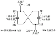
如图6的(a)所示,N+累积型MOS电容元件310布置在下部半导体基板220上。如图7所示,当假设MOS电容元件310的靠近下部半导体基板220的安装MOS电容元件310一侧的电极为下部电极312时,例如,安装在元件分隔部311上的下部电极312是形成在p型阱228中的n型扩散层,在下部电极312上存在由氧化硅(SiO2)制成的栅极绝缘膜316,并且在栅极绝缘膜316上形成由n型多晶硅制成的上部电极313。在MOS电容元件310的动作中,在下部电极312的表面累积电子,因此将MOS电容元件310称为N+累积型MOS电容。As shown in (a) of FIG. 6 , the N+ accumulation type
在配置有MOS电容元件310的相同区域中,在形成作为上层的布线(M1至M6)224的区域中,安装有MIM(金属绝缘金属)电容元件320,该MIM电容元件320通过堆叠位于更靠近下部半导体基板220一侧的下部电极322、绝缘膜(包括高K材料)、以及上部电极321而形成。所述绝缘膜为Ta2O2、Nb2O3、ZrO2、HfO2、La2O3、Pr2O3、Al2O3、SiO2、SiN中的任意一种的单层膜或多个堆叠膜。如图9中所示,下部电极322和上部电极321是Cu、Al、Ti、TiN、Ta和TaN中的任一种的单层膜或多个堆叠膜。In the same area where the
布线(M5)224设置有负(Minus)端子225和正(Plus)端子226。The wiring ( M5 ) 224 is provided with a negative (Minus) terminal 225 and a positive (Plus)
要注意的是,除了MIM电容元件320之外,还可使用图8中所示的梳状布线(MOM)电容元件330或图10中所示的PIP(多绝缘体多)电容元件340。It is to be noted that, instead of the
如图11所示,通过将N+累积型MOS电容元件310的下部电极312和MIM电容元件320的上部电极321通过过孔315和布线(M6)224连接,并且将MOS电容元件310的上部电极313和MIM电容元件320的下部电极322利用过孔314和布线(M5)224连接,从而将两个电容元件并联连接。采用以这种方式构造的电容元件具有以下优点。As shown in Figure 11, by connecting the
第一个优点是增加电容元件的每单位面积的电容密度。例如,如果MOS电容元件310的电极之间的电位差为3V时的电容值为100fF,MIM电容元件320的电极之间的电位差为3V时的电容值为100fF,则两个电容元件(MOS电容元件310和MIM电容元件320)并联连接并以3V操作时的电容值为200fF,这表示电容密度的两倍增加。因而,与通过减小MOS电容元件310和MIM电容元件320的电极之间的绝缘膜的膜厚度来增加电容密度的情况相比,可在不缩短TDDB的寿命的情况下增加电容密度。The first advantage is to increase the capacitance density per unit area of the capacitive element. For example, if the potential difference between the electrodes of the
第二个优点是可以减小电容值的偏置依赖性。这是由于以下机制。图12的(a)表示N+累积型MOS电容元件310的C-V特性。横轴表示电极之间的电位差,并且纵轴表示当电位差为-3V时通过电容值标准化的数值。当下部电极312固定在0V并且上部电极313的电位在-3V与3V之间变化时,电容值的偏置依赖性具有正斜率,如由实线A所描绘的。另一方面,关于MIM电容元件320的C-V特性,当如图12的(b)所示下部电极322固定在0V且上部电极321的电位在-3V与3V之间变化时斜率为正,而当上部电极321固定在0V且下部电极的电位在-3V与3V之间变化时斜率变为负,如虚线C所示。A second advantage is that the bias dependence of the capacitance value can be reduced. This is due to the following mechanism. (a) of FIG. 12 shows the C-V characteristic of the N+ accumulation type
换言之,在图11所示的并联连接状态下,当负端子225设置为0V且正端子226在-3V和3V之间变化时,由于N+累积型MOS电容元件310的电容值的偏置依赖性和MIM电容元件320的电容值的偏置依赖性彼此抵消,其C-V特性表现出图13所示的A//C,并且可以形成电容值具有低电压依赖性的电容元件。In other words, in the parallel connection state shown in FIG. 11 , when the
如上所述,能够改变并联连接的各个MOS电容元件310和各个MIM电容元件320的连接,并且能够改变其电容值的偏置依赖性的斜率的符号,并且通过并联连接具有不同的斜率MOS电容元件310和MIM电容元件320,能够降低的电容值作为整体的偏置依赖性。As described above, the connection of each
可以降低作为整体的元件的电容值的Ctotal(V)/Ctotal(0)的偏置依赖性的多少这取决于并联连接的各电容元件的电容密度、元件大小、偏置依赖性系数,其期望遵循以下给出的等式。因此,设计者可以通过优化每个电容元件的元件尺寸来获得期望的特性。How much the bias dependence of Ctotal(V)/Ctotal(0) of the capacitance value of the element as a whole can be reduced depends on the capacitance density, element size, and bias dependence coefficient of each capacitance element connected in parallel, and its desired Follow the equation given below. Therefore, a designer can obtain desired characteristics by optimizing the element size of each capacitive element.
Ctotal(V)/Ctotal(0)=ΣAn×Cn(V)×Sn/Cn(0)×SnCtotal(V)/Ctotal(0)=ΣAn×Cn(V)×Sn/Cn(0)×Sn
Ctotal(V)/Ctotal(0)元件整体的电容值的偏置依赖性(基于电位差的标准值=0V)Ctotal(V)/Ctotal(0) The bias dependence of the capacitance value of the entire element (standard value based on potential difference = 0V)
Ctotal(V)在电极之间的电位差是工作电压V时元件整体的电容值Ctotal (V) The potential difference between the electrodes is the overall capacitance value of the element at the working voltage V
Ctotal(0)当电极之间的电位差是0V时元件整体的电容值Ctotal(0) When the potential difference between the electrodes is 0V, the overall capacitance value of the element
Cn(V)在电极之间的电位差是工作电压V时每个电容元件的电容密度The potential difference of Cn(V) between the electrodes is the capacitance density of each capacitive element at the working voltage V
Sn每个电容元件的元件尺寸Sn element size of each capacitive element
An每个电容元件的电容值的偏置依赖性系数(包括正或负)An bias dependence coefficient (both positive and negative) of the capacitance value of each capacitive element
此外,尽管图6示出了其中两个不同的电容元件(MOS电容元件310和MIM电容元件320)被安排在同一区域中的实例,但电容元件不必被安排在同一区域中。Furthermore, although FIG. 6 shows an example in which two different capacitive elements (
<第一实施方式引起的操作优点><Operational advantages due to the first embodiment>
如上所述,根据第一实施例,通过与N+累积型MOS电容元件310并联连接,具有与MOS电容元件310的C-V特性相反的特性的MIM电容元件320抵消偏置特性,并且实现具有平坦偏置特性的电容元件。此外,与通过减小电容元件的电极之间的绝缘膜的膜厚度而增加电容密度的情况相比,可在不缩短TDDB的寿命的情况下增加电容密度。因此,可以实现电容值具有低偏置依赖性并具有高电容密度而不降低工作电压的电容元件。As described above, according to the first embodiment, by connecting in parallel with the N+ accumulation type
此外,根据第一实施例,可以优化每个电容元件的装置结构和尺寸以及各个电容元件之间的连接方法,使得电容元件整体的C-V特性最接近1。Furthermore, according to the first embodiment, the device structure and size of each capacitive element and the connection method between the respective capacitive elements can be optimized so that the overall C-V characteristic of the capacitive element is closest to 1.
<第一变形例><First modified example>
图14是根据第一实施方式的第一变形例的固态成像装置100的截面图。在图14中,与图6的(a)中的上述那些相同的部分用相同的附图标记表示,并且将省略其详细描述。FIG. 14 is a cross-sectional view of a solid-
在图14中,固态成像装置100具有其中使用下部半导体基板220上的布线(M1至M4)224形成图8中所示的MOM电容元件330并且MOM电容元件330并联连接至N+累积型MOS电容元件310和MIM电容元件320的结构。在这种情况下,如图15所示,MOM电容元件330的上部电极331通过过孔315和布线(M6)224连接到MOS电容元件310的下部电极312和MIM电容元件320的上部电极321。此外,MOM电容元件330的下部电极332通过过孔314和布线(M6)224连接到MOS电容元件310的上部电极313和MIM电容元件320的下部电极322。通过采用这种结构,能够进一步提高电容密度。In FIG. 14 , the solid-
如图16的(b)所示,在普通MOM电容元件330的C-V特性中,电容值的偏置依赖性极低,而不管施加在电极之间的偏置是正还是负。在这种状态下,C-V特性类似于在上述图16的(a)中示出的当并联连接N+累积型MOS电容元件310和MIM电容元件320时的特性。因此,即使将MOM电容元件330加到要并联连接的电容元件,电容元件的电容值的偏置依赖性总体上也不会显著增加。此外,因为在电极之间施加正偏置与施加负偏置之间,上述电容值的偏置依赖性没有显著不同,所以不需要意识到电极的连接方法,并且任何电极可以连接至正(Plus)端子226。As shown in (b) of FIG. 16 , in the C-V characteristic of the general
<第二变形例><Second modification>
图17是根据第一实施例的第二变形例的固态成像装置100的截面图。在图17中,与上述图6的(a)中的那些相同的部分由相同的参考符号表示并且将省略其详细描述。FIG. 17 is a cross-sectional view of a solid-
在图17中,固态成像装置100采用空穴累积型MOS电容元件360(称为P+累积型MOS电容)。在MOS电容元件360中,靠近下部半导体基板220的一侧的下部电极362是在n型阱229中形成的p型扩散层,由氧化硅(SiO2)制成的栅极绝缘膜366存在于下部电极362上,并且由p型多晶硅制成的上部电极363形成在栅极绝缘膜366上。In FIG. 17, the solid-
如图18所示,MOS电容元件360的上部电极363通过过孔364和布线(M6)224连接到MIM电容元件320的上部电极321。此外,MOS电容元件360的下部电极362通过过孔365和布线(M6)224连接到MIM电容元件320的下部电极322。As shown in FIG. 18 , the
在MOS电容元件360中,在工作期间在下部电极362的表面上积累空穴。关于其C-V特性,如图19所示,当下部电极362固定在0V并且上部电极363的电位在-3V和3V之间变化时,电容值的偏置依赖性的符号为负(虚线D)。另一方面,当MIM电容元件320的下部电极322固定在0V且上部电极321的电位在-3V和3V之间变化时,电容值的偏置依赖性的符号为正(实线B)。因此,通过将两个电容元件320和360的上部电极和下部电极相互并联连接,可以减小电容值的偏置依赖性。In the
<第三变形例><Third modification>
图20是根据第一实施例的第三变形例的固态成像装置100的截面图。在图20中,与上述图6的(a)中的那些相同的部分由相同的参考符号表示并且将省略其详细描述。FIG. 20 is a cross-sectional view of a solid-
在图20中,在固态成像装置100中,形成在不同层上的两个MIM电容元件320和350的电极反向连接。如图21所示,MIM电容元件320的下部电极322通过布线(M4)224和布线(M6)224连接到MIM电容元件350的上部电极351。另外,MIM电容元件320的上部电极321经由布线(M3)224和布线(M6)224连接到MIM电容元件350的下部电极352。In FIG. 20 , in the solid-
当MIM电容元件320的下部电极322固定在0V且上部电极321的电位在-3V和3V之间变化时,电容值的偏置依赖性的符号为正(实线B),如图22所示。另一方面,当MIM电容元件350的上部电极351固定在0V且下部电极352的电位在-3V和3V之间变化时,电容值的偏置依赖性的符号为负(虚线C)。When the
因此,当MIM电容元件320的上部电极321和MIM电容元件350的下部电极352彼此连接时,由于电容值的偏置依赖性的符号在并联连接的电容元件的电容值的偏置依赖性方面在元件之间不同,所以可减小电容值的偏置依赖性。Therefore, when the
<第四变形例><Fourth modification>
图23是根据第一实施方式的第四变形例的固态成像装置100的截面图。在图23中,与上述图6的(a)中的那些相同的部分由相同的参考符号表示并且将省略其详细描述。FIG. 23 is a cross-sectional view of a solid-
在图23中,固态成像装置100表示利用PIP(多绝缘体多)电容元件340的实例。如图10所示,PIP电容元件340是以多晶硅作为电极的电容元件,例如,通过顺序堆叠作为下部电极342的N型多晶Si、作为绝缘膜的SiO2和作为上部电极的N型多晶Si而形成。PIP电容元件340的特征是电容值的偏置依赖性低。In FIG. 23 , the solid-
如图24所示,PIP电容元件340的上部电极343通过布线(M3)224与MIM电容元件350的下部电极352连接。另外,PIP电容元件340的下部电极342经由布线(M4)224连接到MIM电容元件350的上部电极351。As shown in FIG. 24 , the
因此,当应用于本公开的第一实施例时,PIP电容元件340执行与MOM电容元件330相同的作用。换句话说,如图25所示,通过添加PIP电容元件340作为并联连接的一个电容元件,可增加电容元件整体的电容值,而不显著增加电容元件整体的电容值的偏置依赖性。在并联连接PIP电容元件340时的连接方法中,可以与MOM电容元件330类似的方式将下部电极342和上部电极343中的任一者连接到正(Plus)侧。Therefore, the
此外,当并联连接N+累积型MOS电容元件310和P+累积型MOS电容元件360时,仅并联连接MOS电容元件310的上部电极313和MOS电容元件360的上部电极363,并联连接MOS电容元件310的下部电极312和MOS电容元件360的下部电极362可能就足够了。In addition, when the N+ accumulation type
<第二实施方式><Second Embodiment>
图26是根据第二实施方式的固态成像装置100的截面图。在图26中,与上述图14中的那些相同的部分由相同的参考符号表示,并且将省略其详细描述。FIG. 26 is a cross-sectional view of the solid-
作为第二实施例,将描述利用WoW技术将布置在两个不同芯片上的多个电容元件全部并联连接的实例。As a second embodiment, an example in which a plurality of capacitive elements arranged on two different chips are all connected in parallel using WoW technology will be described.
图26表示,在堆叠型图像传感器中,电容元件安装在上部半导体基板210和下部半导体基板220的芯片上的实例以及安装在上部半导体基板210和下部半导体基板220上的电容元件使用布置在接合表面上的金属接合部230并联连接。26 shows an example in which capacitive elements are mounted on chips of an
在图26中,上部半导体基板210由上至下由p型阱32、眉间绝缘膜213、以及布线层214构成。在上部半导体基板210的下侧设置有N+累积型MOS电容元件410。假设MOS电容元件410的靠近下部半导体基板220的安装MOS电容元件410的一侧的电极为下部电极412时,下部电极412为形成在p型阱32中的n型扩散层,在下部电极412上存在由氧化硅(SiO2)制成的栅极绝缘膜416,在栅极绝缘膜416上形成由n型多晶硅制成的上部电极413。In FIG. 26 , an
在形成布线(M1至M4)215的区域中,使用布线(M1至M4)215形成MOM电容器元件420,布线(M1至M4)215是在与形成MOS电容器元件410的相同区域中的上部半导体基板210的一侧相反的一侧的层。在这种情况下,如图27所示,MOM电容元件420的上部电极421通过过孔414与MOS电容元件410的上部电极413连接。此外,MOM电容元件420的下部电极422经由过孔415连接到MOS电容元件410的下部电极412。In the region where the wiring (M1 to M4) 215 is formed, the
此外,MOS电容元件410的上部电极413和MOM电容元件420的上部电极421通过由铜(Cu)制成的金属接合部231和232连接至下部半导体基板220侧的MIM电容元件320的下部电极322和MOS电容元件310的上部电极313、MOM电容元件330的上部电极331。此外,MOS电容元件410的下部电极412和MOM电容元件420的下部电极422通过由铜(Cu)制成的金属接合部231和232连接至下部半导体基板220侧的MOM电容元件330的下部电极332和MOS电容元件310的下部电极312、MIM电容元件320的上部电极321。In addition, the
由于这样的连接,例如,当负(Minus)端子225固定在0V且正(Plus)端子226从-3V变化到3V时,每个电容元件的电容值的偏置依赖性的符号,N+累积型MOS电容元件310和410是正的,但MIM电容元件320是负的。假设MOM电容元件330和420的偏置依赖性低且可忽略,由于N+累积型MOS电容元件310和410的偏置依赖性斜率的符号与MIM电容元件320的偏置依赖性斜率的符号相反,所以优化这些元件的元件大小使得由并联连接这些元件形成的电容元件的作为整体的电容值的偏置依赖性变得非常低。Due to such connection, for example, when the negative (Minus) terminal 225 is fixed at 0V and the positive (Plus)
此外,通过将这些电容元件布置在相同区域中,因为与第一实施例相比,上部半导体基板210(传感器部)的MOS电容元件410和MOM电容元件420的电容值也可以被相加,所以可以形成具有甚至更高电容密度的电容值。例如,在图26的情况下,若N+累积型MOS电容元件310和N+累积型MOS电容元件410的电容值为100fF,MOM电容元件330和MOM电容元件420的电容值为30fF,MIM电容元件320的电容值为100fF,则并联电容元件的总电容值为独立使用N+累积型MOS电容元件310时电容值的3.6倍。Furthermore, by arranging these capacitive elements in the same area, since the capacitance values of the
<根据第二实施方式的操作优点><Operational Advantages According to Second Embodiment>
如上所述,根据第二实施例,通过不仅并联连接安装在下部半导体基板220上的N+累积型MOS电容元件310、MIM电容元件320和MOM电容元件330,而且并联连接安装在上部半导体基板210上的MOS电容元件410和MOM电容元件420,与第一实施例相比,可形成具有更高电容密度的电容值。As described above, according to the second embodiment, by connecting not only the N+ accumulation type
<第二实施方式的第一变形例><First Modification of Second Embodiment>
图28是根据第二实施方式的第一变形例的固态成像装置100中的截面图。在图28中,与上述图26中的那些相同的部分用相同的参考符号表示,并且将省略其详细描述。FIG. 28 is a sectional view in a solid-
在图28中,在固态成像装置100中,与第一实施例中相同的N+累积型MOS电容元件310和MOM电容元件330安装到下部半导体基板220(外围电路部),并且P+累积型MOS电容元件430和MOM电容元件420安装到上部半导体基板210(传感器部)。在MOS电容元件430中,接近上部半导体基板210一侧的下部电极431是P型扩散层,在下部电极431上存在由氧化硅(SiO2)构成的栅极绝缘膜436,在栅极绝缘膜436上形成由P型多晶硅构成的上部电极432。In FIG. 28, in the solid-
如图29所示,MOM电容元件420的上部电极421通过过孔414与MOS电容元件430的上部电极432连接。此外,MOM电容元件420的下部电极422通过过孔415连接到MOS电容元件430的下部电极431。As shown in FIG. 29 , the
此外,MOS电容元件430的上部电极432和MOM电容元件420的上部电极421通过由铜(Cu)制成的金属接合部231和232连接至下部半导体基板220侧的MOS电容元件310的上部电极313和MOM电容元件330的上部电极331。此外,MOS电容元件430的下部电极431和MOM电容元件420的下部电极422通过由铜(Cu)制成的金属接合部231和232连接至下部半导体基板220侧的MOS电容元件310的下部电极312和MOM电容元件330的下部电极332。Further, the
<第二实施方式的第一变形例导致的操作优点><Operational advantages resulting from the first modified example of the second embodiment>
归因于这种连接,当负(Minus)端子225固定在0V且正(Plus)端子226从-3V改变为3V时,作为每一电容元件的电容值的偏置依赖性的符号,N+累积型MOS电容元件310为正,P+累积型MOS电容元件430为负。假设MOM电容元件330和420的偏置依赖性低且可忽略不计,由于N+累积型MOS电容元件310和P+累积型MOS电容元件430的偏置依赖性的斜率的符号相反,所以优化这些元件的元件尺寸使得能够使通过并联连接这些元件形成的电容元件作为整体的电容值的偏置依赖性显著地低。Due to this connection, when the negative (Minus) terminal 225 is fixed at 0V and the positive (Plus)
<第二实施方式的第二变形例><Second Modification of Second Embodiment>
图30是根据第二实施方式的第二变形例的固态成像装置100中的截面图。在图30中,与上述图30中的那些相同的部分由相同的参考符号表示,并且将省略其详细描述。FIG. 30 is a cross-sectional view in a solid-
在图30中,固态成像装置100使设置在接合表面上的下部半导体基板220一侧上的金属接合部512和上部半导体基板210一侧的金属接合部511彼此相对,从而使金属接合部511和512用作电容元件,并且将电容元件与其他电容元件并联连接以进一步增加电容密度。该电容元件将被称为接合部电容元件510。在这种情况下,假定上部半导体基板210侧的金属接合部511是上部电极,并且假定下部半导体基板220侧的金属接合部512是下部电极。In FIG. 30 , the solid-
如图31所示,接合部电容元件510的上部电极(金属接合部511)通过过孔414与MOS电容元件410的上部电极413和MOM电容元件420的上部电极421连接。另外,接合部电容元件510的下部电极(金属接合部512)通过过孔415连接到MOS电容元件410的下部电极412和MOM电容元件420的下部电极422。As shown in FIG. 31 , the upper electrode (metal junction 511 ) of junction capacitance element 510 is connected to
并且,接合部电容元件510的上部电极(金属接合部511)与在下部半导体基板220侧的MOM电容元件330的上部电极331、MOS电容元件310的上部电极313、MIM电容元件320的下部电极322连接。另外,接合部电容元件510的下部电极(金属接合部512)连接到在下部半导体基板220侧的MOM电容元件330的下部电极332,MOS电容元件310的下部电极312、MIM电容元件320的上部电极321。In addition, the upper electrode (metal junction 511) of the junction capacitive element 510 is connected to the
接合部电容元件510通过简单地使金属材料彼此相对而被赋予电容元件的功能,并且电容值的偏置依赖性以类似于MOM电容元件330和420的方式极低。因此,通过并联连接接合部电容元件510,电容密度增加,而不显著改变作为连接源的电容元件的电容值的偏置依赖性。The junction capacitive element 510 is given the function of a capacitive element by simply making metal materials face each other, and the bias dependence of the capacitance value is extremely low in a manner similar to the MOM capacitive
<第二实施方式的第二变形例的操作优点><Operational Advantages of Second Modification of Second Embodiment>
如上所述,根据第二实施例的第二变形例,通过用接合部电容元件510代替上部半导体基板210和下部半导体基板220的金属接合部511和512,能够增加电容元件整体的电容值。As described above, according to the second modification of the second embodiment, by replacing the
<第二实施方式的另一应用实例><Another application example of the second embodiment>
本公开的第二实施方式不限于在本文中所描述的内容。例如,图32是描述使用通常的CMOS工艺分别可安装到上部半导体基板210(芯片1)和下部半导体基板220(芯片2)的电容元件的表格。The second embodiment of the present disclosure is not limited to what is described herein. For example, FIG. 32 is a table describing capacitive elements respectively mountable to the upper semiconductor substrate 210 (chip 1 ) and the lower semiconductor substrate 220 (chip 2 ) using a general CMOS process.
当各个电容元件的上部电极连接至Plus端子并且各个电容元件的下部电极连接至负(Minus)端子225时,图32所示的表格中的电极连接方向是“正向”。相反,当各个电容元件的上部电极连接至负(Minus)端子225并且各个电容元件的下部电极连接至正(Plus)端子226时,电极连接方向是“反向”。电容值具有极低偏置依赖性并且可连接至任一端子而不发生事件的元件被描述为“忽略”。When the upper electrode of each capacitive element is connected to the Plus terminal and the lower electrode of each capacitive element is connected to the negative (Minus) terminal 225, the electrode connection direction in the table shown in FIG. 32 is "positive". On the contrary, when the upper electrode of each capacitive element is connected to the negative (Minus) terminal 225 and the lower electrode of each capacitive element is connected to the positive (Plus)
此外,电容值的偏置依赖性的斜率的符号表示当根据由电极连接方向描述的连接将负(Minus)端子225描述为0V并且将正(Plus)端子226从-3V改变为3V时的电容值的偏置依赖性的符号。Also, the sign of the slope of the bias dependence of the capacitance value represents the capacitance when the negative (Minus) terminal 225 is described as 0V and the positive (Plus)
从图32中所示的表格中,显而易见的是,在堆叠两个芯片的堆叠结构中,存在根据期望的连接方法并联连接并且满足设定为目标的电容密度和电容值的偏置相关性两者的多个电容元件的极大数量的组合。虽然在实施例中不能描述所有这样的组合,但是设计者可以考虑到要设计的电路所要求的特性、可用的芯片面积和安装每个元件的制造成本,做出最好的可能选择。From the table shown in FIG. 32, it is apparent that in a stacked structure in which two chips are stacked, there are two bias dependencies that are connected in parallel according to a desired connection method and satisfy the capacitance density and capacitance value set as targets. or a very large number of combinations of multiple capacitive elements. Although not all such combinations can be described in the embodiments, the designer can make the best possible choice in consideration of the required characteristics of the circuit to be designed, the available chip area, and the manufacturing cost of mounting each component.
<第三实施方式><Third Embodiment>
在本公开的第三实施方式中,将描述固态成像装置,其中,光电转换元件和放大来自光电转换元件的信号的放大晶体管设置在不同的基板上,并且使用WoW技术堆叠安装有传感器部(其中设置光电转换元件和传输门(TRG))、像素晶体管部(其中设置诸如放大晶体管的像素晶体管)、以及外围电路部(其中设置处理来自放大晶体管的信号的信号处理电路)的三个基板。In a third embodiment of the present disclosure, a solid-state imaging device will be described in which a photoelectric conversion element and an amplification transistor that amplifies a signal from the photoelectric conversion element are provided on different substrates, and a sensor section (wherein Three substrates are provided, a photoelectric conversion element and a transmission gate (TRG), a pixel transistor section in which a pixel transistor such as an amplification transistor is provided, and a peripheral circuit section in which a signal processing circuit processing a signal from the amplification transistor is provided.
图33是根据第三实施方式的固态成像装置100A中的截面图。图33的(a)示出了像素的外部并且图33的(b)示出了像素的内部。在图33中,与上述图26中的那些相同的部分由相同的参考符号表示,并且将省略其详细描述。FIG. 33 is a sectional view in a solid-
固态成像装置100A从上到下由传感器部610、像素晶体管部620和外围电路部630组成。如图34所示,固态成像装置100A由堆叠型图像传感器构成,其中,堆叠作为传感器部610、像素晶体管部620和外围电路部630的三个半导体芯片,并且布线的一部分通过金属接合部640电连接。如图35所示,传输晶体管T1、光电转换元件D1和浮动扩散FD 34被布置在传感器部610中。复位晶体管T2、放大晶体管T3和选择晶体管T4布置在像素晶体管部620中。The solid-
返回至图33,传感器部610从上到下由光电转换层611和眉间绝缘膜612组成。光电转换层211是其上形成光电二极管(PD)31并且由于光电转换根据入射光的光强度产生电荷的层。对于每个像素30,PD 31由形成在的光电转换层611内部的元件分离部33a和33b电分离。此外,传输晶体管T1的栅极电极36和FD 34形成在光电转换层611上。应注意,如图33的(a)所示,在像素30的外部仅存在P型阱32。传输晶体管T1形成在眉间绝缘膜612上。Returning to FIG. 33 , the
像素晶体管部620由上至下由p型阱621和布线层622构成。在p型阱621中形成n型扩散层。布线层622被配置为包括多层堆叠的布线(M1至M4)623。构成每个像素30的传输晶体管T1、复位晶体管T2、放大晶体管T3、以及选择晶体管T4经由形成在布线层622中的多层布线(M1至M4)623驱动。另外,在接合到外围电路部630的布线层622的内部提供由铜(Cu)制成的金属接合部641。The
另一方面,外围电路部630从上到下由眉间绝缘膜和布线层构成。布线层被配置为包括多层堆叠的所有布线631和布线(M1至M6)632。此外,眉间绝缘膜设置有待接合至像素晶体管部620的金属接合部641的由铜(Cu)制成的金属接合部642。On the other hand, the
在如上所述配置的固态成像装置100A中,当入射至传感器部610的光被PD 31光电转换时,产生电荷。此外,所生成的电荷由图1中所示的信号线LSGN作为像素信号经由放大晶体管T3输出至形成在外围电路部630中的ADC群150,由外围电路部630的布线(M1至M4)623和布线(M1至M6)632形成信号线LSGN。In the solid-
如图33的(a)所示,在外围电路部630上配置N+累积型MOS电容元件310。MOM电容元件330和MIM电容元件320布置在MOS电容元件310上方的层中。As shown in (a) of FIG. 33 , the N+ accumulation type
N+累积型MOS电容元件410布置在像素晶体管部620的下侧。在形成布线(M1至M4)623的区域中,使用布线(M1至M4)623形成MOM电容器元件420,布线(M1至M4)623是在与形成MOS电容器元件410的相同区域中的像素晶体管部620的一侧相反的一侧的层。在这种情况下,如图36所示,MOM电容元件420的上部电极421通过过孔414与MOS电容元件410的上部电极413连接。此外,MOM电容元件420的下部电极422通过过孔415连接到MOS电容元件410的下部电极412。The N+ accumulation type
此外,MOS电容元件410的上部电极413和MOM电容元件420的上部电极421经由由铜(Cu)制成的金属接合部641和642连接到外围电路部630侧的MOS电容元件310的上部电极313、MIM电容元件320的下部电极322和MOM电容元件330的上部电极331。此外,MOS电容元件410的下部电极412和MOM电容元件420的下部电极422经由由铜(Cu)制成的金属接合部641和642连接到外围电路部630侧的MOS电容元件310的下部电极312、MIM电容元件320的上部电极321和MOM电容元件330的下部电极332。Further, the
<根据第三实施方式的操作优点><Operational Advantages According to Third Embodiment>
如上所述,根据第三实施例,获得与上述第二实施例类似的操作优点,并且作为当负(Minus)端子225固定在0V且正(Plus)端子226从-3V变化到3V时,作为每个电容元件的电容值的偏置依赖性的符号,N+累积型MOS电容元件310和N+累积型MOS电容元件410是正的,但是MIM电容元件320是负的,如第一实施例中所述。假设MOM电容元件330和420的偏置依赖性低且可忽略,由于N+累积型MOS电容元件310和N+累积型MOS电容元件410的偏置依赖性斜率的符号与MIM电容元件320的偏置依赖性斜率的符号相反,所以优化这些元件的元件尺寸使得能够使通过并联连接这些元件形成的电容元件作为整体的电容值的偏置依赖性显著地低。As described above, according to the third embodiment, similar operational advantages to those of the above-described second embodiment are obtained, and as The sign of the bias dependence of the capacitance value of each capacitive element, the N+ accumulation type
如上所述,甚至三层堆叠型图像传感器也可安装有电容值大且电容值的偏置依赖性低的电容元件。As described above, even a three-layer stack type image sensor can be mounted with a capacitive element having a large capacitance value and low bias dependence of the capacitance value.
<第四实施例><Fourth Embodiment>
在本公开的第四实施方式中,将描述应用于使用SPAD(单光子雪崩二极管)的光检测设备的固态成像设备。In a fourth embodiment of the present disclosure, a solid-state imaging device applied to a photodetection device using a SPAD (Single Photon Avalanche Diode) will be described.
图37示出了构成根据第四实施方式的固态成像装置100B的每个电路的半导体芯片上的布置图。根据第四实施方式的固态成像装置100B由堆叠型图像传感器构成,其中,堆叠作为上部半导体基板710和下部半导体基板720的两个半导体芯片,并且通过作为TSV(硅过孔)等的金属接合部730电连接上部和下部芯片的布线的一部分。在这种情况下,SPAD光电二极管41以矩阵图案布置在上部半导体基板710上,并且除了SPAD光电二极管41之外的外围电路51(诸如ADC群150和信号处理电路180)安装至下部半导体基板720。FIG. 37 shows a layout diagram on a semiconductor chip constituting each circuit of the solid-
图38是根据第四实施方式的固态成像装置100B中的截面图。图38的(a)示出了像素的外部并且图38的(b)示出像素的内部。FIG. 38 is a cross-sectional view in a solid-
在图38中,上部半导体基板710从上至下由光电转换层711、眉间绝缘膜713和布线层714构成。光电转换层711是在其上形成SPAD光电二极管41并且检测入射光(光子)并且使用雪崩倍增将从入射光生成的载流子转换成电信号脉冲的层。对于每个像素30,SPAD光电二极管41由形成在光电转换层711内部的p型扩散层42a和n型扩散层42b电分离。应注意,如图38的(a)所示,在像素30的外部仅存在P型阱43。In FIG. 38 , an
由SPAD光电二极管41生成的电信号脉冲经由形成在眉间绝缘膜713中的过孔716被输出至形成在布线层714中的布线(M1至M4)715。由铜(Cu)制成的金属接合部731设置在布线层714的内部,以执行与下部半导体基板720的接合。The electric signal pulse generated by the
另一方面,下部半导体基板720由上至下由眉间绝缘膜721和布线层722构成。布线层722被配置为包括堆叠成多层的所有布线723和布线(M1至M6)724。此外,眉间绝缘膜721设置有待接合至上部半导体基板710的金属接合部731的由铜(Cu)制成的金属接合部732。On the other hand, the
在如上所述配置的固态成像装置100B中,由于SPAD光电二极管41光电转换由上部半导体基板210检测的光,所以生成电信号脉冲。此外,电信号脉冲经由图1所示的由下部半导体基板720的布线(M1至M4)715和布线(M1至M6)724形成的信号线LSGN输出至外围电路51。In the solid-
如图38的(a)所示,在下部半导体基板720上设置N+累积型MOS电容元件310。MIM(Metal Insulator Metal,金属绝缘体金属)电容元件320安装在形成布线(M1至M6)724的区域中,布线724是在布置MOS电容元件310的相同区域中的上层,通过堆叠位于更靠近下部半导体基板220的一侧附近的下部电极322、绝缘膜(包括高K材料)和上部电极321形成MIM电容元件320。As shown in (a) of FIG. 38 , an N+ accumulation type
如图39所示,利用过孔315和布线(M6)724将N+累积型MOS电容元件310的下部电极312和MIM电容元件320的上部电极321连接,利用过孔314和布线(M5)724将MOS电容元件310的上部电极313和MIM电容元件320的下部电极322连接,从而将两个电容元件并联连接。As shown in FIG. 39 , the
<根据第四实施例的操作优点><Operational Advantages According to Fourth Embodiment>
如上所述,根据第四实施例,可以获得与先前所述的第一实施例类似的操作优点,并且可以实现具有高电容密度和极低偏置依赖性的电容元件。As described above, according to the fourth embodiment, similar operational advantages to those of the previously described first embodiment can be obtained, and a capacitive element having a high capacitance density and extremely low bias dependence can be realized.
<第五实施方式><Fifth Embodiment>
第一至第四实施方式举例说明根据本技术的半导体装置应用于作为电子设备的实例的固态成像装置的情况。在第五实施方式中,将举例说明根据本技术的半导体装置应用于其他电子设备的情况。The first to fourth embodiments exemplify cases where the semiconductor device according to the present technology is applied to a solid-state imaging device as an example of electronic equipment. In the fifth embodiment, a case where the semiconductor device according to the present technology is applied to other electronic equipment will be exemplified.
例如,根据本技术的半导体装置可以应用于构成通用滤波器电路的电容器。如图40所示,通用滤波电路包括电阻器R11和电容器C11,并且根据本技术的半导体装置可以用作电容器C11的部件。将根据本技术的半导体装置应用于构成滤波器电路的电容器C11使得能够实现大电容并且进一步加宽通带。For example, a semiconductor device according to the present technology can be applied to a capacitor constituting a general-purpose filter circuit. As shown in FIG. 40 , a general-purpose filter circuit includes a resistor R11 and a capacitor C11 , and the semiconductor device according to the present technology can be used as a component of the capacitor C11 . Applying the semiconductor device according to the present technology to the capacitor C11 constituting the filter circuit enables realization of large capacitance and further widening of the passband.
此外,根据本技术的半导体装置可以应用于构成普通平滑电路的电容器。如图41所示,一般的滤波电路包括二极管D21和电容器C21,并且根据本技术的半导体装置可以用作电容器C21的部件。将根据本技术的半导体装置应用于构成滤波电路的电容器C21使得能够实现大电容并且将交流电准确地转换成直流电。Furthermore, the semiconductor device according to the present technology can be applied to capacitors constituting general smoothing circuits. As shown in FIG. 41, a general filter circuit includes a diode D21 and a capacitor C21, and the semiconductor device according to the present technology can be used as a component of the capacitor C21. Applying the semiconductor device according to the present technology to the capacitor C21 constituting the filter circuit makes it possible to realize a large capacitance and accurately convert alternating current into direct current.
此外,根据本技术的半导体装置可以应用于构成一般积分电路的电容器。如图42所示,通用积分电路包括电阻器R32、电容器C31、以及运算放大器800,并且根据本技术的半导体装置可以用作电容器C31的部件。Furthermore, the semiconductor device according to the present technology can be applied to a capacitor constituting a general integrating circuit. As shown in FIG. 42 , a general integrating circuit includes a resistor R32, a capacitor C31, and an
<其他实施方式><Other Embodiments>
尽管上面以第一实施方式至第四实施方式、第一实施方式的变形、以及第二实施方式的变形的形式描述了本技术,然而,应当理解的是,构成本公开的一部分的描述和附图限制了本技术。当理解上述第一实施方式至第四实施方式公开的技术内容的目的时,对本领域技术人员显而易见的是,各种替代实施方式、实施例和可操作技术包括在本技术中。此外,在不矛盾的范围内,可以适当地组合在第一至第四实施方式、第一实施方式的变形例以及第二实施方式的变形例中分别公开的配置。例如,可以组合在多个不同实施方式中公开的配置,或者可以组合在相同实施方式的多个不同变形中公开的配置。Although the present technology has been described above in the form of the first embodiment to the fourth embodiment, the modification of the first embodiment, and the modification of the second embodiment, it should be understood that the description and accompanying drawings constitute a part of the present disclosure. Figures limit the present technique. When understanding the purpose of the technical contents disclosed in the first to fourth embodiments described above, it will be apparent to those skilled in the art that various alternative embodiments, examples, and operational techniques are included in the present technology. Furthermore, the configurations respectively disclosed in the first to fourth embodiments, the modification of the first embodiment, and the modification of the second embodiment may be appropriately combined within a range that does not contradict. For example, configurations disclosed in multiple different embodiments may be combined, or configurations disclosed in multiple different variations of the same embodiment may be combined.
<电子设备的应用实例><Application examples of electronic equipment>
接下来,将描述根据本公开的第六实施方式的电子设备。图43是根据本公开的第六实施方式的电子设备1000的示意性配置图。Next, an electronic device according to a sixth embodiment of the present disclosure will be described. FIG. 43 is a schematic configuration diagram of an
根据第六实施方式的电子设备1000包括固态成像装置1010、光学透镜1020、快门装置1030、驱动电路1040以及信号处理电路1050。根据第六实施方式的电子设备1000表示在其中根据本公开的第一实施方式的固态成像装置100被用在电子设备(例如,照相机)中作为固态成像装置1010的情况下的实施方式。An
光学透镜1020在固态成像装置1010的成像表面上形成来自对象的图像光(入射光1060)的图像。因此,信号电荷在设定时间段内积聚在固态成像装置1010中。快门装置1030控制对固态成像装置1010的光照射时段和光阻挡时段。驱动电路1040提供用于控制固态成像装置1010的传输操作和快门装置1030的快门操作的驱动信号。通过从驱动电路1040供应的驱动信号(定时信号)执行固态成像装置1010的信号传输。信号处理电路1050对从固态成像装置1010输出的信号(像素信号)执行各种信号处理。进行了信号处理的图像信号被存储在存储器等存储介质中,或者被输出到监视器。The
根据这种配置,在根据第六实施方式的电子设备1000中,由于通过固态成像装置1010抑制光学颜色混合,所以可提高视频信号的图像质量。According to this configuration, in the
要注意的是,可应用固态成像装置100、100A以及100B的电子设备1000不限于相机,并且固态成像装置100、100A以及100B也可应用于其他电子设备。例如,固态成像装置100、100A和100B可应用于成像装置,诸如用于移动装置(诸如移动电话)的相机模块。It is to be noted that the
此外,在第六实施方式中,虽然已经采用其中在电子设备中使用根据第一至第四实施方式的固态成像装置100、100A和100B的配置作为固态成像装置1010,但是可采用其他配置。Furthermore, in the sixth embodiment, although a configuration in which the solid-
此外,本公开还可采用以下配置。In addition, the present disclosure may also take the following configurations.
(1)(1)
一种半导体装置,包括:A semiconductor device comprising:
半导体基板;semiconductor substrate;
堆叠在所述半导体基板上的第一电容元件;以及a first capacitive element stacked on the semiconductor substrate; and
第二电容元件,堆叠在所述第一电容元件的所述半导体基板的一侧的相反侧,并且所述第二电容元件的电容值具有与所述第一电容元件的电容值的偏置特性相反的偏置特性,其中a second capacitive element stacked on the opposite side of the semiconductor substrate side of the first capacitive element, and a capacitance value of the second capacitive element has a bias characteristic from a capacitance value of the first capacitive element The opposite bias characteristic, where
所述第一电容元件与所述第二电容元件并联连接。The first capacitive element is connected in parallel with the second capacitive element.
(2)(2)
根据(1)所述的半导体装置,其中The semiconductor device according to (1), wherein
提供n个(其中,n是整数)所述第一电容元件和所述第二电容元件,并且providing n (where n is an integer) of said first capacitive element and said second capacitive element, and
n个电容元件并联连接,使得当电极之间的电势差等于工作电压时的元件整体的电容值表示为C总(V)、当电极之间的电势差为0时元件整体的电容值表示为C总(0)、每个电容元件的电容值的偏置依赖系数(包括正或负)表示为An、每个电容元件的元件尺寸表示为Sn、每个电容元件的电容密度表示为Cn(V)时,电容元件的电容值的偏置特性整体上n capacitive elements are connected in parallel, so that when the potential difference between the electrodes is equal to the operating voltage, the overall capacitance value of the element is expressed as C total (V), and when the potential difference between the electrodes is 0, the overall capacitance value of the element is expressed as C total (0), the bias dependence coefficient (including positive or negative) of the capacitance value of each capacitive element is expressed as An, the element size of each capacitive element is expressed as Sn, and the capacitance density of each capacitive element is expressed as Cn (V) , the bias characteristic of the capacitance value of the capacitive element as a whole is
Ctotal(V)/Ctotal(0)Ctotal(V)/Ctotal(0)
=ΣAn×Cn(V)×Sn/Ctotal(0)=ΣAn×Cn(V)×Sn/Ctotal(0)
最接近1。closest to 1.
(3)(3)
根据(1)或(2)所述的半导体装置,其中The semiconductor device according to (1) or (2), wherein
所述第一电容元件是第一导电类型的累积型MOS电容元件,其具有在所述半导体基板一侧形成的下部电极和隔着绝缘膜与所述下部电极相对的上部电极,The first capacitive element is a cumulative MOS capacitive element of a first conductivity type, and has a lower electrode formed on one side of the semiconductor substrate and an upper electrode opposed to the lower electrode via an insulating film,
所述第二电容元件是第二导电类型累积型金属氧化物半导体电容元件,所述第二导电类型累积型金属氧化物半导体电容元件具有形成在所述半导体基板侧的下部电极和隔着绝缘膜与所述下部电极相对的上部电极,所述第二导电类型与所述第一导电类型的极性相反,以及The second capacitance element is a second conductivity type accumulation type metal oxide semiconductor capacitance element having a lower electrode formed on the side of the semiconductor substrate and an insulating film interposed therebetween. an upper electrode opposite the lower electrode, the second conductivity type being opposite in polarity to the first conductivity type, and
所述半导体装置包括并联连接结构,在所述并联连接结构中,所述第一导电类型的累积型MOS电容元件的上部电极与所述第二导电类型累积型MOS电容元件的上部电极彼此连接,并且所述第一导电类型的累积型MOS电容元件的下部电极与所述第二导电类型累积型MOS电容元件的下部电极彼此连接。The semiconductor device includes a parallel connection structure in which an upper electrode of the accumulation type MOS capacitance element of the first conductivity type and an upper electrode of the accumulation type MOS capacitance element of the second conductivity type are connected to each other, And the lower electrode of the accumulation type MOS capacitive element of the first conductivity type and the lower electrode of the accumulation type MOS capacitive element of the second conductivity type are connected to each other.
(4)(4)
根据(1)或(2)所述的半导体装置,其中The semiconductor device according to (1) or (2), wherein
所述第一电容元件是第一导电类型的累积型MOS电容元件,其具有在所述半导体基板一侧形成的下部电极和隔着绝缘膜与所述下部电极相对的上部电极,The first capacitive element is a cumulative MOS capacitive element of a first conductivity type, and has a lower electrode formed on one side of the semiconductor substrate and an upper electrode opposed to the lower electrode via an insulating film,
所述第二电容元件是MIM(金属绝缘体金属)电容元件,所述MIM电容元件具有在所述半导体基板的一侧上形成的下部电极和隔着绝缘膜与所述下部电极相对的上部电极,并且The second capacitive element is a MIM (Metal Insulator Metal) capacitive element having a lower electrode formed on one side of the semiconductor substrate and an upper electrode opposed to the lower electrode via an insulating film, and
所述半导体装置包括并联连接结构,在所述并联连接结构中,所述第一导电类型的累积型MOS电容元件的上部电极与所述MIM电容元件的下部电极彼此连接,并且所述第一导电类型的累积型MOS电容元件的下部电极与所述MIM电容元件的上部电极彼此连接。The semiconductor device includes a parallel connection structure in which an upper electrode of the accumulation type MOS capacitive element of the first conductivity type and a lower electrode of the MIM capacitive element are connected to each other, and the first conductive type The lower electrode of the accumulation type MOS capacitive element and the upper electrode of the MIM capacitive element are connected to each other.
(5)(5)
根据(1)或(2)所述的半导体装置,其中The semiconductor device according to (1) or (2), wherein
所述第一电容元件是第二导电类型累积型MOS电容元件,其具有在所述半导体基板一侧形成的下部电极和隔着绝缘膜与所述下部电极相对的上部电极,所述第二导电类型与所述第一导电类型的极性相反,The first capacitive element is a second conductive type accumulation type MOS capacitive element, which has a lower electrode formed on one side of the semiconductor substrate and an upper electrode opposite to the lower electrode through an insulating film, the second conductive type type opposite the polarity of the first conductivity type,
所述第二电容元件是MIM电容元件,所述MIM电容元件具有在所述半导体基板的一侧上形成的下部电极和隔着绝缘膜与所述下部电极相对的上部电极,以及The second capacitive element is a MIM capacitive element having a lower electrode formed on one side of the semiconductor substrate and an upper electrode opposed to the lower electrode via an insulating film, and
所述半导体装置包括并联连接结构,在所述并联连接结构中,所述第二导电类型累积型MOS电容元件的上部电极与所述MIM电容元件的上部电极彼此连接,并且所述第二导电类型累积型MOS电容元件的下部电极与所述MIM电容元件的下部电极彼此连接。The semiconductor device includes a parallel connection structure in which an upper electrode of the accumulation type MOS capacitance element of the second conductivity type and an upper electrode of the MIM capacitance element are connected to each other, and the second conductivity type A lower electrode of the accumulation type MOS capacitive element and a lower electrode of the MIM capacitive element are connected to each other.
(6)(6)
根据(1)或(2)所述的半导体装置,其中The semiconductor device according to (1) or (2), wherein
所述第一电容元件是第一MIM电容元件,其具有在所述半导体基板的一侧上形成的下部电极和隔着绝缘膜与所述下部电极相对的上部电极,The first capacitive element is a first MIM capacitive element having a lower electrode formed on one side of the semiconductor substrate and an upper electrode opposed to the lower electrode via an insulating film,
所述第二电容元件是第二MIM电容元件,所述第二MIM电容元件具有在所述半导体基板的一侧上形成的下部电极和隔着绝缘膜与所述下部电极相对的上部电极,以及The second capacitive element is a second MIM capacitive element having a lower electrode formed on one side of the semiconductor substrate and an upper electrode opposed to the lower electrode via an insulating film, and
所述半导体装置包括并联连接结构,在所述并联连接结构中,所述第一MIM电容元件的上部电极与所述第二MIM电容元件的下部电极彼此连接,并且所述第一MIM电容元件的下部电极与所述第二MIM电容元件的上部电极彼此连接。The semiconductor device includes a parallel connection structure in which an upper electrode of the first MIM capacitive element and a lower electrode of the second MIM capacitive element are connected to each other, and the first MIM capacitive element The lower electrode and the upper electrode of the second MIM capacitive element are connected to each other.
(7)(7)
根据(1)至(6)中任一项所述的半导体装置,进一步包括:The semiconductor device according to any one of (1) to (6), further comprising:
梳状布线电容元件并联连接的结构。A structure in which comb-like wiring capacitive elements are connected in parallel.
(8)(8)
根据(1)至(7)中任一项所述的半导体装置,进一步包括:The semiconductor device according to any one of (1) to (7), further comprising:
PIP(多晶硅绝缘体)电容元件并联连接的结构。A structure in which PIP (polysilicon insulator) capacitive elements are connected in parallel.
(9)(9)
根据(1)至(8)中任一项所述的半导体装置,进一步包括:The semiconductor device according to any one of (1) to (8), further comprising:
具有第三电容元件的另一半导体基板,其中Another semiconductor substrate having a third capacitive element, wherein
另一半导体基板与半导体基板接合,第一电容元件、第二电容元件和第三电容元件并联连接,使得电容元件的电容值的偏置特性整体上最接近1。Another semiconductor substrate is bonded to the semiconductor substrate, and the first capacitive element, the second capacitive element, and the third capacitive element are connected in parallel so that the bias characteristic of the capacitance value of the capacitive element is closest to 1 as a whole.
(10)(10)
根据(9)所述的半导体装置,其中The semiconductor device according to (9), wherein
所述半导体装置具有所述半导体基板与所述另一半导体基板的接合部为电容元件的结构。The semiconductor device has a structure in which a junction between the semiconductor substrate and the other semiconductor substrate is a capacitive element.
(11)(11)
根据(9)或(10)所述的半导体装置,其中The semiconductor device according to (9) or (10), wherein
所述半导体基板具有像素和外围电路中的至少一个,所述外围电路被配置为处理来自像素晶体管的信号,所述像素晶体管被配置为放大来自所述像素的信号,以及The semiconductor substrate has at least one of a pixel and a peripheral circuit configured to process a signal from a pixel transistor configured to amplify a signal from the pixel, and
所述另一半导体基板具有所述像素和所述外围电路中的另一个。The other semiconductor substrate has the other of the pixel and the peripheral circuit.
(12)(12)
根据(11)所述的半导体装置,其中The semiconductor device according to (11), wherein
所述像素由光电二极管制成,以及The pixels are made of photodiodes, and
具有所述外围电路的所述半导体基板由具有所述像素晶体管的第一半导体基板和具有所述外围电路的第二半导体基板构成。The semiconductor substrate having the peripheral circuit is composed of a first semiconductor substrate having the pixel transistor and a second semiconductor substrate having the peripheral circuit.
(13)(13)
根据(9)或(10)所述的半导体装置,其中The semiconductor device according to (9) or (10), wherein
所述半导体基板具有传感器部和外围电路中的至少一个,所述传感器部具有SPAD(单光子雪崩二极管)光电二极管,所述外围电路被配置成用于处理来自所述传感器部的信号,以及The semiconductor substrate has at least one of a sensor portion having a SPAD (Single Photon Avalanche Diode) photodiode and a peripheral circuit configured to process a signal from the sensor portion, and
所述另一半导体基板具有所述传感器部和所述外围电路中的另一个。The other semiconductor substrate has the other of the sensor section and the peripheral circuit.
(14)(14)
一种电子设备,包括:An electronic device comprising:
半导体装置,所述半导体装置包括:A semiconductor device, the semiconductor device comprising:
半导体基板;semiconductor substrate;
堆叠在所述半导体基板上的第一电容元件;以及a first capacitive element stacked on the semiconductor substrate; and
第二电容元件,堆叠在所述第一电容元件的所述半导体基板的一侧的相反侧,并且所述第二电容元件的电容值具有与所述第一电容元件的电容值的偏置特性相反的偏置特性,其中a second capacitive element stacked on the opposite side of the semiconductor substrate side of the first capacitive element, and a capacitance value of the second capacitive element has a bias characteristic from a capacitance value of the first capacitive element The opposite bias characteristic, where
所述第一电容元件与所述第二电容元件并联连接。The first capacitive element is connected in parallel with the second capacitive element.
[参考标号列表][List of Reference Signs]
30 像素30 pixels
31 恒流源负载31 Constant current source load
32,43,621 p型阱32, 43, 621 p-type well
33a,33b,33c 元件分离部33a, 33b, 33c Element separation part
35,42b n型扩散层35, 42b n-type diffusion layer
36 栅极电极36 Grid electrode
41 SPAD光电二极管41 SPAD photodiodes
42a P型扩散层42a P-type diffusion layer
51 外围电路51 peripheral circuit
100,100A,100B,1010 固态成像装置100, 100A, 100B, 1010 solid-state imaging device
110 像素阵列部110 Pixel Array Section
120 行选择电路120 row selection circuit
130 水平传输/扫描电路130 horizontal transfer/scan circuit
140 定时控制电路140 timing control circuit
150 ADC群150 ADC groups
151 比较器151 Comparators
152 计数器152 counters
153 锁存器153 Latches
170 放大电路170 amplifier circuit
180,1050 信号处理电路180, 1050 signal processing circuit
190 水平传输线190 horizontal transmission lines
210,710 上部半导体基板210,710 upper semiconductor substrate
211,611,711 光电转换层211, 611, 711 photoelectric conversion layer
213,221,612,713,721 眉间绝缘膜213, 221, 612, 713, 721 Glabellar insulating film
215,223,224,623,631,632,715,723,724 布线215, 223, 224, 623, 631, 632, 715, 723, 724 wiring
214,222,622,714,722 布线层214, 222, 622, 714, 722 wiring layers
220,720 下部半导体基板220,720 lower semiconductor substrate
225 负端子225 negative terminal
226 正端子226 Positive terminal
230,231,232,511,512,640,641,642,730,731,732 金属接合部230, 231, 232, 511, 512, 640, 641, 642, 730, 731, 732 Metal joints
310,360 MOS电容元件310, 360 MOS capacitive elements
312,322,332 下部电极312, 322, 332 lower electrode
313,321,331 上部电极313, 321, 331 upper electrode
314,315,716 过孔314, 315, 716 vias
316,366 栅极绝缘膜316, 366 Gate insulating film
320,350 MIM电容元件320, 350 MIM capacitive components
330 MOM电容元件330 MOM capacitive element
340 PIP电容元件340 PIP capacitive element
610 传感器部610 Sensor Division
620 像素晶体管部620 pixel transistor section
630 外围电路部630 Peripheral Circuit Department
800 运算放大器800 Operational Amplifier
1000 电子设备1000 electronic equipment
1020 光学透镜1020 optical lens
1030 快门装置1030 shutter device
1040 驱动电路1040 drive circuit
1060 入射光。1060 incident light.
Claims (14)
Applications Claiming Priority (3)
| Application Number | Priority Date | Filing Date | Title |
|---|---|---|---|
| JP2020060404 | 2020-03-30 | ||
| JP2020-060404 | 2020-03-30 | ||
| PCT/JP2021/005876 WO2021199754A1 (en) | 2020-03-30 | 2021-02-17 | Semiconductor device and electronic apparatus |
Publications (1)
| Publication Number | Publication Date |
|---|---|
| CN115315807A true CN115315807A (en) | 2022-11-08 |
Family
ID=77929698
Family Applications (1)
| Application Number | Title | Priority Date | Filing Date |
|---|---|---|---|
| CN202180023374.3A Pending CN115315807A (en) | 2020-03-30 | 2021-02-17 | Semiconductor device and electronic apparatus |
Country Status (5)
| Country | Link |
|---|---|
| US (1) | US12170303B2 (en) |
| JP (1) | JP7645240B2 (en) |
| CN (1) | CN115315807A (en) |
| DE (1) | DE112021002165T5 (en) |
| WO (1) | WO2021199754A1 (en) |
Families Citing this family (1)
| Publication number | Priority date | Publication date | Assignee | Title |
|---|---|---|---|---|
| US11735616B2 (en) * | 2021-12-29 | 2023-08-22 | Nanya Technology Corporation | Optical semiconductor device with integrated dies |
Family Cites Families (12)
| Publication number | Priority date | Publication date | Assignee | Title |
|---|---|---|---|---|
| JPH04241449A (en) * | 1991-01-16 | 1992-08-28 | Hitachi Ltd | Semiconductor integrated circuit device |
| JP4371799B2 (en) | 2003-12-19 | 2009-11-25 | 株式会社リコー | Capacitance element |
| JP2006128468A (en) * | 2004-10-29 | 2006-05-18 | Seiko Epson Corp | Semiconductor device |
| JP4908006B2 (en) * | 2006-02-03 | 2012-04-04 | 株式会社東芝 | Semiconductor device |
| JP5512609B2 (en) | 2011-07-11 | 2014-06-04 | ルネサスエレクトロニクス株式会社 | Semiconductor integrated circuit device |
| JP2013143446A (en) * | 2012-01-10 | 2013-07-22 | Sony Corp | Capacitive element, semiconductor device and electronic apparatus |
| US8980708B2 (en) | 2013-02-19 | 2015-03-17 | Qualcomm Incorporated | Complementary back end of line (BEOL) capacitor |
| US10264199B2 (en) * | 2014-07-15 | 2019-04-16 | Brillnics Inc. | Solid-state imaging device, method for producing solid-state imaging device, and electronic apparatus using photoelectric conversion elements |
| JP2018037626A (en) | 2016-09-02 | 2018-03-08 | 旭化成エレクトロニクス株式会社 | Semiconductor device and semiconductor device manufacturing method |
| JP2018088648A (en) | 2016-11-29 | 2018-06-07 | ルネサスエレクトロニクス株式会社 | Solid-state imaging apparatus |
| JP2018148528A (en) | 2017-03-09 | 2018-09-20 | ソニーセミコンダクタソリューションズ株式会社 | Solid-state imaging device and electronic apparatus |
| WO2019063892A1 (en) * | 2017-09-27 | 2019-04-04 | Airbus Defence And Space Sas | Resizing of detection entities of a hybrid matrix image sensor |
-
2021
- 2021-02-17 CN CN202180023374.3A patent/CN115315807A/en active Pending
- 2021-02-17 WO PCT/JP2021/005876 patent/WO2021199754A1/en not_active Ceased
- 2021-02-17 JP JP2022511644A patent/JP7645240B2/en active Active
- 2021-02-17 DE DE112021002165.6T patent/DE112021002165T5/en active Pending
- 2021-02-17 US US17/910,915 patent/US12170303B2/en active Active
Also Published As
| Publication number | Publication date |
|---|---|
| US12170303B2 (en) | 2024-12-17 |
| WO2021199754A1 (en) | 2021-10-07 |
| DE112021002165T5 (en) | 2023-03-23 |
| JP7645240B2 (en) | 2025-03-13 |
| JPWO2021199754A1 (en) | 2021-10-07 |
| US20230207597A1 (en) | 2023-06-29 |
Similar Documents
| Publication | Publication Date | Title |
|---|---|---|
| US10957724B2 (en) | Single-photon avalanche diode image sensor with photon counting and time-of-flight detection capabilities | |
| CN105379249B (en) | Imaging Devices and Electronic Devices | |
| US10554912B2 (en) | Semiconductor apparatus, solid-state image sensing apparatus, and camera system | |
| US9661246B2 (en) | Solid state image pickup device having a capacitor structure made up of a plurality of capacitors | |
| US10186535B2 (en) | Image sensors with stacked photodiodes | |
| CN107888853B (en) | Solid-state imaging device | |
| US10616513B2 (en) | Image sensors including shielding structures | |
| US20250357942A1 (en) | Image sensor and image capturing device | |
| US11961855B2 (en) | Image sensing device | |
| US12170303B2 (en) | Semiconductor device and electronic equipment | |
| US20240243154A1 (en) | Imaging sensor and imaging device | |
| US11038419B2 (en) | Charge pump device and image sensor including the same | |
| JP7695932B2 (en) | Semiconductor device and electronic device | |
| WO2021033454A1 (en) | Semiconductor device and electronic apparatus | |
| US20250317669A1 (en) | Image sensor and semiconductor device including capacitor structure | |
| US20260006346A1 (en) | Image sensor | |
| US20250160030A1 (en) | Image sensor |
Legal Events
| Date | Code | Title | Description |
|---|---|---|---|
| PB01 | Publication | ||
| PB01 | Publication | ||
| SE01 | Entry into force of request for substantive examination | ||
| SE01 | Entry into force of request for substantive examination |