CN115270051A - Method and system for obtaining reduced blackening color of wafer - Google Patents
Method and system for obtaining reduced blackening color of wafer Download PDFInfo
- Publication number
- CN115270051A CN115270051A CN202210758853.6A CN202210758853A CN115270051A CN 115270051 A CN115270051 A CN 115270051A CN 202210758853 A CN202210758853 A CN 202210758853A CN 115270051 A CN115270051 A CN 115270051A
- Authority
- CN
- China
- Prior art keywords
- value
- wafer
- uniformity
- points
- measured
- Prior art date
- Legal status (The legal status is an assumption and is not a legal conclusion. Google has not performed a legal analysis and makes no representation as to the accuracy of the status listed.)
- Withdrawn
Links
Images


Classifications
-
- G—PHYSICS
- G06—COMPUTING OR CALCULATING; COUNTING
- G06F—ELECTRIC DIGITAL DATA PROCESSING
- G06F17/00—Digital computing or data processing equipment or methods, specially adapted for specific functions
- G06F17/10—Complex mathematical operations
- G06F17/11—Complex mathematical operations for solving equations, e.g. nonlinear equations, general mathematical optimization problems
-
- C—CHEMISTRY; METALLURGY
- C30—CRYSTAL GROWTH
- C30B—SINGLE-CRYSTAL GROWTH; UNIDIRECTIONAL SOLIDIFICATION OF EUTECTIC MATERIAL OR UNIDIRECTIONAL DEMIXING OF EUTECTOID MATERIAL; REFINING BY ZONE-MELTING OF MATERIAL; PRODUCTION OF A HOMOGENEOUS POLYCRYSTALLINE MATERIAL WITH DEFINED STRUCTURE; SINGLE CRYSTALS OR HOMOGENEOUS POLYCRYSTALLINE MATERIAL WITH DEFINED STRUCTURE; AFTER-TREATMENT OF SINGLE CRYSTALS OR A HOMOGENEOUS POLYCRYSTALLINE MATERIAL WITH DEFINED STRUCTURE; APPARATUS THEREFOR
- C30B29/00—Single crystals or homogeneous polycrystalline material with defined structure characterised by the material or by their shape
- C30B29/10—Inorganic compounds or compositions
- C30B29/16—Oxides
- C30B29/22—Complex oxides
- C30B29/30—Niobates; Vanadates; Tantalates
-
- C—CHEMISTRY; METALLURGY
- C30—CRYSTAL GROWTH
- C30B—SINGLE-CRYSTAL GROWTH; UNIDIRECTIONAL SOLIDIFICATION OF EUTECTIC MATERIAL OR UNIDIRECTIONAL DEMIXING OF EUTECTOID MATERIAL; REFINING BY ZONE-MELTING OF MATERIAL; PRODUCTION OF A HOMOGENEOUS POLYCRYSTALLINE MATERIAL WITH DEFINED STRUCTURE; SINGLE CRYSTALS OR HOMOGENEOUS POLYCRYSTALLINE MATERIAL WITH DEFINED STRUCTURE; AFTER-TREATMENT OF SINGLE CRYSTALS OR A HOMOGENEOUS POLYCRYSTALLINE MATERIAL WITH DEFINED STRUCTURE; APPARATUS THEREFOR
- C30B33/00—After-treatment of single crystals or homogeneous polycrystalline material with defined structure
- C30B33/02—Heat treatment
-
- C—CHEMISTRY; METALLURGY
- C30—CRYSTAL GROWTH
- C30B—SINGLE-CRYSTAL GROWTH; UNIDIRECTIONAL SOLIDIFICATION OF EUTECTIC MATERIAL OR UNIDIRECTIONAL DEMIXING OF EUTECTOID MATERIAL; REFINING BY ZONE-MELTING OF MATERIAL; PRODUCTION OF A HOMOGENEOUS POLYCRYSTALLINE MATERIAL WITH DEFINED STRUCTURE; SINGLE CRYSTALS OR HOMOGENEOUS POLYCRYSTALLINE MATERIAL WITH DEFINED STRUCTURE; AFTER-TREATMENT OF SINGLE CRYSTALS OR A HOMOGENEOUS POLYCRYSTALLINE MATERIAL WITH DEFINED STRUCTURE; APPARATUS THEREFOR
- C30B33/00—After-treatment of single crystals or homogeneous polycrystalline material with defined structure
- C30B33/04—After-treatment of single crystals or homogeneous polycrystalline material with defined structure using electric or magnetic fields or particle radiation
Landscapes
- Chemical & Material Sciences (AREA)
- Engineering & Computer Science (AREA)
- Physics & Mathematics (AREA)
- Organic Chemistry (AREA)
- Crystallography & Structural Chemistry (AREA)
- Materials Engineering (AREA)
- Metallurgy (AREA)
- Mathematical Physics (AREA)
- General Physics & Mathematics (AREA)
- Theoretical Computer Science (AREA)
- Mathematical Analysis (AREA)
- Mathematical Optimization (AREA)
- Computational Mathematics (AREA)
- Data Mining & Analysis (AREA)
- Pure & Applied Mathematics (AREA)
- Operations Research (AREA)
- General Engineering & Computer Science (AREA)
- Algebra (AREA)
- Software Systems (AREA)
- Databases & Information Systems (AREA)
- Thermal Sciences (AREA)
- Inorganic Chemistry (AREA)
- Testing Or Measuring Of Semiconductors Or The Like (AREA)
- Spectrometry And Color Measurement (AREA)
Abstract
The invention discloses a method and a system for obtaining a reduced blackening color of a wafer, wherein the method comprises the following steps: measuring L of the center point of the wafer and N points at a preset distance from the edge of the wafer*Value a*Value b and*a value; the N points are uniformly distributed along the circumferential direction of the wafer; l for measured N +1 points*Performing difference operation on the values or measuring L of N +1 points*Value a*Value b and*and respectively carrying out difference operation on the values, and calculating the color difference uniformity of the wafer based on the result of the difference operation. The invention can calculate the wafer color difference averageUniformity and wafer chroma value, and further, the transmittance and linewidth uniformity of the wafer are judged according to the wafer chroma value and the color difference uniformity, so that the real-time and batch production can be realized without material loss, and the line width processing capability of the integrated circuit exposure is improved.
Description
Technical Field
The invention relates to the technical field of semiconductors, in particular to a method and a system for acquiring a reduced blackening color of a wafer.
Background
Lithium tantalate crystal (molecular formula LiTaO3, LT crystal for short) has a non-symmetric center trigonal system structure (3 m), a crystal melting point of 1650 ℃ and a Curie temperature of about 600 ℃, has excellent performances of piezoelectricity, ferroelectricity, pyroelectric, acousto-optic, electro-optic, nonlinearity, photorefractive and the like, and has important application prospects in the communication and photoelectric fields of Surface Acoustic Wave (SAW) filters, pyroelectric detectors, optical modulators, frequency conversion and the like. As a substrate material of the surface acoustic wave filter, the LT crystal has the outstanding advantages of large electromechanical coupling coefficient, small frequency temperature coefficient, low insertion loss and the like, is widely applied to high-frequency (near 2 GHz) frequency domain SAW filter devices, and has huge market prospect in smart phones and other high-end intelligent portable communication electronic terminal products.
When manufacturing a high-frequency SAW filter with a frequency of 2GHz or more, comb-shaped interdigital metal CuAL electrodes with a small pitch (about 0.3-0.4 um) and a thin thickness (about 200nm or less) need to be manufactured on an LT substrate wafer, and are generally subjected to typical semiconductor manufacturing processes such as metal thin film deposition, glue coating, photolithography, exposure and development, etching, and the like. Lithium tantalate crystal not only has piezoelectric property, but also has pyroelectric property, the pyroelectric coefficient of the lithium tantalate crystal is about 1x10⁻⁸ coulomb/cm < 2 > K, the resistivity of the LT crystal substrate which is not processed in the prior art is high (1013-1015 ohm cm), the temperature change in the SAW device manufacturing process causes a large amount of charges on the surface of the LT substrate, the charges cannot be released and conducted away quickly, the sparking among comb-shaped electrodes of the SAW device is easily caused, the excellent rate of the device is reduced, and the substrate is cracked seriously; in addition, the high transmittance of the LT substrate causes strong reflection of light from the back to the front of the substrate after the light is transmitted through the substrate, resulting in a decrease in the resolution of the comb electrode pattern during the photolithography process. Although the surface charge build-up caused by pyroelectricity of LT crystals can be neutralized by the surrounding free charges, it often takes several hours to tens of hours; temperature fluctuations can also be reduced by SAW device design or during device fabrication, but this increases device cost and reduces production efficiency, which is not desirable for mass production.
In order to solve the outstanding problems of LT crystal pyroelectric property, as well as burning out of fire among interdigital fingers of SAW filter devices caused by high transmittance of exposure wavelength, low resolution of comb electrodes, low yield of device manufacturing, high cost and the like, the industry mainly tries to reduce the resistivity of Lithium Tantalate (LT) crystals or LT substrate sheets to weaken or eliminate the pyroelectric property thereof by various pretreatment methods such as reduction heat treatment, electro-reduction treatment, chemical treatment and the like under the condition of not influencing the piezoelectric property of the LT crystals so as to prepare LT crystal substrates without pyroelectric property. The pretreated LT crystal substrate is generally black, and therefore this pretreatment method is also referred to as "blackening". SAW filter devices fabricated on LT crystal substrates without blackening of pyroelectric properties have high yield and low cost.
At present, the industry generally distinguishes colors of LT crystal substrates after blackening in two ways, the first way is visual distinguishing through human eyes, but the limitation is that the environment change and the interference of human factors are too large, so that the yield of the integrated circuit yellow light process is fluctuated and bad; the second is transmittance, which is measured by a machine, but the transmittance measurement is limited to the case that the wafer must be polished on both sides to obtain a relatively high transmittance value, otherwise, the conventional wafer is polished on one side, which means the loss of material is caused by transmittance measurement, so that the conventional wafer is generally inspected in batches and cannot be monitored in real time, and the abnormal response time of the process is too long, resulting in excessive undesirable loss of the whole wafer.
Disclosure of Invention
The invention aims to overcome the defects of the prior art, provides a method and a system for obtaining a reduction blackening color of a wafer, and can calculate the chromatic aberration uniformity and the chromatic aberration value of the wafer, further judge the transmittance and the line width uniformity of the wafer according to the chromatic aberration uniformity and the chromatic aberration uniformity of the wafer, not only can cause material loss, but also can carry out real-time and batch production, and improve the line width processing capability of integrated circuit exposure.
The technical scheme adopted by the invention for solving the technical problems is as follows:
in one aspect, a method for obtaining a color of a wafer reduction blackening comprises the following steps:
measuring L of the center point of the wafer and N points at a preset distance from the edge of the wafer*Value a*Value b and*a value; the N points are uniformly distributed along the circumferential direction of the wafer; l is*The value represents the magnitude of the chromaticity value of the point; a is*The value represents the red-green degree of the point; b*The value represents the degree of yellow-blue of the dot;
l for N +1 measured points*Performing difference operation on the values or measuring L of N +1 points*Value a*Value b and*and respectively carrying out difference operation on the values, and calculating the color difference uniformity of the wafer based on the result of the difference operation.
Preferably, L is measured for N +1 points*Value a*Value b and b*The difference value calculation is carried out on the values respectively, and the color difference uniformity of the wafer is calculated based on the difference value calculation result, which specifically comprises the following steps:
l for measured N +1 points*Value a*Value b and*the values are respectively subjected to difference operation to obtain delta L*Value Δ a*Value sum Deltab*Value, pair DeltaL*Value Δ a*Value sum Deltab*Respectively squaring the sum, calculating the square root of the sum, and calculating the uniformity of chromatic aberration of the wafer based on the result of the square root
Preferably, the color difference uniformity of the wafer is calculated based on the result of the square root The method comprises the following specific steps:


wherein, l representing N +1 points measured*The maximum value of the value;
 l representing measured N +1 points*A minimum value of the value;
 a representing measured N +1 points*The maximum value of the value;
 a representing measured N +1 points*A minimum value of the values;
 b representing measured N +1 points*The maximum value of the value;
 b representing measured N +1 points*The minimum value of the values.
Preferably, the color difference uniformity of the wafer is calculated based on the square root result The method comprises the following specific steps:


wherein, l representing the measured center point*A value;
 l indicating the x-th point of the measured preset distance from the edge of the wafer*Value, x ∈ [2, N +1];
 A representing the measured center point*A value;
 a representing the x-th point of the measured preset distance from the edge of the wafer*A value;
 b representing the measured center point*A value;
 indicating measuredB of the x-th point at a predetermined distance from the edge of the wafer*A value;
obtaining the calculated N Maximum value of (1) as uniformity of color difference Δ E* abOr, for the calculated N
 Taking the average value as the color difference uniformity
Preferably, the color difference uniformity of the wafer is calculated based on the result of the square root The method comprises the following specific steps:


wherein, l representing the measured z-th point*A value;
 indicating measured deviationL of other N points including the z-th point*Value, z belongs to [1, N +1 ]],
 And is not equal to z, y ∈ [1, N (N + 1)/2];
 A representing the measured z-th point*A value;
 representing measured a of other N points excluding the z-th point*A value;
 b representing the measured z-th point*A value;
 b representing measured N other points excluding the z-th point*A value;
obtaining the calculated N (N + 1)/2 Maximum value of (1) as uniformity of color difference
 Or, for the calculated N (N + 1)/2
 Taking the average value as the color difference uniformity
Preferably, L is measured for N +1 points*Performing difference operation on the values, and calculating the color difference uniformity of the wafer based on the result of the difference operation, wherein the method specifically comprises the following steps:
l for measured N +1 points*The difference value is calculated to obtain Delta L*Value based on△L*Value calculation for wafer color difference uniformity
Preferably, based on Δ L*Value-calculating chromatic aberration uniformity of wafer The method comprises the following specific steps:

wherein, l representing measured N +1 points*The maximum value of the value;
 l representing N +1 points measured*The minimum value of the values.
Preferably, the method for obtaining a reduction blackening color of a wafer further comprises: judging the line width uniformity of the wafer based on the color difference uniformity;
the method specifically comprises the following steps:
comparing the calculated color difference uniformity with a preset uniformity category, judging the uniformity category to which the color difference uniformity belongs, and judging the line width uniformity of the wafer according to the uniformity category to which the color difference uniformity belongs;
or,
and substituting the calculated color difference uniformity into the fitted color difference-line width linear equation to calculate the line width uniformity corresponding to the color difference uniformity.
Preferably, the method for obtaining a color of reduction blackening of a wafer further includes:
l for measured N +1 points*Taking the average value of the values as the wafer chromatic value; judging the transmittance of the wafer based on the wafer colorimetric value;
judging the transmittance of the wafer based on the wafer colorimetric value specifically comprises the following steps:
comparing the calculated wafer colorimetric value with a preset colorimetric category, judging the colorimetric category to which the wafer colorimetric value belongs, and judging the transmittance of the wafer according to the belonging colorimetric category;
or,
and substituting the calculated wafer colorimetric values into the fitted chromaticity-transmittance linear equation to calculate the transmittance corresponding to the wafer colorimetric values.
In another aspect, a wafer reduction blackening color acquisition system includes:
a data acquisition module for measuring the center point of the wafer and L of N points at a preset distance from the edge of the wafer*Value a*Value b and b*A value; the N points are uniformly distributed along the circumferential direction of the wafer; l is*The value represents the chroma value size of the point; a is*The value represents the red-green degree of the point; b*The value represents the degree of yellow-blue of the dot;
a color difference uniformity acquisition module for measuring L of N +1 points*Performing difference operation on the values or measuring L of N +1 points*Value a*Value b and*performing difference operation on the values respectively, and calculating the color difference uniformity of the wafer based on the result of the difference operation;
the line width uniformity judging module is used for judging the line width uniformity of the wafer based on the color difference uniformity;
a wafer colorimetric value acquisition module for measuring L of N +1 points*Taking the average value as the wafer chromatic value;
and the transmittance judging module is used for judging the transmittance of the wafer based on the wafer colorimetric value.
The invention has the following beneficial effects:
the invention relates to a method and a system for acquiring the reduction blackening depth of a wafer (crystal substrate), which calculate L*The average value of (representing the chromaticity of the wafer, representing the shade of the color of the wafer, the larger the value representing the whiter, and vice versa,the darker the color) and
(the uniformity of color difference in the wafer is smaller, the smaller the numerical value is, the better the uniformity is) to indirectly monitor the transmittance and the line width uniformity of the crystal substrate, thereby reducing the waste and loss of materials and manpower caused by measuring the transmittance, improving the monitoring strength of the instantaneity in the wafer manufacturing and producing process and greatly reducing the cost of manufacturing and producing the wafer.
The present invention will be described in further detail with reference to the drawings and examples, but the method and system for acquiring a color of a reduction-blackened wafer according to the present invention is not limited to the examples.
Drawings
FIG. 1 is a schematic flow chart of a method for obtaining a reduction-blackening color of a wafer according to an embodiment of the present invention;
FIG. 2 is a schematic diagram of a wafer colorimetric measurement site location according to an embodiment of the present invention;
FIG. 3 is a graph illustrating the calculation of color difference uniformity when measuring a doped wafer according to an embodiment of the present invention A comparative schematic of the four algorithms of (1);
FIG. 4 is a graph illustrating the calculation of color difference uniformity when measuring an undoped wafer according to an embodiment of the present invention A comparative schematic of the four algorithms of (a);
FIG. 5 is a detailed flowchart of a wafer reduction blackening color obtaining method according to an embodiment of the present invention;
FIG. 6 is a diagram illustrating color difference uniformity and line width uniformity of a plurality of wafers according to an embodiment of the present invention;
FIG. 7 is a schematic diagram of a fitting equation of color difference uniformity and line width uniformity according to an embodiment of the present invention;
FIG. 8 is a diagram illustrating a fitting equation between the chromaticity value and transmittance of a wafer according to an embodiment of the present invention;
FIG. 9 is a block diagram of a wafer-blacking-reduction color acquisition system according to an embodiment of the present invention.
Detailed Description
In order to make the objects, technical solutions and advantages of the embodiments of the present invention clearer, the technical solutions in the embodiments of the present invention will be clearly and completely described below with reference to the drawings in the embodiments of the present invention, and it is obvious that the described embodiments are some embodiments of the invention, but not all embodiments. All other embodiments that can be obtained by a person skilled in the art based on the embodiments of the present invention without any inventive step belong to the scope of the embodiments of the present invention.
In the description of the present invention, it should be noted that the terms "comprises," "comprising," or any other variation thereof, are intended to cover a non-exclusive inclusion, such that a process, method, article, or apparatus that comprises a list of elements does not include only those elements but may include other elements not expressly listed or inherent to such process, method, article, or apparatus. Without further limitation, an element defined by the phrases "comprising a," "8230," "8230," or "comprising" does not exclude the presence of additional like elements in a process, method, article, or apparatus that comprises the element.
In the description of the present invention, it should be noted that, unless explicitly specified or limited otherwise, the step identifiers S101, S102, S103, etc. are used for convenience only and do not indicate the execution sequence, and the corresponding execution sequence may be adjusted.
Referring to fig. 1, a method for obtaining a reduced blackening color of a wafer according to the present invention includes:
s101, measuring the center point of the wafer and L of N points which are a preset distance away from the edge of the wafer*Value a*Value b and*a value; the N points are uniformly distributed along the circumferential direction of the wafer; l is*The value represents the magnitude of the chromaticity value of the point; a is*The value represents the red-green degree of the point; b*The value represents the degree of yellow-blue of the dot;
s102, measuring N +1 point of L*Performing difference operation on the values or measuring L of N +1 points*Value a*Value b and*and respectively carrying out difference operation on the values, and calculating the color difference uniformity of the wafer based on the result of the difference operation.
Specifically, see fig. 2, which is a schematic diagram of the wafer colorimetric measurement site in S101. In the figure, N is equal to 4, and there are 5 measurement points including the center point of the wafer and 4 points at a predetermined distance from the edge of the wafer. The distance between the 4 points and the edge of the wafer is 2-4 mm, preferably 3mm. The coordinate distribution of each point is shown in table 1 below.
TABLE 1 measurement of coordinates of points (not less than 5 points, coordinate deviation range + -1 mm)

Specifically, in this embodiment, the test points are measured by using a spectrocolorimeter to obtain the L of each point*Value a*Value b and*the value, in total, requires N +1 measurements, and if 5 points, 5 measurements.
In the invention, the color difference uniformity calculation in S102 comprises four algorithms, wherein the algorithm 1, the algorithm 2 and the algorithm 3 need to be calculated according to L of N +1 points*Value a*Value b and b*Values are jointly calculated as follows:
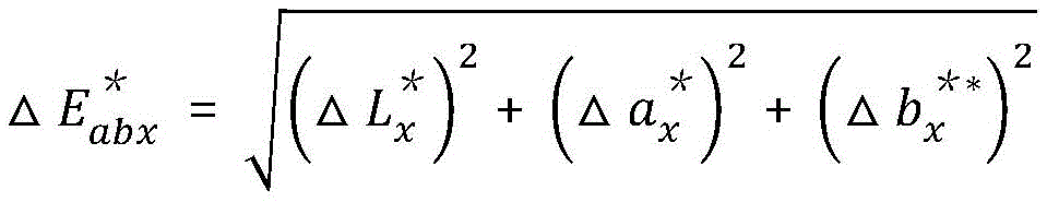
l for measured N +1 points*Value a*Value b and*the values are respectively subjected to difference operation to obtain delta L*Value Δ a*Value sum Δ b*Value, pair DeltaL*Value Δ a*Value sum Deltab*Respectively squaring the sum value, calculating the square root of the sum value, and calculating the uniformity of chromatic aberration of the wafer based on the square root result
L for measured N +1 points*The difference value is calculated to obtain delta L*Value based on Δ L*Value-calculating chromatic aberration uniformity of wafer
Algorithm 1: calculating the color difference uniformity of the wafer based on the square root result The method comprises the following specific steps:


wherein, l representing measured N +1 points*The maximum value of the values;
 l representing measured N +1 points*A minimum value of the value;
 a representing measured N +1 points*The maximum value of the value;
 a representing measured N +1 points*A minimum value of the value;
 b representing measured N +1 points*The maximum value of the value;
 b representing measured N +1 points*The minimum value of the values.
△L*A positive value indicates a white bias,. DELTA.L*Negative values indicate a partial darkness; delta a*A positive value indicates a red bias, Δ a*A negative value indicates greenish; delta b*A positive value indicates a yellowish color,. DELTA.b*Negative values indicate bluish.
An example of the calculation of the 5 measurement points is shown in table 2 below.
TABLE 2


In the table, L*Value a*Value b and b*Values were measured by spectrocolorimeter at 5 points according to figure 1; according to the formula
 Calculated, in
 algorithm 1, calculated Only one; l is*Average value of L of 5 points*The average value of the values (wafer colorimetric value) was calculated
 L*Mean =48.42, chroma type 3A of the LT crystal substrate.
The correspondence between the wafer colorimetric values and the chromaticity types (color depth after wafer blackening) is shown in table 3 below.
TABLE 3

And 2, algorithm: calculating the color difference uniformity of the wafer based on the square root result The method comprises the following specific steps:


wherein, l representing the measured center point*A value;
 indicating measurementsL of the x-th point of a predetermined distance from the edge of the wafer*Value, x ∈ [2, N +1];
 A representing the measured center point*A value;
 a representing the measured x-th point a preset distance from the edge of the wafer*A value;
 b representing the measured center point*A value;
 b representing the x-th point of the measured preset distance from the edge of the wafer*A value;
obtaining the calculated N Maximum value of (1) as uniformity of color difference Δ E* abOr, for the calculated N
 Taking the average value as the color difference uniformity
The following Table 4,L*Value a*Value b and*values were measured by spectrocolorimeter according to 5 points of fig. 1. In the algorithm, a total of 4 are calculated
An example of the calculation of the 5 measurement points is shown in table 4 below.
TABLE 4

In the table, L*Value a*Value b and*values were measured by spectrocolorimeter at 5 points as in figure 1; in the present algorithm 2, calculated There are four of the number of the first,
 take the calculated 4
 Maximum value of (1); l is*Average value of L of 5 points*The average value of the values (wafer colorimetric value) was calculated
 L x mean =48.42, the LT crystal substrate has a chromaticity type 3A.
And (3) algorithm: calculating the color difference uniformity of the wafer based on the square root result The method comprises the following specific steps:


wherein, l representing the measured z-th point*A value;
 l representing measured N other points excluding the z-th point*Value, z ∈ [1, N +1],
 And is not equal to z, y ∈ [1, N (N + 1)/2];
 A representing the measured z-th point*A value;
 a representing measured other N points excluding the z-th point*A value;
 b representing the measured z-th point*A value;
 b representing measured N other points excluding the z-th point*A value;
obtaining the calculated N (N + 1)/2 Maximum value of (1) as uniformity of color difference
 Or, for the calculated N (N + 1)/2
 Taking the average value as the color difference uniformity
The following Table 5,L*Value a*Value b and*values were measured by spectrocolorimeter according to 5 points of figure 1. In this algorithm, N (N + 1)/2 (10 pieces) are calculated in total
A calculation example of 5 measurement points is shown in table 5 below.
TABLE 5

In the table, L*Value a*Value b and*values were measured by spectrocolorimeter at 5 points according to figure 1; in the present algorithm 3, calculated There are 10 of them, and the number of them,
 taking the calculated 10
 Maximum value of (2); l is*Average value of L of 5 points*The average value of the values (wafer colorimetric value) was calculated
 L*Average =48.42, the LT crystal substrate is of chroma type 3A.
And algorithm 4: based on Delta L*Value calculation for wafer color difference uniformity The method comprises the following specific steps:

wherein, l representing measured N +1 points*The maximum value of the value;
 l representing N +1 points measured*The minimum value of the values.
An example of the calculation of the 5 measurement points is shown in table 6 below.
TABLE 6

In the table, L*Value a*Value b and b*Values were measured by spectrocolorimeter at 5 points according to figure 1; in this algorithm 4, calculated Only one, equal to 0.44, L*Average =48.42, the LT crystal substrate is of chroma type 3A.
Referring to FIG. 3, the calculated color difference uniformity is shown when measuring 100 doped wafers (AlTa + Fe) according to an embodiment of the present invention A comparative schematic of the four algorithms of (a). The graph is a related scatter diagram, and is obtained by taking an
 algorithm 1 as an abscissa and taking an algorithm 2, an algorithm 3 and an algorithm 4 as ordinates respectively. As can be seen from the figure, by comparing four different calculation modes, the average difference of the uniformity of algorithm 1, algorithm 2 and algorithm 3 is 0.027, and the correlation R2=0.9941 is higher than that, and is highly linear; the correlation R2=0.9781 for algorithm 1 and algorithm 4 is highly linear, but the deviation is larger than for the other three algorithms (in CIE LAB, a)*,b*Influence).
Referring to FIG. 4, the calculated color difference uniformity is shown when measuring 100 undoped wafers (AlTa) according to an embodiment of the present invention A comparative schematic of the four algorithms of (a). The graph is a related scatter diagram, and is obtained by taking an
 algorithm 1 as an abscissa and taking an algorithm 2, an algorithm 3 and an algorithm 4 as ordinates respectively. As can be seen from the figure, the correlation result, the correlation R, is obtained by comparing four different calculation modes2Is more than 0.9915, has high linear correlation (the white and black sheets are not doped and are not subjected to a)*,b*Influence).
In summary, since the current mainstream product is a doped wafer, and the algorithm 2 is suitable for doped and undoped wafers, the algorithm 2 has wider applicability; calculating L Using Algorithm 3*The calculation logic is long and complicated (N (N + 1)/2 values are required to be calculated); the algorithm 2 is more in accordance with the CIE15 definition, so that the algorithm 2 is preferably selected to calculate the uniformity of chromatic aberration in practical use
Referring to fig. 5, a method for obtaining a reduction blackening color of a wafer in this embodiment further includes:
s103, judging the line width uniformity of the wafer based on the color difference uniformity;
s104, measuring L of N +1 points*Taking the average value as the wafer chromatic value;
and S105, judging the transmittance of the wafer based on the wafer colorimetric value.
In an embodiment, determining the line width uniformity of the wafer based on the color difference uniformity specifically includes:
and comparing the calculated color difference uniformity with a preset uniformity category, judging the uniformity category to which the color difference uniformity belongs, and judging the line width uniformity of the wafer according to the uniformity category to which the color difference uniformity belongs.
Referring to fig. 6 and 7, in another embodiment, the calculated color difference uniformity is substituted into the fitted color difference-line width linear equation to calculate the color difference uniformity corresponding to the color difference uniformity.
In fig. 7, the linear equation of the chromatic aberration-line width of the doped wafer is y =87.153x-0.0715. Wherein x represents line width uniformity CD and y represents color difference uniformity And calculating the color difference uniformity of the wafer by using the color difference uniformity through the fitted linear equation, and quickly and accurately calculating the color difference uniformity of the wafer so as to judge the exposure yield of the back-stage yellow light process.
It should be noted that the above linear equation is only a schematic equation, and the coefficients of the above linear equation may change to some extent as the measured data increases or the fitting manner changes.
In one embodiment, determining the transmittance of the wafer based on the wafer colorimetric values specifically includes:
comparing the calculated wafer colorimetric values with preset colorimetric categories, determining the colorimetric categories to which the wafer colorimetric values belong, and determining the transmittance of the wafer according to the colorimetric categories to which the wafer colorimetric values belong, which is specifically shown in table 2 above. The transmittance of the wafer is judged according to the color class, and the method belongs to a qualitative analysis method and can quickly and roughly judge whether the transmittance meets the requirements of customers.
Referring to fig. 8, in another embodiment, the determining the transmittance of the wafer based on the wafer colorimetric values specifically includes:
and substituting the calculated wafer colorimetric values into the fitted chromaticity-transmittance linear equation to calculate the transmittance corresponding to the wafer colorimetric values.
In fig. 8, the chromaticity-transmittance linear equation of the doped wafer is given as y =0.0229x-0.7692, and the chromaticity-transmittance linear equation of the undoped wafer is given as y =0.0648x-2.5688. Wherein x represents L*The average value, y, represents the transmittance. Wherein LT denotes an undoped lithium tantalate wafer, and LT (Fe) denotes an Fe-doped lithium tantalate wafer. Using the wafer by fitting a linear equationThe transmittance of the wafer is calculated by the chromatic value, and the method belongs to a quantitative analysis method, and can quickly and accurately calculate the transmittance, so as to judge whether the transmittance meets the requirements of customers.
It should be noted that the linear equation is only a schematic equation, and the coefficients of the linear equation may change to some extent as the measured data increases or the fitting manner changes.
As can be seen from FIG. 8, the measured LT wafer chromaticity categories 0A, 1A, 2A, 3A, SB2 have strong correlation with respect to transmittance at wavelengths of 200nm to 700 nm.
In conclusion, the embodiment can calculate the uniformity of wafer chromatic aberration and the chromatic value of the wafer, and further monitor the transmittance through the uniformity of the chromaticity and the chromatic aberration of the LT crystal substrate, thereby avoiding the follow current of the wafer operation process which is not compliant, instantly knowing whether the transmittance of the blackened crystal meets the requirements of customers, avoiding the transmittance which can be measured through long-process operation to double-side polishing, reducing the waste and loss of materials and manpower, instantly monitoring the quality of the transmittance of the product, greatly saving the cost of the product, and having very good yield of the integrated circuit yellow light process.
Referring to fig. 9, a wafer reduction blackening color acquisition system includes:
a data acquisition module 901 for measuring the center point of the wafer and L of N points at a predetermined distance from the edge of the wafer*Value a*Value b and*a value; the N points are uniformly distributed along the circumferential direction of the wafer; l is a radical of an alcohol*The value represents the magnitude of the chromaticity value of the point; a is a*The value represents the red-green degree of the point; b*The value represents the degree of yellow-blue of the dot;
a color difference uniformity obtaining module 902, configured to measure L of N +1 points*Performing difference operation on the values or measuring L of N +1 points*Value a*Value b and*performing difference operation on the values respectively, and calculating the color difference uniformity of the wafer based on the result of the difference operation;
a line width uniformity judging module 903, configured to judge line width uniformity of the wafer based on the color difference uniformity;
a wafer colorimetric value obtaining module 904 for obtaining L of the measured N +1 point*Taking the average value as the wafer chromatic value;
and the transmittance judging module 905 is used for judging the transmittance of the wafer based on the wafer colorimetric value.
A method for acquiring a reduced blackened color of a wafer by a system for acquiring a reduced blackened color of a wafer is provided, and the embodiment is not repeated.
The foregoing is only a preferred embodiment of the present invention, and it should be noted that modifications can be made by those skilled in the art without departing from the principle of the present invention, and these modifications should also be construed as the protection scope of the present invention.
Claims (10)
1. A method for obtaining a reduction blackening color of a wafer is characterized by comprising the following steps:
measuring L of the center point of the wafer and N points at a preset distance from the edge of the wafer*Value a*Value b and*a value; the N points are uniformly distributed along the circumferential direction of the wafer; l is a radical of an alcohol*The value represents the magnitude of the chromaticity value of the point; a is*The value represents the red-green degree of the point; b is a mixture of*The value represents the degree of yellow-blue of the dot;
l for measured N +1 points*Performing difference operation on the values or measuring L of N +1 points*Value a*Value b and*and respectively carrying out difference operation on the values, and calculating the color difference uniformity of the wafer based on the result of the difference operation.
2. The method as claimed in claim 1, wherein L is measured at N +1 points*Value a*Value b and*and respectively carrying out difference operation on the values, and calculating the color difference uniformity of the wafer based on the result of the difference operation, wherein the method specifically comprises the following steps:
l for measured N +1 points*Value a*Value b and b*Value divisionRespectively performing difference operation to obtain delta L*Value Δ a*Value sum Deltab*Value, pair DeltaL*Value Δ a*Value sum Deltab*Respectively squaring the sum, calculating the square root of the sum, and calculating the uniformity of chromatic aberration of the wafer based on the result of the square root
3. The method as claimed in claim 2, wherein the color difference uniformity of the wafer is calculated based on the square root result The method comprises the following specific steps:


wherein, l representing N +1 points measured*The maximum value of the value;
 l representing measured N +1 points*A minimum value of the value;
 a representing measured N +1 points*The maximum value of the value;
 a representing measured N +1 points*A minimum value of the value;
 b representing measured N +1 points*The maximum value of the values;
 b representing measured N +1 points*The minimum value of the values.
4. The method as claimed in claim 2, wherein the color difference uniformity of the wafer is calculated based on the square root result The method comprises the following specific steps:


wherein, l representing the measured center point*A value;
 l representing the x-th point of the measured preset distance from the edge of the wafer*Value, x ∈ [2, N +1];
 A representing the measured center point*A value;
 a representing the x-th point of the measured preset distance from the edge of the wafer*A value;
 b representing the measured center point*A value;
 b representing the x-th point of the measured preset distance from the edge of the wafer*A value;
obtaining the calculated N Maximum value of (1) as uniformity of color difference Δ E* abOr, for the calculated N
 Taking the average as the uniformity of chromatic aberration
5. The method as claimed in claim 2, wherein the color difference uniformity of the wafer is calculated based on the square root result The method comprises the following specific steps:


wherein, l representing the measured z-th point*A value;
 l representing other N measured points not including the z-th point*Value, z ∈ [1, N +1],
 And is not equal to z, y ∈ [1, N (N + 1)/2];
 A representing the measured z-th point*A value;
 a representing measured other N points excluding the z-th point*A value;
 b representing the measured z-th point*A value;
 b representing measured other N points excluding the z-th point*A value;
obtaining the calculated N (N + 1)/2 Maximum value of (1) as uniformity of color difference
 Or, for the calculated N (N + 1)/2
 Taking the average as the uniformity of chromatic aberration
6. The wafer reduction blackening color obtaining method as recited in claim 1, wherein L is measured for N +1 points*Performing difference operation on the values, and calculating the color difference uniformity of the wafer based on the result of the difference operation, wherein the method specifically comprises the following steps:
l for measured N +1 points*The difference value is calculated to obtain Delta L*Value based on Δ L*Value-calculating chromatic aberration uniformity of wafer
7. The method as claimed in claim 6, wherein the color of the black image is obtained based on Δ L*Value-calculating chromatic aberration uniformity of wafer The method comprises the following specific steps:

wherein, l representing measured N +1 points*The maximum value of the values;
 l representing measured N +1 points*The minimum value of the values.
8. The method for acquiring reduction blackening color of a wafer according to claim 1, further comprising: judging the line width uniformity of the wafer based on the color difference uniformity;
the method specifically comprises the following steps:
comparing the calculated color difference uniformity with a preset uniformity category, judging the uniformity category to which the color difference uniformity belongs, and judging the line width uniformity of the wafer according to the uniformity category to which the color difference uniformity belongs;
or,
and substituting the calculated color difference uniformity into the fitted color difference-line width linear equation to calculate the line width uniformity corresponding to the color difference uniformity.
9. The method for acquiring reduction blackening color of a wafer according to claim 1, further comprising:
l for measured N +1 points*Taking the average value as the wafer chromatic value; judging the transmittance of the wafer based on the wafer colorimetric value;
judging the transmittance of the wafer based on the wafer colorimetric value specifically comprises the following steps:
comparing the calculated wafer colorimetric value with a preset colorimetric category, judging the colorimetric category to which the wafer colorimetric value belongs, and judging the transmittance of the wafer according to the belonging colorimetric category;
or,
and substituting the calculated wafer colorimetric values into the fitted chromaticity-transmittance linear equation to calculate the transmittance corresponding to the wafer colorimetric values.
10. A wafer reduction blackening color acquisition system, comprising:
a data acquisition module for measuring the center point of the wafer and L of N points at a preset distance from the edge of the wafer*Value a*Value b and*a value; the N points are uniformly distributed along the circumferential direction of the wafer; l is a radical of an alcohol*The value represents the magnitude of the chromaticity value of the point; a is*The value represents the red-green degree of the point; b*The value represents the degree of yellow-blue of the dot;
a color difference uniformity obtaining module for measuring L of N +1 points*Performing difference operation on the values or measuring L of N +1 points*Value a*Value b and*performing difference operation on the values respectively, and calculating the color difference uniformity of the wafer based on the result of the difference operation;
the line width uniformity judging module is used for judging the line width uniformity of the wafer based on the color difference uniformity;
a wafer colorimetric value acquisition module for measuring L of N +1 points*Taking the average value of the values as the wafer chromatic value;
and the transmittance judging module is used for judging the transmittance of the wafer based on the wafer colorimetric value.
Priority Applications (1)
| Application Number | Priority Date | Filing Date | Title |
|---|---|---|---|
| CN202210758853.6A CN115270051A (en) | 2022-06-30 | 2022-06-30 | Method and system for obtaining reduced blackening color of wafer |
Applications Claiming Priority (1)
| Application Number | Priority Date | Filing Date | Title |
|---|---|---|---|
| CN202210758853.6A CN115270051A (en) | 2022-06-30 | 2022-06-30 | Method and system for obtaining reduced blackening color of wafer |
Publications (1)
| Publication Number | Publication Date |
|---|---|
| CN115270051A true CN115270051A (en) | 2022-11-01 |
Family
ID=83763386
Family Applications (1)
| Application Number | Title | Priority Date | Filing Date |
|---|---|---|---|
| CN202210758853.6A Withdrawn CN115270051A (en) | 2022-06-30 | 2022-06-30 | Method and system for obtaining reduced blackening color of wafer |
Country Status (1)
| Country | Link |
|---|---|
| CN (1) | CN115270051A (en) |
Cited By (1)
| Publication number | Priority date | Publication date | Assignee | Title |
|---|---|---|---|---|
| CN117197129A (en) * | 2023-11-03 | 2023-12-08 | 浙江鑫柔科技有限公司 | Blackening degree detection method and device and computer equipment |
-
2022
- 2022-06-30 CN CN202210758853.6A patent/CN115270051A/en not_active Withdrawn
Cited By (2)
| Publication number | Priority date | Publication date | Assignee | Title |
|---|---|---|---|---|
| CN117197129A (en) * | 2023-11-03 | 2023-12-08 | 浙江鑫柔科技有限公司 | Blackening degree detection method and device and computer equipment |
| CN117197129B (en) * | 2023-11-03 | 2024-02-13 | 浙江鑫柔科技有限公司 | Blackening degree detection method and device and computer equipment |
Similar Documents
| Publication | Publication Date | Title |
|---|---|---|
| US6750976B2 (en) | Device for manufacturing semiconductor device and method of manufacturing the same | |
| US5939886A (en) | Plasma monitoring and control method and system | |
| US5405488A (en) | System and method for plasma etching endpoint detection | |
| US20080020495A1 (en) | Semiconductor fabricating apparatus with function of determining etching processing state | |
| JP4267575B2 (en) | Method and apparatus for determining etch characteristics using endpoint signals | |
| CN115270051A (en) | Method and system for obtaining reduced blackening color of wafer | |
| CN115790412B (en) | Film thickness test and uniformity adjustment method | |
| US6594025B2 (en) | Method of monitoring thin-film processes and metrology tool thereof | |
| KR100938947B1 (en) | Apparatus and method for endpoint detection | |
| US20110215072A1 (en) | Plasma apparatus having a controller for controlling a plasma chamber and methods for controlling the plasma apparatus | |
| EP0454499B1 (en) | Method for evaluating a lithium niobate thin film and apparatus for preparing the same | |
| US20070178610A1 (en) | Semiconductor Production Apparatus | |
| CN101958242A (en) | Method for manufacturing gate oxide layer and grid polycrystalline silicon layer | |
| CN106876236A (en) | The apparatus and method for monitoring plasma process processing procedure | |
| KR100945889B1 (en) | Determination Method of Plasma Treatment | |
| KR20060085247A (en) | Impurity introduction method, impurity introduction device, and electronic device formed using them | |
| CN110190827B (en) | A method for ion beam frequency modulation based on surface acoustic wave | |
| TW202338952A (en) | Method for cleaning silicon wafer and method for manufacturing silicon wafer with natural oxide film | |
| CN100361278C (en) | Method for judging semiconductor manufacturing process state and semiconductor manufacturing device | |
| CN106876238A (en) | The apparatus and method for monitoring plasma process processing procedure | |
| Kim et al. | Impedance monitoring of a plasma chamber under plasma-off conditions for contamination control | |
| KR100902365B1 (en) | Semiconductor manufacturing device | |
| TW559941B (en) | Manufacturing apparatus of semiconductor and judging method of end point | |
| CN110660697A (en) | Method and device for determining process parameters of mercury cadmium telluride passivation film | |
| CN117812986A (en) | Piezoelectric wafer, method for manufacturing the same, and elastic wave device |
Legal Events
| Date | Code | Title | Description |
|---|---|---|---|
| PB01 | Publication | ||
| PB01 | Publication | ||
| SE01 | Entry into force of request for substantive examination | ||
| SE01 | Entry into force of request for substantive examination | ||
| WW01 | Invention patent application withdrawn after publication |
Application publication date: 20221101 |
|
| WW01 | Invention patent application withdrawn after publication |