CN115202115A - Display device - Google Patents
Display device Download PDFInfo
- Publication number
- CN115202115A CN115202115A CN202210844141.6A CN202210844141A CN115202115A CN 115202115 A CN115202115 A CN 115202115A CN 202210844141 A CN202210844141 A CN 202210844141A CN 115202115 A CN115202115 A CN 115202115A
- Authority
- CN
- China
- Prior art keywords
- transistor
- wiring
- electrode
- pixel
- light
- Prior art date
- Legal status (The legal status is an assumption and is not a legal conclusion. Google has not performed a legal analysis and makes no representation as to the accuracy of the status listed.)
- Granted
Links
Images


Classifications
-
- G—PHYSICS
- G02—OPTICS
- G02F—OPTICAL DEVICES OR ARRANGEMENTS FOR THE CONTROL OF LIGHT BY MODIFICATION OF THE OPTICAL PROPERTIES OF THE MEDIA OF THE ELEMENTS INVOLVED THEREIN; NON-LINEAR OPTICS; FREQUENCY-CHANGING OF LIGHT; OPTICAL LOGIC ELEMENTS; OPTICAL ANALOGUE/DIGITAL CONVERTERS
- G02F1/00—Devices or arrangements for the control of the intensity, colour, phase, polarisation or direction of light arriving from an independent light source, e.g. switching, gating or modulating; Non-linear optics
- G02F1/01—Devices or arrangements for the control of the intensity, colour, phase, polarisation or direction of light arriving from an independent light source, e.g. switching, gating or modulating; Non-linear optics for the control of the intensity, phase, polarisation or colour
- G02F1/13—Devices or arrangements for the control of the intensity, colour, phase, polarisation or direction of light arriving from an independent light source, e.g. switching, gating or modulating; Non-linear optics for the control of the intensity, phase, polarisation or colour based on liquid crystals, e.g. single liquid crystal display cells
- G02F1/133—Constructional arrangements; Operation of liquid crystal cells; Circuit arrangements
- G02F1/136—Liquid crystal cells structurally associated with a semi-conducting layer or substrate, e.g. cells forming part of an integrated circuit
- G02F1/1362—Active matrix addressed cells
- G02F1/136286—Wiring, e.g. gate line, drain line
-
- G—PHYSICS
- G02—OPTICS
- G02F—OPTICAL DEVICES OR ARRANGEMENTS FOR THE CONTROL OF LIGHT BY MODIFICATION OF THE OPTICAL PROPERTIES OF THE MEDIA OF THE ELEMENTS INVOLVED THEREIN; NON-LINEAR OPTICS; FREQUENCY-CHANGING OF LIGHT; OPTICAL LOGIC ELEMENTS; OPTICAL ANALOGUE/DIGITAL CONVERTERS
- G02F1/00—Devices or arrangements for the control of the intensity, colour, phase, polarisation or direction of light arriving from an independent light source, e.g. switching, gating or modulating; Non-linear optics
- G02F1/01—Devices or arrangements for the control of the intensity, colour, phase, polarisation or direction of light arriving from an independent light source, e.g. switching, gating or modulating; Non-linear optics for the control of the intensity, phase, polarisation or colour
- G02F1/13—Devices or arrangements for the control of the intensity, colour, phase, polarisation or direction of light arriving from an independent light source, e.g. switching, gating or modulating; Non-linear optics for the control of the intensity, phase, polarisation or colour based on liquid crystals, e.g. single liquid crystal display cells
- G02F1/133—Constructional arrangements; Operation of liquid crystal cells; Circuit arrangements
- G02F1/136—Liquid crystal cells structurally associated with a semi-conducting layer or substrate, e.g. cells forming part of an integrated circuit
- G02F1/1362—Active matrix addressed cells
- G02F1/136213—Storage capacitors associated with the pixel electrode
-
- G—PHYSICS
- G02—OPTICS
- G02F—OPTICAL DEVICES OR ARRANGEMENTS FOR THE CONTROL OF LIGHT BY MODIFICATION OF THE OPTICAL PROPERTIES OF THE MEDIA OF THE ELEMENTS INVOLVED THEREIN; NON-LINEAR OPTICS; FREQUENCY-CHANGING OF LIGHT; OPTICAL LOGIC ELEMENTS; OPTICAL ANALOGUE/DIGITAL CONVERTERS
- G02F1/00—Devices or arrangements for the control of the intensity, colour, phase, polarisation or direction of light arriving from an independent light source, e.g. switching, gating or modulating; Non-linear optics
- G02F1/01—Devices or arrangements for the control of the intensity, colour, phase, polarisation or direction of light arriving from an independent light source, e.g. switching, gating or modulating; Non-linear optics for the control of the intensity, phase, polarisation or colour
- G02F1/13—Devices or arrangements for the control of the intensity, colour, phase, polarisation or direction of light arriving from an independent light source, e.g. switching, gating or modulating; Non-linear optics for the control of the intensity, phase, polarisation or colour based on liquid crystals, e.g. single liquid crystal display cells
- G02F1/133—Constructional arrangements; Operation of liquid crystal cells; Circuit arrangements
- G02F1/136—Liquid crystal cells structurally associated with a semi-conducting layer or substrate, e.g. cells forming part of an integrated circuit
- G02F1/1362—Active matrix addressed cells
- G02F1/13624—Active matrix addressed cells having more than one switching element per pixel
-
- G—PHYSICS
- G02—OPTICS
- G02F—OPTICAL DEVICES OR ARRANGEMENTS FOR THE CONTROL OF LIGHT BY MODIFICATION OF THE OPTICAL PROPERTIES OF THE MEDIA OF THE ELEMENTS INVOLVED THEREIN; NON-LINEAR OPTICS; FREQUENCY-CHANGING OF LIGHT; OPTICAL LOGIC ELEMENTS; OPTICAL ANALOGUE/DIGITAL CONVERTERS
- G02F1/00—Devices or arrangements for the control of the intensity, colour, phase, polarisation or direction of light arriving from an independent light source, e.g. switching, gating or modulating; Non-linear optics
- G02F1/01—Devices or arrangements for the control of the intensity, colour, phase, polarisation or direction of light arriving from an independent light source, e.g. switching, gating or modulating; Non-linear optics for the control of the intensity, phase, polarisation or colour
- G02F1/13—Devices or arrangements for the control of the intensity, colour, phase, polarisation or direction of light arriving from an independent light source, e.g. switching, gating or modulating; Non-linear optics for the control of the intensity, phase, polarisation or colour based on liquid crystals, e.g. single liquid crystal display cells
- G02F1/133—Constructional arrangements; Operation of liquid crystal cells; Circuit arrangements
- G02F1/136—Liquid crystal cells structurally associated with a semi-conducting layer or substrate, e.g. cells forming part of an integrated circuit
- G02F1/1362—Active matrix addressed cells
- G02F1/1368—Active matrix addressed cells in which the switching element is a three-electrode device
-
- G—PHYSICS
- G09—EDUCATION; CRYPTOGRAPHY; DISPLAY; ADVERTISING; SEALS
- G09G—ARRANGEMENTS OR CIRCUITS FOR CONTROL OF INDICATING DEVICES USING STATIC MEANS TO PRESENT VARIABLE INFORMATION
- G09G3/00—Control arrangements or circuits, of interest only in connection with visual indicators other than cathode-ray tubes
- G09G3/20—Control arrangements or circuits, of interest only in connection with visual indicators other than cathode-ray tubes for presentation of an assembly of a number of characters, e.g. a page, by composing the assembly by combination of individual elements arranged in a matrix no fixed position being assigned to or needed to be assigned to the individual characters or partial characters
- G09G3/22—Control arrangements or circuits, of interest only in connection with visual indicators other than cathode-ray tubes for presentation of an assembly of a number of characters, e.g. a page, by composing the assembly by combination of individual elements arranged in a matrix no fixed position being assigned to or needed to be assigned to the individual characters or partial characters using controlled light sources
- G09G3/30—Control arrangements or circuits, of interest only in connection with visual indicators other than cathode-ray tubes for presentation of an assembly of a number of characters, e.g. a page, by composing the assembly by combination of individual elements arranged in a matrix no fixed position being assigned to or needed to be assigned to the individual characters or partial characters using controlled light sources using electroluminescent panels
- G09G3/32—Control arrangements or circuits, of interest only in connection with visual indicators other than cathode-ray tubes for presentation of an assembly of a number of characters, e.g. a page, by composing the assembly by combination of individual elements arranged in a matrix no fixed position being assigned to or needed to be assigned to the individual characters or partial characters using controlled light sources using electroluminescent panels semiconductive, e.g. using light-emitting diodes [LED]
- G09G3/3208—Control arrangements or circuits, of interest only in connection with visual indicators other than cathode-ray tubes for presentation of an assembly of a number of characters, e.g. a page, by composing the assembly by combination of individual elements arranged in a matrix no fixed position being assigned to or needed to be assigned to the individual characters or partial characters using controlled light sources using electroluminescent panels semiconductive, e.g. using light-emitting diodes [LED] organic, e.g. using organic light-emitting diodes [OLED]
- G09G3/3225—Control arrangements or circuits, of interest only in connection with visual indicators other than cathode-ray tubes for presentation of an assembly of a number of characters, e.g. a page, by composing the assembly by combination of individual elements arranged in a matrix no fixed position being assigned to or needed to be assigned to the individual characters or partial characters using controlled light sources using electroluminescent panels semiconductive, e.g. using light-emitting diodes [LED] organic, e.g. using organic light-emitting diodes [OLED] using an active matrix
- G09G3/3233—Control arrangements or circuits, of interest only in connection with visual indicators other than cathode-ray tubes for presentation of an assembly of a number of characters, e.g. a page, by composing the assembly by combination of individual elements arranged in a matrix no fixed position being assigned to or needed to be assigned to the individual characters or partial characters using controlled light sources using electroluminescent panels semiconductive, e.g. using light-emitting diodes [LED] organic, e.g. using organic light-emitting diodes [OLED] using an active matrix with pixel circuitry controlling the current through the light-emitting element
-
- G—PHYSICS
- G09—EDUCATION; CRYPTOGRAPHY; DISPLAY; ADVERTISING; SEALS
- G09G—ARRANGEMENTS OR CIRCUITS FOR CONTROL OF INDICATING DEVICES USING STATIC MEANS TO PRESENT VARIABLE INFORMATION
- G09G3/00—Control arrangements or circuits, of interest only in connection with visual indicators other than cathode-ray tubes
- G09G3/20—Control arrangements or circuits, of interest only in connection with visual indicators other than cathode-ray tubes for presentation of an assembly of a number of characters, e.g. a page, by composing the assembly by combination of individual elements arranged in a matrix no fixed position being assigned to or needed to be assigned to the individual characters or partial characters
- G09G3/22—Control arrangements or circuits, of interest only in connection with visual indicators other than cathode-ray tubes for presentation of an assembly of a number of characters, e.g. a page, by composing the assembly by combination of individual elements arranged in a matrix no fixed position being assigned to or needed to be assigned to the individual characters or partial characters using controlled light sources
- G09G3/30—Control arrangements or circuits, of interest only in connection with visual indicators other than cathode-ray tubes for presentation of an assembly of a number of characters, e.g. a page, by composing the assembly by combination of individual elements arranged in a matrix no fixed position being assigned to or needed to be assigned to the individual characters or partial characters using controlled light sources using electroluminescent panels
- G09G3/32—Control arrangements or circuits, of interest only in connection with visual indicators other than cathode-ray tubes for presentation of an assembly of a number of characters, e.g. a page, by composing the assembly by combination of individual elements arranged in a matrix no fixed position being assigned to or needed to be assigned to the individual characters or partial characters using controlled light sources using electroluminescent panels semiconductive, e.g. using light-emitting diodes [LED]
- G09G3/3208—Control arrangements or circuits, of interest only in connection with visual indicators other than cathode-ray tubes for presentation of an assembly of a number of characters, e.g. a page, by composing the assembly by combination of individual elements arranged in a matrix no fixed position being assigned to or needed to be assigned to the individual characters or partial characters using controlled light sources using electroluminescent panels semiconductive, e.g. using light-emitting diodes [LED] organic, e.g. using organic light-emitting diodes [OLED]
- G09G3/3266—Details of drivers for scan electrodes
-
- G—PHYSICS
- G09—EDUCATION; CRYPTOGRAPHY; DISPLAY; ADVERTISING; SEALS
- G09G—ARRANGEMENTS OR CIRCUITS FOR CONTROL OF INDICATING DEVICES USING STATIC MEANS TO PRESENT VARIABLE INFORMATION
- G09G3/00—Control arrangements or circuits, of interest only in connection with visual indicators other than cathode-ray tubes
- G09G3/20—Control arrangements or circuits, of interest only in connection with visual indicators other than cathode-ray tubes for presentation of an assembly of a number of characters, e.g. a page, by composing the assembly by combination of individual elements arranged in a matrix no fixed position being assigned to or needed to be assigned to the individual characters or partial characters
- G09G3/22—Control arrangements or circuits, of interest only in connection with visual indicators other than cathode-ray tubes for presentation of an assembly of a number of characters, e.g. a page, by composing the assembly by combination of individual elements arranged in a matrix no fixed position being assigned to or needed to be assigned to the individual characters or partial characters using controlled light sources
- G09G3/30—Control arrangements or circuits, of interest only in connection with visual indicators other than cathode-ray tubes for presentation of an assembly of a number of characters, e.g. a page, by composing the assembly by combination of individual elements arranged in a matrix no fixed position being assigned to or needed to be assigned to the individual characters or partial characters using controlled light sources using electroluminescent panels
- G09G3/32—Control arrangements or circuits, of interest only in connection with visual indicators other than cathode-ray tubes for presentation of an assembly of a number of characters, e.g. a page, by composing the assembly by combination of individual elements arranged in a matrix no fixed position being assigned to or needed to be assigned to the individual characters or partial characters using controlled light sources using electroluminescent panels semiconductive, e.g. using light-emitting diodes [LED]
- G09G3/3208—Control arrangements or circuits, of interest only in connection with visual indicators other than cathode-ray tubes for presentation of an assembly of a number of characters, e.g. a page, by composing the assembly by combination of individual elements arranged in a matrix no fixed position being assigned to or needed to be assigned to the individual characters or partial characters using controlled light sources using electroluminescent panels semiconductive, e.g. using light-emitting diodes [LED] organic, e.g. using organic light-emitting diodes [OLED]
- G09G3/3275—Details of drivers for data electrodes
-
- G—PHYSICS
- G09—EDUCATION; CRYPTOGRAPHY; DISPLAY; ADVERTISING; SEALS
- G09G—ARRANGEMENTS OR CIRCUITS FOR CONTROL OF INDICATING DEVICES USING STATIC MEANS TO PRESENT VARIABLE INFORMATION
- G09G3/00—Control arrangements or circuits, of interest only in connection with visual indicators other than cathode-ray tubes
- G09G3/20—Control arrangements or circuits, of interest only in connection with visual indicators other than cathode-ray tubes for presentation of an assembly of a number of characters, e.g. a page, by composing the assembly by combination of individual elements arranged in a matrix no fixed position being assigned to or needed to be assigned to the individual characters or partial characters
- G09G3/34—Control arrangements or circuits, of interest only in connection with visual indicators other than cathode-ray tubes for presentation of an assembly of a number of characters, e.g. a page, by composing the assembly by combination of individual elements arranged in a matrix no fixed position being assigned to or needed to be assigned to the individual characters or partial characters by control of light from an independent source
- G09G3/3406—Control of illumination source
- G09G3/3413—Details of control of colour illumination sources
-
- G—PHYSICS
- G09—EDUCATION; CRYPTOGRAPHY; DISPLAY; ADVERTISING; SEALS
- G09G—ARRANGEMENTS OR CIRCUITS FOR CONTROL OF INDICATING DEVICES USING STATIC MEANS TO PRESENT VARIABLE INFORMATION
- G09G3/00—Control arrangements or circuits, of interest only in connection with visual indicators other than cathode-ray tubes
- G09G3/20—Control arrangements or circuits, of interest only in connection with visual indicators other than cathode-ray tubes for presentation of an assembly of a number of characters, e.g. a page, by composing the assembly by combination of individual elements arranged in a matrix no fixed position being assigned to or needed to be assigned to the individual characters or partial characters
- G09G3/34—Control arrangements or circuits, of interest only in connection with visual indicators other than cathode-ray tubes for presentation of an assembly of a number of characters, e.g. a page, by composing the assembly by combination of individual elements arranged in a matrix no fixed position being assigned to or needed to be assigned to the individual characters or partial characters by control of light from an independent source
- G09G3/36—Control arrangements or circuits, of interest only in connection with visual indicators other than cathode-ray tubes for presentation of an assembly of a number of characters, e.g. a page, by composing the assembly by combination of individual elements arranged in a matrix no fixed position being assigned to or needed to be assigned to the individual characters or partial characters by control of light from an independent source using liquid crystals
- G09G3/3611—Control of matrices with row and column drivers
- G09G3/3648—Control of matrices with row and column drivers using an active matrix
-
- G—PHYSICS
- G09—EDUCATION; CRYPTOGRAPHY; DISPLAY; ADVERTISING; SEALS
- G09G—ARRANGEMENTS OR CIRCUITS FOR CONTROL OF INDICATING DEVICES USING STATIC MEANS TO PRESENT VARIABLE INFORMATION
- G09G3/00—Control arrangements or circuits, of interest only in connection with visual indicators other than cathode-ray tubes
- G09G3/20—Control arrangements or circuits, of interest only in connection with visual indicators other than cathode-ray tubes for presentation of an assembly of a number of characters, e.g. a page, by composing the assembly by combination of individual elements arranged in a matrix no fixed position being assigned to or needed to be assigned to the individual characters or partial characters
- G09G3/34—Control arrangements or circuits, of interest only in connection with visual indicators other than cathode-ray tubes for presentation of an assembly of a number of characters, e.g. a page, by composing the assembly by combination of individual elements arranged in a matrix no fixed position being assigned to or needed to be assigned to the individual characters or partial characters by control of light from an independent source
- G09G3/36—Control arrangements or circuits, of interest only in connection with visual indicators other than cathode-ray tubes for presentation of an assembly of a number of characters, e.g. a page, by composing the assembly by combination of individual elements arranged in a matrix no fixed position being assigned to or needed to be assigned to the individual characters or partial characters by control of light from an independent source using liquid crystals
- G09G3/3611—Control of matrices with row and column drivers
- G09G3/3674—Details of drivers for scan electrodes
- G09G3/3677—Details of drivers for scan electrodes suitable for active matrices only
-
- G—PHYSICS
- G09—EDUCATION; CRYPTOGRAPHY; DISPLAY; ADVERTISING; SEALS
- G09G—ARRANGEMENTS OR CIRCUITS FOR CONTROL OF INDICATING DEVICES USING STATIC MEANS TO PRESENT VARIABLE INFORMATION
- G09G3/00—Control arrangements or circuits, of interest only in connection with visual indicators other than cathode-ray tubes
- G09G3/20—Control arrangements or circuits, of interest only in connection with visual indicators other than cathode-ray tubes for presentation of an assembly of a number of characters, e.g. a page, by composing the assembly by combination of individual elements arranged in a matrix no fixed position being assigned to or needed to be assigned to the individual characters or partial characters
- G09G3/34—Control arrangements or circuits, of interest only in connection with visual indicators other than cathode-ray tubes for presentation of an assembly of a number of characters, e.g. a page, by composing the assembly by combination of individual elements arranged in a matrix no fixed position being assigned to or needed to be assigned to the individual characters or partial characters by control of light from an independent source
- G09G3/36—Control arrangements or circuits, of interest only in connection with visual indicators other than cathode-ray tubes for presentation of an assembly of a number of characters, e.g. a page, by composing the assembly by combination of individual elements arranged in a matrix no fixed position being assigned to or needed to be assigned to the individual characters or partial characters by control of light from an independent source using liquid crystals
- G09G3/3611—Control of matrices with row and column drivers
- G09G3/3685—Details of drivers for data electrodes
- G09G3/3688—Details of drivers for data electrodes suitable for active matrices only
-
- H—ELECTRICITY
- H10—SEMICONDUCTOR DEVICES; ELECTRIC SOLID-STATE DEVICES NOT OTHERWISE PROVIDED FOR
- H10D—INORGANIC ELECTRIC SEMICONDUCTOR DEVICES
- H10D30/00—Field-effect transistors [FET]
- H10D30/60—Insulated-gate field-effect transistors [IGFET]
- H10D30/67—Thin-film transistors [TFT]
- H10D30/674—Thin-film transistors [TFT] characterised by the active materials
- H10D30/6755—Oxide semiconductors, e.g. zinc oxide, copper aluminium oxide or cadmium stannate
-
- H—ELECTRICITY
- H10—SEMICONDUCTOR DEVICES; ELECTRIC SOLID-STATE DEVICES NOT OTHERWISE PROVIDED FOR
- H10D—INORGANIC ELECTRIC SEMICONDUCTOR DEVICES
- H10D30/00—Field-effect transistors [FET]
- H10D30/60—Insulated-gate field-effect transistors [IGFET]
- H10D30/67—Thin-film transistors [TFT]
- H10D30/6757—Thin-film transistors [TFT] characterised by the structure of the channel, e.g. transverse or longitudinal shape or doping profile
-
- H—ELECTRICITY
- H10—SEMICONDUCTOR DEVICES; ELECTRIC SOLID-STATE DEVICES NOT OTHERWISE PROVIDED FOR
- H10D—INORGANIC ELECTRIC SEMICONDUCTOR DEVICES
- H10D62/00—Semiconductor bodies, or regions thereof, of devices having potential barriers
- H10D62/80—Semiconductor bodies, or regions thereof, of devices having potential barriers characterised by the materials
-
- H—ELECTRICITY
- H10—SEMICONDUCTOR DEVICES; ELECTRIC SOLID-STATE DEVICES NOT OTHERWISE PROVIDED FOR
- H10D—INORGANIC ELECTRIC SEMICONDUCTOR DEVICES
- H10D86/00—Integrated devices formed in or on insulating or conducting substrates, e.g. formed in silicon-on-insulator [SOI] substrates or on stainless steel or glass substrates
- H10D86/40—Integrated devices formed in or on insulating or conducting substrates, e.g. formed in silicon-on-insulator [SOI] substrates or on stainless steel or glass substrates characterised by multiple TFTs
- H10D86/421—Integrated devices formed in or on insulating or conducting substrates, e.g. formed in silicon-on-insulator [SOI] substrates or on stainless steel or glass substrates characterised by multiple TFTs having a particular composition, shape or crystalline structure of the active layer
- H10D86/423—Integrated devices formed in or on insulating or conducting substrates, e.g. formed in silicon-on-insulator [SOI] substrates or on stainless steel or glass substrates characterised by multiple TFTs having a particular composition, shape or crystalline structure of the active layer comprising semiconductor materials not belonging to the Group IV, e.g. InGaZnO
-
- H—ELECTRICITY
- H10—SEMICONDUCTOR DEVICES; ELECTRIC SOLID-STATE DEVICES NOT OTHERWISE PROVIDED FOR
- H10D—INORGANIC ELECTRIC SEMICONDUCTOR DEVICES
- H10D86/00—Integrated devices formed in or on insulating or conducting substrates, e.g. formed in silicon-on-insulator [SOI] substrates or on stainless steel or glass substrates
- H10D86/40—Integrated devices formed in or on insulating or conducting substrates, e.g. formed in silicon-on-insulator [SOI] substrates or on stainless steel or glass substrates characterised by multiple TFTs
- H10D86/441—Interconnections, e.g. scanning lines
-
- H—ELECTRICITY
- H10—SEMICONDUCTOR DEVICES; ELECTRIC SOLID-STATE DEVICES NOT OTHERWISE PROVIDED FOR
- H10D—INORGANIC ELECTRIC SEMICONDUCTOR DEVICES
- H10D86/00—Integrated devices formed in or on insulating or conducting substrates, e.g. formed in silicon-on-insulator [SOI] substrates or on stainless steel or glass substrates
- H10D86/40—Integrated devices formed in or on insulating or conducting substrates, e.g. formed in silicon-on-insulator [SOI] substrates or on stainless steel or glass substrates characterised by multiple TFTs
- H10D86/481—Integrated devices formed in or on insulating or conducting substrates, e.g. formed in silicon-on-insulator [SOI] substrates or on stainless steel or glass substrates characterised by multiple TFTs integrated with passive devices, e.g. auxiliary capacitors
-
- H—ELECTRICITY
- H10—SEMICONDUCTOR DEVICES; ELECTRIC SOLID-STATE DEVICES NOT OTHERWISE PROVIDED FOR
- H10D—INORGANIC ELECTRIC SEMICONDUCTOR DEVICES
- H10D86/00—Integrated devices formed in or on insulating or conducting substrates, e.g. formed in silicon-on-insulator [SOI] substrates or on stainless steel or glass substrates
- H10D86/40—Integrated devices formed in or on insulating or conducting substrates, e.g. formed in silicon-on-insulator [SOI] substrates or on stainless steel or glass substrates characterised by multiple TFTs
- H10D86/60—Integrated devices formed in or on insulating or conducting substrates, e.g. formed in silicon-on-insulator [SOI] substrates or on stainless steel or glass substrates characterised by multiple TFTs wherein the TFTs are in active matrices
-
- H—ELECTRICITY
- H10—SEMICONDUCTOR DEVICES; ELECTRIC SOLID-STATE DEVICES NOT OTHERWISE PROVIDED FOR
- H10K—ORGANIC ELECTRIC SOLID-STATE DEVICES
- H10K59/00—Integrated devices, or assemblies of multiple devices, comprising at least one organic light-emitting element covered by group H10K50/00
- H10K59/10—OLED displays
- H10K59/12—Active-matrix OLED [AMOLED] displays
- H10K59/121—Active-matrix OLED [AMOLED] displays characterised by the geometry or disposition of pixel elements
- H10K59/1213—Active-matrix OLED [AMOLED] displays characterised by the geometry or disposition of pixel elements the pixel elements being TFTs
-
- H—ELECTRICITY
- H10—SEMICONDUCTOR DEVICES; ELECTRIC SOLID-STATE DEVICES NOT OTHERWISE PROVIDED FOR
- H10K—ORGANIC ELECTRIC SOLID-STATE DEVICES
- H10K59/00—Integrated devices, or assemblies of multiple devices, comprising at least one organic light-emitting element covered by group H10K50/00
- H10K59/10—OLED displays
- H10K59/12—Active-matrix OLED [AMOLED] displays
- H10K59/121—Active-matrix OLED [AMOLED] displays characterised by the geometry or disposition of pixel elements
- H10K59/1216—Active-matrix OLED [AMOLED] displays characterised by the geometry or disposition of pixel elements the pixel elements being capacitors
-
- H—ELECTRICITY
- H10—SEMICONDUCTOR DEVICES; ELECTRIC SOLID-STATE DEVICES NOT OTHERWISE PROVIDED FOR
- H10K—ORGANIC ELECTRIC SOLID-STATE DEVICES
- H10K59/00—Integrated devices, or assemblies of multiple devices, comprising at least one organic light-emitting element covered by group H10K50/00
- H10K59/10—OLED displays
- H10K59/12—Active-matrix OLED [AMOLED] displays
- H10K59/131—Interconnections, e.g. wiring lines or terminals
-
- G—PHYSICS
- G09—EDUCATION; CRYPTOGRAPHY; DISPLAY; ADVERTISING; SEALS
- G09G—ARRANGEMENTS OR CIRCUITS FOR CONTROL OF INDICATING DEVICES USING STATIC MEANS TO PRESENT VARIABLE INFORMATION
- G09G2300/00—Aspects of the constitution of display devices
- G09G2300/04—Structural and physical details of display devices
- G09G2300/0404—Matrix technologies
- G09G2300/0417—Special arrangements specific to the use of low carrier mobility technology
-
- G—PHYSICS
- G09—EDUCATION; CRYPTOGRAPHY; DISPLAY; ADVERTISING; SEALS
- G09G—ARRANGEMENTS OR CIRCUITS FOR CONTROL OF INDICATING DEVICES USING STATIC MEANS TO PRESENT VARIABLE INFORMATION
- G09G2300/00—Aspects of the constitution of display devices
- G09G2300/04—Structural and physical details of display devices
- G09G2300/0421—Structural details of the set of electrodes
- G09G2300/0426—Layout of electrodes and connections
-
- G—PHYSICS
- G09—EDUCATION; CRYPTOGRAPHY; DISPLAY; ADVERTISING; SEALS
- G09G—ARRANGEMENTS OR CIRCUITS FOR CONTROL OF INDICATING DEVICES USING STATIC MEANS TO PRESENT VARIABLE INFORMATION
- G09G2300/00—Aspects of the constitution of display devices
- G09G2300/04—Structural and physical details of display devices
- G09G2300/0421—Structural details of the set of electrodes
- G09G2300/043—Compensation electrodes or other additional electrodes in matrix displays related to distortions or compensation signals, e.g. for modifying TFT threshold voltage in column driver
-
- G—PHYSICS
- G09—EDUCATION; CRYPTOGRAPHY; DISPLAY; ADVERTISING; SEALS
- G09G—ARRANGEMENTS OR CIRCUITS FOR CONTROL OF INDICATING DEVICES USING STATIC MEANS TO PRESENT VARIABLE INFORMATION
- G09G2300/00—Aspects of the constitution of display devices
- G09G2300/04—Structural and physical details of display devices
- G09G2300/0439—Pixel structures
-
- G—PHYSICS
- G09—EDUCATION; CRYPTOGRAPHY; DISPLAY; ADVERTISING; SEALS
- G09G—ARRANGEMENTS OR CIRCUITS FOR CONTROL OF INDICATING DEVICES USING STATIC MEANS TO PRESENT VARIABLE INFORMATION
- G09G2300/00—Aspects of the constitution of display devices
- G09G2300/08—Active matrix structure, i.e. with use of active elements, inclusive of non-linear two terminal elements, in the pixels together with light emitting or modulating elements
- G09G2300/0809—Several active elements per pixel in active matrix panels
-
- G—PHYSICS
- G09—EDUCATION; CRYPTOGRAPHY; DISPLAY; ADVERTISING; SEALS
- G09G—ARRANGEMENTS OR CIRCUITS FOR CONTROL OF INDICATING DEVICES USING STATIC MEANS TO PRESENT VARIABLE INFORMATION
- G09G2320/00—Control of display operating conditions
- G09G2320/02—Improving the quality of display appearance
- G09G2320/0209—Crosstalk reduction, i.e. to reduce direct or indirect influences of signals directed to a certain pixel of the displayed image on other pixels of said image, inclusive of influences affecting pixels in different frames or fields or sub-images which constitute a same image, e.g. left and right images of a stereoscopic display
- G09G2320/0214—Crosstalk reduction, i.e. to reduce direct or indirect influences of signals directed to a certain pixel of the displayed image on other pixels of said image, inclusive of influences affecting pixels in different frames or fields or sub-images which constitute a same image, e.g. left and right images of a stereoscopic display with crosstalk due to leakage current of pixel switch in active matrix panels
-
- G—PHYSICS
- G09—EDUCATION; CRYPTOGRAPHY; DISPLAY; ADVERTISING; SEALS
- G09G—ARRANGEMENTS OR CIRCUITS FOR CONTROL OF INDICATING DEVICES USING STATIC MEANS TO PRESENT VARIABLE INFORMATION
- G09G2320/00—Control of display operating conditions
- G09G2320/02—Improving the quality of display appearance
- G09G2320/0233—Improving the luminance or brightness uniformity across the screen
-
- G—PHYSICS
- G09—EDUCATION; CRYPTOGRAPHY; DISPLAY; ADVERTISING; SEALS
- G09G—ARRANGEMENTS OR CIRCUITS FOR CONTROL OF INDICATING DEVICES USING STATIC MEANS TO PRESENT VARIABLE INFORMATION
- G09G2320/00—Control of display operating conditions
- G09G2320/02—Improving the quality of display appearance
- G09G2320/0252—Improving the response speed
-
- G—PHYSICS
- G09—EDUCATION; CRYPTOGRAPHY; DISPLAY; ADVERTISING; SEALS
- G09G—ARRANGEMENTS OR CIRCUITS FOR CONTROL OF INDICATING DEVICES USING STATIC MEANS TO PRESENT VARIABLE INFORMATION
- G09G2320/00—Control of display operating conditions
- G09G2320/06—Adjustment of display parameters
- G09G2320/0626—Adjustment of display parameters for control of overall brightness
-
- G—PHYSICS
- G09—EDUCATION; CRYPTOGRAPHY; DISPLAY; ADVERTISING; SEALS
- G09G—ARRANGEMENTS OR CIRCUITS FOR CONTROL OF INDICATING DEVICES USING STATIC MEANS TO PRESENT VARIABLE INFORMATION
- G09G2320/00—Control of display operating conditions
- G09G2320/10—Special adaptations of display systems for operation with variable images
-
- G—PHYSICS
- G09—EDUCATION; CRYPTOGRAPHY; DISPLAY; ADVERTISING; SEALS
- G09G—ARRANGEMENTS OR CIRCUITS FOR CONTROL OF INDICATING DEVICES USING STATIC MEANS TO PRESENT VARIABLE INFORMATION
- G09G2330/00—Aspects of power supply; Aspects of display protection and defect management
- G09G2330/02—Details of power systems and of start or stop of display operation
- G09G2330/021—Power management, e.g. power saving
-
- H—ELECTRICITY
- H04—ELECTRIC COMMUNICATION TECHNIQUE
- H04N—PICTORIAL COMMUNICATION, e.g. TELEVISION
- H04N23/00—Cameras or camera modules comprising electronic image sensors; Control thereof
- H04N23/57—Mechanical or electrical details of cameras or camera modules specially adapted for being embedded in other devices
Landscapes
- Engineering & Computer Science (AREA)
- Physics & Mathematics (AREA)
- General Physics & Mathematics (AREA)
- Computer Hardware Design (AREA)
- Theoretical Computer Science (AREA)
- Microelectronics & Electronic Packaging (AREA)
- Nonlinear Science (AREA)
- Chemical & Material Sciences (AREA)
- Crystallography & Structural Chemistry (AREA)
- Optics & Photonics (AREA)
- Mathematical Physics (AREA)
- Geometry (AREA)
- Power Engineering (AREA)
- Thin Film Transistor (AREA)
- Liquid Crystal (AREA)
- Control Of Indicators Other Than Cathode Ray Tubes (AREA)
- Control Of El Displays (AREA)
- Electroluminescent Light Sources (AREA)
- Liquid Crystal Display Device Control (AREA)
- Inorganic Chemistry (AREA)
- Devices For Indicating Variable Information By Combining Individual Elements (AREA)
- Life Sciences & Earth Sciences (AREA)
- Sustainable Development (AREA)
Abstract
The invention provides a display device capable of improving image quality. The display device includes a first circuit, a pixel, and a wiring. The first circuit has a function of supplying data to the wiring and a function of holding the data by making the wiring in a floating state. The pixel has a function of performing addition by taking data from the wiring twice, and can perform data writing for the first time while the wiring is supplied with data and perform data writing for the second time while the wiring holds the data. Thus, the data potential equal to or higher than the output voltage of the source driver can be supplied to the display element by charging the source line with data once.
Description
The invention is a divisional application of invention patent applications with international application numbers of PCT/IB2019/050507, international application dates of 2019, 1 month and 22 months, and application numbers of 201980010491.9 in China national stage, namely 'display device and electronic equipment'.
Technical Field
One embodiment of the present invention relates to a display device.
Note that one embodiment of the present invention is not limited to the above-described technical field. The technical field of one embodiment of the invention disclosed in this specification and the like relates to an object, a method, or a manufacturing method. In addition, one embodiment of the present invention relates to a process (process), a machine (machine), a product (manufacture), or a composition (machine). Therefore, as an example of a technical field of one embodiment of the present invention disclosed more specifically in this specification, a semiconductor device, a display device, a liquid crystal display device, a light-emitting device, an illumination device, a power storage device, a storage device, an imaging device, a driving method of these devices, or a manufacturing method of these devices can be given.
Note that in this specification and the like, a semiconductor device refers to all devices which can operate by utilizing semiconductor characteristics. A transistor and a semiconductor circuit are one embodiment of a semiconductor device. In addition, a memory device, a display device, an imaging device, and an electronic device may include a semiconductor device.
Background
As a semiconductor thin film which can be applied to a transistor, a silicon-based semiconductor material is widely known, and as another material, an oxide semiconductor has attracted attention. As an oxide semiconductor, for example, a multicomponent metal oxide is known in addition to a single metal oxide such as indium oxide, zinc oxide, or the like. Among the multi-component metal oxides, in-Ga-Zn oxides (hereinafter also referred to as IGZO) have been studied particularly In the field of pyrotechnics.
By studying IGZO, a CAAC (c-axis aligned crystalline) structure and nc (nanocrystalline) structure, which are neither single crystal nor amorphous, have been found in oxide semiconductors (see non-patent documents 1 to 3). Non-patent documents 1 and 2 disclose a technique for manufacturing a transistor using an oxide semiconductor having a CAAC structure. Further, non-patent documents 4 and 5 disclose that an oxide semiconductor having a lower crystallinity than the CAAC structure and the nc structure also has a fine crystal.
Transistors using IGZO as an active layer have an extremely low off-state current (see non-patent document 6), and LSIs and displays utilizing this characteristic are known (see non-patent documents 7 and 8).
In addition, patent document 1 discloses a memory device having a structure in which a transistor with an extremely low off-state current is used for a memory cell.
[ Prior Art documents ]
[ patent document ]
[ patent document 1] Japanese patent application laid-open No. 2011-119674
[ non-patent document ]
[ non-patent document 1] S.Yamazaki et al, "SID Symposium Digest of Technical Papers",2012, volume 43, issue 1, p.183-186
[ non-patent document 2] S.Yamazaki et al, "Japanese Journal of Applied Physics",2014, volume 53, number 4S, p.04ED18-1-04ED18-10
[ non-patent document 3] S.Ito et al, "The Proceedings of AM-FPD'13Digest of Technical Papers",2013, p.151-154
[ non-patent document 4] S.Yamazaki et al, "ECS Journal of Solid State Science and Technology",2014, volume 3, issue 9, p.Q3012-Q3022
[ non-patent document 5] S.Yamazaki, "ECS Transactions",2014, volume64, issue 10, p.155-164
K.Kato et al, "Japanese Journal of Applied Physics",2012, volume 51, p.021201-1-021201-7
[ non-patent document 7] S.Matsuda et al, "2015Symposium on VLSI Technology Digest of Technical Papers",2015, p.T216-T217
[ non-patent document 8] S.Amano et al, "SID Symposium Digest of Technical Papers",2010, volume 41, issue 1, p.626-629
Disclosure of Invention
Technical problems to be solved by the invention
The resolution of display devices has been increasing, and hardware capable of performing display at a resolution of 8K4K (number of pixels: 7680X 4320) or higher has been developed. In addition, introduction of an HDR (high dynamic range) display technique for improving image quality by luminance adjustment has been advanced.
In order to perform clear gradation display, it is necessary to expand the range of data potentials that can be supplied to the display elements. On the other hand, for example, the output voltage of a source driver for a liquid crystal display device is about 15V, and a high-output source driver is required to supply a higher voltage to a display element. High-output source drivers consume high power, and new driver ICs are sometimes developed.
In addition, in order to display a moving image more smoothly, it is necessary to increase the frame frequency, but the horizontal period is shortened as the number of pixels increases, and thus it is difficult to increase the frame frequency. By realizing a structure that facilitates an increase in frame frequency, the liquid crystal display device can be easily applied to a field-sequential liquid crystal display device or the like.
Accordingly, it is an object of one embodiment of the present invention to provide a display device capable of improving image quality. Another object of one embodiment of the present invention is to provide a display device capable of supplying a voltage equal to or higher than an output voltage of a source driver to a display element. Another object of one embodiment of the present invention is to provide a display device capable of improving the luminance of a displayed image. Another object of one embodiment of the present invention is to provide a display device capable of increasing a frame frequency.
Another object of one embodiment of the present invention is to provide a display device with low power consumption. Another object of one embodiment of the present invention is to provide a highly reliable display device. Another object of one embodiment of the present invention is to provide a novel display device and the like. Another object of one embodiment of the present invention is to provide a method for driving the display device. Another object of one embodiment of the present invention is to provide a novel semiconductor device and the like.
Note that the description of these problems does not hinder the existence of other problems. In addition, one embodiment of the present invention does not necessarily achieve all of the above-described problems. The problems other than the above are obvious from the description of the specification, the drawings, the claims, and the like, and can be extracted from the description of the specification, the drawings, the claims, and the like.
Means for solving the problems
One embodiment of the present invention relates to a display device capable of improving image quality.
One embodiment of the present invention is a display device including a first circuit having a function of supplying data to a wiring and a function of holding the data by floating the wiring, a pixel having a function of acquiring the data from the wiring twice and adding the data, and a wiring, wherein the pixel can perform data writing for a first time while the data is supplied to the wiring, and the pixel can perform data writing for a second time while the data is held by the wiring.
Another embodiment of the present invention is a display device including a first circuit which has a function of supplying first data to a first wiring and a function of holding the first data by floating the first wiring, a first circuit which has a function of supplying second data to a second wiring and a function of holding the second data by floating the second wiring, a second circuit which has a function of adding first data obtained twice from the first wiring, a first wiring which receives the first data from the first wiring, a second wiring which receives the second data twice from the second wiring, and a second wiring which receives the second data from the second wiring, wherein the first pixel writes the first data for the first time while the first wiring is supplied with the first data, the first pixel writes the first data for the second time while the first wiring holds the first data, the second pixel writes the second data for the first time while the second wiring is supplied with the second data, and the second pixel writes the second data for the second time while the second wiring holds the second data, and the second wiring can write the second data for the second time while the second wiring holds the second data.
The display device may further include a third wiring having a function of supplying a signal potential for selecting the first pixel, a fourth wiring having a function of supplying a signal potential for selecting the first pixel, and a fifth wiring having a function of selecting a signal potential for selecting the second pixel.
In another embodiment of the present invention, a display device includes a first circuit, a first pixel, a second pixel, a first wiring, a second wiring, a third wiring, a fourth wiring, and a fifth wiring, wherein the first circuit is electrically connected to the first wiring, the first circuit is electrically connected to the second wiring, the first pixel and the second pixel include a first transistor, a second transistor, a third transistor, a first capacitor, and a circuit block, one of a source and a drain of the first transistor is electrically connected to one of a source and a drain of the second transistor, one of a source and a drain of the second transistor is electrically connected to one electrode of the first capacitor, the other electrode of the first capacitor is electrically connected to one of a source and a drain of the third transistor, and one of a source and a drain of the third transistor is electrically connected to the circuit block. In the first pixel, the other of the source and the drain of the first transistor is electrically connected to a first wiring, the other of the source and the drain of the third transistor is electrically connected to the first wiring, the gate of the first transistor is electrically connected to a fourth wiring, the gate of the second transistor is electrically connected to a third wiring, and the gate of the third transistor is electrically connected to the third wiring. In the second pixel, the other of the source and the drain of the first transistor is electrically connected to a second wiring, the other of the source and the drain of the third transistor is electrically connected to the second wiring, the gate of the first transistor is electrically connected to a fifth wiring, the gate of the second transistor is electrically connected to a fourth wiring, the gate of the third transistor is electrically connected to the fourth wiring, and the circuit block includes a display element.
The display device may further include a second capacitor and a third capacitor, one electrode of the second capacitor may be electrically connected to the first wiring, and one electrode of the third capacitor may be electrically connected to the second wiring.
The first circuit may be electrically connected with the source driver. In addition, the third to fifth wirings may be electrically connected to the gate driver.
The first circuit includes a fourth transistor and a fifth transistor, one of a source and a drain of the fourth transistor is electrically connected to the first wiring, one of a source and a drain of the fifth transistor is electrically connected to the second wiring, and the other of the source and the drain of the fourth transistor is electrically connected to the other of the source and the drain of the fifth transistor.
The circuit block includes a sixth transistor, a seventh transistor, a fourth capacitor, and an organic EL element as a display element, and may have the following structure: one electrode of the organic EL element is electrically connected to one of a source and a drain of the seventh transistor, the other of the source and the drain of the seventh transistor is electrically connected to one electrode of the fourth capacitor, one electrode of the fourth capacitor is electrically connected to one of a source and a drain of the sixth transistor, a gate of the sixth transistor is electrically connected to the other electrode of the fourth capacitor, and the other electrode of the fourth capacitor is electrically connected to one electrode of the first capacitor.
In the above structure, the other of the source and the drain of the sixth transistor may be electrically connected to the other of the source and the drain of the second transistor.
In addition, the circuit block includes an eighth transistor, a fifth capacitor, and a liquid crystal element as a display element, and may have a structure as follows: one electrode of the liquid crystal element is electrically connected to one electrode of the fifth capacitor, one electrode of the fifth capacitor is electrically connected to one of a source and a drain of the eighth transistor, and the other of the source and the drain of the eighth transistor is electrically connected to one electrode of the first capacitor.
In the above structure, the other electrode of the fifth capacitor may be electrically connected to the other of the source and the drain of the second transistor.
As the liquid crystal element, a light scattering type liquid crystal element having a resin portion and a liquid crystal portion between a pair of electrodes can be used.
When the liquid crystal element is included, the display device further includes a light-emitting element which emits red (R), a light-emitting element which emits green (G), and a light-emitting element which emits blue (B), and display can be performed by causing each light-emitting element to blink in sequence and emitting the light to the outside through the liquid crystal element.
The third transistor preferably has a metal oxide In the channel formation region, and the metal oxide preferably contains In, zn, and M (M is Al, ti, ga, sn, Y, zr, la, ce, nd, or Hf).
Effects of the invention
By using one embodiment of the present invention, a display device with improved image quality can be provided. In addition, according to one embodiment of the present invention, a display device in which a voltage equal to or higher than an output voltage of a source driver can be supplied to a display element can be provided. In addition, according to one embodiment of the present invention, a display device capable of improving the luminance of a display image can be provided. In addition, a display device in which a frame frequency can be increased can be provided by using one embodiment of the present invention.
Further, a display device with low power consumption can be provided by using one embodiment of the present invention. In addition, a highly reliable display device can be provided by using one embodiment of the present invention. In addition, a novel display device and the like can be provided by using one embodiment of the present invention. In addition, a method for driving the display device can be provided by using one embodiment of the present invention. In addition, a novel semiconductor device or the like can be provided by using one embodiment of the present invention.
Brief description of the drawings
FIG. 1 is a view showing the apparatus.
FIG. 2 is a view showing the apparatus.
FIG. 3 is a timing chart showing the operation of the apparatus.
Fig. 4 is a diagram illustrating a circuit block.
FIG. 5 is a diagram illustrating a circuit block.
Fig. 6 is a diagram illustrating a pixel circuit.
FIG. 7 is a view showing the apparatus.
FIG. 8 is a timing chart showing the operation of the apparatus.
Fig. 9 is a diagram illustrating a structure of a display device used for simulation.
Fig. 10 is a timing chart for simulation.
FIG. 11 is a diagram illustrating simulation results.
FIG. 12 is a diagram illustrating simulation results.
FIG. 13 is a view showing the apparatus.
Fig. 14 is a diagram illustrating a touch panel.
FIG. 15 is a view showing the apparatus.
FIG. 16 is a view showing the apparatus.
FIG. 17 is a view showing the apparatus.
FIG. 18 is a view showing the apparatus.
FIG. 19 is a view showing the apparatus.
FIG. 20 is a diagram illustrating a transistor.
Fig. 21 is a diagram illustrating a transistor.
FIG. 22 is a diagram illustrating a transistor.
FIG. 23 is a diagram illustrating a transistor.
FIG. 24 is a diagram illustrating an electronic device.
Modes for carrying out the invention
The embodiments are described in detail with reference to the accompanying drawings. Note that the present invention is not limited to the following description, and those skilled in the art can easily understand that the form and details thereof can be changed into various forms without departing from the spirit and scope of the present invention. Therefore, the present invention should not be construed as being limited to the description of the embodiments shown below. Note that in the structure of the invention described below, the same reference numerals are used in common in different drawings to denote the same portions or portions having the same functions, and a repetitive description thereof will be omitted. Note that the hatching of the same constituent elements is sometimes omitted or changed as appropriate in different drawings.
(embodiment mode 1)
In this embodiment, a display device according to one embodiment of the present invention is described with reference to the drawings.
One embodiment of the present invention is a display device having a function of adding image data to pixels. A storage node is provided in each pixel, and first, the first image data is held in the storage node. Then, the second image data is attached to the storage node by capacitive coupling and supplied to the display element. That is, a data potential equal to or higher than the output voltage of the source driver can be supplied to the display element.
In this display device, it is assumed that the first image data and the second image data use the same data. First, the first writing is performed while image data is supplied to the source lines, and the second writing is performed while the image data is held by the source lines. This allows data to be charged to the source line once, thereby reducing power consumption. In addition, by providing two source lines and writing to two pixels in parallel, the writing speed can be increased.
Fig. 1 is a diagram illustrating a display device according to an embodiment of the present invention. The display device includes a pixel 10, a circuit 11, a source driver 12, and a gate driver 13.
The pixel 10 has a function of acquiring image data twice through different paths. Therefore, one pixel 10 is electrically connected to one source line through two wirings.
Two source lines (a first source line and a second source line) are provided for each column, and are electrically connected to the pixels 10 alternately for each row. For example, the pixels 10 in the first row are electrically connected to a first source line, the pixels 10 in the second row are electrically connected to a second source line, and the pixels 10 in the third row are electrically connected to the first source line.
The circuit 11 is electrically connected to the source driver 12 and the two source lines, and can supply the image data supplied from the source driver 12 to the first source line or the second source line. The circuit 11 may hold image data in the first source line and the second source line while the two source lines are in a floating state.
By electrically connecting the source line and the capacitor, the source line can further stably hold image data. The capacitor is not limited to one, and a plurality of capacitors may be connected in parallel. When the wiring capacitance (parasitic capacitance) of the source line is sufficiently larger than the data holding capacitance of one pixel 10, the capacitor need not be provided.
One pixel 10 is electrically connected to two gate lines and is controlled in such a manner that the timing of writing the first image data is different from the timing of writing the second image data. Here, the timing of writing the image data for the second time in the pixels 10 of the nth row (n is a natural number equal to or greater than 1) may be made the same as the timing of writing the image data for the first time in the pixels 10 of the (n + 1) th row, and thus the pixels 10 of the nth row and the pixels 10 of the (n + 1) th row may share one gate line.
Therefore, the number of gate lines electrically connected to the pixels 10 of the first and last rows is calculated to be 1.5 (1 + 0.5), and the number of gate lines electrically connected to the other pixels 10 is calculated to be one (0.5 + 0.5). In other words, one pixel 10 can be controlled by one gate line in practice, so the number of signals used to write image data can be reduced. In addition, it is not necessary to provide a gate driver which requires complicated control. In addition, the number of gate lines is reduced, so that the aperture ratio of the pixel 10 can also be improved.
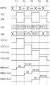
Data is written to the pixel 10 for the first time while image data is supplied to the source lines, and data is written to the pixel for the second time while image data is held by the same source lines. Therefore, the image data may be charged to the source line only once. Further, as described above, by providing two source lines, the operation of the pixels 10 in the nth row and the pixels 10 in the (n + 1) th row can be performed in parallel, and therefore, the writing of image data can be speeded up.
Fig. 2 shows a specific example of the circuit 11 and the pixels 10 in the nth to (n + 2) th rows (m, n are natural numbers equal to or greater than 1) in the mth column.
The circuit 11[ m ] may have a structure including a transistor 107 and a transistor 108. A gate of the transistor 107 is electrically connected to a wiring 124, and a gate of the transistor 108 is electrically connected to a wiring 123. One of a source and a drain of the transistor 107 is electrically connected to the wiring 125[ m ], and one of a source and a drain of the transistor 108 is electrically connected to the wiring 126[ m ]. The other of the source and the drain of the transistor 107 and the other of the source and the drain of the transistor 108 are electrically connected to an output line for the m-th column of the source driver 12.
The wiring 123 and the wiring 124 function as signal lines for controlling conduction of the transistor 108 or the transistor 107. The wiring 125[ m ] and the wiring 126[ m ] are used as source lines.
The wiring 125[ m ] is electrically connected to one electrode of the capacitor 105. The wiring 126[ m ] is electrically connected to one electrode of the capacitor 106. The other electrode of the capacitor 105 and the other electrode of the capacitor 106 are electrically connected to a wiring 135 to which a fixed potential is supplied. Note that as described above, the plurality of capacitors 105 and the plurality of capacitors 106 may be connected in parallel. Further, the capacitor 105 and the capacitor 106 may not be provided.
When the transistor 107 is turned on, the image DATA (DATA) output from the source driver 12 is output to the wiring 126[ m ]. When the transistor 108 is on, image DATA (DATA) output from the source driver is output to the wiring 125[ m ]. Further, by rendering the transistor 107 nonconductive after the above-mentioned image DATA is output, the wiring 126[ m ] is in a floating state and the image DATA (DATA) is held in the wiring 126[ m ]. By putting the transistor 108 in non-conduction, the wiring 125[ 2], [ m ] is in a floating state and the image DATA (DATA) is held at the wiring 125[ 2], [ m ].
Note that the above description of the structure of the circuit 11 is merely an example, and any other structure may be employed as long as it has a function of selectively supplying data to the wiring 125 and the wiring 126 and a function of floating the wiring 125 and the wiring 126.
The pixel 10 includes a transistor 101, a transistor 102, a transistor 103, a capacitor 104, and a circuit block 110. The circuit block 110 may include transistors, capacitors, display elements, and the like, and the details thereof will be described later.
One of a source and a drain of the transistor 101 is electrically connected to one of a source and a drain of the transistor 102. One of a source and a drain of the transistor 102 is electrically connected to one electrode of the capacitor 104. The other electrode of the capacitor 104 is electrically connected to one of a source and a drain of the transistor 103. One of a source and a drain of the transistor 103 is electrically connected to the circuit block 110.
Here, a wiring connecting one of the source and the drain of the transistor 103 and the other electrode of the capacitor 104 to the circuit block is referred to as a node NM. The display elements included in the circuit block 110 operate according to the potential of the node NM. In addition, the node NM may be in a floating state by the components of the circuit block 110 connected to the node NM.
The pixel 10[ n, m ] in the n-th row]In (1), the gate of the transistor 101 and the wiring 121[ n ] +1]And (6) electrically connecting. The gate of the transistor 102 and the gate of the transistor 103 are connected to the wiring 121[ n ]]And (6) electrically connecting. The other of the source and the drain of the transistor 101 and the other of the source and the drain of the transistor 103 are connected to the wiring 125[ m ]]And (6) electrically connecting. The other of the source and the drain of the transistor 102 is capable of supplying a specific potential "V ref "are electrically connected.
Pixel 10[ n +1] m in row n +1]In (1), the gate of the transistor 101 and the wiring 121[ n ] +2]And (6) electrically connecting. The gate of the transistor 102 and the gate of the transistor 103 are connected to the wiring 121[ n ] +1]And (6) electrically connecting. The other of the source and the drain of the transistor 101 and the other of the source and the drain of the transistor 103 are connected to the wiring 126[ m ]]And (6) electrically connecting. The other of the source and the drain of the transistor 102 is capable of supplying a specific potential "V ref "are electrically connected.
The wiring 121 is used as a gate line and is electrically connected to the gate driver 13 (see fig. 1).
As described above, the pixels 10 are alternately connected to different source lines (the wiring 125 or the wiring 126) every other row. In addition, the gate line (wiring 121) is electrically connected to two pixels 10 adjacent in the column direction.
As being able to supply "V ref For example, a power supply line electrically connected to the components of the circuit block 110 may be used as the wiring.
In order to perform the capacitive coupling operation described later, it is necessary to supply the data and "V" supplied for the first time to the pixel 10 in the same period ref ". Thus, when "V" is supplied from the source line ref "time, at least the source line for supplying data and the source line for supplying" V "are required ref Or the source line of the second data.
In one embodiment of the present invention, "V" is supplied from a power supply line or the like ref ", the first data supply or the second data supply can be performed using one signal line by switching the timing. That is, the display device according to one embodiment of the present invention can be configured using a small number of wirings.
The node NM is a storage node, and data supplied to the wiring 125 or the wiring 126 can be written to the node NM by turning on the transistor 103. Further, by making the transistor 103 non-conductive, the data can be held in the node NM. By using a transistor with extremely low off-state current as the transistor 103, the potential of the node NM can be held for a long time. As the transistor, for example, a transistor using a metal oxide for a channel formation region (hereinafter, referred to as an OS transistor) can be used.
The OS transistor can be used not only for the transistor 103 but also for other transistors constituting the pixel 10. Further, an OS transistor may be used as a transistor constituting the circuit 11. In addition, a transistor including Si in a channel formation region (hereinafter, referred to as an Si transistor) may be used for the pixel 10 and the circuit 11. Alternatively, both an OS transistor and an Si transistor may be used. Examples of the Si transistor include a transistor containing amorphous silicon, a transistor containing crystalline silicon (typically, low-temperature polycrystalline silicon or single crystal silicon), and the like.
As a semiconductor material used for the OS transistor, a metal oxide having an energy gap of 2eV or more, preferably 2.5eV or more, and more preferably 3eV or more can be used. An oxide semiconductor containing indium or the like is typical, and for example, CAAC-OS or CAC-OS or the like mentioned later can be used. CAAC-OS is suitable for transistors where atoms constituting a crystal are stable and reliability is important. The CAC-OS exhibits high mobility characteristics and is suitable for a transistor or the like which performs high-speed driving.
The OS transistor has a large energy gap and exhibits an extremely low off-state current characteristic. Unlike the Si transistor, the OS transistor does not cause impact ionization, avalanche breakdown, short channel effect, or the like, and thus can form a highly reliable circuit.
As the semiconductor layer In the OS transistor, for example, a film represented by "In-M-Zn based oxide" containing indium, zinc, and M (a metal such as aluminum, titanium, gallium, germanium, yttrium, zirconium, lanthanum, cerium, tin, neodymium, or hafnium) can be used.
When the oxide semiconductor constituting the semiconductor layer is an In-M-Zn based oxide, the atomic ratio of the metal elements of the sputtering target for forming the In-M-Zn oxide film preferably satisfies in.gtoreq.M and Zn.gtoreq.M. The atomic ratio of the metal elements of such a sputtering target is preferably In M: zn = 1. Note that the atomic ratio of the semiconductor layers to be formed may vary within ± 40% of the atomic ratio of the metal element in the sputtering target.
As the semiconductor layer, an oxide semiconductor having a low carrier density can be used. For example, a semiconductor layer having a carrier density of 1 × 10 can be used 17 /cm 3 Hereinafter, it is preferably 1X 10 15 /cm 3 Hereinafter, more preferably 1 × 10 13 /cm 3 Hereinafter, more preferably 1 × 10 11 /cm 3 Hereinafter, more preferably less than 1X 10 10 /cm 3 ,1×10 -9 /cm 3 The oxide semiconductor described above. Such an oxide semiconductor is referred to as an oxide semiconductor which is intrinsic to high purity or substantially intrinsic to high purity. Since the oxide semiconductor has a low impurity concentration, the oxide semiconductor can be said to have stable characteristics.
Note that the present invention is not limited to the above description, and a material having an appropriate composition may be used in accordance with the semiconductor characteristics and the electrical characteristics (field effect mobility, threshold voltage, and the like) of a transistor which are required. In addition, it is preferable to appropriately set the carrier density, the impurity concentration, the defect density, the atomic ratio of the metal element to oxygen, the interatomic distance, the density, and the like of the semiconductor layer so as to obtain desired semiconductor characteristics of the transistor.
When the oxide semiconductor constituting the semiconductor layer contains silicon or carbon which is one of group 14 elements, oxygen defects increase, and the semiconductor layer becomes n-type. Therefore, the concentration of silicon or carbon in the semiconductor layer (concentration measured by secondary ion mass spectrometry) was set to 2 × 10 18 atoms/cm 3 Hereinafter, it is preferably 2X 10 17 atoms/cm 3 The following.
In addition, when an alkali metal or an alkaline earth metal is bonded to an oxide semiconductor, carriers are generated, and an off-state current of a transistor may be increased. Therefore, the concentration of the alkali metal or alkaline earth metal (concentration measured by secondary ion mass spectrometry) of the semiconductor layer was set to 1 × 10 18 atoms/cm 3 Hereinafter, 2 × 10 is preferable 16 atoms/cm 3 The following.
When the oxide semiconductor constituting the semiconductor layer contains nitrogen, electrons as carriers are generated, and the carrier density increases, so that n-type conversion is facilitated. As a result, a transistor using an oxide semiconductor containing nitrogen easily has normally-on characteristics. Therefore, the nitrogen concentration (concentration measured by secondary ion mass spectrometry) of the semiconductor layer is preferably 5 × 10 18 atoms/cm 3 The following.
The semiconductor layer may have a non-single crystal structure. The non-single crystal structure includes, for example, a CAAC-OS (C-Axis Aligned Crystalline Oxide Semiconductor) having a crystal with a C-Axis orientation, a polycrystalline structure, a microcrystalline structure, or an amorphous structure. In the non-single crystalline structure, the defect state density is highest in the amorphous structure, and is lowest in the CAAC-OS.
The oxide semiconductor film having an amorphous structure has, for example, disordered atomic arrangement and has no crystalline component. Alternatively, the oxide film having an amorphous structure has, for example, a completely amorphous structure and does not have a crystal portion.
The semiconductor layer may be a mixed film of two or more of an amorphous structure region, a microcrystalline structure region, a polycrystalline structure region, a CAAC-OS region, and a single crystal structure region. The hybrid film sometimes has, for example, a single-layer structure or a laminated structure including two or more of the above-described regions.
Next, a structure of CAC (Cloud-Aligned Composite) -OS, which is one embodiment of a non-single crystal semiconductor layer, will be described.
The CAC-OS is, for example, a structure in which elements contained in an oxide semiconductor are unevenly distributed, and the size of a material containing the unevenly distributed elements is 0.5nm or more and 10nm or less, preferably 1nm or more and 2nm or less or a size close thereto. Note that a state in which one or a plurality of metal elements are unevenly distributed in an oxide semiconductor and a region including the metal element is mixed in a size of 0.5nm or more and 10nm or less, preferably 1nm or more and 2nm or less, or an approximate size is also referred to as mosaic (mosaic) or patch (patch) in the following.
The oxide semiconductor preferably contains at least indium. Particularly preferably indium and zinc. In addition, one or more selected from aluminum, gallium, yttrium, copper, vanadium, beryllium, boron, silicon, titanium, iron, nickel, germanium, zirconium, molybdenum, lanthanum, cerium, neodymium, hafnium, tantalum, tungsten, magnesium, and the like may be contained.
For example, CAC-OS among In-Ga-Zn oxides (In CAC-OS, in-Ga-Zn oxide may be particularly referred to as CAC-IGZO) means that the material is divided into indium oxide (hereinafter, referred to as InO) X1 (X1 is a real number greater than 0)) or indium zinc oxide (hereinafter, referred to as In) X2 Zn Y2 O Z2 (X2, Y2, and Z2 are real numbers greater than 0)) and gallium oxide (hereinafter referred to as GaO) X3 (X3 is a real number greater than 0)) or gallium zinc oxide (hereinafter, referred to as Ga X4 Zn Y4 O Z4 (X4, Y4, and Z4 are real numbers greater than 0)), and the like, and the mosaic-like InO X1 Or In X2 Zn Y2 O Z2 A structure uniformly distributed in the film (hereinafter, also referred to as a cloud).
In other words, the CAC-OS is of GaO X3 A region containing as a main component In X2 Zn Y2 O Z2 Or InO X1 Is mainly composed ofA composite oxide semiconductor having a mixture of component regions. In this specification, for example, when the atomic ratio of In to the element M In the first region is larger than the atomic ratio of In to the element M In the second region, the In concentration In the first region is higher than that In the second region.
Note that IGZO is a generic term, and may be a compound containing In, ga, zn, and O. A typical example is InGaO 3 (ZnO) m1 (m 1 is a natural number) or In (1+x0) Ga (1-x0) O 3 (ZnO) m0 A crystalline compound represented by (-1. Ltoreq. X0. Ltoreq.1, m0 being an arbitrary number).
The crystalline compound has a single crystal structure, a polycrystalline structure, or a CAAC structure. The CAAC structure is a crystal structure in which a plurality of IGZO nanocrystals have c-axis orientation and are connected in a non-oriented manner on the a-b plane.
On the other hand, CAC-OS is related to the material composition of an oxide semiconductor. CAC-OS refers to the following composition: in the material composition containing In, ga, zn, and O, some of the nanoparticle-like regions containing Ga as a main component and some of the nanoparticle-like regions containing In as a main component were observed to be irregularly dispersed In a mosaic shape. Therefore, in CAC-OS, the crystal structure is a secondary factor.
The CAC-OS does not contain a laminate structure of two or more films different in composition. For example, a structure composed of two layers of a film containing In as a main component and a film containing Ga as a main component is not included.
Note that GaO is sometimes not observed X3 A region containing as a main component In X2 Zn Y2 O Z2 Or InO X1 Is a well-defined boundary between regions of the principal component.
In the case where the CAC-OS contains one or more selected from aluminum, yttrium, copper, vanadium, beryllium, boron, silicon, titanium, iron, nickel, germanium, zirconium, molybdenum, lanthanum, cerium, neodymium, hafnium, tantalum, tungsten, magnesium, and the like in place of gallium, the CAC-OS means a constitution as follows: some of the nano-particle-like regions containing the metal element as a main component and some of the nano-particle-like regions containing In as a main component were observed to be irregularly dispersed In a mosaic shape.
The CAC-OS can be formed by, for example, sputtering without intentionally heating the substrate. In the case of forming the CAC-OS by the sputtering method, as the film forming gas, one or more selected from an inert gas (typically argon), an oxygen gas, and a nitrogen gas may be used. The lower the flow ratio of the oxygen gas in the total flow of the film forming gas at the time of film formation, the better, for example, the flow ratio of the oxygen gas is set to 0% or more and less than 30%, preferably 0% or more and 10% or less.
The CAC-OS has the following characteristics: when measured by the Out-Of-Plane method, which is one Of the X-ray diffraction (XRD) measurements, using a theta/2 theta scan, no clear peak is observed. That is, it was found from the X-ray diffraction measurement that the orientation in the a-b plane direction and the c-axis direction was not present in the measurement region.
In addition, in the electron diffraction pattern of CAC-OS obtained by irradiating an electron beam (also referred to as a nanobeam) having a beam diameter of 1nm, an annular region having high brightness and a plurality of bright spots in the annular region were observed. From this, it is known that the crystal structure of the CAC-OS has an nc (nano-crystal) structure having no orientation in the plane direction and the cross-sectional direction, from the electron diffraction pattern.
In addition, for example, in CAC-OS of In-Ga-Zn oxide, based on EDX-plane analysis images (EDX-mapping) obtained by Energy Dispersive X-ray spectrometry (EDX: energy Dispersive X-ray spectroscopy), it was confirmed that: with a gas of GaO X3 A region containing as a main component and In X2 Zn Y2 O Z2 Or InO X1 The main component regions are unevenly distributed and mixed.
The CAC-OS has a structure different from that of an IGZO compound in which metal elements are uniformly distributed, and has properties different from those of the IGZO compound. In other words, CAC-OS has a GaO X3 Etc. as main component and In X2 Zn Y2 O Z2 Or InO X1 The regions having the main components are separated from each other, and the regions having the elements as the main components are formed in a mosaic shape.
Therein, theIn is X2 Zn Y2 O Z2 Or InO X1 The conductivity of the region having the main component is higher than that of GaO X3 Etc. as the main component. In other words, when carriers flow In X2 Zn Y2 O Z2 Or InO X1 The region containing the main component exhibits conductivity of the oxide semiconductor. Therefore, when In is used X2 Zn Y2 O Z2 Or InO X1 When the region as a main component is distributed in a cloud shape in the oxide semiconductor, high field-effect mobility (μ) can be achieved.
On the other hand, with GaO X3 The insulating property of the region containing the above-mentioned component is higher than that of In X2 Zn Y2 O Z2 Or InO X1 Is the region of the main component. In other words, when GaO is used X3 When the region containing the element as a main component is distributed in the oxide semiconductor, a leakage current can be suppressed, and a favorable switching operation can be realized.
Therefore, when CAC-OS is used for the semiconductor element, the heat radiation is caused by GaO X3 Insulation property of the like and In X2 Zn Y2 O Z2 Or InO X1 Can realize high on-state current (I) on ) And high field effect mobility (μ).
In addition, the semiconductor element using the CAC-OS has high reliability. Therefore, CAC-OS is suitable for constituent materials of various semiconductor devices.
An example of an operation of adding two image data will be described with reference to the timing chart shown in fig. 3. In the following description, high potential is represented by "H" and low potential is represented by "L". In addition, "D1" represents image data supplied when writing is performed on the pixels of the first row, "D2" represents image data supplied when writing is performed on the pixels of the second row, and "D3" represents image data supplied when writing is performed on the pixels of the third row. As "V ref ", for example, 0V, GND potential, or a specific reference potential may be used.
First, an operation of writing "D1" to the node NM [ n, m ] of the pixel 10[ n, m ] of the n-th row is explained. Note that here, detailed changes due to the structure, operation timing, and the like of the circuit are not considered in the distribution, coupling, or loss of the potential. The potential variation caused by the capacitive coupling depends on the capacity ratio of the supply side to the supplied side, but for the sake of convenience of explanation, it is assumed that the capacitance value of the node NM is sufficiently small.
First, at time T1, the potential of the wiring 123 is set to "H" and the potential of the wiring 124 is set to "L", and the transistor 108 is turned on so that "D1" is supplied to the wiring 125[ m ].
In addition, by making the wiring 121[ n ] at the time T1]Has a potential of "H" in the pixel 10[ n, m ]]The middle transistor 102 is turned on and the potential of one electrode of the capacitor 104 becomes "V ref ". This operation is a reset operation for performing the subsequent addition operation (capacitive coupling operation). In addition, transistor 103 is turned on and node NM [ n, m ]]Written wiring 125[ m ]]The potential of (2). The job is a first write job, the nodes NM [ n, m ]]Becomes "D1".
Then, the wiring 121[ n ]]When the potential of (1) is "L", the transistors 102 and 103 are turned off, and the nodes NM [ n, m ] are turned off]The "D1" is maintained. In addition, capacitor 104 holds "D1-V ref ”。
Here is the writing operation of "D1" in the pixel 10[ n, m ]. The operation of addition of "D1" in pixel [ 10], [ n ], [ m ] and the operation of writing of "D2" in pixel [ 10], [ n +1, m ] are explained below.
By setting the potential of the wiring 123 to "L" and the potential of the wiring 124 to "H" at time T2, the wiring 125[ m ] is in a floating state and is held at "D1". In addition, the transistor 107 is turned on so that "D2" is supplied to the wiring 126[ m ].
In addition, by making wiring 121[ n ] +1 at time T2]Is "H" in the pixel 10[ n, m ]]Middle transistor 101 is turned on to couple node NM [ n, m ] by capacitive coupling of capacitor 104]Is maintained at wiring 125[ 2], [ m ]]Potential "D1" of (a). The job is a second write job, node NM [ n, m ]]To "D1-V ref + D1". At this time, at "V ref =0", node NM [ n, m]Becomes "D1+ D1". That is, data supplied and held in the source line can be attached to the pixel.
In addition, at pixel [ 10], +1, m]The middle transistor 102 is turned on and the potential of one electrode of the capacitor 104 becomes "V ref ". In addition, transistor 103 is turned on and node NM [ n +1, m ]]Is written in the wiring 126[ 2], [ m ]]The potential of (2). The operation is a first write operation, node NM [ n +1, m ]]Becomes "D2".
Here is the writing of "D1+ D1" in the pixel 10[ 2], [ n, m ] work and write work of "D2" in pixel 10[ n +1, m ]. The addition operation of "D2" in pixel [ 10], [ n +1, m ] and the writing operation of "D3" in pixel [ 10], [ n +2, m ] are explained below.
At time T3, the potential of the wiring 123 is set to "H" and the potential of the wiring 124 is set to "L", whereby the wiring 126 is in a floating state and is held at "D2". In addition, the transistor 108 is turned on so that "D3" is supplied to the wiring 125[ m ].
In addition, by making wiring 121[ n ] +2 at time T3]Is "H", in the pixel [ n +1, m ]]Middle transistor 101 is turned on to couple node NM n +1, m by capacitive coupling of capacitor 104]The potential application of (2) is maintained at the wiring 126[ m ], [ m ]]Potential "D2" of (a). This operation is a second write operation, node NM [ n +1, m ]]Becomes "D2-V ref + D2". At this time, at "V ref Node NM [ n +1, m ] when =0 ″]Becomes "D2+ D2".
In addition, at pixel [ 10], +2,m]The middle transistor 102 is turned on and the potential of one electrode of the capacitor 104 becomes "V ref ". In addition, transistor 103 is turned on and node NM [ n +2, m ]]Written in the wiring 125[ 2], [ m ]]The potential of (2). This operation is the first write operation, node NM [ n +2,m]Becomes "D3".
Here, the writing operation of "D2+ D2" in pixel 10[ n ] +1, m ] and the writing operation of "D3" in pixel 10[ n ] +2, m ]. In the pixel [ 10], [ n ], [ 2] m ], by performing the same operation as described above according to the timing chart shown in FIG. 3, "D3+ D3" can be written.
As described above, one embodiment of the present invention can perform the work of adding two pieces of image data at high speed. By adding image data, a potential equal to or higher than the maximum output voltage of the source driver can be supplied to the display element, which contributes to improvement of display luminance, expansion of a dynamic range, and the like. In addition, since the output voltage of the source driver can be about half when performing a standard display, power consumption can be reduced.
In addition, writing to the pixels of the n-th row and the pixels of the n + 1-th row can be performed in parallel, so the frame frequency can be increased. Therefore, the frame frequency can be easily increased even in the case where the horizontal period is short due to an increase in the number of pixels. Further, an embodiment of the present invention is also suitable for a field sequential liquid crystal display device which needs to operate at high speed.
Fig. 4A to 4C are examples of a structure which can be applied to the circuit block 110 and includes an EL element as a display element.
The structure shown in fig. 4A includes a transistor 111, a capacitor 113, and an EL element 114. One of a source and a drain of the transistor 111 is electrically connected to one electrode of the EL element 114. One electrode of the EL element 114 is electrically connected to one electrode of the capacitor 113. The other electrode of the capacitor 113 is electrically connected to the gate of the transistor 111. The gate of the transistor 111 is electrically connected to the node NM.
The other of the source and the drain of the transistor 111 is electrically connected to a wiring 128. The other electrode of the EL element 114 is electrically connected to the wiring 129. The wirings 128 and 129 have a function of supplying power. For example, the wiring 128 may supply a high potential power supply. In addition, the wiring 129 can supply a low potential power source.
Here, the system shown in FIG. 2 is used to supply "V ref The other of the source and the drain of the transistor 102 in this case may be electrically connected to the wiring 128. Because of "V ref "is preferably 0V, GND, or a low potential, so the wiring 128 also has a function of supplying at least any one of these potentials. For the wiring 128, "V" is supplied at the timing of writing data to the node NM ref "and a high potential power source may be supplied at a timing of causing the EL element 114 to emit light. In addition, the other of the source and the drain of the transistor 102 may be connected to the supply of "V ref "are electrically connected to each other.
In the structure shown in fig. 4A, a current flows through the EL element 114 when the potential of the node NM becomes equal to or higher than the threshold voltage of the transistor 111. Therefore, the EL element 114 sometimes starts emitting light at the first writing stage shown in the timing chart of fig. 3, and thus the use of this structure may be limited.
Fig. 4B is a structure in which a transistor 112 is added to the structure of fig. 4A. One of a source and a drain of the transistor 112 is electrically connected to one of a source and a drain of the transistor 111. The other of the source and the drain of the transistor 112 is electrically connected to the EL element 114. A gate of the transistor 112 is electrically connected to a wiring 127. The wiring 127 can be used as a signal line for controlling conduction of the transistor 112.
In this structure, when the potential of the node NM is equal to or higher than the threshold voltage of the transistor 111 and the transistor 112 is on, a current flows through the EL element 114. Therefore, the EL element 114 can be caused to start light emission after the second writing shown in the timing chart of fig. 3.
Fig. 4C is a structure in which a transistor 115 is added to the structure of fig. 4B. One of a source and a drain of the transistor 115 is electrically connected to one of a source and a drain of the transistor 111. The other of the source and the drain of the transistor 115 is electrically connected to a wiring 130. A gate of the transistor 115 is electrically connected to the wiring 131. The wiring 131 can be used as a signal line for controlling conduction of the transistor 115.
The wiring 130 can be electrically connected to a supply source of a specific potential such as a reference potential. Writing of image data can also be stabilized by supplying a specific potential from the wiring 130 to one of the source and the drain of the transistor 111.
Further, the wiring 130 may be connected to the circuit 120 and may be used as a monitor line. The circuit 120 may have at least one of a function of supplying the specific potential, a function of acquiring electrical characteristics of the transistor 111, and a function of generating correction data.
Fig. 5A to 5C are examples of structures which can be applied to the circuit block 110 and include a liquid crystal element as a display element.
The structure shown in fig. 5A includes a capacitor 116 and a liquid crystal element 117. One electrode of the liquid crystal element 117 is electrically connected to one electrode of the capacitor 116. One electrode of the capacitor 116 is electrically connected to the node NM.
The other electrode of the capacitor 116 is electrically connected to the wiring 132. The other electrode of the liquid crystal element 117 is electrically connected to the wiring 133. The wirings 132 and 133 have a function of supplying power. For example, the wirings 132 and 133 may supply a reference potential such as GND or 0V or an arbitrary potential.
Here, the system shown in FIG. 2 is used to supply "V ref The other of the source and the drain of the transistor 102 "can be electrically connected to the wiring 132. In addition, the other of the source and the drain of the transistor 102 may be connected to the supply of "V ref "are electrically connected to each other.
In this configuration, the operation of the liquid crystal element 117 is started when the potential of the node NM becomes equal to or higher than the operation threshold of the liquid crystal element 117. Therefore, the display operation is sometimes started at the stage of the first writing shown in the timing chart of fig. 3, and thus the use of this structure may be limited. However, in the case of the transmissive liquid crystal display device, by performing the operation of turning off the backlight and the like in parallel until the second writing shown in the timing chart of fig. 3, it is possible to suppress the visibility even when an unnecessary display operation occurs.
Fig. 5B is a structure in which a transistor 118 is added to the structure of fig. 5A. One of a source and a drain of the transistor 118 is electrically connected to one electrode of the capacitor 116. The other of the source and the drain of the transistor 118 is electrically connected to the node NM. A gate of the transistor 118 is electrically connected to a wiring 127. The wiring 127 can be used as a signal line for controlling conduction of the transistor 118.
In this structure, the potential of the node NM is applied to the liquid crystal element 117 while the transistor 118 is turned on. Therefore, the operation of the liquid crystal element can be started after the second writing shown in the timing chart of fig. 3.
Further, since the potential supplied to the capacitor 116 and the liquid crystal element 117 is continuously held in a state where the transistor 118 is turned off, it is preferable to reset the potential supplied to the capacitor 116 and the liquid crystal element 117 before rewriting image data. This reset can be performed by, for example, supplying a reset potential to a source line (the wiring 125 or the wiring 126) connected to a pixel and turning on the transistor 102 and the transistor 118 at the same time.
Fig. 5C is a structure in which a transistor 119 is added to the structure of fig. 5B. One of a source and a drain of the transistor 119 is electrically connected to one electrode of the liquid crystal element 117. The other of the source and the drain of the transistor 119 is electrically connected to a wiring 130. A gate of the transistor 119 is electrically connected to the wiring 131. The wiring 131 can be used as a signal line for controlling conduction of the transistor 119.
The circuit 120 electrically connected to the wiring 130 may have a function of resetting the potentials of the supply capacitor 116 and the liquid crystal element 117, similarly to the above description of fig. 4C.
Furthermore, although fig. 4 and 5 show that "V" is supplied from the power supply line ref "but" V "may be supplied from a gate line ref ". For example, as shown in FIG. 6A, in the pixel [ 10], [ n]May also be supplied with "V" from the wiring 121 ref ". As shown in fig. 3, since when "D1" is written (when the transistor 103 is turned on), wiring 121[ 2], +1]Is supplied with a potential corresponding to "L", so that the potential can be used as "V" ref ”。
As shown in fig. 6B and 6C, the transistors 101, 102, and 103 may have a structure in which a back gate is provided. Fig. 6B shows a structure in which a back gate is electrically connected to a front gate, which has the effect of increasing on-state current. Fig. 6C shows a structure in which a back gate is electrically connected to a wiring 134 capable of supplying a constant potential, which can control the threshold voltage of a transistor. In addition, the back gate may be provided in the transistors included in the circuit block 110 illustrated in fig. 4A to 4C and fig. 5A to 5C.
The configuration shown in fig. 7 may be employed as a display device including pixels that hold data in the source lines and use the data for addition operation.
In the display device shown in fig. 7, the basic structure of the pixels is the same as that of the display device shown in fig. 2, and is different from the display device shown in fig. 2 in that one source line is provided for each column and two gate lines are provided for each row. In addition, a circuit 14 is provided instead of the circuit 11.
The wiring 121 and the wiring 122 are provided as gate lines. A wiring 121 is electrically connected to a gate of the transistor 102 and a gate of the transistor 103. The wiring 122 is electrically connected to the gate of the transistor 101.
The structure shown in fig. 7 also performs the first writing when the source line is supplied with image data and performs the second writing when the source line holds image data. Note that all pixels in the column direction are connected to one source line, so the writing speed cannot be increased by parallel operation. On the other hand, when the source line holds image data, power gating is performed in an output circuit in the source driver, and power consumption due to leakage current or the like can be reduced.
An example of the operation of adding two image data and the power gating of the source driver will be described with reference to the timing chart shown in fig. 8.
First, an operation of writing the image data "D1" to the node NM [ n, m ] of the pixel 10[ n, n ] of the n-th row is explained. Note that here, detailed changes due to the structure, operation timing, and the like of the circuit are not considered in the distribution, coupling, or loss of the potential.
At time T1, the potential of the wiring 123 is set to "H" and the transistor 109 is turned on so that "D1" is supplied to the wiring 125[ m ].
In addition, at time T1, the wiring 121[ n ]]Is "H", in the pixel 10[ n, m ]]The middle transistor 103 is turned on and the potential of one electrode of the capacitor 104 becomes "V ref ". This operation is a reset operation for performing the subsequent addition operation (capacitive coupling operation). In addition, transistor 102 is turned on and node NM [ n, m ] is turned on]Written in the wiring 125[ 2], [ m ]]The potential of (2). The operation is a first write operation, node NM [ n, m ]]Becomes "D1".
Then, by making the wiring 121 2 at the time T2]The potential of (3) is "L", the potential of the wiring 123 is "L", the transistor 102 and the transistor 103 are turned off, and the node NM [ n, m ] is set to be non-conductive]Retention of "D1". In addition, capacitor 104 holds "D1-V ref ". Further, wiring 125[ 2], [ m ]]Is in a floating state and remains "D1".
Here is the writing operation of "D1" in the pixel 10[ n, m ]. Next, the operation of addition of "D1" in the pixel [ 10], [ n, m ] is explained.
By making the wiring 122[ n ] at the time T2]Is "H" in the pixel 10[ n, m ]]The middle transistor 101 is turned on to couple the node NM [ n, m ] by the capacitive coupling of the capacitor 104]Is applied to the wiring 125[ m ]]Potential "D1" of (a). The job is a second write job, node NM [ n, m ]]Becomes "D1-V ref + D1". At this time, at "V ref Node NM [ n, m ] when =0 ″]Becomes "D1+ D1". That is, data supplied and held in the source line can be attached to the pixel.
After the time T3, the same operation as described above is repeated to write the image DATA (DATA) to the pixels 10 in the next row or later.
Since the source line holds data during the period from time T2 to time T3, the output operation of the source driver 12 is not necessary. Therefore, the operation of the output circuit of the source driver 12 can be stopped during this period. This period is at most about half of the period for writing the image data to the pixels 10, and therefore, power consumption can be significantly reduced.
Next, a simulation result in which the configuration of the circuit block shown in fig. 5A (see fig. 9) is employed for the pixel 10 of the display device shown in fig. 2 will be described. The parameters are as follows. The transistor size is set to L/W =4 μm/200 μm (the transistor included in the circuit 11), L/W =4 μm/4 μm (the transistor included in the pixel 10), the source line resistance value is set to 1k Ω (corresponding to the resistance value between the circuit 11 and each pixel), the capacitance value of the capacitor Csl is set to 100pF (corresponding to 1000 capacitors of 100fF connected to the source line), the capacitance value of the capacitor C1 is set to 500fF, the capacitance value of the capacitor Cs is set to 100fF, the capacitance value of the liquid crystal element Clc is set to 40fF, the maximum image DATA (DATA) is 5V, and "V" is set to V ref "set to 0V, and common electrodes CsCOM and TCOM set to 0V. In addition, "H" is set to +20V and "L" is set to-20V. In addition, SPICE was used as circuit simulation software.
Fig. 11 shows a simulation result when the circuit shown in fig. 9 is operated according to the timing chart shown in fig. 10. SMP1 and SMP2 are gate lines for controlling the operation of the circuit 11. SL1 is the source line connected to pixel 10[ n ], and SL2 is the source line connected to pixel 10[ n +1 ]. GL [ n ] is a gate line connected to pixel 10[ n ], GL [ n +2] is a gate line connected to pixel 10[ n ] +1, and GL [ n +1] is a gate line connected to pixel 10[ n ] and pixel 10[ n ] +1. D1 corresponds to the image DATA (DATA) supplied to pixel 10[ n ], D2 corresponds to the image DATA (DATA) supplied to pixel 10[ n +1], and D3 corresponds to the image DATA (DATA) supplied to pixel 10[ n +2] (not shown).
Fig. 11 is a simulation result of voltages in the node NM [ n ] and the node NM [ n +1] when +5V is input as the image DATA (DATA). Confirming that: at the node NM [ n ], the first writing is performed at the timing when GL [ n ] is "H" and the second writing is performed at the timing when GL [ n +1] is "H", and image DATA (DATA) is added. The same applies to node NM [ n +1 ].
Fig. 12 is a simulation result of voltages in the node NM [ n ] and the node NM [ n +1] when-5V to +5V are input as the image DATA (DATA). It was confirmed that the image DATA (DATA) was added in any of the above cases.
From the above simulation results, it was confirmed that the potential held by the capacitor to the source line was added to the pixel as a data voltage. In the display device according to one embodiment of the present invention, since the writing period from the source driver to the pixel in one horizontal period can be substantially once, the display device is preferably applied to a display device which requires high-speed operation.
This embodiment can be implemented in combination with the structures described in other embodiments and the like as appropriate.
(embodiment mode 2)
In this embodiment, a configuration example of a display device using a liquid crystal element and a configuration example of a display device using an EL element are described. Note that in this embodiment, the constituent elements, operations, and functions of the display device described in embodiment 1 are omitted.
Fig. 13A to 13C are diagrams illustrating a structure of a display device to which one embodiment of the present invention can be applied.
In fig. 13A, a sealant 4005 is provided so as to surround a display portion 215 provided over a first substrate 4001, and the display portion 215 is sealed by the sealant 4005 and a second substrate 4006.
The pixel 10 described in embodiment 1 and the like can be provided in the display portion 215. Note that a scanning line driver circuit described below corresponds to a gate driver, and a signal line driver circuit corresponds to a source driver.
In fig. 13A, the scanning line driver circuit 221a, the signal line driver circuit 231a, the signal line driver circuit 232a, and the common line driver circuit 241a each include a plurality of integrated circuits 4042 provided over a printed circuit board 4041. The integrated circuit 4042 is formed of a single crystal semiconductor or a polycrystalline semiconductor. The common line driver circuit 241a has a function of supplying a predetermined potential to the wirings 128, 129, 132, 133, 135 and the like described in embodiment 1.
Various signals and potentials are supplied to the scanning line driver circuit 221a, the common line driver circuit 241a, the signal line driver circuit 231a, and the signal line driver circuit 232a through an FPC (Flexible printed circuit) 4018.
The integrated circuit 4042 included in the scan line driver circuit 221a and the common line driver circuit 241a has a function of supplying a selection signal to the display portion 215. The integrated circuit 4042 included in the signal line driver circuit 231a and the signal line driver circuit 232a has a function of supplying image data to the display portion 215. The integrated circuit 4042 is mounted in a region different from a region surrounded by the sealant 4005 over the first substrate 4001.
Note that a connection method of the integrated circuit 4042 is not particularly limited, and a wire bonding method, a COG (Chip On Glass) method, a TCP (Tape Carrier Package) method, a COF (Chip On Film) method, or the like can be used.
Fig. 13B shows an example in which an integrated circuit 4042 included in the signal line driver circuit 231a and the signal line driver circuit 232a is mounted by the COG method. In addition, a system-on-panel (system-on-panel) can be formed by forming a part or the whole of the driver circuit over a substrate over which the display portion 215 is formed.
Fig. 13B shows an example in which the scanning line driver circuit 221a and the common line driver circuit 241a are formed over a substrate over which the display portion 215 is formed. By forming the driver circuit and the pixel circuit in the display portion 215 at the same time, the number of components can be reduced. Thereby, productivity can be improved.
In fig. 13B, a sealant 4005 is provided so as to surround the display portion 215, the scan line driver circuit 221a, and the common line driver circuit 241a provided over the first substrate 4001. The second substrate 4006 is provided over the display portion 215, the scan line driver circuit 221a, and the common line driver circuit 241 a. Thus, the display portion 215, the scan line driver circuit 221a, and the common line driver circuit 241a are sealed together with the display element by the first substrate 4001, the sealant 4005, and the second substrate 4006.
Although fig. 13B shows an example in which the signal line driver circuit 231a and the signal line driver circuit 232a are separately formed and mounted on the first substrate 4001, one embodiment of the present invention is not limited to this structure. In addition, a scan line driver circuit or a common line driver circuit may be separately formed and mounted. Alternatively, a part of the signal line driver circuit, a part of the scanning line driver circuit, or a part of the common line driver circuit may be separately formed and mounted. As shown in fig. 13C, the signal line driver circuit 231a and the signal line driver circuit 232a may be formed over a substrate over which the display portion 215 is formed.
Further, the display device may include a panel in which a display element is in a sealed state, and a module in which an IC or the like including a controller is mounted on the panel.
The display portion and the scan line driver circuit which are provided over the first substrate include a plurality of transistors. As the transistor, the transistor described in the above embodiment mode can be used.
The transistors included in the peripheral driver circuit and the transistors included in the pixel circuit of the display portion may have the same or different structures. The transistors included in the peripheral driver circuit may all have the same structure, or two or more structures may be combined. Similarly, the transistors included in the pixel circuit may have the same structure, or two or more structures may be combined.
In addition, an input device may be provided over the second substrate 4006. The structure of providing the input device 4200 to the display device shown in fig. 13A to 13C can be used as a touch panel.
The sense element (also referred to as a sensor element) included in the touch panel according to one embodiment of the present invention is not particularly limited. Various sensors capable of detecting the approach or contact of a detection object such as a finger or a stylus pen can also be used as the sensing element.
For example, various sensor systems such as a capacitance type, a resistance film type, a surface acoustic wave type, an infrared type, an optical type, and a pressure sensitive type can be used.
In this embodiment, a touch panel including a capacitance-type sensor element will be described as an example.
The capacitance type includes a surface type capacitance type, a projection type capacitance type, and the like. The projection type capacitance includes a self capacitance and a mutual capacitance. The use of mutual capacitance is preferred because multipoint sensing can be done simultaneously.
The touch panel according to one embodiment of the present invention can have various structures such as a structure in which a display device and a sensor element which are manufactured separately are bonded to each other, and a structure in which an electrode or the like constituting the sensor element is provided over one or both of a substrate supporting the display element and a counter substrate.
Fig. 14A and 14B illustrate an example of a touch panel. Fig. 14A is a perspective view of the touch panel 4210. Fig. 14B is a perspective view of the input device 4200. Note that only typical constituent elements are shown for clarity.
The touch panel 4210 has a structure in which a display device and a sensing element which are separately manufactured are attached to each other.
The touch panel 4210 includes an input device 4200 and a display device which are provided to overlap.
The input device 4200 includes a substrate 4263, an electrode 4227, an electrode 4228, a plurality of wirings 4237, a plurality of wirings 4238, and a plurality of wirings 4239. For example, the electrode 4227 may be electrically connected to the wiring 4237 or the wiring 4239. In addition, the electrode 4228 may be electrically connected to a wiring 4239. The FPC4272b can be electrically connected to each of the plurality of wirings 4237, the plurality of wirings 4238, and the plurality of wirings 4239. The FPC4272b may be provided with an IC4273b.
A touch sensor may be provided between the first substrate 4001 and the second substrate 4006 of the display device. When a touch sensor is provided between the first substrate 4001 and the second substrate 4006, an optical touch sensor using a photoelectric conversion element can be used in addition to an electrostatic capacitance type touch sensor.
Fig. 15A and 15B are sectional views taken along the chain line N1-N2 in fig. 13B. The display device shown in fig. 15A and 15B includes an electrode 4015, and the electrode 4015 and a terminal included in an FPC4018 are electrically connected to each other through an anisotropic conductive layer 4019. In fig. 15A and 15B, an electrode 4015 is electrically connected to a wiring 4014 in an opening formed in an insulating layer 4112, an insulating layer 4111, and an insulating layer 4110.
The electrode 4015 and the first electrode layer 4030 are formed using the same conductive layer, and the wiring 4014 and source and drain electrodes of the transistor 4010 and the transistor 4011 are formed using the same conductive layer.
In addition, the display portion 215 and the scan line driver circuit 221a provided over the first substrate 4001 include a plurality of transistors. Fig. 15A and 15B show a transistor 4010 included in the display portion 215 and a transistor 4011 in the scan line driver circuit 221 a. Although bottom-gate transistors are illustrated as the transistors 4010 and 4011 in fig. 15A and 15B, top-gate transistors may be used.
In fig. 15A and 15B, an insulating layer 4112 is provided over the transistor 4010 and the transistor 4011. In addition, in fig. 15B, a partition 4510 is formed over the insulating layer 4112.
In addition, a transistor 4010 and a transistor 4011 are provided over the insulating layer 4102. In addition, the transistor 4010 and the transistor 4011 include an electrode 4017 formed over an insulating layer 4111. The electrode 4017 can be used as a back gate electrode.
In addition, the display device shown in fig. 15A and 15B includes a capacitor 4020. The capacitor 4020 includes an electrode 4021 formed in the same step as the gate electrode of the transistor 4010 and electrodes formed in the same step as the source and drain electrodes. The electrodes overlap each other with an insulating layer 4103 interposed therebetween.
In general, the capacitance of a capacitor provided in a pixel portion of a display device is set so as to be able to hold electric charge for a specified period in consideration of the leakage current of a transistor arranged in the pixel portion, and the like. The capacity of the capacitor may be set in consideration of the off-state current of the transistor.
The transistor 4010 provided in the display portion 215 is electrically connected to a display element. Fig. 15A shows an example of a liquid crystal display device in which a liquid crystal element is used as a display element. In fig. 15A, a liquid crystal element 4013 which is a display element includes a first electrode layer 4030, a second electrode layer 4031, and a liquid crystal layer 4008. Note that the insulating layers 4032 and 4033 which function as alignment films are provided so as to sandwich the liquid crystal layer 4008. The second electrode layer 4031 is provided on the second substrate 4006 side, and the first electrode layer 4030 and the second electrode layer 4031 overlap with each other with the liquid crystal layer 4008 interposed therebetween.
The spacer 4035 is a columnar spacer obtained by selectively etching an insulating layer, and is provided for controlling a space (cell gap) between the first electrode layer 4030 and the second electrode layer 4031. Note that a spherical spacer may also be used.
Further, as necessary, an optical member (optical substrate) such as a black matrix (light-shielding layer), a colored layer (color filter), a polarizing member, a phase difference member, and an antireflection member may be appropriately provided. For example, circular polarization using a polarizing substrate and a phase difference substrate may be used. Further, as the light source, a backlight, a side light, or the like may be used. As the backlight or side light, micro-LEDs and the like may be used.
In the display device shown in fig. 15A, a light-shielding layer 4132, a colored layer 4131, and an insulating layer 4133 are provided between the second substrate 4006 and the second electrode layer 4031.
Examples of materials that can be used for the light-shielding layer include carbon black, titanium black, metals, metal oxides, and composite oxides containing a solid solution of a plurality of metal oxides. The light-shielding layer may be a film containing a resin material or a thin film containing an inorganic material such as a metal. Further, a laminated film of films including materials of the colored layers may be used for the light-shielding layer. For example, a stacked structure of a film including a material of a colored layer for transmitting light of a certain color and a film including a material of a colored layer for transmitting light of another color may be employed. It is preferable that the colored layer and the light-shielding layer are made of the same material because the process can be simplified, in addition to the use of the same equipment.
Examples of materials that can be used for the colored layer include metal materials, resin materials, and resin materials containing pigments or dyes. The light-shielding layer and the colored layer can be formed by, for example, an inkjet method.
In addition, the display device shown in fig. 15A and 15B includes an insulating layer 4111 and an insulating layer 4104. As the insulating layer 4111 and the insulating layer 4104, insulating layers which are less likely to transmit impurity elements are used. By sandwiching the semiconductor layer of the transistor between the insulating layer 4111 and the insulating layer 4104, impurities from the outside can be prevented from being mixed.
In addition, a light-emitting element (EL element) using electroluminescence can be used as a display element included in a display device. An EL element has a layer containing a light-emitting compound (also referred to as an EL layer) between a pair of electrodes. When a potential difference higher than the threshold voltage of the EL element is generated between the pair of electrodes, holes are injected into the EL layer from the anode side, and electrons are injected into the EL layer from the cathode side. The injected electrons and holes are recombined in the EL layer, whereby the light-emitting compound contained in the EL layer emits light.
The EL element is distinguished depending on whether the light emitting material is an organic compound or an inorganic compound, and generally the former is referred to as an organic EL element, and the latter is referred to as an inorganic EL element.
In an organic EL element, when a voltage is applied, electrons are injected from one electrode into an EL layer, and holes are injected from the other electrode into the EL layer. By recombination of these carriers (electrons and holes), the light-emitting organic compound forms an excited state, and light is emitted when the light-emitting organic compound returns from the excited state to a ground state. Due to such a mechanism, such a light-emitting element is called a current excitation type light-emitting element.
The EL layer may contain, in addition to the light-emitting compound, a substance having a high hole-injecting property, a substance having a high hole-transporting property, a hole-blocking material, a substance having a high electron-transporting property, a substance having a high electron-injecting property, a bipolar substance (a substance having a high electron-transporting property and a high hole-transporting property), or the like.
The EL layer can be formed by a method such as a vapor deposition method (including a vacuum vapor deposition method), a transfer method, a printing method, an ink-jet method, or a coating method.
Inorganic EL elements are classified into dispersion-type inorganic EL elements and thin-film-type inorganic EL elements according to their element structures. The dispersion-type inorganic EL element includes a light-emitting layer in which particles of a light-emitting material are dispersed in a binder, and its light emission mechanism is donor-acceptor recombination type light emission utilizing a donor level and an acceptor level. The thin film type inorganic EL element is a structure in which a light emitting layer is sandwiched between dielectric layers, and the dielectric layers sandwiching the light emitting layer are sandwiched between electrodes, and its light emission mechanism is a localized type light emission utilizing inner shell electron transition of metal ions. Note that here, an organic EL element is used as a light-emitting element.
At least one of the pair of electrodes of the light-emitting element is made transparent in order to extract light emission. A transistor and a light-emitting element are formed over a substrate. The light emitting element has a top emission structure light emitting element which takes out light emission from a surface on the opposite side of the substrate, a bottom emission structure light emitting element which takes out light emission from a surface on the substrate side, and a double-sided emission structure light emitting element which takes out light emission from both surfaces. The light-emitting element may have any of the above structures.
Fig. 15B shows an example of a light-emitting display device (also referred to as an "EL display device") using a light-emitting element as a display element. A light-emitting element 4513 which is used as a display element is electrically connected to a transistor 4010 provided in the display portion 215. Although the light-emitting element 4513 has a stacked-layer structure of the first electrode layer 4030, the light-emitting layer 4511, and the second electrode layer 4031, the structure is not limited to this. The structure of the light-emitting element 4513 can be changed as appropriate depending on the direction in which light is extracted from the light-emitting element 4513, and the like.
The partition wall 4510 is formed using an organic insulating material or an inorganic insulating material. In particular, it is preferable to form an opening in the first electrode layer 4030 using a photosensitive resin material, and to form a side surface of the opening as an inclined surface having a continuous curvature.
The light-emitting layer 4511 may be formed using one layer or a stack of a plurality of layers.
The light-emitting color of the light-emitting element 4513 may be white, red, green, blue, cyan, magenta, yellow, or the like depending on the material constituting the light-emitting layer 4511.
As a method for realizing color display, there are the following methods: a method of combining the light-emitting element 4513 whose emission color is white and a colored layer; and a method in which a light-emitting element 4513 which emits light of a different color is provided for each pixel. The former method has higher productivity than the latter method. On the other hand, in the latter method, the light-emitting layer 4511 needs to be formed for each pixel, so that the productivity is lower than that in the former method. However, in the latter method, a higher emission color can be obtained than in the former method. In the latter method, the light-emitting element 4513 has a microcavity structure, whereby color purity can be further improved.
The light-emitting layer 4511 may contain an inorganic compound such as a quantum dot. For example, quantum dots can be used as a light-emitting material by using the quantum dots for a light-emitting layer.
In order to prevent oxygen, hydrogen, moisture, carbon dioxide, or the like from entering the light-emitting element 4513, a protective layer may be formed over the second electrode layer 4031 and the partition 4510. As the protective layer, silicon nitride oxide, aluminum nitride, aluminum oxynitride, aluminum nitride oxide, DLC (Diamond-Like Carbon), or the Like can be formed. Further, a filler 4514 is provided in a space sealed by the first substrate 4001, the second substrate 4006, and the sealant 4005, and is sealed. In this way, it is preferable to seal (encapsulate) the substrate using a protective film (adhesive film, ultraviolet curable resin film, or the like) or a covering material, which has high airtightness and causes little outgassing, so as not to be exposed to outside air.
As the filler 4514, in addition to an inert gas such as nitrogen or argon, an ultraviolet-curable resin or a thermosetting resin may be used, and for example, PVC (polyvinyl chloride), an acrylic resin, polyimide, an epoxy resin, a silicone resin, PVB (polyvinyl butyral), EVA (ethylene vinyl acetate), or the like may be used. The filler 4514 may also contain a desiccant.
As the sealant 4005, a glass material such as glass frit, or a resin material such as a curable resin, a photocurable resin, or a thermosetting resin that is curable at room temperature such as a two-liquid mixture resin can be used. The sealant 4005 may also contain a desiccant.
Further, as necessary, an optical film such as a polarizing plate, a circularly polarizing plate (including an elliptically polarizing plate), a retardation plate (λ/4 plate, λ/2 plate), a color filter, or the like may be appropriately provided on the light emitting surface of the light emitting element. Further, an antireflection film may be provided on the polarizing plate or the circular polarizing plate. For example, anti-glare treatment for reducing reflection glare by diffusing reflected light using surface irregularities may be performed.
By providing the light-emitting element with a microcavity structure, light with high color purity can be extracted. In addition, by combining the microcavity structure and the color filter, reflection glare can be prevented, and visibility of an image can be improved.
The first electrode layer and the second electrode layer (also referred to as a pixel electrode layer, a common electrode layer, a counter electrode layer, or the like) which apply a voltage to the display element may have light transmittance or reflectance selected depending on the direction of light extraction, the place where the electrode layer is provided, and the pattern structure of the electrode layer.
The first electrode layer 4030 and the second electrode layer 4031 can be formed using a light-transmitting conductive material such as indium oxide containing tungsten oxide, indium zinc oxide containing tungsten oxide, indium oxide containing titanium oxide, indium tin oxide containing titanium oxide, indium zinc oxide, or indium tin oxide to which silicon oxide is added.
The first electrode layer 4030 and the second electrode layer 4031 can be formed using one or more metals such as tungsten (W), molybdenum (Mo), zirconium (Zr), hafnium (Hf), vanadium (V), niobium (Nb), tantalum (Ta), chromium (Cr), cobalt (Co), nickel (Ni), titanium (Ti), platinum (Pt), aluminum (Al), copper (Cu), and silver (Ag), or an alloy thereof or a metal nitride thereof.
In addition, the first electrode layer 4030 and the second electrode layer 4031 can be formed using a conductive composition containing a conductive polymer (also referred to as a conductive polymer). As the conductive polymer, a so-called pi electron conjugated conductive polymer can be used. For example, polyaniline or a derivative thereof, polypyrrole or a derivative thereof, polythiophene or a derivative thereof, or a copolymer or a derivative thereof composed of two or more kinds of aniline, pyrrole, and thiophene can be given.
Further, since a transistor is easily broken by static electricity or the like, a protection circuit for protecting a driver circuit is preferably provided. The protection circuit is preferably formed using a nonlinear element.
Note that as shown in fig. 16, a stacked structure in which the transistor and the capacitor include an overlapping region in the height direction may be employed. For example, by disposing the transistor 4011 and the transistor 4022 which constitute the driver circuit so as to overlap with each other, a display device with a narrow frame can be realized. Further, by disposing the transistor 4010, the transistor 4023, the capacitor 4020, and the like which constitute the pixel circuit so as to partially include an overlapping region, the aperture ratio and the resolution can be improved. Fig. 16 shows an example in which the stacked structure is applied to the liquid crystal display device shown in fig. 15A, but the stacked structure may be applied to the EL display device shown in fig. 15B.
In addition, in the pixel circuit, a light-transmitting conductive film having high light transmittance to visible light is used as an electrode and a wiring, and the light transmittance in the pixel can be increased, so that the aperture ratio can be substantially increased. Further, since the semiconductor layer has light-transmitting properties even when an OS transistor is used, the aperture ratio can be further increased. This is also effective when a transistor or the like does not have a stacked structure.
Further, a display device may be configured by combining a liquid crystal display device and a light-emitting device.
The light emitting device is disposed on the opposite side of the display surface or at an end portion of the display surface. The light-emitting device has a function of supplying light to the display element. The light emitting device is called a backlight.
Here, the light-emitting device may include a plate-shaped or film-shaped light guide portion (also referred to as a light guide plate) and a plurality of light-emitting elements that emit light of different colors. By disposing the light emitting element near the side surface of the light guide portion, light can be emitted from the side surface of the light guide portion to the inside. The light guide portion includes a mechanism (also referred to as a light extraction mechanism) that changes an optical path, whereby the light emitting device can uniformly irradiate light to the pixel portion of the display panel. Alternatively, a light-emitting device may be disposed directly below a pixel without providing a light guide portion.
The light-emitting device preferably includes light-emitting elements of three colors of red (R), green (G), and blue (B). Further, a white (W) light-emitting element may be included. Light Emitting Diodes (LED) are preferably used as these Light Emitting elements.
The light-emitting element preferably has an extremely high color purity, and has an emission spectrum with a Full Width at Half Maximum (FWHM) of 50nm or less, preferably 40nm or less, more preferably 30nm or less, and still more preferably 20nm or less. Note that the smaller the full width at half maximum of the emission spectrum, the better, and for example, 1nm or more may be used. Thus, when color display is performed, vivid display with high color reproducibility can be performed.
In addition, it is preferable to use a red light-emitting element having an emission spectrum with a peak wavelength in a range of 625nm to 650 nm. In addition, it is preferable to use a green light-emitting element having an emission spectrum with a peak wavelength in a range of 515nm to 540 nm. The blue light-emitting element preferably has an emission spectrum with a peak wavelength in a range of 445nm to 470 nm.
The display device sequentially blinks the light-emitting elements of the three colors and simultaneously drives the pixels in synchronization with the blinking of the light-emitting elements, thereby performing color display by a sequential additive color mixing method. This driving method may also be referred to as field sequential driving.
The field sequential driving can display vivid color images. In addition, a smooth moving image can be displayed. Further, by using the above driving method, it is not necessary to configure one pixel by a plurality of sub-pixels of different colors, so that the effective reflection area (also referred to as effective display area or aperture ratio) of one pixel can be enlarged, and bright display can be performed. Further, since it is not necessary to provide a color filter in the pixel, the transmittance of the pixel can be increased, and brighter display can be performed. In addition, the manufacturing process can be simplified, whereby the manufacturing cost can be reduced.
Fig. 17A and 17B are schematic cross-sectional views of a display device capable of field sequential driving. A backlight unit capable of emitting light of each color of RGB is provided on the substrate 4001 side of the display device. Note that in the field sequential driving, since the display colors are emitted in time division of each color of RGB, a color filter is not required.
The backlight unit 4340a shown in fig. 17A has a structure in which a plurality of light-emitting elements 4342 are provided directly below a pixel with a diffuser plate 4352 interposed therebetween. The diffuser plate 4352 has a function of diffusing light emitted from the light-emitting element 4342 to the substrate 4001 side to make luminance uniform in the display portion surface. A polarizing plate may be provided between the light-emitting element 4342 and the diffusion plate 4352 as necessary. The diffusion plate 4352 may not be provided if it is not necessary. The light-shielding layer 4132 may be omitted.
Since the backlight unit 4340a can be disposed directly below the display portion, a large number of light-emitting elements 4342 can be mounted, and bright display can be achieved. Further, there is an advantage that a light guide plate is not necessary and the light efficiency of the light-emitting element 4342 is not easily lost. Note that a lens 4344 for light diffusion may be provided in the light-emitting element 4342 as needed.
A backlight unit 4340B shown in fig. 17B has a structure in which a light guide plate 4341 is provided directly below a pixel with a diffusion plate 4352 interposed therebetween. A plurality of light emitting elements 4342 are provided at an end of the light guide plate 4341. The light guide plate 4341 has a concave-convex shape on the side opposite to the diffusion plate 4352, and thus guided light can be scattered by the concave-convex shape and emitted in the direction of the diffusion plate 4352.
The light-emitting element 4342 may be fixed to the printed circuit board 4347. Note that in fig. 17B, light-emitting elements 4342 of RGB colors are shown to overlap each other, and the light-emitting elements 4342 of RGB colors may be arranged in the depth direction. Further, a reflective layer 4348 which reflects visible light is provided on the light guide plate 4341 on the side opposite to the light-emitting element 4342.
The backlight unit 4340b can reduce the number of light-emitting elements 4342, and thus can realize a low-cost and thin backlight unit.
A light scattering type liquid crystal element may be used as the liquid crystal element. As the light scattering liquid crystal element, an element made of a composite material containing a liquid crystal and a polymer is preferably used. For example, a Polymer Dispersed Liquid Crystal (PDLC) element can be used. Alternatively, a Polymer Network Liquid Crystal (PNLC) element may be used.
The light scattering type liquid crystal element has a structure in which a liquid crystal portion is provided in a three-dimensional network structure of a resin portion sandwiched between a pair of electrodes. As a material for the liquid crystal portion, for example, nematic liquid crystal can be used. Further, a photocurable resin may be used as the resin portion. The photocurable resin may use, for example, a monofunctional monomer such as acrylate, methacrylate, or the like; multifunctional monomers such as diacrylate, triacrylate, dimethacrylate, trimethacrylate, and the like; or a polymerizable compound obtained by mixing the above-mentioned components.
The light scattering liquid crystal element utilizes anisotropy of refractive index of a liquid crystal material to display by transmitting or scattering light. Further, the resin portion may have anisotropy of refractive index. When liquid crystal molecules are aligned in a certain direction in accordance with a voltage applied to the light scattering liquid crystal element, a direction occurs in which the difference in refractive index between the liquid crystal portion and the resin portion becomes small, and light incident along this direction is transmitted without being scattered in the liquid crystal portion. Therefore, the light scattering type liquid crystal element is in a transparent state when viewed from this direction. On the other hand, when the liquid crystal molecules are arranged randomly according to the applied voltage, the difference in refractive index between the liquid crystal portion and the resin portion does not change greatly, and thus the incident light is scattered by the liquid crystal portion. Therefore, the light scattering type liquid crystal element becomes an opaque state regardless of the viewing direction.
Fig. 18A shows a structure in which the liquid crystal element 4013 of the display device of fig. 17A is replaced with a light scattering liquid crystal element 4016. The light scattering liquid crystal element 4016 includes a composite layer 4009 having a liquid crystal portion and a resin portion, and electrode layers 4030 and 4031. As for the components of the field sequential driving, the alignment film and the polarizing plate are not necessary when the light scattering liquid crystal element 4016 is used, as in fig. 17A. Note that the spacer 4035 may be columnar, although spherical.
Fig. 18B shows a structure in which the liquid crystal element 4013 in the display device in fig. 17B is replaced with a light scattering liquid crystal element 4016. The structure shown in fig. 18B is preferably a structure which operates in a mode in which light is transmitted when a voltage is not applied to the light scattering liquid crystal element 4016 and light is scattered when a voltage is applied. With this configuration, the transparent display device can be obtained in a normal state (non-display state). In this case, color display can be performed during operation of the scattered light.
Fig. 19A to 19E illustrate a modification example of the display device illustrated in fig. 18B. Note that in fig. 19A to 19E, some of the components in fig. 18B are illustrated and other components are omitted for ease of understanding.
Fig. 19A illustrates a structure in which the substrate 4001 is used as a light guide plate. The outer surface of the substrate 4001 may have a concave-convex shape. In this structure, a light guide plate is not required to be separately provided, and thus the manufacturing cost can be reduced. Further, since light attenuation due to the light guide plate does not occur, light emitted from the light emitting element 4342 can be efficiently used.
Fig. 19B illustrates a structure of light incident from the vicinity of the end portion of the composite layer 4009. Light can be emitted from the light-scattering liquid crystal element to the outside by utilizing total reflection at the interface between the composite layer 4009 and the substrate 4006 and at the interface between the composite layer 4009 and the substrate 4001. A material having a refractive index larger than that of the substrate 4001 and the substrate 4006 is used as the resin portion of the composite layer 4009.
Note that the light-emitting element 4342 is provided not only on one side of the display device but also on two opposite sides as shown in fig. 19C. Further, the three sides or four sides may be provided. By providing the light-emitting element 4342 on a plurality of sides, light attenuation can be compensated for, and the display element can have a large area.
Fig. 19D shows a structure in which light emitted from the light-emitting element 4342 is guided to the display device through a mirror 4345. With this configuration, the display device can be easily guided from a certain angle, and thus the total reflection light can be efficiently obtained.
Fig. 19E shows a structure in which the layer 4003 and the layer 4004 are stacked on the composite layer 4009. One of the layers 4003 and 4004 is a support such as a glass substrate, and the other is formed of an inorganic film, a coating film of an organic resin, a thin film, or the like. A material having a refractive index larger than that of the layer 4004 is used as the resin portion of the composite layer 4009. In addition, a material having a higher refractive index than the layer 4003 is used as the layer 4004.
A first interface is formed between the composite layer 4009 and the layer 4004, and a second interface is formed between the layer 4004 and the layer 4003. With this structure, light that has passed through without being totally reflected at the first interface is totally reflected at the second interface and can return to the composite layer 4009. Therefore, light emitted from the light-emitting element 4342 can be efficiently used.
Note that the structures of fig. 18B and fig. 19A to 19E may be combined with each other.
This embodiment can be implemented in combination with the structures described in other embodiments and the like as appropriate.
(embodiment mode 3)
In this embodiment, an example of a transistor which can be used instead of each transistor described in the above embodiments will be described with reference to the drawings.
A display device according to one embodiment of the present invention can be manufactured using transistors of various forms such as a bottom gate transistor and a top gate transistor. Therefore, the semiconductor layer material or the transistor structure used can be easily replaced corresponding to the existing production line.
[ bottom-gate transistor ]
Fig. 20A1 is a cross-sectional view of a channel protective transistor 810, which is one of bottom-gate transistors, in the channel length direction. In fig. 20A1, a transistor 810 is formed over a substrate 771. In addition, the transistor 810 includes an electrode 746 over a substrate 771 with an insulating layer 772 interposed therebetween. Further, a semiconductor layer 742 is provided over the electrode 746 with an insulating layer 726 interposed therebetween. The electrode 746 may be used as a gate electrode. The insulating layer 726 can be used as a gate insulating layer.
Further, an insulating layer 741 is provided over a channel formation region of the semiconductor layer 742. Further, an electrode 744a and an electrode 744b are provided over the insulating layer 726 so as to be in contact with part of the semiconductor layer 742. The electrode 744a may be used as one of a source electrode and a drain electrode. The electrode 744b may be used as the other of the source electrode and the drain electrode. A part of the electrode 744a and a part of the electrode 744b are formed over the insulating layer 741.
The insulating layer 741 can be used as a channel protective layer. By providing the insulating layer 741 in the channel formation region, the semiconductor layer 742 can be prevented from being exposed when the electrodes 744a and 744b are formed. This can prevent the channel formation region of the semiconductor layer 742 from being etched when the electrodes 744a and 744b are formed. According to one embodiment of the present invention, a transistor with favorable electrical characteristics can be realized.
The transistor 810 includes an insulating layer 728 over the electrode 744a, the electrode 744b, and the insulating layer 741, and an insulating layer 729 over the insulating layer 728.
When an oxide semiconductor is used for the semiconductor layer 742, a material which can extract oxygen from part of the semiconductor layer 742 to generate oxygen defects is preferably used for at least a portion of the electrodes 744a and 744b which is in contact with the semiconductor layer 742. The carrier concentration of a region where oxygen defects are generated in the semiconductor layer 742 increases, and the region becomes n-type (n-type) by being n-type + Layers). Therefore, the region can be used as a source region or a drain region. When an oxide semiconductor is used for the semiconductor layer 742, examples of a material which can deprive oxygen from the semiconductor layer 742 and generate oxygen defects include tungsten and titanium.
By forming a source region and a drain region in the semiconductor layer 742, contact resistance between the electrodes 744a and 744b and the semiconductor layer 742 can be reduced. Therefore, the electric characteristics of the transistor, such as field-effect mobility and threshold voltage, can be improved.
When a semiconductor such as silicon is used for the semiconductor layer 742, a layer functioning as an n-type semiconductor or a p-type semiconductor is preferably provided between the semiconductor layer 742 and the electrode 744a and between the semiconductor layer 742 and the electrode 744b. A layer functioning as an n-type semiconductor or a p-type semiconductor may be used as a source region or a drain region of a transistor.
The insulating layer 729 is preferably formed using a material having a function of preventing diffusion of impurities from the outside into the transistor or reducing diffusion of impurities. The insulating layer 729 may be omitted as needed.
The transistor 811 shown in fig. 20A2 differs from the transistor 810 in that: an electrode 723 which can function as a back gate electrode is included over the insulating layer 729. Electrode 723 can be formed using the same materials and methods as electrode 746.
In general, the back gate electrode is formed using a conductive layer, and the channel formation region of the semiconductor layer is provided so as to be sandwiched between the gate electrode and the back gate electrode. Therefore, the back gate electrode can have the same function as the gate electrode. The back gate electrode may have the same potential as the gate electrode, and may have a ground potential (GND potential) or an arbitrary potential. Further, the threshold voltage of the transistor can be changed by changing the potential of the back gate electrode independently without being interlocked with the gate electrode.
Both the electrode 746 and the electrode 723 can be used as gate electrodes. Accordingly, the insulating layer 726, the insulating layer 728, and the insulating layer 729 can be used as a gate insulating layer. In addition, the electrode 723 may be provided between the insulating layer 728 and the insulating layer 729.
Note that when one of the electrode 746 and the electrode 723 is referred to as a "gate electrode", the other is referred to as a "back gate electrode". For example, in the transistor 811, when the electrode 723 is referred to as a "gate electrode", the electrode 746 is referred to as a "back gate electrode". In addition, when the electrode 723 is used as a "gate electrode", the transistor 811 is one of top gate type transistors. One of the electrode 746 and the electrode 723 may be referred to as a "first gate electrode", and the other may be referred to as a "second gate electrode".
By providing the electrode 746 and the electrode 723 with the semiconductor layer 742 therebetween and setting the potentials of the electrode 746 and the electrode 723 to be the same, the region in the semiconductor layer 742 where carriers flow is further enlarged in the film thickness direction, so that the amount of movement of carriers increases. As a result, the on-state current of the transistor 811 increases, and the field-effect mobility also increases.
Therefore, the transistor 811 has a large on-state current with respect to an occupied area. That is, the area occupied by the transistor 811 can be reduced with respect to a required on-state current. According to one embodiment of the present invention, the occupied area of the transistor can be reduced. Therefore, according to one embodiment of the present invention, a semiconductor device with high integration can be realized.
Further, since the gate electrode and the back gate electrode are formed using a conductive layer, they have a function of preventing an electric field generated outside the transistor from affecting a semiconductor layer forming a channel (particularly, an electric field shielding function against static electricity or the like). In addition, when the back gate electrode is formed larger than the semiconductor layer so as to cover the semiconductor layer with the back gate electrode, the electric field shielding function can be improved.
Further, by forming the back gate electrode using a conductive film having a light-shielding property, light can be prevented from entering the semiconductor layer from the back gate electrode side. This prevents optical deterioration of the semiconductor layer and deterioration of electrical characteristics such as threshold voltage shift of the transistor.
According to one embodiment of the present invention, a transistor with high reliability can be realized. In addition, a semiconductor device with high reliability can be realized.
Fig. 20B1 is a cross-sectional view of the channel protective transistor 820 having a structure different from that of fig. 20A1 in the channel length direction. The transistor 820 has substantially the same structure as the transistor 810, but differs therefrom in that: the insulating layer 741 covers an end portion of the semiconductor layer 742. In an opening portion formed by selectively removing a portion of the insulating layer 741 which overlaps with the semiconductor layer 742, the semiconductor layer 742 is electrically connected to the electrode 744 a. In addition, in another opening portion formed by selectively removing a portion of the insulating layer 741 which overlaps with the semiconductor layer 742, the semiconductor layer 742 is electrically connected to the electrode 744b. A region of the insulating layer 741 overlapping with the channel formation region may be used as a channel protective layer.
The transistor 821 shown in fig. 20B2 is different from the transistor 820 in that: an electrode 723 which can be used as a back gate electrode is included over the insulating layer 729.
By providing the insulating layer 741, exposure of the semiconductor layer 742, which is generated when the electrodes 744a and 744b are formed, can be prevented. Therefore, the semiconductor layer 742 can be prevented from being thinned when the electrodes 744a and 744b are formed.
In addition, the distance between the electrode 744a and the electrode 746 and the distance between the electrode 744b and the electrode 746 of the transistors 820 and 821 are longer than those of the transistors 810 and 811. Accordingly, parasitic capacitance generated between the electrode 744a and the electrode 746 can be reduced. In addition, parasitic capacitance generated between the electrode 744b and the electrode 746 can be reduced. According to one embodiment of the present invention, a transistor having excellent electrical characteristics can be provided.
Fig. 20C1 shows a cross-sectional view in the channel length direction of a channel-etched transistor 825 which is one of bottom-gate transistors. In the transistor 825, the electrode 744a and the electrode 744b are formed without using the insulating layer 741. Therefore, a part of the semiconductor layer 742 exposed when the electrode 744a and the electrode 744b are formed may be etched. On the other hand, since the insulating layer 741 is not provided, the productivity of the transistor can be improved.
The transistor 826 shown in fig. 20C2 differs from the transistor 825 in that: an electrode 723 which can serve as a back gate electrode is provided over the insulating layer 729.
Fig. 21A1 to 21C2 show cross-sectional views in the channel width direction of the transistors 810, 811, 820, 821, 825, 826.
In the structures shown in fig. 21B2 and 21C2, the gate electrode and the back gate electrode are connected to each other, whereby the potentials of the gate electrode and the back gate electrode are the same. Further, the semiconductor layer 742 is sandwiched between the gate electrode and the back gate electrode.
The gate electrode and the back gate electrode are longer than the semiconductor layer 742 in the channel width direction, and the semiconductor layer 742 is entirely covered with the gate electrode or the back gate electrode with the insulating layers 726, 741, 728, and 729 interposed therebetween.
With this structure, the semiconductor layer 742 included in the transistor can be electrically surrounded by electric fields of the gate electrode and the back gate electrode.
A device structure of a transistor in which the semiconductor layer 742 forming a channel formation region is electrically Surrounded by electric fields of a gate electrode and a back gate electrode, such as the transistor 821 or the transistor 826, can be referred to as a Surrounded channel (S-channel: surrounding channel) structure.
By adopting the S-channel structure, an electric field for causing channel formation can be effectively applied to the semiconductor layer 742 by one or both of the gate electrode and the back gate electrode. This improves the current driving capability of the transistor, and thus a high on-state current characteristic can be obtained. In addition, since the on-state current can be increased, the transistor can be miniaturized. Further, by adopting the S-channel structure, the mechanical strength of the transistor can be improved.
[ Top-Gate type transistor ]
The transistor 842 illustrated in fig. 22A1 is one of top-gate transistors. The electrodes 744a and 744b are electrically connected to the semiconductor layer 742 in the openings formed in the insulating layer 728 and the insulating layer 729.
In addition, by removing a part of the insulating layer 726 which does not overlap with the electrode 746 and introducing an impurity into the semiconductor layer 742 using the electrode 746 and the remaining insulating layer 726 as masks, an impurity region can be formed in the semiconductor layer 742 in a self-alignment (self-alignment) manner. Transistor 842 includes a region where insulating layer 726 extends beyond the end of electrode 746. The region of the semiconductor layer 742 to which an impurity is introduced through the insulating layer 726 has a lower impurity concentration than a region to which an impurity is not introduced through the insulating layer 726. An LDD (Lightly Doped Drain) region is formed in a region of the semiconductor layer 742 which does not overlap with the electrode 746.
The transistor 843 shown in fig. 22A2 is different from the transistor 842 in that: including electrode 723. The transistor 843 includes an electrode 723 formed over a substrate 771. The electrode 723 has a region overlapping with the semiconductor layer 742 with an insulating layer 772 interposed therebetween. The electrode 723 can be used as a back gate electrode.
As in the case of the transistor 844 shown in fig. 22B1 and the transistor 845 shown in fig. 22B2, the insulating layer 726 in a region not overlapping with the electrode 746 may be completely removed. Note that the insulating layer 726 may not be removed as in the transistor 846 shown in fig. 22C1 and the transistor 847 shown in fig. 22C 2.
In the transistors 843 to 847, an impurity may be introduced into the semiconductor layer 742 using the electrode 746 as a mask after the electrode 746 is formed, whereby an impurity region can be formed in the semiconductor layer 742 in a self-aligned manner. According to one embodiment of the present invention, a transistor with favorable electrical characteristics can be realized. In addition, according to one embodiment of the present invention, a semiconductor device with high integration can be realized.
Fig. 23A1 to 23C2 are cross-sectional views showing channel width directions of the transistors 842, 843, 844, 845, 846, 847.
The transistor 843, the transistor 845, and the transistor 847 have the S-channel structure described above. However, the transistor 843, the transistor 845, and the transistor 847 may not have an S-channel structure.
This embodiment can be implemented in combination with any of the structures described in other embodiments and the like as appropriate.
(embodiment mode 4)
Examples of electronic devices in which the display device of one embodiment of the present invention can be used include a display device, a personal computer, an image storage device and an image reproducing device each including a recording medium, a mobile phone, a game machine including a portable game machine, a portable data terminal, an electronic book reader, an imaging device such as a video camera or a digital camera, a goggle type display (head mounted display), a navigation system, an audio reproducing device (a car audio system, a digital audio player, or the like), a copier, a facsimile machine, a printer, a multifunction printer, an Automated Teller Machine (ATM), an automatic vending machine, and the like. Fig. 24 shows specific examples of these electronic devices.
Fig. 24A shows a digital camera, which includes a housing 961, a shutter button 962, a microphone 963, a speaker 967, a display portion 965, operation keys 966, a zoom button 968, a lens 969, and the like. By using the display device of one embodiment of the present invention for the display portion 965, various images can be displayed.
Fig. 24B is a digital signage including a large display portion 922. The digital signage is mounted, for example, on the side of the column 921. By using the display device according to one embodiment of the present invention for the display portion 922, various images can be displayed.
Fig. 24C shows an example of a mobile phone, which includes a housing 951, a display portion 952, operation buttons 953, an external connection terminal 954, a speaker 955, a microphone 956, a camera 957, and the like. The mobile phone includes a touch sensor in the display portion 952. By touching the display portion 952 with a finger, a stylus, or the like, all operations such as making a call or inputting characters can be performed. The housing 901 and the display portion 952 are flexible and can be used by bending as shown in the drawing. By using the display device according to one embodiment of the present invention for the display unit 952, various images can be displayed.
Fig. 24D is a video camera, which includes a first housing 901, a second housing 902, a display portion 903, operation keys 904, a lens 905, a connecting portion 906, a speaker 907, and the like. An operation key 904 and a lens 905 are provided in the first housing 901, and a display portion 903 is provided in the second housing 902. By using the display device according to one embodiment of the present invention for the display portion 903, various images can be displayed.
Fig. 24E shows a television set, which includes a housing 971, a display portion 973, operation keys 974, a speaker 975, a communication connection terminal 976, a photosensor 977, and the like. The display portion 973 is provided with a touch sensor and can perform input operations. By using the display device according to one embodiment of the present invention for the display portion 973, various images can be displayed.
Fig. 24F is a portable data terminal, which includes a housing 911, a display portion 912, a speaker 913, a camera 919, and the like. Data can be input or output by using the touch panel function of the display portion 912. By using the display device according to one embodiment of the present invention for the display portion 912, various images can be displayed.
This embodiment can be implemented in combination with the structures described in other embodiments and the like as appropriate.
[ description of symbols ]
10: pixel, 11: circuit, 12: source driver, 13: gate driver, 14: circuit, 101: transistor, 102: transistor, 103: transistor, 104: capacitor, 105: capacitor, 106: capacitor, 107: transistor, 108: transistor, 109: transistor, 110: circuit block, 111: transistors, 112: transistor, 113: capacitor, 114: EL element, 115: transistor, 116: capacitor, 117: liquid crystal element, 118: transistor, 119: transistor, 120: circuit, 121: wiring, 122: wiring, 123: wiring, 124: wiring, 125: wiring, 126: wiring, 127: wiring, 128: wiring, 129: wiring, 130: wiring, 131: wiring, 132: wiring, 133: wiring, 134: wiring, 135: wiring, 215: display unit, 221a: scanning line driving circuit, 231a: signal line drive circuit, 232a: signal line drive circuit, 241a: common line drive circuit, 723: electrode, 726: insulating layer, 728: insulating layer, 729: insulating layer, 741: insulating layer, 742: semiconductor layer, 744a: electrode, 744b: electrode, 746: electrode, 771: substrate, 772: insulating layer, 810: transistor, 811: transistor, 820: transistor, 821: a transistor, 825: transistors, 826: transistor, 842: transistor, 843: transistor, 844: transistor, 845: transistor, 846: transistor, 847: transistor, 901: a housing, 902: a housing, 903: display unit, 904: operation keys, 905: lens, 906: connecting part, 907: loudspeaker, 911: a housing, 912: display unit, 913: speaker, 919: camera, 921: column, 922: display unit, 951: a housing, 952: display portion, 953: operation buttons, 954: external connection terminal, 955: speaker, 956: microphone, 957: camera, 961: shell, 962: shutter button, 963: microphone, 965: display unit, 966: operation keys, 967: speaker, 968: zoom button, 969: lens, 971: housing, 973: display unit, 974: operation keys, 975: speaker, 976: connection terminal for communication, 977: optical sensor, 1000: capacitor, 4001: substrate, 4003: layer, 4004: layer, 4005: sealant, 4006: substrate, 4008: liquid crystal layer, 4009: composite layer, 4010: transistor, 4011: transistor, 4013: liquid crystal element, 4014: wiring, 4015: electrode, 4016: light scattering liquid crystal element, 4017: electrode, 4018: FPC, 4019: anisotropic conductive layer, 4020: capacitor, 4021: electrode, 4022: transistor, 4023: transistor, 4030: electrode layer, 4031: electrode layer, 4032: insulating layer, 4033: insulating layer, 4035: spacer, 4041: printed circuit board, 4042: integrated circuit, 4102: insulating layer, 4103: insulating layer, 4104: insulating layer, 4110: insulating layer, 4111: insulating layer, 4112: insulating layer, 4131: colored layer, 4132: light-shielding layer 4133: insulating layer, 4200: input device, 4210: touch panel, 4227: electrode, 4228: electrode, 4237: wiring, 4238: wiring, 4239: wiring, 4263: substrate, 4272b: FPC, 4273b: IC. 4340a: backlight unit, 4340b: backlight unit, 4341: light guide plate, 4342: light-emitting element, 4344: lens, 4345: mirror, 4347: printed circuit board, 4348: reflective layer, 4352: diffuser plate, 4510: partition wall, 4511: light-emitting layer, 4513: light-emitting element, 4514: a filler.
Claims (3)
Applications Claiming Priority (6)
| Application Number | Priority Date | Filing Date | Title |
|---|---|---|---|
| JP2018-016572 | 2018-02-01 | ||
| JP2018016572 | 2018-02-01 | ||
| JP2018-020926 | 2018-02-08 | ||
| JP2018020926 | 2018-02-08 | ||
| PCT/IB2019/050507 WO2019150224A1 (en) | 2018-02-01 | 2019-01-22 | Display device and electronic apparatus |
| CN201980010491.9A CN111656430B (en) | 2018-02-01 | 2019-01-22 | Display device and electronic apparatus |
Related Parent Applications (1)
| Application Number | Title | Priority Date | Filing Date |
|---|---|---|---|
| CN201980010491.9A Division CN111656430B (en) | 2018-02-01 | 2019-01-22 | Display device and electronic apparatus |
Publications (2)
| Publication Number | Publication Date |
|---|---|
| CN115202115A true CN115202115A (en) | 2022-10-18 |
| CN115202115B CN115202115B (en) | 2025-03-28 |
Family
ID=67479607
Family Applications (2)
| Application Number | Title | Priority Date | Filing Date |
|---|---|---|---|
| CN201980010491.9A Active CN111656430B (en) | 2018-02-01 | 2019-01-22 | Display device and electronic apparatus |
| CN202210844141.6A Active CN115202115B (en) | 2018-02-01 | 2019-01-22 | Display device |
Family Applications Before (1)
| Application Number | Title | Priority Date | Filing Date |
|---|---|---|---|
| CN201980010491.9A Active CN111656430B (en) | 2018-02-01 | 2019-01-22 | Display device and electronic apparatus |
Country Status (5)
| Country | Link |
|---|---|
| US (4) | US11355082B2 (en) |
| JP (5) | JP7245788B2 (en) |
| KR (3) | KR20260004491A (en) |
| CN (2) | CN111656430B (en) |
| WO (1) | WO2019150224A1 (en) |
Families Citing this family (7)
| Publication number | Priority date | Publication date | Assignee | Title |
|---|---|---|---|---|
| JP7245788B2 (en) * | 2018-02-01 | 2023-03-24 | 株式会社半導体エネルギー研究所 | Display device |
| CN111837172A (en) | 2018-03-06 | 2020-10-27 | 株式会社半导体能源研究所 | Display devices and electronic equipment |
| US11521569B2 (en) | 2018-07-05 | 2022-12-06 | Semiconductor Energy Laboratory Co., Ltd. | Display apparatus and electronic device |
| JPWO2020148604A1 (en) * | 2019-01-18 | 2020-07-23 | ||
| JP7558148B2 (en) | 2019-03-29 | 2024-09-30 | サターン ライセンシング エルエルシー | Light-emitting device, display device and electronic device |
| TWI895279B (en) | 2019-08-29 | 2025-09-01 | 日商半導體能源研究所股份有限公司 | Display device |
| CN112349250B (en) * | 2020-11-20 | 2022-02-25 | 武汉天马微电子有限公司 | Display panel and driving method |
Citations (8)
| Publication number | Priority date | Publication date | Assignee | Title |
|---|---|---|---|---|
| US20060056267A1 (en) * | 2004-09-13 | 2006-03-16 | Samsung Electronics Co., Ltd. | Driving unit and display apparatus having the same |
| JP2006162762A (en) * | 2004-12-03 | 2006-06-22 | Semiconductor Energy Lab Co Ltd | Display apparatus, panel, module, mobile terminal, digital camera, digital video camera, display and television set |
| US20080117146A1 (en) * | 2006-11-17 | 2008-05-22 | Sony Corporation | Pixel circuit, display device, and method of manufacturing pixel circuit |
| CN101276110A (en) * | 2007-03-26 | 2008-10-01 | 精工爱普生株式会社 | Liquid crystal device, pixel circuit, active matrix substrate and electronic equipment |
| CN101471042A (en) * | 2007-12-25 | 2009-07-01 | 联咏科技股份有限公司 | Pixel driving method and circuit |
| CN102799037A (en) * | 2011-05-26 | 2012-11-28 | 奇美电子股份有限公司 | Display panel and display device |
| CN105068344A (en) * | 2015-06-16 | 2015-11-18 | 友达光电股份有限公司 | Display panel and its pixel array |
| US20170285817A1 (en) * | 2016-04-04 | 2017-10-05 | Semiconductor Energy Laboratory Co., Ltd. | Display Device, Display Module, and Electronic Device |
Family Cites Families (186)
| Publication number | Priority date | Publication date | Assignee | Title |
|---|---|---|---|---|
| EP0376329B1 (en) | 1988-12-28 | 1995-03-08 | Sony Corporation | Liquid crystal display device |
| JP2794583B2 (en) * | 1988-12-28 | 1998-09-10 | ソニー株式会社 | Liquid crystal display |
| US8310262B2 (en) * | 1997-12-05 | 2012-11-13 | Samsung Electronics Co., Ltd. | Multiple testing bars for testing liquid crystal display and method thereof |
| US6587086B1 (en) * | 1999-10-26 | 2003-07-01 | Semiconductor Energy Laboratory Co., Ltd. | Electro-optical device |
| JP2001282201A (en) | 2000-03-31 | 2001-10-12 | Internatl Business Mach Corp <Ibm> | Display device, liquid crystal display panel, liquid crystal display device and method for driving liquid crystal display device |
| US7180496B2 (en) * | 2000-08-18 | 2007-02-20 | Semiconductor Energy Laboratory Co., Ltd. | Liquid crystal display device and method of driving the same |
| US8633878B2 (en) | 2001-06-21 | 2014-01-21 | Japan Display Inc. | Image display |
| JP4982014B2 (en) | 2001-06-21 | 2012-07-25 | 株式会社日立製作所 | Image display device |
| TW564471B (en) * | 2001-07-16 | 2003-12-01 | Semiconductor Energy Lab | Semiconductor device and peeling off method and method of manufacturing semiconductor device |
| US7351300B2 (en) * | 2001-08-22 | 2008-04-01 | Semiconductor Energy Laboratory Co., Ltd. | Peeling method and method of manufacturing semiconductor device |
| JP4149168B2 (en) * | 2001-11-09 | 2008-09-10 | 株式会社半導体エネルギー研究所 | Light emitting device |
| KR100864918B1 (en) * | 2001-12-26 | 2008-10-22 | 엘지디스플레이 주식회사 | Data driving device of liquid crystal display |
| JP3979249B2 (en) | 2002-09-30 | 2007-09-19 | セイコーエプソン株式会社 | ELECTRO-OPTICAL DEVICE, MANUFACTURING METHOD THEREOF, AND ELECTRONIC DEVICE |
| JP4197287B2 (en) | 2003-03-28 | 2008-12-17 | シャープ株式会社 | Display device |
| US7224118B2 (en) * | 2003-06-17 | 2007-05-29 | Semiconductor Energy Laboratory Co., Ltd. | Display device and electronic apparatus having a wiring connected to a counter electrode via an opening portion in an insulating layer that surrounds a pixel electrode |
| US7595775B2 (en) | 2003-12-19 | 2009-09-29 | Semiconductor Energy Laboratory Co., Ltd. | Light emitting display device with reverse biasing circuit |
| JP4860143B2 (en) * | 2003-12-19 | 2012-01-25 | 株式会社半導体エネルギー研究所 | Display device |
| KR100584716B1 (en) * | 2004-04-06 | 2006-05-29 | 엘지.필립스 엘시디 주식회사 | Manufacturing method of array substrate for liquid crystal display device with integrated drive circuit |
| JP5105699B2 (en) | 2004-06-18 | 2012-12-26 | 三菱電機株式会社 | Display device |
| US7646367B2 (en) * | 2005-01-21 | 2010-01-12 | Semiconductor Energy Laboratory Co., Ltd. | Semiconductor device, display device and electronic apparatus |
| KR101209289B1 (en) * | 2005-04-07 | 2012-12-10 | 삼성디스플레이 주식회사 | Display panel, and display device having the same and method for driving thereof |
| US8847861B2 (en) * | 2005-05-20 | 2014-09-30 | Semiconductor Energy Laboratory Co., Ltd. | Active matrix display device, method for driving the same, and electronic device |
| TWI270922B (en) * | 2005-06-08 | 2007-01-11 | Au Optronics Corp | A display panel and a rescue method thereof |
| JP5100993B2 (en) * | 2005-09-09 | 2012-12-19 | ティーピーオー、ホンコン、ホールディング、リミテッド | Liquid crystal drive circuit and liquid crystal display device having the same |
| JP4623464B2 (en) * | 2005-09-26 | 2011-02-02 | 株式会社 日立ディスプレイズ | Liquid crystal display device |
| EP1998373A3 (en) * | 2005-09-29 | 2012-10-31 | Semiconductor Energy Laboratory Co, Ltd. | Semiconductor device having oxide semiconductor layer and manufacturing method thereof |
| US9922600B2 (en) * | 2005-12-02 | 2018-03-20 | Semiconductor Energy Laboratory Co., Ltd. | Display device |
| TWI274931B (en) * | 2005-12-16 | 2007-03-01 | Quanta Display Inc | Circuit for amplifying a display signal to be sent to a repair line by using a non-inverting amplifier |
| JP5034251B2 (en) * | 2006-02-06 | 2012-09-26 | セイコーエプソン株式会社 | Driving method of pixel circuit |
| JP5116277B2 (en) * | 2006-09-29 | 2013-01-09 | 株式会社半導体エネルギー研究所 | Semiconductor device, display device, liquid crystal display device, display module, and electronic apparatus |
| JP5403860B2 (en) * | 2006-10-10 | 2014-01-29 | 株式会社ジャパンディスプレイ | Color liquid crystal display device |
| TWI442368B (en) * | 2006-10-26 | 2014-06-21 | Semiconductor Energy Lab | Electronic device, display device, and semiconductor device, and driving method thereof |
| JP5216204B2 (en) * | 2006-10-31 | 2013-06-19 | 株式会社半導体エネルギー研究所 | Liquid crystal display device and manufacturing method thereof |
| TW200827888A (en) * | 2006-12-29 | 2008-07-01 | Innolux Display Corp | Liquid crystal display |
| KR101337256B1 (en) * | 2007-02-14 | 2013-12-05 | 삼성디스플레이 주식회사 | Driving apparatus for display device and display device including the same |
| JP2008216937A (en) * | 2007-03-08 | 2008-09-18 | Rohm Co Ltd | Liquid crystal drive device and liquid crystal display device using the same |
| JP5116359B2 (en) * | 2007-05-17 | 2013-01-09 | 株式会社半導体エネルギー研究所 | Liquid crystal display |
| CN101627416B (en) * | 2007-05-25 | 2012-02-22 | 夏普株式会社 | Display apparatus |
| JP5229779B2 (en) | 2007-10-03 | 2013-07-03 | 株式会社ジャパンディスプレイイースト | Liquid crystal display |
| TWI637444B (en) * | 2008-08-08 | 2018-10-01 | 半導體能源研究所股份有限公司 | Method for manufacturing semiconductor device |
| JP2010054788A (en) | 2008-08-28 | 2010-03-11 | Toshiba Mobile Display Co Ltd | El display device |
| JP5015887B2 (en) * | 2008-09-16 | 2012-08-29 | 株式会社日立製作所 | Image display device |
| TWI501401B (en) * | 2008-10-31 | 2015-09-21 | Semiconductor Energy Lab | Semiconductor device and method of manufacturing same |
| KR101618913B1 (en) | 2008-11-28 | 2016-05-09 | 가부시키가이샤 한도오따이 에네루기 켄큐쇼 | Display device and electronic device including the same |
| TWI443629B (en) | 2008-12-11 | 2014-07-01 | Sony Corp | Display device, driving method thereof and electronic device |
| US9741309B2 (en) * | 2009-01-22 | 2017-08-22 | Semiconductor Energy Laboratory Co., Ltd. | Method for driving display device including first to fourth switches |
| US8872751B2 (en) * | 2009-03-26 | 2014-10-28 | Semiconductor Energy Laboratory Co., Ltd. | Liquid crystal display device having interconnected transistors and electronic device including the same |
| KR101752640B1 (en) * | 2009-03-27 | 2017-06-30 | 가부시키가이샤 한도오따이 에네루기 켄큐쇼 | Semiconductor device |
| KR102386147B1 (en) * | 2009-07-31 | 2022-04-14 | 가부시키가이샤 한도오따이 에네루기 켄큐쇼 | Semiconductor device and manufacturing method thereof |
| EP2494597A4 (en) | 2009-10-30 | 2015-03-18 | Semiconductor Energy Lab | SEMICONDUCTOR DEVICE |
| TWI420493B (en) * | 2009-12-17 | 2013-12-21 | Au Optronics Corp | Gate driving circuit |
| KR101763660B1 (en) * | 2009-12-18 | 2017-08-01 | 가부시키가이샤 한도오따이 에네루기 켄큐쇼 | Liquid crystal display device and driving method thereof |
| WO2011089851A1 (en) | 2010-01-20 | 2011-07-28 | Semiconductor Energy Laboratory Co., Ltd. | Method for driving liquid crystal display device |
| WO2011096153A1 (en) * | 2010-02-05 | 2011-08-11 | Semiconductor Energy Laboratory Co., Ltd. | Display device |
| KR101210146B1 (en) * | 2010-04-05 | 2012-12-07 | 삼성디스플레이 주식회사 | Display device and Method of manufacturing the same |
| CN103080996B (en) | 2010-09-06 | 2015-12-09 | 株式会社日本有机雷特显示器 | Driving method of display device |
| US8647919B2 (en) * | 2010-09-13 | 2014-02-11 | Semiconductor Energy Laboratory Co., Ltd. | Light-emitting display device and method for manufacturing the same |
| US8941112B2 (en) * | 2010-12-28 | 2015-01-27 | Semiconductor Energy Laboratory Co., Ltd. | Semiconductor device and method for manufacturing the same |
| US9443984B2 (en) * | 2010-12-28 | 2016-09-13 | Semiconductor Energy Laboratory Co., Ltd. | Semiconductor device and manufacturing method thereof |
| JP2012168226A (en) | 2011-02-10 | 2012-09-06 | Seiko Epson Corp | Driving circuit of electro-optical device, electro-optical device and electronic apparatus |
| JP5804732B2 (en) * | 2011-03-04 | 2015-11-04 | 株式会社Joled | Driving method, display device, and electronic apparatus |
| TWI654762B (en) * | 2011-05-05 | 2019-03-21 | 日商半導體能源研究所股份有限公司 | Semiconductor device and method of manufacturing same |
| EP2945147B1 (en) * | 2011-05-28 | 2018-08-01 | Ignis Innovation Inc. | Method for fast compensation programming of pixels in a display |
| JP5794013B2 (en) * | 2011-07-22 | 2015-10-14 | セイコーエプソン株式会社 | Electro-optical device and electronic apparatus |
| TWI639150B (en) * | 2011-11-30 | 2018-10-21 | 日商半導體能源研究所股份有限公司 | Semiconductor display device |
| US9583057B2 (en) * | 2012-01-12 | 2017-02-28 | Sharp Kabushiki Kaisha | Pixel circuit and display device |
| US9287370B2 (en) * | 2012-03-02 | 2016-03-15 | Semiconductor Energy Laboratory Co., Ltd. | Memory device comprising a transistor including an oxide semiconductor and semiconductor device including the same |
| JP5797134B2 (en) | 2012-03-13 | 2015-10-21 | シャープ株式会社 | Display device and driving method thereof |
| JP6056175B2 (en) * | 2012-04-03 | 2017-01-11 | セイコーエプソン株式会社 | Electro-optical device and electronic apparatus |
| KR101938716B1 (en) * | 2012-05-03 | 2019-01-16 | 삼성디스플레이 주식회사 | Liquid crystal display |
| KR102119914B1 (en) * | 2012-05-31 | 2020-06-05 | 가부시키가이샤 한도오따이 에네루기 켄큐쇼 | Semiconductor device and manufacturing method thereof |
| JP6228753B2 (en) | 2012-06-01 | 2017-11-08 | 株式会社半導体エネルギー研究所 | Semiconductor device, display device, display module, and electronic device |
| CN104488016B (en) * | 2012-07-20 | 2018-08-10 | 株式会社半导体能源研究所 | Display device and electronic equipment with the display device |
| JP6220597B2 (en) * | 2012-08-10 | 2017-10-25 | 株式会社半導体エネルギー研究所 | Semiconductor device |
| WO2014038159A1 (en) * | 2012-09-04 | 2014-03-13 | シャープ株式会社 | Liquid crystal display device |
| KR101972077B1 (en) * | 2012-09-28 | 2019-08-19 | 삼성디스플레이 주식회사 | Organic light emitting diode display |
| KR102440904B1 (en) * | 2012-12-28 | 2022-09-05 | 가부시키가이샤 한도오따이 에네루기 켄큐쇼 | Semiconductor device and manufacturing method thereof |
| TWI614813B (en) * | 2013-01-21 | 2018-02-11 | 半導體能源研究所股份有限公司 | Semiconductor device manufacturing method |
| US9041453B2 (en) * | 2013-04-04 | 2015-05-26 | Semiconductor Energy Laboratory Co., Ltd. | Pulse generation circuit and semiconductor device |
| KR20140132504A (en) * | 2013-05-08 | 2014-11-18 | 삼성디스플레이 주식회사 | Pixel and Organic Light Emitting Display Device Using the same |
| KR20150006145A (en) * | 2013-07-08 | 2015-01-16 | 삼성디스플레이 주식회사 | Pixel and Organic Light Emitting Display Device Using the same |
| KR102218573B1 (en) * | 2013-09-30 | 2021-02-23 | 삼성디스플레이 주식회사 | Display devices and methods of manufacturing display devices |
| JP6296277B2 (en) * | 2013-10-01 | 2018-03-20 | 株式会社Joled | Display device panel, display device, and display device panel inspection method |
| WO2015052991A1 (en) * | 2013-10-09 | 2015-04-16 | シャープ株式会社 | Semiconductor device and method for manufacturing same |
| TWI688102B (en) * | 2013-10-10 | 2020-03-11 | 日商半導體能源研究所股份有限公司 | Semiconductor device |
| KR102151235B1 (en) * | 2013-10-14 | 2020-09-03 | 삼성디스플레이 주식회사 | Display substrates, methods of manufacturing the same and display devices including the same |
| KR102123589B1 (en) * | 2013-11-27 | 2020-06-17 | 삼성디스플레이 주식회사 | Organic light emitting display device |
| KR102123979B1 (en) * | 2013-12-09 | 2020-06-17 | 엘지디스플레이 주식회사 | Organic light emitting display device having repair structure |
| US9806098B2 (en) * | 2013-12-10 | 2017-10-31 | Semiconductor Energy Laboratory Co., Ltd. | Light-emitting device |
| CN111129039B (en) * | 2013-12-27 | 2024-04-16 | 株式会社半导体能源研究所 | Light emitting device |
| KR20150146409A (en) * | 2014-06-20 | 2015-12-31 | 가부시키가이샤 한도오따이 에네루기 켄큐쇼 | Semiconductor device, display device, input/output device, and electronic device |
| JP6375165B2 (en) * | 2014-07-23 | 2018-08-15 | 株式会社ジャパンディスプレイ | Display device |
| KR102281755B1 (en) * | 2014-09-16 | 2021-07-27 | 삼성디스플레이 주식회사 | Organic light emitting display device |
| US10071904B2 (en) * | 2014-09-25 | 2018-09-11 | Semiconductor Energy Laboratory Co., Ltd. | Semiconductor device, display module, and electronic device |
| WO2016055894A1 (en) * | 2014-10-06 | 2016-04-14 | Semiconductor Energy Laboratory Co., Ltd. | Semiconductor device and electronic device |
| US9698170B2 (en) * | 2014-10-07 | 2017-07-04 | Semiconductor Energy Laboratory Co., Ltd. | Semiconductor device, display module, and electronic device |
| US9773832B2 (en) * | 2014-12-10 | 2017-09-26 | Semiconductor Energy Laboratory Co., Ltd. | Semiconductor device and electronic device |
| CN104637445B (en) * | 2015-02-03 | 2017-03-08 | 深圳市华星光电技术有限公司 | AMOLED pixel-driving circuit and image element driving method |
| CN114185216B (en) * | 2015-02-12 | 2025-03-28 | 株式会社半导体能源研究所 | Display device |
| KR102302275B1 (en) * | 2015-02-28 | 2021-09-15 | 삼성디스플레이 주식회사 | Organic light emitting display device |
| CN113571588B (en) * | 2015-04-13 | 2026-01-27 | 株式会社半导体能源研究所 | Semiconductor device and method for manufacturing the same |
| US10460984B2 (en) * | 2015-04-15 | 2019-10-29 | Semiconductor Energy Laboratory Co., Ltd. | Method for fabricating electrode and semiconductor device |
| KR102332255B1 (en) * | 2015-04-29 | 2021-11-29 | 삼성디스플레이 주식회사 | Display device |
| CN104777692B (en) * | 2015-05-08 | 2018-09-04 | 厦门天马微电子有限公司 | Array substrate and production method, touch-control display panel |
| KR102319315B1 (en) * | 2015-05-14 | 2021-10-29 | 삼성디스플레이 주식회사 | Organic light emitting diode display |
| CN107683531B (en) * | 2015-05-22 | 2022-04-29 | 株式会社半导体能源研究所 | Semiconductor device and display device including the same |
| US10140940B2 (en) | 2015-07-24 | 2018-11-27 | Japan Display Inc. | Display device |
| JP2017027012A (en) * | 2015-07-24 | 2017-02-02 | 株式会社ジャパンディスプレイ | Display device |
| US10032921B2 (en) * | 2015-07-31 | 2018-07-24 | Semiconductor Energy Laboratory Co., Ltd. | Semiconductor device, display module, and electronic device |
| US10553690B2 (en) * | 2015-08-04 | 2020-02-04 | Semiconductor Energy Laboratory Co., Ltd. | Semiconductor device and manufacturing method thereof |
| KR102500271B1 (en) * | 2015-08-19 | 2023-02-16 | 삼성디스플레이 주식회사 | Organic light emitting display apparatus and method for manufacturing the same |
| KR102392471B1 (en) * | 2015-10-16 | 2022-04-29 | 삼성디스플레이 주식회사 | Display device and method of fabricating the same |
| WO2017068478A1 (en) * | 2015-10-22 | 2017-04-27 | Semiconductor Energy Laboratory Co., Ltd. | Semiconductor device or memory device including the semiconductor device |
| TWI562120B (en) * | 2015-11-11 | 2016-12-11 | Au Optronics Corp | Pixel circuit |
| WO2017081579A1 (en) * | 2015-11-13 | 2017-05-18 | Semiconductor Energy Laboratory Co., Ltd. | Semiconductor device and method for manufacturing the same |
| JP7023114B2 (en) * | 2015-11-20 | 2022-02-21 | 株式会社半導体エネルギー研究所 | Semiconductor devices, display devices, display modules, electronic devices |
| KR20180084819A (en) * | 2015-11-20 | 2018-07-25 | 가부시키가이샤 한도오따이 에네루기 켄큐쇼 | A semiconductor device, a display device having the semiconductor device, and an electronic device having the semiconductor device |
| US10714633B2 (en) * | 2015-12-15 | 2020-07-14 | Semiconductor Energy Laboratory Co., Ltd. | Semiconductor device and display device |
| KR102431047B1 (en) * | 2015-12-22 | 2022-08-11 | 쑤저우 레킨 세미컨덕터 컴퍼니 리미티드 | Tft substrate, display panel and display device having the same |
| KR102447828B1 (en) * | 2015-12-22 | 2022-09-28 | 삼성디스플레이 주식회사 | Organic light emitting display device |
| US9984624B2 (en) | 2015-12-28 | 2018-05-29 | Semiconductor Energy Laboratory Co., Ltd. | Semiconductor device, driver IC, and electronic device |
| CN105609048B (en) * | 2016-01-04 | 2018-06-05 | 京东方科技集团股份有限公司 | A kind of pixel compensation circuit and its driving method, display device |
| CN105609047B (en) * | 2016-01-04 | 2018-05-18 | 京东方科技集团股份有限公司 | Pixel circuit and its driving method, display panel |
| KR102515807B1 (en) * | 2016-01-11 | 2023-03-31 | 삼성디스플레이 주식회사 | Display device and manufacturing method the same |
| KR102447451B1 (en) * | 2016-01-20 | 2022-09-27 | 삼성디스플레이 주식회사 | organic light emitting diode display |
| CN108496244B (en) * | 2016-01-27 | 2021-04-13 | 夏普株式会社 | Semiconductor device and method of manufacturing the same |
| US10700212B2 (en) * | 2016-01-28 | 2020-06-30 | Semiconductor Energy Laboratory Co., Ltd. | Semiconductor device, semiconductor wafer, module, electronic device, and manufacturing method thereof |
| KR102783613B1 (en) * | 2016-01-29 | 2025-03-21 | 가부시키가이샤 한도오따이 에네루기 켄큐쇼 | Semiconductor device and display device provided with said semiconductor device |
| US10490142B2 (en) * | 2016-01-29 | 2019-11-26 | Semiconductor Energy Laboratory Co., Ltd. | Semiconductor device, display device, and electronic device |
| WO2017134495A1 (en) * | 2016-02-05 | 2017-08-10 | 株式会社半導体エネルギー研究所 | Metal oxide film, semiconductor device, and semiconductor device manufacturing method |
| JP6746937B2 (en) * | 2016-02-15 | 2020-08-26 | セイコーエプソン株式会社 | Electro-optical device and electronic device |
| JP6677386B2 (en) * | 2016-02-16 | 2020-04-08 | 天馬微電子有限公司 | Display device and method of manufacturing display device |
| JP2017173976A (en) * | 2016-03-22 | 2017-09-28 | 株式会社ジャパンディスプレイ | Sensor and display device with sensor |
| JPWO2017195486A1 (en) * | 2016-05-11 | 2019-03-07 | ソニー株式会社 | Composite transistor |
| KR102513988B1 (en) | 2016-06-01 | 2023-03-28 | 삼성디스플레이 주식회사 | Display device |
| US11847973B2 (en) | 2016-06-01 | 2023-12-19 | Samsung Display Co., Ltd. | Display device capable of displaying an image of uniform brightness |
| US10461197B2 (en) * | 2016-06-03 | 2019-10-29 | Semiconductor Energy Laboratory Co., Ltd. | Sputtering target, oxide semiconductor, oxynitride semiconductor, and transistor |
| JP2017224508A (en) * | 2016-06-16 | 2017-12-21 | 株式会社ジャパンディスプレイ | Display device |
| JP6763703B2 (en) * | 2016-06-17 | 2020-09-30 | ラピスセミコンダクタ株式会社 | Semiconductor devices and methods for manufacturing semiconductor devices |
| KR102330605B1 (en) * | 2016-06-22 | 2021-11-24 | 가부시키가이샤 한도오따이 에네루기 켄큐쇼 | Semiconductor device |
| CN106168865B (en) * | 2016-06-28 | 2019-11-26 | 京东方科技集团股份有限公司 | In-cell touch panel and preparation method thereof, display device |
| TWI737665B (en) * | 2016-07-01 | 2021-09-01 | 日商半導體能源硏究所股份有限公司 | Semiconductor device and method for manufacturing semiconductor device |
| KR102559544B1 (en) * | 2016-07-01 | 2023-07-26 | 삼성디스플레이 주식회사 | Display device |
| JP7007080B2 (en) * | 2016-07-19 | 2022-02-10 | 株式会社ジャパンディスプレイ | TFT circuit board |
| US20190243194A1 (en) * | 2016-09-02 | 2019-08-08 | Sharp Kabushiki Kaisha | Active matrix substrate and method for manufacturing same |
| CN109643713A (en) * | 2016-09-05 | 2019-04-16 | 夏普株式会社 | semiconductor device |
| WO2018043426A1 (en) * | 2016-09-05 | 2018-03-08 | シャープ株式会社 | Active matrix substrate and method for producing same |
| CN107818986B (en) * | 2016-09-14 | 2025-02-25 | 天马微电子股份有限公司 | Semiconductor device and method for manufacturing the same, and display device and method for manufacturing the same |
| JP6756560B2 (en) * | 2016-09-27 | 2020-09-16 | 株式会社ジャパンディスプレイ | Display device |
| JP2018054733A (en) * | 2016-09-27 | 2018-04-05 | 株式会社ジャパンディスプレイ | Liquid crystal display device and color filter substrate |
| CN109791892A (en) * | 2016-09-27 | 2019-05-21 | 夏普株式会社 | Active-matrix substrate and its manufacturing method |
| WO2018061954A1 (en) * | 2016-09-28 | 2018-04-05 | シャープ株式会社 | Thin film transistor substrate, manufacturing method for thin film transistor substrate, and display device |
| TWI880886B (en) * | 2016-10-07 | 2025-04-21 | 日商半導體能源研究所股份有限公司 | Display device and electronic device |
| WO2018069785A1 (en) * | 2016-10-12 | 2018-04-19 | Semiconductor Energy Laboratory Co., Ltd. | Semiconductor device and system using the same |
| JP6815159B2 (en) * | 2016-10-14 | 2021-01-20 | 株式会社ジャパンディスプレイ | Display device |
| CN106504699B (en) * | 2016-10-14 | 2019-02-01 | 深圳市华星光电技术有限公司 | AMOLED pixel-driving circuit and driving method |
| WO2018074324A1 (en) * | 2016-10-19 | 2018-04-26 | シャープ株式会社 | Active matrix substrate and method for producing same |
| KR102591549B1 (en) * | 2016-10-19 | 2023-10-20 | 삼성디스플레이 주식회사 | Organic light emitting display device |
| KR20180052805A (en) * | 2016-11-10 | 2018-05-21 | 삼성디스플레이 주식회사 | Display device |
| JP6998652B2 (en) * | 2016-11-11 | 2022-01-18 | 株式会社ジャパンディスプレイ | Display device |
| CN106504705B (en) * | 2016-11-24 | 2019-06-14 | 京东方科技集团股份有限公司 | Pixel circuit and driving method thereof, and display panel |
| JP2018093483A (en) * | 2016-11-29 | 2018-06-14 | 株式会社半導体エネルギー研究所 | Semiconductor device, display device and electronic apparatus |
| KR102590316B1 (en) * | 2016-12-05 | 2023-10-17 | 삼성디스플레이 주식회사 | Display device |
| CN206248976U (en) * | 2016-12-05 | 2017-06-13 | 京东方科技集团股份有限公司 | Array base palte and display device |
| KR102594020B1 (en) * | 2016-12-07 | 2023-10-27 | 삼성디스플레이 주식회사 | Display device |
| KR102627074B1 (en) * | 2016-12-22 | 2024-01-22 | 엘지디스플레이 주식회사 | Display element, organic light emitting display device and data driver |
| KR102781934B1 (en) * | 2016-12-30 | 2025-03-19 | 삼성디스플레이 주식회사 | Conductive pattern and display device having the same |
| JP2018116107A (en) * | 2017-01-17 | 2018-07-26 | 株式会社ジャパンディスプレイ | Display device |
| CN117355134A (en) * | 2017-01-27 | 2024-01-05 | 株式会社半导体能源研究所 | Capacitor, semiconductor device, and method of manufacturing semiconductor device |
| WO2018138619A1 (en) * | 2017-01-30 | 2018-08-02 | Semiconductor Energy Laboratory Co., Ltd. | Semiconductor device |
| JP2018124437A (en) * | 2017-02-01 | 2018-08-09 | 株式会社ジャパンディスプレイ | Display device |
| CN107068057B (en) * | 2017-02-14 | 2019-05-03 | 京东方科技集团股份有限公司 | A pixel driving circuit, a driving method thereof, and a display panel |
| WO2018173132A1 (en) * | 2017-03-22 | 2018-09-27 | シャープ株式会社 | Display device drive method and display device |
| US11004982B2 (en) * | 2017-03-31 | 2021-05-11 | Intel Corporation | Gate for a transistor |
| CN106935659B (en) * | 2017-05-11 | 2021-01-22 | 京东方科技集团股份有限公司 | Thin film transistor, manufacturing method thereof, array substrate and display device |
| JP7134981B2 (en) | 2017-09-14 | 2022-09-12 | 株式会社半導体エネルギー研究所 | Secondary battery abnormality detection system and secondary battery abnormality detection method |
| KR102614815B1 (en) * | 2017-09-15 | 2023-12-20 | 가부시키가이샤 한도오따이 에네루기 켄큐쇼 | Display devices and electronic devices |
| JP6437697B1 (en) * | 2017-09-20 | 2018-12-12 | シャープ株式会社 | Display device and driving method of display device |
| WO2019064409A1 (en) * | 2017-09-28 | 2019-04-04 | シャープ株式会社 | Display device, method for manufacturing display device, and apparatus for manufacturing display device |
| WO2019064414A1 (en) * | 2017-09-28 | 2019-04-04 | シャープ株式会社 | Display device and production method for same |
| US20200211911A1 (en) * | 2017-09-29 | 2020-07-02 | Intel Corporation | Spacer-patterned inverters based on thin-film transistors |
| JP7110223B2 (en) * | 2017-11-02 | 2022-08-01 | 株式会社半導体エネルギー研究所 | Power supply device and method of operation thereof |
| JP7245788B2 (en) * | 2018-02-01 | 2023-03-24 | 株式会社半導体エネルギー研究所 | Display device |
| CN111837172A (en) * | 2018-03-06 | 2020-10-27 | 株式会社半导体能源研究所 | Display devices and electronic equipment |
| US11988926B2 (en) * | 2019-05-30 | 2024-05-21 | Semiconductor Energy Laboratory Co., Ltd. | Display apparatus and electronic device |
| CN114902323A (en) * | 2019-10-11 | 2022-08-12 | 株式会社半导体能源研究所 | Display device and electronic apparatus |
-
2019
- 2019-01-22 JP JP2019568838A patent/JP7245788B2/en active Active
- 2019-01-22 CN CN201980010491.9A patent/CN111656430B/en active Active
- 2019-01-22 KR KR1020257040081A patent/KR20260004491A/en active Pending
- 2019-01-22 CN CN202210844141.6A patent/CN115202115B/en active Active
- 2019-01-22 WO PCT/IB2019/050507 patent/WO2019150224A1/en not_active Ceased
- 2019-01-22 KR KR1020207024201A patent/KR102606487B1/en active Active
- 2019-01-22 US US16/962,570 patent/US11355082B2/en active Active
- 2019-01-22 KR KR1020237040176A patent/KR20230164225A/en not_active Ceased
-
2021
- 2021-11-29 US US17/536,341 patent/US11626082B2/en active Active
-
2023
- 2023-03-13 JP JP2023038611A patent/JP2023085306A/en not_active Withdrawn
- 2023-04-10 US US18/132,554 patent/US12106729B2/en active Active
-
2024
- 2024-06-17 JP JP2024097454A patent/JP7622285B2/en active Active
- 2024-09-26 US US18/897,142 patent/US12512051B2/en active Active
-
2025
- 2025-01-15 JP JP2025005351A patent/JP7735598B2/en active Active
- 2025-08-27 JP JP2025141286A patent/JP2025172849A/en active Pending
Patent Citations (8)
| Publication number | Priority date | Publication date | Assignee | Title |
|---|---|---|---|---|
| US20060056267A1 (en) * | 2004-09-13 | 2006-03-16 | Samsung Electronics Co., Ltd. | Driving unit and display apparatus having the same |
| JP2006162762A (en) * | 2004-12-03 | 2006-06-22 | Semiconductor Energy Lab Co Ltd | Display apparatus, panel, module, mobile terminal, digital camera, digital video camera, display and television set |
| US20080117146A1 (en) * | 2006-11-17 | 2008-05-22 | Sony Corporation | Pixel circuit, display device, and method of manufacturing pixel circuit |
| CN101276110A (en) * | 2007-03-26 | 2008-10-01 | 精工爱普生株式会社 | Liquid crystal device, pixel circuit, active matrix substrate and electronic equipment |
| CN101471042A (en) * | 2007-12-25 | 2009-07-01 | 联咏科技股份有限公司 | Pixel driving method and circuit |
| CN102799037A (en) * | 2011-05-26 | 2012-11-28 | 奇美电子股份有限公司 | Display panel and display device |
| CN105068344A (en) * | 2015-06-16 | 2015-11-18 | 友达光电股份有限公司 | Display panel and its pixel array |
| US20170285817A1 (en) * | 2016-04-04 | 2017-10-05 | Semiconductor Energy Laboratory Co., Ltd. | Display Device, Display Module, and Electronic Device |
Also Published As
| Publication number | Publication date |
|---|---|
| CN111656430A (en) | 2020-09-11 |
| US20230335075A1 (en) | 2023-10-19 |
| KR20230164225A (en) | 2023-12-01 |
| JP2025061308A (en) | 2025-04-10 |
| KR20260004491A (en) | 2026-01-08 |
| US11355082B2 (en) | 2022-06-07 |
| US12512051B2 (en) | 2025-12-30 |
| JP2023085306A (en) | 2023-06-20 |
| US20250095602A1 (en) | 2025-03-20 |
| JPWO2019150224A1 (en) | 2021-03-25 |
| JP2024120917A (en) | 2024-09-05 |
| US12106729B2 (en) | 2024-10-01 |
| KR102606487B1 (en) | 2023-11-27 |
| KR20200110420A (en) | 2020-09-23 |
| JP7245788B2 (en) | 2023-03-24 |
| US20220180834A1 (en) | 2022-06-09 |
| JP2025172849A (en) | 2025-11-26 |
| JP7735598B2 (en) | 2025-09-08 |
| WO2019150224A1 (en) | 2019-08-08 |
| JP7622285B2 (en) | 2025-01-27 |
| US20200357354A1 (en) | 2020-11-12 |
| CN115202115B (en) | 2025-03-28 |
| US11626082B2 (en) | 2023-04-11 |
| CN111656430B (en) | 2022-07-26 |
Similar Documents
| Publication | Publication Date | Title |
|---|---|---|
| CN111656430B (en) | Display device and electronic apparatus | |
| CN111328414B (en) | Display device and electronic apparatus | |
| CN111247580B (en) | Display device and electronic apparatus | |
| JP2023073280A (en) | Display device | |
| CN112567446A (en) | Display device and electronic apparatus | |
| CN112955946B (en) | Display device and electronic equipment | |
| CN113168804A (en) | Display device and electronic apparatus | |
| CN112313736A (en) | Display devices and electronic equipment | |
| CN112136173B (en) | Display device and electronic equipment | |
| KR20210116657A (en) | Display devices and electronic devices | |
| CN112703554A (en) | Display device and electronic apparatus | |
| CN113841253A (en) | Display devices and electronic equipment | |
| CN113228327A (en) | Display device and electronic apparatus |
Legal Events
| Date | Code | Title | Description |
|---|---|---|---|
| PB01 | Publication | ||
| PB01 | Publication | ||
| SE01 | Entry into force of request for substantive examination | ||
| SE01 | Entry into force of request for substantive examination | ||
| GR01 | Patent grant | ||
| GR01 | Patent grant |