CN1151602C - electronic components - Google Patents
electronic components Download PDFInfo
- Publication number
- CN1151602C CN1151602C CNB001043102A CN00104310A CN1151602C CN 1151602 C CN1151602 C CN 1151602C CN B001043102 A CNB001043102 A CN B001043102A CN 00104310 A CN00104310 A CN 00104310A CN 1151602 C CN1151602 C CN 1151602C
- Authority
- CN
- China
- Prior art keywords
- electronic component
- protrusion
- edge
- opening
- conductive
- Prior art date
- Legal status (The legal status is an assumption and is not a legal conclusion. Google has not performed a legal analysis and makes no representation as to the accuracy of the status listed.)
- Expired - Lifetime
Links
- 239000000758 substrate Substances 0.000 claims abstract description 66
- 229910052751 metal Inorganic materials 0.000 claims abstract description 39
- 239000002184 metal Substances 0.000 claims abstract description 39
- 239000000853 adhesive Substances 0.000 claims abstract description 13
- 230000001070 adhesive effect Effects 0.000 claims abstract description 13
- 239000004020 conductor Substances 0.000 claims description 9
- 229910010293 ceramic material Inorganic materials 0.000 claims description 5
- 238000004519 manufacturing process Methods 0.000 claims description 4
- 239000003990 capacitor Substances 0.000 description 11
- 230000005284 excitation Effects 0.000 description 9
- 239000000919 ceramic Substances 0.000 description 2
- 230000000694 effects Effects 0.000 description 2
- 239000011810 insulating material Substances 0.000 description 2
- 239000000463 material Substances 0.000 description 2
- 238000000034 method Methods 0.000 description 2
- PNEYBMLMFCGWSK-UHFFFAOYSA-N aluminium oxide Inorganic materials [O-2].[O-2].[O-2].[Al+3].[Al+3] PNEYBMLMFCGWSK-UHFFFAOYSA-N 0.000 description 1
- 239000013078 crystal Substances 0.000 description 1
- 239000003822 epoxy resin Substances 0.000 description 1
- 239000011521 glass Substances 0.000 description 1
- HFGPZNIAWCZYJU-UHFFFAOYSA-N lead zirconate titanate Chemical compound [O-2].[O-2].[O-2].[O-2].[O-2].[Ti+4].[Zr+4].[Pb+2] HFGPZNIAWCZYJU-UHFFFAOYSA-N 0.000 description 1
- 229920000647 polyepoxide Polymers 0.000 description 1
- 239000010453 quartz Substances 0.000 description 1
- VYPSYNLAJGMNEJ-UHFFFAOYSA-N silicon dioxide Inorganic materials O=[Si]=O VYPSYNLAJGMNEJ-UHFFFAOYSA-N 0.000 description 1
- 229920003002 synthetic resin Polymers 0.000 description 1
- 239000000057 synthetic resin Substances 0.000 description 1
Images


Classifications
-
- H—ELECTRICITY
- H03—ELECTRONIC CIRCUITRY
- H03H—IMPEDANCE NETWORKS, e.g. RESONANT CIRCUITS; RESONATORS
- H03H9/00—Networks comprising electromechanical or electro-acoustic elements; Electromechanical resonators
- H03H9/46—Filters
- H03H9/54—Filters comprising resonators of piezoelectric or electrostrictive material
- H03H9/58—Multiple crystal filters
-
- H—ELECTRICITY
- H03—ELECTRONIC CIRCUITRY
- H03H—IMPEDANCE NETWORKS, e.g. RESONANT CIRCUITS; RESONATORS
- H03H9/00—Networks comprising electromechanical or electro-acoustic elements; Electromechanical resonators
- H03H9/02—Details
- H03H9/05—Holders or supports
- H03H9/10—Mounting in enclosures
- H03H9/1007—Mounting in enclosures for bulk acoustic wave [BAW] devices
- H03H9/1014—Mounting in enclosures for bulk acoustic wave [BAW] devices the enclosure being defined by a frame built on a substrate and a cap, the frame having no mechanical contact with the BAW device
Landscapes
- Physics & Mathematics (AREA)
- Acoustics & Sound (AREA)
- Chemical & Material Sciences (AREA)
- Crystallography & Structural Chemistry (AREA)
- Piezo-Electric Or Mechanical Vibrators, Or Delay Or Filter Circuits (AREA)
Abstract
在一种电子部件中,在壳体基片上形成端子电极和绝缘层,将压电元件安装到壳体基片上,并将金属盖子通过绝缘粘剂连接到盒子基片上。在金属盖子的开口边缘上形成凸出部,从而凸出部从开口边缘延伸。将凸出部连接到形成得电气连接到接地端子电极的导电膏层。由此,使金属盖子电气连接到端子电极,并使金属盖子通过绝缘粘剂连接到绝缘层。
In an electronic part, terminal electrodes and an insulating layer are formed on a case substrate, a piezoelectric element is mounted on the case substrate, and a metal cover is attached to the case substrate by an insulating adhesive. A protrusion is formed on the edge of the opening of the metal cover so that the protrusion extends from the edge of the opening. The protrusions are connected to the conductive paste layer formed to be electrically connected to the ground terminal electrode. Thereby, the metal cover is electrically connected to the terminal electrodes, and the metal cover is connected to the insulating layer through the insulating adhesive.
Description
技术领域technical field
本发明涉及一种诸如压电谐振器或压电滤波器之类的电子部件,本发明尤其涉及这样一种电子部件,其中将电子元件单元容纳在一个封装中,所述封装包括壳体基片和导电盖子。The present invention relates to an electronic part such as a piezoelectric resonator or a piezoelectric filter, and more particularly, the present invention relates to an electronic part in which electronic element units are accommodated in a package including a case substrate and conductive cover.
背景技术Background technique
压电滤波器的结构是这样的,即,一个压电元件被容纳在由壳体基片和导电盖子构成的封装中。通常将金属盖子用作导电盖子,用于将压电元件封装在其中并提供电磁屏蔽。The structure of the piezoelectric filter is such that a piezoelectric element is accommodated in a package composed of a case substrate and a conductive cover. Metal lids are often used as conductive lids to enclose the piezoelectric element and provide electromagnetic shielding.
第9-307397号日本专利申请公开公告中揭示了一个这样的电子部件的例子。如图6所示,在该专利公告中揭示的电子部件中,将端子电极52、53和54设置在壳体基片51上。另外,将绝缘层55设置在壳体基片51上,然而在图6中绝缘层55显示成与壳体基片51分开。绝缘层55具有矩形的形状。矩形层56和57(由导电膏制成)位于绝缘层55的较长侧的大约中间部分。An example of such an electronic component is disclosed in Japanese Patent Application Laid-Open Publication No. 9-307397. As shown in FIG. 6, in the electronic component disclosed in this patent publication,
通过由导电膏制成的圆形层59、60和61将电容器58连接到端子电极52、53和54,从而电容器58电气连接到端子电极52、53和54。压电谐振器62通过由导电膏制成的圆形层63和64连接到电容器58的上表面。The
通过上述方法,将电容器58和压电谐振器62安装到壳体基片51上。另外,通过绝缘粘剂66将金属盖子65连接到壳体基片51上的绝缘层55,并且金属盖子65用于封装电容器58和压电谐振器62。The
在设置导电膏层56和57的部分处,绝缘粘剂66从金属盖子65的下侧边缘移到位于其两侧上的区域。结果,将金属盖子65电气连接到导电膏层56和57。At the portions where the
金属盖子65封装被容纳在其中的电容器58和压电谐振器62,并为这些电子元件单元提供电磁屏蔽。换句话说,将导电膏层56和57设置得跨越绝缘层55,从而导电膏层56和57电气连接到接地的端子电极53。The
由此,在将金属盖子65通过绝缘粘剂66连接到壳体基片51上的绝缘层55后,在绝缘粘剂66变硬之前将金属盖子65压到壳体基片51上,以便使金属盖子65与导电膏层56和57接触。通过这样的处理,将金属盖子65电气连接到接地的端子电极53,从而金属盖子65提供电磁屏蔽。Thus, after the
但是,有关的现有技术的电子部件在以下方面具有明显的缺点,即使在金属盖子65的开口边缘表面平坦时,如果壳体基片51的表面弯曲或不均匀,则金属盖子65和端子电极53之间通过导电膏层56和57的电气连接变得不充分。However, the related prior art electronic parts have obvious disadvantages in that even when the opening edge surface of the
发明内容Contents of the invention
为了解决上述问题,本发明的较佳实施例提供了一种其导电盖子设置得可靠地提供电磁屏蔽的导电盖子的电子部件。In order to solve the above-mentioned problems, a preferred embodiment of the present invention provides an electronic component whose conductive cover is arranged to reliably provide electromagnetic shielding.
本发明的较佳实施例提供了一种电子部件,它包括其上表面上具有接地电极的壳体基片、安装在壳体基片上的电子部件元件和具有开口以及围绕开口的开口边缘的导电盖子,导电盖子通过绝缘粘剂连接到壳体基片的上表面上以封装该电子元件单元。凸出部位于开口边缘,从而凸出部从边缘延伸。凸出部通过导电连接材料连接到壳体基片的接地电极上,从而导电盖子电气连接到电极上。A preferred embodiment of the present invention provides an electronic component comprising a housing substrate having a ground electrode on its upper surface, an electronic component element mounted on the housing substrate, and a conductive conductor having an opening and an opening edge surrounding the opening. A cover, a conductive cover is attached to the upper surface of the case substrate by an insulating adhesive to encapsulate the electronic component unit. The protrusion is located at the edge of the opening such that the protrusion extends from the edge. The protrusion is connected to the ground electrode of the housing substrate through a conductive connecting material so that the conductive cover is electrically connected to the electrode.
较好地,导电盖子的开口边缘具有有多个侧边的多边形形状,并且凸出部位于其至少一个侧边上。在这种情况下,凸出部最好位于相应于接地电极的位置。或者,导电盖子的开口边缘具有有多个侧边的多边形形状,并且至少一个侧边的整个部分确定凸出部。在这种情况下,凸出部可以在形成开口边缘的同时容易地形成。Preferably, the opening edge of the conductive cover has a polygonal shape with a plurality of sides, and the protrusion is located on at least one side thereof. In this case, the protrusion is preferably located at a position corresponding to the ground electrode. Alternatively, the opening edge of the conductive cover has a polygonal shape with a plurality of sides, and an entire portion of at least one side defines the protrusion. In this case, the protrusion can be easily formed at the same time as the edge of the opening is formed.
可以将各种类型的电子元件单元结合到本发明的较佳实施例中。在下面描述的一个具体的较佳实施例中,将一个压电谐振器元件结合到电子部件中。在这种情况下,得到一种由导电盖子提供了良好电磁屏蔽效应的压电谐振部件。Various types of electronic component units can be incorporated into the preferred embodiments of the present invention. In a specific preferred embodiment described below, a piezoelectric resonator element is incorporated into an electronic component. In this case, a piezoelectric resonant part is obtained which provides a good electromagnetic shielding effect by the conductive cover.
较好地,将金属盖子用作导电盖子。在这种情况下,凸出部可以容易地形成,从而可以容易地产生根据本发明的较佳实施例的电子部件。Preferably, a metal cover is used as the conductive cover. In this case, the protruding portion can be easily formed, so that the electronic component according to the preferred embodiment of the present invention can be easily produced.
较好地,将电极设置在壳体基片上,从而电极延伸到导电盖子的外部区域上。在这种情况下,电子部件可以通过位于壳体基片上的电极电气连接到外部电路。即,可以提供一种电磁屏蔽极好并能够表面安装的片形电子部件。Preferably, the electrodes are arranged on the housing substrate such that the electrodes extend onto the outer area of the conductive cover. In this case, the electronic components can be electrically connected to an external circuit through electrodes on the housing substrate. That is, it is possible to provide a chip-shaped electronic part which is excellent in electromagnetic shielding and capable of surface mounting.
在本发明的另一个较佳实施例中,一种制造电子部件的方法包括以下步骤:在其上表面上设置具有接地电极的壳体基片,将电子部件安装到壳体基片上,设置具有开口边缘的导电盖子,在开口边缘上形成凸出部从而凸出部从开口边缘延伸,连接导电盖子与壳体基片,从而凸出部与接地电极电气连接。In another preferred embodiment of the present invention, a method of manufacturing an electronic component includes the following steps: providing a casing substrate with a ground electrode on its upper surface, mounting the electronic component on the casing substrate, and arranging a The conductive cover on the edge of the opening forms a protrusion on the edge of the opening so that the protrusion extends from the edge of the opening to connect the conductive cover to the housing substrate so that the protrusion is electrically connected to the ground electrode.
下面将参照本发明的较佳实施例和附图,详细描述本发明的其它特点、要素和优点。Other features, elements and advantages of the present invention will be described in detail below with reference to preferred embodiments of the present invention and accompanying drawings.
附图说明Description of drawings
图1是根据本发明的较佳实施例的电子部件的分解透视图;1 is an exploded perspective view of an electronic component according to a preferred embodiment of the present invention;
图2A是用于根据本发明的较佳实施例的电子部件中的压电元件的平面图;2A is a plan view of a piezoelectric element used in an electronic component according to a preferred embodiment of the present invention;
图2B是图2A的压电元件的仰视图;Fig. 2B is a bottom view of the piezoelectric element of Fig. 2A;
图3是用作用于本发明的较佳实施例中的导电盖子的金属盖子的侧视图;Figure 3 is a side view of a metal cover used as a conductive cover used in a preferred embodiment of the present invention;
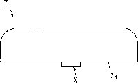
图4是用于描述形成在金属盖子上的凸出部作用的部分截面图;Fig. 4 is a partial cross-sectional view for describing the effect of a protrusion formed on the metal cover;
图5是用于本发明中的导电盖子的另一个较佳实施例的侧视图;Figure 5 is a side view of another preferred embodiment of the conductive cover used in the present invention;
图6是相关技术中的电子部件的分解透视图。Fig. 6 is an exploded perspective view of an electronic component in the related art.
具体实施方式Detailed ways
图1是根据本发明的较佳实施例的电子部件的分解透视图。在本较佳实施例的电子部件中,使用大致上为矩形的壳体基片1。壳体基片1较好地可以由诸如合成树脂之类的绝缘材料,或诸如铝土之类的绝缘陶瓷材料制成。较好地,将端子电极2、3、4和5设置在壳体基片1的上表面上。注意,在端子电极2、3、4和5之间,端子电极3最好接地。较好地,将凹进部分1a、1b和1c设置在壳体基片1的一个侧表面上,并在另一个相对侧的侧表面上形成凹进部分1d、1e和1f。分别将端子电极2的相对的端部设置得延伸到凹进部分1a和1d。端子电极3的相对端部设置得延伸到凹进部分1b和1e。将端子电极4和5的端部设置得延伸到凹进部分1f和1c。FIG. 1 is an exploded perspective view of an electronic component according to a preferred embodiment of the present invention. In the electronic component of this preferred embodiment, a substantially rectangular housing substrate 1 is used. The housing substrate 1 may preferably be made of an insulating material such as synthetic resin, or an insulating ceramic material such as alumina. Preferably, the terminal electrodes 2, 3, 4 and 5 are provided on the upper surface of the housing substrate 1. As shown in FIG. Note that among the terminal electrodes 2, 3, 4 and 5, the terminal electrode 3 is preferably grounded. Preferably, recessed portions 1a, 1b, and 1c are provided on one side surface of the housing substrate 1, and recessed portions 1d, 1e, and 1f are formed on the other side surface on the opposite side. Opposite end portions of the terminal electrodes 2 are arranged to extend to the recessed portions 1a and 1d, respectively. The opposite end portions of the terminal electrodes 3 are arranged to extend to the recessed portions 1b and 1e. The end portions of the terminal electrodes 4 and 5 are arranged to extend to the recessed portions 1f and 1c.
由于将端子电极2、3、4和5设置得分别延伸到凹进部分1a到1f,每一个端子电极2、3、4和5都可以电气连接到一个外部电路,方法是使外部电路连接到凹进部分1a到1f中的一个。在壳体基片1上设置最好大致上为矩形的绝缘层6。绝缘层6设置得防止端子电极2、4和5与金属盖子7之间导电,这将在下面描述。对于绝缘层6的材料没有具体限制,较好地,可以使用诸如环氧树脂或玻璃之类的绝缘材料。Since the terminal electrodes 2, 3, 4 and 5 are arranged to extend respectively to the recessed portions 1a to 1f, each of the terminal electrodes 2, 3, 4 and 5 can be electrically connected to an external circuit by making the external circuit connected to One of the recessed portions 1a to 1f. A preferably substantially rectangular insulating layer 6 is arranged on the housing substrate 1 . The insulating layer 6 is provided to prevent conduction between the terminal electrodes 2, 4 and 5 and the
较好地,将成对的压电元件8和9安装在壳体基片1上。下面将参照图2A和2B描述压电元件的结构。图2A和2B是压电元件8的平面图和仰视图,它们示出了其电极结构。参照图2A和2B,较好地,压电元件8包含细长的大致上为矩形的压电基片10。压电基片10最好由诸如钛酸铅锆陶瓷之类的压电陶瓷材料,或诸如石英之类的压电单晶制成。当压电基片10由压电陶瓷制成时,压电基片10最好沿平行于基片10的主表面的方向极化。Preferably, the paired piezoelectric elements 8 and 9 are mounted on the housing substrate 1 . The structure of the piezoelectric element will be described below with reference to FIGS. 2A and 2B. 2A and 2B are a plan view and a bottom view of the piezoelectric element 8, which show the electrode structure thereof. 2A and 2B, preferably, the piezoelectric element 8 comprises an elongated substantially rectangular piezoelectric substrate 10 . The piezoelectric substrate 10 is preferably made of a piezoelectric ceramic material such as lead zirconium titanate ceramic, or a piezoelectric single crystal such as quartz. When the piezoelectric substrate 10 is made of piezoelectric ceramics, the piezoelectric substrate 10 is preferably polarized in a direction parallel to the main surface of the substrate 10 .
将第一和第二激励电极11和12设置在压电基片10的上表面上,它们之间有预定的间隙。将公共电极13设置在压电基片10的下表面上,从而公共电极13通过压电基片10面对激励电极11和12面对。激励电极11和12与公共电极13构成第一压电谐振部分。First and second excitation electrodes 11 and 12 are provided on the upper surface of the piezoelectric substrate 10 with a predetermined gap therebetween. The common electrode 13 is provided on the lower surface of the piezoelectric substrate 10 so that the common electrode 13 faces the excitation electrodes 11 and 12 through the piezoelectric substrate 10 . The excitation electrodes 11 and 12 and the common electrode 13 constitute a first piezoelectric resonance section.
类似地,将第三和第四激励电极14和15设置在压电基片10的上表面上,它们之间有预定的间隙,并在压电基片10的下表面上确定一个公共电极16,从而公共电极16通过压电基片10面对激励电极14和15。激励电极14和15以及公共电极16构成第二压电谐振部分。Similarly, the third and fourth excitation electrodes 14 and 15 are arranged on the upper surface of the piezoelectric substrate 10 with a predetermined gap therebetween, and a common electrode 16 is defined on the lower surface of the piezoelectric substrate 10. , so that the common electrode 16 faces the excitation electrodes 14 and 15 through the piezoelectric substrate 10 . The excitation electrodes 14 and 15 and the common electrode 16 constitute a second piezoelectric resonance section.
另外,在第二和第三激励电极12和14之间设置电容器电极17,并在压电基片10的下表面上设置另一个电容器电极18。In addition, a capacitor electrode 17 is provided between the second and third excitation electrodes 12 and 14, and another capacitor electrode 18 is provided on the lower surface of the piezoelectric substrate 10.
将第一激励电极11电气连接到沿压电基片10的一个端面设置的端子电极19。类似的,将第四激励电极15电气连接到沿压电基片10的另一个端面设置的端子电极20。将每一个端子电极19和20设置得通过相应的端表面延伸到压电基片10的下表面。注意,压电元件9较好地具有和压电元件8相同的结构。The first excitation electrode 11 is electrically connected to a terminal electrode 19 provided along one end face of the piezoelectric substrate 10 . Similarly, the fourth excitation electrode 15 is electrically connected to the terminal electrode 20 provided along the other end face of the piezoelectric substrate 10 . Each of the terminal electrodes 19 and 20 is arranged to extend to the lower surface of the piezoelectric substrate 10 through the corresponding end surface. Note that piezoelectric element 9 preferably has the same structure as piezoelectric element 8 .
端子电极19和20与电容器电极18之间的电气连接使每一个压电元件8和9能够用作利用厚度切向振动模式的压电滤波器。另外,通过压电元件8的端子电极19与压电元件9的端子电极19之间的电气连接,产生二级压电滤波器。在使用二级压电滤波器中,将输入信号施加给压电元件8的端子电极20,并将压电元件8和9的电容器电极18接地。由此,可以从压电元件9的端子电极20得到输出信号。The electrical connection between the terminal electrodes 19 and 20 and the capacitor electrode 18 enables each of the piezoelectric elements 8 and 9 to function as a piezoelectric filter utilizing the thickness tangential vibration mode. In addition, a two-stage piezoelectric filter is produced by electrical connection between the terminal electrode 19 of the piezoelectric element 8 and the terminal electrode 19 of the piezoelectric element 9 . In using a two-stage piezoelectric filter, an input signal is applied to the terminal electrode 20 of the piezoelectric element 8, and the capacitor electrodes 18 of the piezoelectric elements 8 and 9 are grounded. Thus, an output signal can be obtained from the terminal electrode 20 of the piezoelectric element 9 .
注意,将压电元件8和9电气连接到上述端子电极2到5。现在参照图1,将压电元件8较好地通过导电膏层21、22和23连接到端子电极2、3和4。更具体地说,将端子电极19延伸到压电基片10的下表面的部分通过导电膏层21电气连接到壳体基片1的终端电极2。电容器电极18通过导电膏层22电气连接到壳体基片1的终端电极3。将端子电极20延伸到压电基片10的下表面的部分通过导电膏层23电气连接到壳体基片1的端子电极4。类似地,将压电元件9通过导电膏层24、25和26连接到端子电极2、3和5。Note that the piezoelectric elements 8 and 9 are electrically connected to the above-mentioned terminal electrodes 2 to 5 . Referring now to FIG. 1, the piezoelectric element 8 is preferably connected to the terminal electrodes 2, 3 and 4 through layers 21, 22 and 23 of conductive paste. More specifically, the portion extending the terminal electrode 19 to the lower surface of the piezoelectric substrate 10 is electrically connected to the terminal electrode 2 of the housing substrate 1 through the conductive paste layer 21 . The capacitor electrode 18 is electrically connected to the terminal electrode 3 of the case substrate 1 through the conductive paste layer 22 . Portions extending the terminal electrodes 20 to the lower surface of the piezoelectric substrate 10 are electrically connected to the terminal electrodes 4 of the case substrate 1 through the conductive paste layer 23 . Similarly, the piezoelectric element 9 is connected to the terminal electrodes 2 , 3 and 5 through the conductive paste layers 24 , 25 and 26 .
在将压电元件8和9通过导电膏层21到26连接到壳体基片1后,将导电膏层27和28设置到绝缘层6上。最好将导电膏层27和28设置得跨越绝缘层6,以便建立与端子电极3的电气连接。换句话说,将导电膏层27和28的内端和外端都电气连接到端子电极3。注意,可以将通孔设置在绝缘层6中,以便建立导电膏层27和28与端子电极3之间的电气连接。当将金属盖子7连接到壳体基片1时,首先将导电膏层27和28设置在绝缘层6上,然后将绝缘粘剂29施加到金属盖子7的开口边缘,然后将金属盖子7连接到壳体基片1。金属盖子7的开口边缘最好具有有多个侧边的多边形形状。开口边缘位于较长侧7a和7b的部分最好朝下相对于较短侧7c和7d凸出,从而确定根据本发明的较佳实施例的凸出部X。即,如图3的侧视图所示,较长侧7的中间部分最好朝下凸出以提供凸出部X。注意,在图3中,以夸张的方式描述凸出部,从而图3中凸出部X的凸出量要大于实际的凸出量。After the piezoelectric elements 8 and 9 are connected to the case substrate 1 through the conductive paste layers 21 to 26 , the conductive paste layers 27 and 28 are provided on the insulating layer 6 . The conductive paste layers 27 and 28 are preferably provided across the insulating layer 6 in order to establish electrical connection with the terminal electrodes 3 . In other words, both the inner and outer ends of the conductive paste layers 27 and 28 are electrically connected to the terminal electrodes 3 . Note that via holes may be provided in insulating layer 6 in order to establish electrical connection between conductive paste layers 27 and 28 and terminal electrodes 3 . When the
由于凸出部X,当如图1所示将金属盖子7通过绝缘粘剂连接到壳体基片1的绝缘层6上时,如图4所示,金属盖子7的凸出部X以可靠的方式与导电膏层接触,从而在金属盖子7和端子电极3之间建立了可靠的电气连接。Due to the protrusion X, when the
结果,即使当壳体基片1被弯曲,或绝缘粘剂29被不均匀地施加到金属盖子7时,由于上述金属盖子7的凸出部X,当金属盖子7被压在绝缘层6上时,它可靠地接触导电膏层27和28,该部分和金属盖子7的其它部分相比,更加容易和可靠地与导电膏层27和28接触。相应地,不但可靠安全地实现了金属盖子7与绝缘层6之间的机械连接,还可靠安全地实现了金属盖子7与端子电极3之间的电气连接。由此,金属盖子7可以以可靠的方式提供电磁屏蔽。As a result, even when the case substrate 1 is bent, or the insulating adhesive 29 is unevenly applied to the
在上述较佳实施例中,金属盖子7的开口边缘的每一个较长侧7a和7b的差不多整个部分(但不是全部)都朝下凸出以提供凸出部X。但是,如图5的侧视图所示,较长侧7a和7b的每一侧的中间部分都可以局部朝下凸出,以提供一个凸出部X。或者,较长侧7a和7b的每一个侧边的整个部分可以朝下凸出以提供凸出部X。另外,金属盖子7的开口边缘的形状不限于大致上矩形形状,可以是诸如五边形、圆形或其它适当的形状。还有,可以使用由陶瓷材料制成并覆盖有导电材料的导电盖子替代金属盖子7。注意,设置在导电盖子的开口边缘上的凸出部的位置可以根据壳体基片上接地的端子电极的位置,以及设置得连接到端子电极的导电膏层的位置适当地确定。In the above preferred embodiment, almost the entire part (but not all) of each
虽然已经参照本发明的较佳实施例具体示出和描述了本发明,熟悉本领域的人知道,在不背离本发明的主旨和范围的条件下,可以有上述和其它形式上和细节上的改变。Although the present invention has been particularly shown and described with reference to the preferred embodiments of the present invention, those skilled in the art will understand that the above and other changes in form and details may be made without departing from the spirit and scope of the present invention. Change.
Claims (19)
Applications Claiming Priority (2)
| Application Number | Priority Date | Filing Date | Title |
|---|---|---|---|
| JP070498/1999 | 1999-03-16 | ||
| JP07049899A JP3646776B2 (en) | 1999-03-16 | 1999-03-16 | Electronic components |
Publications (2)
| Publication Number | Publication Date |
|---|---|
| CN1267131A CN1267131A (en) | 2000-09-20 |
| CN1151602C true CN1151602C (en) | 2004-05-26 |
Family
ID=13433259
Family Applications (1)
| Application Number | Title | Priority Date | Filing Date |
|---|---|---|---|
| CNB001043102A Expired - Lifetime CN1151602C (en) | 1999-03-16 | 2000-03-15 | electronic components |
Country Status (3)
| Country | Link |
|---|---|
| JP (1) | JP3646776B2 (en) |
| CN (1) | CN1151602C (en) |
| DE (1) | DE10003501C2 (en) |
Families Citing this family (6)
| Publication number | Priority date | Publication date | Assignee | Title |
|---|---|---|---|---|
| JP3762313B2 (en) * | 2002-02-27 | 2006-04-05 | 富士通株式会社 | Metal enclosure |
| JP4752875B2 (en) * | 2008-06-25 | 2011-08-17 | ソニー株式会社 | Drive device and track jump method |
| JP5463173B2 (en) * | 2010-03-12 | 2014-04-09 | 日立オートモティブシステムズ株式会社 | Angular velocity detector |
| KR20130058956A (en) * | 2011-11-28 | 2013-06-05 | 삼성전기주식회사 | Ultrasonic sensor and manufacturing method thereof |
| TWI656543B (en) * | 2015-10-16 | 2019-04-11 | 日商村田製作所股份有限公司 | Electronic parts |
| KR102653201B1 (en) * | 2016-03-30 | 2024-04-01 | 삼성전기주식회사 | Acoustic wave device and manufacturing method thereof |
Family Cites Families (2)
| Publication number | Priority date | Publication date | Assignee | Title |
|---|---|---|---|---|
| JPH06291594A (en) * | 1993-03-31 | 1994-10-18 | Matsushita Electric Ind Co Ltd | Electronic part and manufacture of the same |
| JP3183169B2 (en) * | 1996-05-09 | 2001-07-03 | 株式会社村田製作所 | Electronic component manufacturing method |
-
1999
- 1999-03-16 JP JP07049899A patent/JP3646776B2/en not_active Expired - Lifetime
-
2000
- 2000-01-27 DE DE2000103501 patent/DE10003501C2/en not_active Expired - Lifetime
- 2000-03-15 CN CNB001043102A patent/CN1151602C/en not_active Expired - Lifetime
Also Published As
| Publication number | Publication date |
|---|---|
| JP2000269772A (en) | 2000-09-29 |
| DE10003501A1 (en) | 2000-10-12 |
| DE10003501C2 (en) | 2003-04-24 |
| CN1267131A (en) | 2000-09-20 |
| JP3646776B2 (en) | 2005-05-11 |
Similar Documents
| Publication | Publication Date | Title |
|---|---|---|
| CN1041681C (en) | crystal oscillator | |
| CN1160787C (en) | Encapsulation for electronic components | |
| CN1140052C (en) | electronic components | |
| US4323865A (en) | Ladder-type piezoelectric filter | |
| CN1217608A (en) | electronic components | |
| CN1170365C (en) | Surface Mount Electronic Components | |
| CN1151602C (en) | electronic components | |
| CN1147938C (en) | Surface mount structures and surface mount electronic components contained therein | |
| US7126260B2 (en) | Surface mount crystal unit | |
| CN1220390A (en) | Infrared sensor | |
| CN1151600C (en) | Piezoelectric element | |
| CN1150621C (en) | Substrate for mounting electronic components and piezoelectric resonant element using the same | |
| JP2001237665A (en) | Surface mount container and crystal resonator using the same | |
| EP1100195B1 (en) | Lead terminal and electronic component including lead terminal | |
| JPS59119911A (en) | piezoelectric vibrator | |
| CN1114990C (en) | Piezoelectric resonator and piezoelectric element containing same | |
| JP2004031787A (en) | Surface mount type electronic device | |
| KR20000071798A (en) | Piezoelectric device and piezoelectric oscillator using the same | |
| JPH11261364A (en) | Electronic component | |
| JP2001036376A (en) | Piezoelectric resonator and piezoelectric component | |
| CN1235411A (en) | Ladder piezoelectric filter | |
| JP2003224221A (en) | Electronic component | |
| JPH0779029A (en) | Piezoelectric transformer | |
| US6376970B1 (en) | Piezoelectric resonator supporting structure and a piezoelectric component including the same | |
| JP2000049556A (en) | Capacitance included piezo-resonator |
Legal Events
| Date | Code | Title | Description |
|---|---|---|---|
| C10 | Entry into substantive examination | ||
| SE01 | Entry into force of request for substantive examination | ||
| C06 | Publication | ||
| PB01 | Publication | ||
| C14 | Grant of patent or utility model | ||
| GR01 | Patent grant | ||
| CX01 | Expiry of patent term |
Granted publication date: 20040526 |
|
| CX01 | Expiry of patent term |