CN115148093A - Electronic product and display device - Google Patents
Electronic product and display device Download PDFInfo
- Publication number
- CN115148093A CN115148093A CN202210250815.XA CN202210250815A CN115148093A CN 115148093 A CN115148093 A CN 115148093A CN 202210250815 A CN202210250815 A CN 202210250815A CN 115148093 A CN115148093 A CN 115148093A
- Authority
- CN
- China
- Prior art keywords
- mpa
- adhesive layer
- storage modulus
- display device
- layer
- Prior art date
- Legal status (The legal status is an assumption and is not a legal conclusion. Google has not performed a legal analysis and makes no representation as to the accuracy of the status listed.)
- Pending
Links
Images


Classifications
-
- G—PHYSICS
- G09—EDUCATION; CRYPTOGRAPHY; DISPLAY; ADVERTISING; SEALS
- G09F—DISPLAYING; ADVERTISING; SIGNS; LABELS OR NAME-PLATES; SEALS
- G09F9/00—Indicating arrangements for variable information in which the information is built-up on a support by selection or combination of individual elements
- G09F9/30—Indicating arrangements for variable information in which the information is built-up on a support by selection or combination of individual elements in which the desired character or characters are formed by combining individual elements
- G09F9/301—Indicating arrangements for variable information in which the information is built-up on a support by selection or combination of individual elements in which the desired character or characters are formed by combining individual elements flexible foldable or roll-able electronic displays, e.g. thin LCD, OLED
-
- G—PHYSICS
- G06—COMPUTING OR CALCULATING; COUNTING
- G06F—ELECTRIC DIGITAL DATA PROCESSING
- G06F3/00—Input arrangements for transferring data to be processed into a form capable of being handled by the computer; Output arrangements for transferring data from processing unit to output unit, e.g. interface arrangements
- G06F3/01—Input arrangements or combined input and output arrangements for interaction between user and computer
- G06F3/03—Arrangements for converting the position or the displacement of a member into a coded form
- G06F3/041—Digitisers, e.g. for touch screens or touch pads, characterised by the transducing means
- G06F3/0412—Digitisers structurally integrated in a display
-
- B—PERFORMING OPERATIONS; TRANSPORTING
- B32—LAYERED PRODUCTS
- B32B—LAYERED PRODUCTS, i.e. PRODUCTS BUILT-UP OF STRATA OF FLAT OR NON-FLAT, e.g. CELLULAR OR HONEYCOMB, FORM
- B32B15/00—Layered products comprising a layer of metal
- B32B15/04—Layered products comprising a layer of metal comprising metal as the main or only constituent of a layer, which is next to another layer of the same or of a different material
- B32B15/06—Layered products comprising a layer of metal comprising metal as the main or only constituent of a layer, which is next to another layer of the same or of a different material of natural rubber or synthetic rubber
-
- B—PERFORMING OPERATIONS; TRANSPORTING
- B32—LAYERED PRODUCTS
- B32B—LAYERED PRODUCTS, i.e. PRODUCTS BUILT-UP OF STRATA OF FLAT OR NON-FLAT, e.g. CELLULAR OR HONEYCOMB, FORM
- B32B15/00—Layered products comprising a layer of metal
- B32B15/04—Layered products comprising a layer of metal comprising metal as the main or only constituent of a layer, which is next to another layer of the same or of a different material
- B32B15/08—Layered products comprising a layer of metal comprising metal as the main or only constituent of a layer, which is next to another layer of the same or of a different material of synthetic resin
- B32B15/082—Layered products comprising a layer of metal comprising metal as the main or only constituent of a layer, which is next to another layer of the same or of a different material of synthetic resin comprising vinyl resins; comprising acrylic resins
-
- B—PERFORMING OPERATIONS; TRANSPORTING
- B32—LAYERED PRODUCTS
- B32B—LAYERED PRODUCTS, i.e. PRODUCTS BUILT-UP OF STRATA OF FLAT OR NON-FLAT, e.g. CELLULAR OR HONEYCOMB, FORM
- B32B15/00—Layered products comprising a layer of metal
- B32B15/04—Layered products comprising a layer of metal comprising metal as the main or only constituent of a layer, which is next to another layer of the same or of a different material
- B32B15/08—Layered products comprising a layer of metal comprising metal as the main or only constituent of a layer, which is next to another layer of the same or of a different material of synthetic resin
- B32B15/095—Layered products comprising a layer of metal comprising metal as the main or only constituent of a layer, which is next to another layer of the same or of a different material of synthetic resin comprising polyurethanes
-
- B—PERFORMING OPERATIONS; TRANSPORTING
- B32—LAYERED PRODUCTS
- B32B—LAYERED PRODUCTS, i.e. PRODUCTS BUILT-UP OF STRATA OF FLAT OR NON-FLAT, e.g. CELLULAR OR HONEYCOMB, FORM
- B32B15/00—Layered products comprising a layer of metal
- B32B15/18—Layered products comprising a layer of metal comprising iron or steel
-
- B—PERFORMING OPERATIONS; TRANSPORTING
- B32—LAYERED PRODUCTS
- B32B—LAYERED PRODUCTS, i.e. PRODUCTS BUILT-UP OF STRATA OF FLAT OR NON-FLAT, e.g. CELLULAR OR HONEYCOMB, FORM
- B32B25/00—Layered products comprising a layer of natural or synthetic rubber
- B32B25/04—Layered products comprising a layer of natural or synthetic rubber comprising rubber as the main or only constituent of a layer, which is next to another layer of the same or of a different material
- B32B25/08—Layered products comprising a layer of natural or synthetic rubber comprising rubber as the main or only constituent of a layer, which is next to another layer of the same or of a different material of synthetic resin
-
- B—PERFORMING OPERATIONS; TRANSPORTING
- B32—LAYERED PRODUCTS
- B32B—LAYERED PRODUCTS, i.e. PRODUCTS BUILT-UP OF STRATA OF FLAT OR NON-FLAT, e.g. CELLULAR OR HONEYCOMB, FORM
- B32B27/00—Layered products comprising a layer of synthetic resin
- B32B27/06—Layered products comprising a layer of synthetic resin as the main or only constituent of a layer, which is next to another layer of the same or of a different material
- B32B27/08—Layered products comprising a layer of synthetic resin as the main or only constituent of a layer, which is next to another layer of the same or of a different material of synthetic resin
-
- B—PERFORMING OPERATIONS; TRANSPORTING
- B32—LAYERED PRODUCTS
- B32B—LAYERED PRODUCTS, i.e. PRODUCTS BUILT-UP OF STRATA OF FLAT OR NON-FLAT, e.g. CELLULAR OR HONEYCOMB, FORM
- B32B27/00—Layered products comprising a layer of synthetic resin
- B32B27/30—Layered products comprising a layer of synthetic resin comprising vinyl (co)polymers; comprising acrylic (co)polymers
- B32B27/308—Layered products comprising a layer of synthetic resin comprising vinyl (co)polymers; comprising acrylic (co)polymers comprising acrylic (co)polymers
-
- B—PERFORMING OPERATIONS; TRANSPORTING
- B32—LAYERED PRODUCTS
- B32B—LAYERED PRODUCTS, i.e. PRODUCTS BUILT-UP OF STRATA OF FLAT OR NON-FLAT, e.g. CELLULAR OR HONEYCOMB, FORM
- B32B27/00—Layered products comprising a layer of synthetic resin
- B32B27/36—Layered products comprising a layer of synthetic resin comprising polyesters
-
- B—PERFORMING OPERATIONS; TRANSPORTING
- B32—LAYERED PRODUCTS
- B32B—LAYERED PRODUCTS, i.e. PRODUCTS BUILT-UP OF STRATA OF FLAT OR NON-FLAT, e.g. CELLULAR OR HONEYCOMB, FORM
- B32B27/00—Layered products comprising a layer of synthetic resin
- B32B27/40—Layered products comprising a layer of synthetic resin comprising polyurethanes
-
- B—PERFORMING OPERATIONS; TRANSPORTING
- B32—LAYERED PRODUCTS
- B32B—LAYERED PRODUCTS, i.e. PRODUCTS BUILT-UP OF STRATA OF FLAT OR NON-FLAT, e.g. CELLULAR OR HONEYCOMB, FORM
- B32B3/00—Layered products comprising a layer with external or internal discontinuities or unevennesses, or a layer of non-planar shape; Layered products comprising a layer having particular features of form
- B32B3/02—Layered products comprising a layer with external or internal discontinuities or unevennesses, or a layer of non-planar shape; Layered products comprising a layer having particular features of form characterised by features of form at particular places, e.g. in edge regions
- B32B3/08—Layered products comprising a layer with external or internal discontinuities or unevennesses, or a layer of non-planar shape; Layered products comprising a layer having particular features of form characterised by features of form at particular places, e.g. in edge regions characterised by added members at particular parts
- B32B3/085—Layered products comprising a layer with external or internal discontinuities or unevennesses, or a layer of non-planar shape; Layered products comprising a layer having particular features of form characterised by features of form at particular places, e.g. in edge regions characterised by added members at particular parts spaced apart pieces on the surface of a layer
-
- B—PERFORMING OPERATIONS; TRANSPORTING
- B32—LAYERED PRODUCTS
- B32B—LAYERED PRODUCTS, i.e. PRODUCTS BUILT-UP OF STRATA OF FLAT OR NON-FLAT, e.g. CELLULAR OR HONEYCOMB, FORM
- B32B7/00—Layered products characterised by the relation between layers; Layered products characterised by the relative orientation of features between layers, or by the relative values of a measurable parameter between layers, i.e. products comprising layers having different physical, chemical or physicochemical properties; Layered products characterised by the interconnection of layers
- B32B7/04—Interconnection of layers
- B32B7/12—Interconnection of layers using interposed adhesives or interposed materials with bonding properties
-
- C—CHEMISTRY; METALLURGY
- C09—DYES; PAINTS; POLISHES; NATURAL RESINS; ADHESIVES; COMPOSITIONS NOT OTHERWISE PROVIDED FOR; APPLICATIONS OF MATERIALS NOT OTHERWISE PROVIDED FOR
- C09J—ADHESIVES; NON-MECHANICAL ASPECTS OF ADHESIVE PROCESSES IN GENERAL; ADHESIVE PROCESSES NOT PROVIDED FOR ELSEWHERE; USE OF MATERIALS AS ADHESIVES
- C09J11/00—Features of adhesives not provided for in group C09J9/00, e.g. additives
- C09J11/02—Non-macromolecular additives
- C09J11/06—Non-macromolecular additives organic
-
- C—CHEMISTRY; METALLURGY
- C09—DYES; PAINTS; POLISHES; NATURAL RESINS; ADHESIVES; COMPOSITIONS NOT OTHERWISE PROVIDED FOR; APPLICATIONS OF MATERIALS NOT OTHERWISE PROVIDED FOR
- C09J—ADHESIVES; NON-MECHANICAL ASPECTS OF ADHESIVE PROCESSES IN GENERAL; ADHESIVE PROCESSES NOT PROVIDED FOR ELSEWHERE; USE OF MATERIALS AS ADHESIVES
- C09J183/00—Adhesives based on macromolecular compounds obtained by reactions forming in the main chain of the macromolecule a linkage containing silicon, with or without sulfur, nitrogen, oxygen, or carbon only; Adhesives based on derivatives of such polymers
- C09J183/04—Polysiloxanes
- C09J183/06—Polysiloxanes containing silicon bound to oxygen-containing groups
-
- G—PHYSICS
- G06—COMPUTING OR CALCULATING; COUNTING
- G06F—ELECTRIC DIGITAL DATA PROCESSING
- G06F3/00—Input arrangements for transferring data to be processed into a form capable of being handled by the computer; Output arrangements for transferring data from processing unit to output unit, e.g. interface arrangements
- G06F3/01—Input arrangements or combined input and output arrangements for interaction between user and computer
- G06F3/03—Arrangements for converting the position or the displacement of a member into a coded form
- G06F3/041—Digitisers, e.g. for touch screens or touch pads, characterised by the transducing means
- G06F3/046—Digitisers, e.g. for touch screens or touch pads, characterised by the transducing means by electromagnetic means
-
- H—ELECTRICITY
- H10—SEMICONDUCTOR DEVICES; ELECTRIC SOLID-STATE DEVICES NOT OTHERWISE PROVIDED FOR
- H10K—ORGANIC ELECTRIC SOLID-STATE DEVICES
- H10K77/00—Constructional details of devices covered by this subclass and not covered by groups H10K10/80, H10K30/80, H10K50/80 or H10K59/80
- H10K77/10—Substrates, e.g. flexible substrates
- H10K77/111—Flexible substrates
-
- B—PERFORMING OPERATIONS; TRANSPORTING
- B32—LAYERED PRODUCTS
- B32B—LAYERED PRODUCTS, i.e. PRODUCTS BUILT-UP OF STRATA OF FLAT OR NON-FLAT, e.g. CELLULAR OR HONEYCOMB, FORM
- B32B2255/00—Coating on the layer surface
- B32B2255/26—Polymeric coating
-
- B—PERFORMING OPERATIONS; TRANSPORTING
- B32—LAYERED PRODUCTS
- B32B—LAYERED PRODUCTS, i.e. PRODUCTS BUILT-UP OF STRATA OF FLAT OR NON-FLAT, e.g. CELLULAR OR HONEYCOMB, FORM
- B32B2307/00—Properties of the layers or laminate
- B32B2307/40—Properties of the layers or laminate having particular optical properties
- B32B2307/42—Polarizing, birefringent, filtering
-
- B—PERFORMING OPERATIONS; TRANSPORTING
- B32—LAYERED PRODUCTS
- B32B—LAYERED PRODUCTS, i.e. PRODUCTS BUILT-UP OF STRATA OF FLAT OR NON-FLAT, e.g. CELLULAR OR HONEYCOMB, FORM
- B32B2307/00—Properties of the layers or laminate
- B32B2307/50—Properties of the layers or laminate having particular mechanical properties
- B32B2307/56—Damping, energy absorption
-
- B—PERFORMING OPERATIONS; TRANSPORTING
- B32—LAYERED PRODUCTS
- B32B—LAYERED PRODUCTS, i.e. PRODUCTS BUILT-UP OF STRATA OF FLAT OR NON-FLAT, e.g. CELLULAR OR HONEYCOMB, FORM
- B32B2307/00—Properties of the layers or laminate
- B32B2307/50—Properties of the layers or laminate having particular mechanical properties
- B32B2307/584—Scratch resistance
-
- B—PERFORMING OPERATIONS; TRANSPORTING
- B32—LAYERED PRODUCTS
- B32B—LAYERED PRODUCTS, i.e. PRODUCTS BUILT-UP OF STRATA OF FLAT OR NON-FLAT, e.g. CELLULAR OR HONEYCOMB, FORM
- B32B2457/00—Electrical equipment
- B32B2457/20—Displays, e.g. liquid crystal displays, plasma displays
- B32B2457/208—Touch screens
-
- C—CHEMISTRY; METALLURGY
- C09—DYES; PAINTS; POLISHES; NATURAL RESINS; ADHESIVES; COMPOSITIONS NOT OTHERWISE PROVIDED FOR; APPLICATIONS OF MATERIALS NOT OTHERWISE PROVIDED FOR
- C09J—ADHESIVES; NON-MECHANICAL ASPECTS OF ADHESIVE PROCESSES IN GENERAL; ADHESIVE PROCESSES NOT PROVIDED FOR ELSEWHERE; USE OF MATERIALS AS ADHESIVES
- C09J2203/00—Applications of adhesives in processes or use of adhesives in the form of films or foils
- C09J2203/326—Applications of adhesives in processes or use of adhesives in the form of films or foils for bonding electronic components such as wafers, chips or semiconductors
-
- G—PHYSICS
- G06—COMPUTING OR CALCULATING; COUNTING
- G06F—ELECTRIC DIGITAL DATA PROCESSING
- G06F2203/00—Indexing scheme relating to G06F3/00 - G06F3/048
- G06F2203/041—Indexing scheme relating to G06F3/041 - G06F3/045
- G06F2203/04102—Flexible digitiser, i.e. constructional details for allowing the whole digitising part of a device to be flexed or rolled like a sheet of paper
-
- G—PHYSICS
- G06—COMPUTING OR CALCULATING; COUNTING
- G06F—ELECTRIC DIGITAL DATA PROCESSING
- G06F2203/00—Indexing scheme relating to G06F3/00 - G06F3/048
- G06F2203/041—Indexing scheme relating to G06F3/041 - G06F3/045
- G06F2203/04103—Manufacturing, i.e. details related to manufacturing processes specially suited for touch sensitive devices
-
- H—ELECTRICITY
- H10—SEMICONDUCTOR DEVICES; ELECTRIC SOLID-STATE DEVICES NOT OTHERWISE PROVIDED FOR
- H10K—ORGANIC ELECTRIC SOLID-STATE DEVICES
- H10K2102/00—Constructional details relating to the organic devices covered by this subclass
- H10K2102/301—Details of OLEDs
- H10K2102/311—Flexible OLED
-
- H—ELECTRICITY
- H10—SEMICONDUCTOR DEVICES; ELECTRIC SOLID-STATE DEVICES NOT OTHERWISE PROVIDED FOR
- H10K—ORGANIC ELECTRIC SOLID-STATE DEVICES
- H10K59/00—Integrated devices, or assemblies of multiple devices, comprising at least one organic light-emitting element covered by group H10K50/00
- H10K59/40—OLEDs integrated with touch screens
Landscapes
- Engineering & Computer Science (AREA)
- Theoretical Computer Science (AREA)
- Physics & Mathematics (AREA)
- General Engineering & Computer Science (AREA)
- General Physics & Mathematics (AREA)
- Human Computer Interaction (AREA)
- Chemical & Material Sciences (AREA)
- Organic Chemistry (AREA)
- Electromagnetism (AREA)
- Chemical Kinetics & Catalysis (AREA)
- Laminated Bodies (AREA)
- Liquid Crystal (AREA)
Abstract
本申请涉及包括折叠区域和非折叠区域的显示装置。所述显示装置包括显示面板和前堆叠结构。所述显示面板具有前表面。所述显示面板被配置成在所述前表面上显示图像。所述前堆叠结构设置在所述显示面板的所述前表面上。所述前堆叠结构包括跨所述折叠区域和所述非折叠区域设置的粘合剂层。所述粘合剂层包含紫外可固化粘合剂。所述紫外可固化粘合剂包括乙烯基硅烷和氢硅烷。所述粘合剂层在‑20℃至25℃的温度范围内具有0.05MPa至0.3MPa的储能模量。

The present application relates to a display device including a folded area and an unfolded area. The display device includes a display panel and a front stack structure. The display panel has a front surface. The display panel is configured to display an image on the front surface. The front stack structure is disposed on the front surface of the display panel. The front stack structure includes an adhesive layer disposed across the folded area and the unfolded area. The adhesive layer includes a UV-curable adhesive. The UV-curable adhesive includes vinylsilane and hydrosilane. The adhesive layer has a storage modulus of 0.05 MPa to 0.3 MPa in a temperature range of -20°C to 25°C.
Description
技术领域technical field
实施方案一般地涉及电子产品和显示装置。Embodiments generally relate to electronic products and display devices.
背景技术Background technique
电子产品和显示装置可以包括各种组件,并且使用粘合剂来结合这些组件。粘合剂可以以粘合剂层、粘合剂片、粘合剂膜等的形式提供,并且可以基于粘合机理分为各种类型的粘合剂。例如,粘合剂包括其中粘合剂材料通过压力起作用的压敏粘合剂(PSA)、通过热量固化的热固性粘合剂、通过光能固化的可光固化粘合剂等。Electronic products and display devices may include various components, and adhesives are used to bond these components. The adhesive may be provided in the form of an adhesive layer, an adhesive sheet, an adhesive film, and the like, and may be classified into various types of adhesives based on an adhesive mechanism. For example, adhesives include pressure sensitive adhesives (PSAs) in which the adhesive material is actuated by pressure, thermosetting adhesives cured by heat, photocurable adhesives cured by light energy, and the like.
粘合剂的期望物理性质可以根据使用电子产品和显示装置的环境和其特性而变化。例如,在设计成可变形的电子产品的情况下,设置储能模量以适应反复变形并且避免永久变形是有利的。The desired physical properties of the adhesive may vary depending on the environment in which the electronic product and display device are used and its characteristics. For example, in the case of electronic products designed to be deformable, it is advantageous to set the storage modulus to accommodate repeated deformation and avoid permanent deformation.
本章节中公开的以上信息仅用于理解本发明构思的背景,并且因此可以含有不构成现有技术的信息。The above information disclosed in this section is only for background of understanding of the inventive concept and therefore may contain information that does not form prior art.
发明内容SUMMARY OF THE INVENTION
一些方面提供了包含能够反复变形但防止其永久变形的粘合剂的电子产品。Some aspects provide electronic products comprising adhesives capable of repeated deformation but preventing permanent deformation thereof.
一些方面提供了包含能够反复变形但防止其永久变形的粘合剂的显示装置。Some aspects provide a display device that includes an adhesive capable of being repeatedly deformed but preventing permanent deformation.
其它方面将在以下详细描述中阐述,并且在某种程度上根据公开内容将是显而易见的,或者可以通过本发明构思的实践而获悉。Other aspects will be set forth in the following detailed description, and to the extent that will be apparent from the disclosure, or may be learned by practice of the inventive concepts.
根据一些实施方案,显示装置包括折叠区域和非折叠区域。所述显示装置包括显示面板和前堆叠结构。所述显示面板具有前表面。所述显示面板被配置成在所述前表面上显示图像。所述前堆叠结构设置在所述显示面板的所述前表面上。所述前堆叠结构包括跨所述折叠区域和所述非折叠区域设置的粘合剂层。所述粘合剂层包含紫外可固化粘合剂。所述紫外可固化粘合剂包括乙烯基硅烷和氢硅烷(hydrosilane)。所述粘合剂层在-20℃至25℃的温度范围内具有0.05MPa至0.3MPa的储能模量。According to some embodiments, the display device includes a folded area and an unfolded area. The display device includes a display panel and a front stack structure. The display panel has a front surface. The display panel is configured to display an image on the front surface. The front stack structure is disposed on the front surface of the display panel. The front stack structure includes an adhesive layer disposed across the folded area and the unfolded area. The adhesive layer includes a UV-curable adhesive. The UV-curable adhesive includes vinylsilane and hydrosilane. The adhesive layer has a storage modulus of 0.05 MPa to 0.3 MPa in a temperature range of -20°C to 25°C.
根据一些实施方案,显示装置包括显示面板、第一上部覆盖构件、第二上部覆盖构件、第三上部覆盖构件、第一下部覆盖构件、第二下部覆盖构件、第三下部覆盖构件、第一结合层、第二结合层、第三结合层、第四结合层、第五结合层和第六结合层。所述第一上部覆盖构件设置在所述显示面板上。所述第二上部覆盖构件设置在所述第一上部覆盖构件上。所述第三上部覆盖构件设置在所述第二上部覆盖构件上。所述第一下部覆盖构件设置在所述显示面板下。所述第二下部覆盖构件设置在所述第一下部覆盖构件下。所述第三下部覆盖构件设置在所述第二下部覆盖构件下。所述第一结合层设置在所述第三上部覆盖构件与所述第二上部覆盖构件之间。所述第二结合层设置在所述第二上部覆盖构件与所述第一上部覆盖构件之间。所述第三结合层设置在所述第一上部覆盖构件与所述显示面板之间。所述第四结合层设置在所述显示面板与所述第一下部覆盖构件之间。所述第五结合层设置在所述第一下部覆盖构件与所述第二下部覆盖构件之间。所述第六结合层设置在所述第二下部覆盖构件与所述第三下部覆盖构件之间。所述第一结合层和所述第二结合层中的每一个是紫外可固化层。所述第一结合层和所述第二结合层中的每一个具有在-20℃下的0.08MPa至0.3MPa的储能模量和在25℃下的0.05MPa至0.2MPa的储能模量。According to some embodiments, a display device includes a display panel, a first upper cover member, a second upper cover member, a third upper cover member, a first lower cover member, a second lower cover member, a third lower cover member, a first A bonding layer, a second bonding layer, a third bonding layer, a fourth bonding layer, a fifth bonding layer, and a sixth bonding layer. The first upper cover member is provided on the display panel. The second upper covering member is provided on the first upper covering member. The third upper covering member is provided on the second upper covering member. The first lower cover member is disposed under the display panel. The second lower covering member is disposed under the first lower covering member. The third lower covering member is disposed under the second lower covering member. The first bonding layer is provided between the third upper covering member and the second upper covering member. The second bonding layer is provided between the second upper covering member and the first upper covering member. The third bonding layer is disposed between the first upper cover member and the display panel. The fourth bonding layer is disposed between the display panel and the first lower cover member. The fifth bonding layer is provided between the first lower covering member and the second lower covering member. The sixth bonding layer is provided between the second lower covering member and the third lower covering member. Each of the first bonding layer and the second bonding layer is an ultraviolet curable layer. Each of the first bonding layer and the second bonding layer has a storage modulus of 0.08 MPa to 0.3 MPa at -20°C and a storage modulus of 0.05 MPa to 0.2 MPa at 25°C .
根据一些实施方案,电子产品包括第一结构、第二结构以及插置在所述第一结构与所述第二结构之间以将所述第一结构结合至所述第二结构的粘合剂层。所述粘合剂层包含紫外可固化材料。所述粘合剂层具有在-20℃下的0.08MPa至0.3MPa的储能模量和在25℃下的0.05MPa至0.2MPa的储能模量。According to some embodiments, an electronic product includes a first structure, a second structure, and an adhesive interposed between the first structure and the second structure to bond the first structure to the second structure Floor. The adhesive layer contains an ultraviolet curable material. The adhesive layer has a storage modulus of 0.08 to 0.3 MPa at -20°C and a storage modulus of 0.05 to 0.2 MPa at 25°C.
根据各种实施方案,由于电子产品和/或显示装置包括能够反复变形但防止其永久变形的粘合剂层,因此可以防止粘合剂层的变形被反映到电子产品或显示装置的外部形状中,这否则可能被用户视觉识别到。According to various embodiments, since the electronic product and/or the display device includes the adhesive layer that can be repeatedly deformed but is prevented from being permanently deformed, the deformation of the adhesive layer can be prevented from being reflected in the outer shape of the electronic product or the display device , which might otherwise be visually recognized by the user.
前述一般描述和以下详细描述是示例性且解释性的,并且旨在提供对要求保护的主题的进一步解释。The foregoing general description and the following detailed description are exemplary and explanatory, and are intended to provide further explanation of the claimed subject matter.
附图说明Description of drawings
包括附图以提供对本发明构思的进一步理解以及将附图并入本说明书中并且构成本说明书的一部分,附图例示出本发明构思的实施方案,并且与描述一起用于解释本发明构思的原理。在附图中:The accompanying drawings, which are included to provide a further understanding of the inventive concept and are incorporated in and constitute a part of this specification, illustrate embodiments of the inventive concept and together with the description serve to explain the principle of the inventive concept . In the attached image:
图1是示出根据实施方案的电子产品的横截面视图;1 is a cross-sectional view illustrating an electronic product according to an embodiment;
图2是示出根据实施方案的图1的电子产品的外部形状的变形的横截面视图;2 is a cross-sectional view showing a deformation of the outer shape of the electronic product of FIG. 1 according to an embodiment;
图3是示出根据实施方案的图1的电子产品的外部形状的变形的横截面视图;3 is a cross-sectional view illustrating a deformation of the outer shape of the electronic product of FIG. 1 according to an embodiment;
图4是示出根据实施方案的施加至图1的电子产品的外部压力的横截面视图;4 is a cross-sectional view illustrating external pressure applied to the electronic product of FIG. 1 according to an embodiment;
图5是示出根据各种实施方案的图1的粘合剂层的取决于温度的储能模量的各种实例的图;5 is a graph illustrating various examples of temperature-dependent storage modulus of the adhesive layer of FIG. 1 according to various embodiments;
图6是示出根据实施方案的形成粘合剂层的方法的流程图;6 is a flowchart illustrating a method of forming an adhesive layer according to an embodiment;
图7、图8和图9是例示出根据实施方案的形成粘合剂层的方法的横截面视图;7 , 8 and 9 are cross-sectional views illustrating a method of forming an adhesive layer according to an embodiment;
图10是根据实施方案的显示装置的透视图;10 is a perspective view of a display device according to an embodiment;
图11是示出根据实施方案的图10的显示装置的折叠状态的图;FIG. 11 is a diagram illustrating a folded state of the display device of FIG. 10 according to an embodiment;
图12是示出根据实施方案的图10的显示装置的横截面视图;12 is a cross-sectional view illustrating the display device of FIG. 10 according to an embodiment;
图13是示出根据实施方案的显示面板的横截面视图;13 is a cross-sectional view illustrating a display panel according to an embodiment;
图14是根据实施方案的数字化仪层的分解透视图;14 is an exploded perspective view of a digitizer layer according to an embodiment;
图15是根据实施方案的图14的数字化仪层的横截面视图;以及15 is a cross-sectional view of the digitizer layer of FIG. 14, according to an embodiment; and
图16是根据实施方案的显示装置的横截面视图。16 is a cross-sectional view of a display device according to an embodiment.
具体实施方式Detailed ways
在以下描述中,出于解释的目的,阐述了许多具体细节以提供对各种实施方案的透彻理解。如本文使用,术语“实施方案”和“实施方式”可以互换使用,并且是采用本文公开的发明构思中的一种或多于一种的非限制性实例。然而,显而易见地,各种实施方案可以在没有这些具体细节的情况下实践,或者可以用一种或多于一种的等同布置来实践。在其它情况中,以框图形式示出公知的结构和装置以避免不必要地混淆各种实施方案。此外,各种实施方案可以是不同的,但不必是排它的。例如,在不背离本发明构思的情况下,实施方案的具体形状、配置和特性可以在另一个实施方案中使用或实施。In the following description, for the purposes of explanation, numerous specific details are set forth in order to provide a thorough understanding of various embodiments. As used herein, the terms "embodiment" and "embodiment" are used interchangeably and are non-limiting examples employing one or more of the inventive concepts disclosed herein. It will be apparent, however, that various embodiments may be practiced without these specific details, or with one or more equivalent arrangements. In other instances, well-known structures and devices are shown in block diagram form in order to avoid unnecessarily obscuring the various embodiments. Furthermore, the various embodiments may vary, but are not necessarily exclusive. For example, the specific shapes, configurations and characteristics of an embodiment may be used or implemented in another embodiment without departing from the inventive concept.
除非另外指明,例示的实施方案应被理解为提供一些实施方案的不同细节的示例性特征。因此,除非另外指明,在不背离本发明构思的情况下,各种示例的特征、组件、模块、层、膜、面板、区、方面等(在下文单独地或共同地被称为“元件(element或elements)”)可以以其它方式组合、分离、互换和/或重新布置。Unless otherwise indicated, the illustrated embodiments should be understood to provide exemplary features of various details of some embodiments. Thus, unless otherwise specified, the features, components, modules, layers, films, panels, regions, aspects, etc. of the various examples (hereinafter individually or collectively referred to as "elements ( element or elements)") may be otherwise combined, separated, interchanged and/or rearranged.
通常提供交叉影线和/或阴影在附图中的使用以阐明相邻元件之间的界线。如此,交叉影线或阴影的存在或不存在均不表达或表明对特定材料、材料性质、尺寸、比例、例示的元件之间的共性和/或元件的任何其它特性、属性、性质等的任何偏好或需要,除非指明。此外,在附图中,出于清晰和/或描述性目的,可以放大元件的尺寸和相对尺寸。如此,各个元件的尺寸和相对尺寸不必局限于附图中示出的尺寸和相对尺寸。当实施方案可以不同地实施时,可以与描述的顺序不同地进行具体的过程顺序。例如,两个连续描述的过程可以基本上同时进行或以与描述的顺序相反的顺序进行。此外,相同的参考数字表示相同的元件。The use of cross-hatching and/or hatching in the figures is generally provided to clarify boundaries between adjacent elements. As such, the presence or absence of cross-hatching or shading does not express or imply any representation or indication of any particular material, material properties, dimensions, proportions, commonalities between the illustrated elements and/or any other characteristics, properties, properties, etc. of the elements. preference or need, unless specified. Furthermore, in the drawings, the size and relative sizes of elements may be exaggerated for clarity and/or descriptive purposes. As such, the dimensions and relative dimensions of the various elements are not necessarily limited to those shown in the drawings. When embodiments may be practiced differently, the specific sequence of processes may be performed differently than described. For example, two processes described in succession may be performed substantially concurrently or in the reverse order of the order described. Furthermore, the same reference numerals denote the same elements.
当诸如层的元件被称为在另一个元件“上”、“连接至”另一个元件、或者“联接至”另一个元件时,其可以直接在另一个元件上、直接连接至另一个元件、或者直接联接至另一个元件,或者可以存在介于中间的元件。然而,当元件被称为“直接在”另一个元件“上”、“直接连接至”另一个元件或者“直接联接至”另一个元件时,不存在介于中间的元件。用于描述元件之间的关系的其它术语和/或短语应以类似的方式解释,例如“在......之间”与“直接在......之间”、“相邻”与“直接相邻”、“在......上”与“直接在......上”等。此外,术语“连接的”可以是指物理连接、电连接和/或流体连接。此外,X-轴、Y-轴和Z-轴不局限于直角坐标系的三个轴,并且可以以更广泛的含义解释。例如,X-轴、Y-轴和Z-轴可以彼此垂直,或者可以表示彼此不垂直的不同方向。出于本公开内容的目的,“X、Y和Z中的至少一个(种)”和“选自由X、Y和Z组成的组中的至少一个(种)”可以解释为仅有X、仅有Y、仅有Z,或者X、Y和Z中的两个(种)或多于两个(种)的任意组合,例如,以XYZ、XYY、YZ和ZZ为例。如本文使用,术语“和/或”包括相关列出项中的一个或多于一个的任意组合和所有组合。When an element such as a layer is referred to as being "on," "connected to," or "coupled to" another element, it can be directly on, directly connected to, Either directly coupled to another element, or intervening elements may be present. However, when an element is referred to as being "directly on," "directly connected to," or "directly coupled to" another element, there are no intervening elements present. Other terms and/or phrases used to describe the relationship between elements should be interpreted in a similar fashion, eg, "between" versus "directly between", "phase" "adjacent" versus "directly adjacent", "on" versus "directly on", etc. Additionally, the term "connected" may refer to physical, electrical, and/or fluid connections. Furthermore, the X-axis, Y-axis, and Z-axis are not limited to the three axes of the Cartesian coordinate system, and may be interpreted in a broader sense. For example, the X-axis, Y-axis, and Z-axis may be perpendicular to each other, or may represent different directions that are not perpendicular to each other. For the purposes of this disclosure, "at least one (species) of X, Y, and Z" and "at least one (species) selected from the group consisting of X, Y, and Z" can be interpreted as only X, only There is Y, only Z, or any combination of two (species) or more than two (species) of X, Y, and Z, for example, XYZ, XYY, YZ, and ZZ. As used herein, the term "and/or" includes any and all combinations of one or more of the associated listed items.
尽管术语“第一”、“第二”等可以在本文用于描述各种元件,但这些元件不应受到这些术语限制。这些术语用于区分一个元件与另一个元件。因此,在不背离本公开内容的教导的情况下,以下讨论的第一元件可以被称为第二元件。Although the terms "first," "second," etc. may be used herein to describe various elements, these elements should not be limited by these terms. These terms are used to distinguish one element from another. Thus, a first element discussed below could be termed a second element without departing from the teachings of the present disclosure.
诸如“之下”、“下方”、“下”、“下部”、“上方”、“上”、“之上”、“上部”、“侧”(例如,如在“侧壁”中)等的空间相对术语可以在本文用于描述性目的,并且由此,用于描述如附图中例示的一个元件与另一个元件的关系。空间相对术语旨在涵盖除了附图中描述的方向之外的在使用、操作和/或制造中的设备的不同方向。例如,如果附图中的设备被翻转,被描述为在其它元件或特征“下方”或“之下”的元件则将被定向在其它元件或特征“上方”。因此,术语“下方”可以涵盖上方和下方的方向两者。此外,可以将设备以其它方式定向(例如,旋转90度或在其它方向上),并且如此,本文使用的空间相对描述符被相应地解释。such as "below", "below", "below", "lower", "above", "upper", "above", "upper", "side" (eg, as in "sidewall"), etc. The spatially relative terms of may be used herein for descriptive purposes and, thus, to describe one element's relationship to another element as exemplified in the figures. Spatially relative terms are intended to encompass different orientations of the device in use, operation and/or manufacture in addition to the orientation depicted in the figures. For example, if the device in the figures is turned over, elements described as "below" or "beneath" other elements or features would then be oriented "above" the other elements or features. Thus, the term "below" can encompass both an orientation of above and below. Furthermore, the device may be otherwise oriented (eg, rotated 90 degrees or at other orientations) and, as such, the spatially relative descriptors used herein are to be interpreted accordingly.
本文使用的术语出于描述一些实施方案的目的,而不旨在限制。如本文使用,单数形式“一(a)”、“一(an)”和“所述(the)”旨在还包括复数形式,除非上下文另外明确说明。此外,术语“包含(comprises)”、“包含(comprising)”、“包括(includes)”和/或“包括(including)”当用于本说明书时指明规定的特征、整数、步骤、操作、元件、组件和/或其群组的存在,但不排除一个或多于一个的其它的特征、整数、步骤、操作、元件、组件和/或其群组的存在或增添。还注意,如本文使用,术语“基本上”、“约”和其它类似术语用作近似的术语而不用作程度的术语,并且如此,用于解释本领域普通技术人员会认识到的测量值、计算值和/或提供值中的固有偏差。The terminology used herein is for the purpose of describing some embodiments and is not intended to be limiting. As used herein, the singular forms "a (a)," "an (an)," and "the (the)" are intended to include the plural forms as well, unless the context clearly dictates otherwise. Furthermore, the terms "comprises", "comprising", "includes" and/or "including" when used in this specification designate specified features, integers, steps, operations, elements , components and/or groups thereof, but does not preclude the presence or addition of one or more other features, integers, steps, operations, elements, components and/or groups thereof. Note also that, as used herein, the terms "substantially," "about," and other similar terms are used as terms of approximation and not as terms of degree, and, as such, are used to explain measurements, Inherent bias in calculated values and/or provided values.
本文参考截面视图、等距视图、透视图、平面图和/或分解图示(它们是理想化的实施方案和/或中间结构的示意性图示)描述各种实施方案。如此,应预期由于例如制造技术和/或公差而产生的图示的形状的变化。因此,本文公开的实施方案不应解释为局限于区的具体例示的形状,而应包括由例如制造而产生的形状的偏差。鉴于此,附图中例示的区可以在本质上是示意性的,并且这些区的形状可以不反映装置的区的实际形状,并且如此,不旨在限制。Various embodiments are described herein with reference to cross-sectional, isometric, perspective, plan, and/or exploded illustrations that are schematic illustrations of idealized embodiments and/or intermediate structures. As such, variations in the shapes of the illustrations due, for example, to manufacturing techniques and/or tolerances, are to be expected. Accordingly, the embodiments disclosed herein should not be construed as limited to the specifically illustrated shapes of regions, but are to include deviations from shapes that result, for example, from manufacturing. In this regard, the regions illustrated in the figures may be schematic in nature and the shapes of these regions may not reflect the actual shape of a region of a device and, as such, are not intended to be limiting.
除非另外定义,本文使用的所有术语(包括技术术语和科学术语)具有与本公开内容所属领域的普通技术人员通常理解的相同含义。术语(例如在常用词典中定义的那些术语)应解释为具有与其在相关领域的语境中的含义相符的含义,并且不应以理想化或过于形式的含义进行解释,除非在本文明确如此定义。Unless otherwise defined, all terms (including technical and scientific terms) used herein have the same meaning as commonly understood by one of ordinary skill in the art to which this disclosure belongs. Terms, such as those defined in common dictionaries, should be interpreted as having meanings consistent with their meanings in the context of the relevant field, and should not be interpreted in an idealized or overly formal sense unless explicitly so defined herein .
如本领域中的惯例,在附图中关于功能区块、单元和/或模块描述和例示一些实施方案。本领域技术人员应了解,这些区块、单元和/或模块在物理上通过电子(或光学)电路(例如,逻辑电路)、分立组件、微处理器、硬连线电路、存储器元件、布线连接等来实现,其可以使用基于半导体的制造技术或其它制造技术来形成。在区块、单元和/或模块通过微处理器或其它类似的硬件实现的情况下,可以使用软件(例如,微代码)对它们进行编程和控制以执行本文讨论的各种功能,并且可以任选地通过固件和/或软件来驱动。还可以设想,每个区块、单元和/或模块可以通过专用硬件来实现,或者执行一些功能的专用硬件和执行其它功能的处理器(例如,一个或多个编程的微处理器和相关电路)的组合来实现。此外,在不背离本发明构思的情况下,一些实施方案的每个区块、单元和/或模块可以在物理上被分成两个或多于两个的交互且分立的区块、单元和/或模块。此外,在不背离本发明构思的情况下,一些实施方案的区块、单元和/或模块可以在物理上被组合成更复杂的区块、单元和/或模块。As is customary in the art, some embodiments are described and illustrated in the figures with respect to functional blocks, units and/or modules. Those skilled in the art will appreciate that these blocks, units and/or modules are physically connected by electronic (or optical) circuits (eg, logic circuits), discrete components, microprocessors, hard-wired circuits, memory elements, wiring etc., which may be formed using semiconductor-based fabrication techniques or other fabrication techniques. Where the blocks, units and/or modules are implemented by a microprocessor or other similar hardware, they may be programmed and controlled using software (eg, microcode) to perform the various functions discussed herein, and may be any Optionally driven by firmware and/or software. It is also contemplated that each block, unit and/or module may be implemented by special purpose hardware, or special purpose hardware to perform some functions and a processor (eg, one or more programmed microprocessors and associated circuits) to perform other functions ) to achieve a combination. Furthermore, each block, unit and/or module of some embodiments may be physically divided into two or more interacting and discrete blocks, units and/or modules without departing from the inventive concept or modules. Furthermore, the blocks, units and/or modules of some embodiments may be physically combined into more complex blocks, units and/or modules without departing from the inventive concept.
在下文,将参考附图详细地解释各种实施方案。Hereinafter, various embodiments will be explained in detail with reference to the accompanying drawings.
图1是示出根据实施方案的电子产品的横截面视图。图2是示出根据实施方案的图1的电子产品的外部形状的变形的横截面视图。图3是示出根据实施方案的图1的电子产品的外部形状的变形的横截面视图。图4是示出根据实施方案的施加至图1的电子产品的外部压力的横截面视图。FIG. 1 is a cross-sectional view illustrating an electronic product according to an embodiment. FIG. 2 is a cross-sectional view illustrating a deformation of the outer shape of the electronic product of FIG. 1 according to an embodiment. FIG. 3 is a cross-sectional view illustrating a deformation of the outer shape of the electronic product of FIG. 1 according to an embodiment. FIG. 4 is a cross-sectional view illustrating external pressure applied to the electronic product of FIG. 1 according to an embodiment.
电子产品包括,例如,通过电流或磁场操作的机器、电器、装置及其组件。电子产品的实例可以包括但不限于智能电话、移动电话、平板个人计算机(PC)、个人数字助理(PDA)、便携式多媒体播放器(PMP)、电视、游戏机、手表型电子装置、头戴式显示器、PC的监视器、膝上型计算机、外部广告牌、电动车、各种医疗装置、各种家用电器(例如冰箱、洗衣机等)、物联网(IoT)装置等。Electronic products include, for example, machines, appliances, devices and their components that are operated by electrical current or magnetic fields. Examples of electronic products may include, but are not limited to, smart phones, mobile phones, tablet personal computers (PCs), personal digital assistants (PDAs), portable multimedia players (PMPs), televisions, game consoles, watch-type electronic devices, headsets Displays, monitors of PCs, laptop computers, external billboards, electric vehicles, various medical devices, various home appliances (eg, refrigerators, washing machines, etc.), Internet of Things (IoT) devices, and the like.
电子产品可以包括执行各种功能的结构,并且可以包括用于粘附各种组件的粘合剂。粘合剂可以以设置在各种组件之间的粘合剂层、粘合剂片、粘合剂膜等的形式提供。尽管为了简化描述而在图1至图4中例示出电子产品包括两个结构和用于粘附两个结构的一个粘合剂层,但实施方案不限于此,并且电子产品可以包括三个或多于三个的结构和/或两个或多于两个的粘合剂层。Electronic products may include structures that perform various functions, and may include adhesives for adhering various components. The adhesive may be provided in the form of adhesive layers, adhesive sheets, adhesive films, etc. disposed between the various components. Although it is illustrated in FIGS. 1 to 4 that the electronic product includes two structures and one adhesive layer for adhering the two structures for simplicity of description, the embodiment is not limited thereto, and the electronic product may include three or More than three structures and/or two or more adhesive layers.
参考图1至图3,根据一个实例的电子产品1可以包括第一结构10,设置在第一结构10上的粘合剂层20,以及设置在粘合剂层20上的第二结构30。1 to 3 , an electronic product 1 according to an example may include a
第一结构10和第二结构30中的每一个可以以各种形式提供,例如层、膜、片、板等。此外,第一结构10和第二结构30中的每一个可以由一个层或者两个或多于两个的层形成。当第一结构10和第二结构30中的每一个由两个或多于两个的层形成时,它们可以由相同的材料或不同的材料制成。Each of the
第一结构10和第二结构30中的每一个可以由透明材料、不透明物质和半透明材料中的至少一种制成,或者可以由透明材料、不透明材料和半透明材料中的至少一种中的两种或多于两种的材料制成。Each of the
第一结构10和第二结构30中的每一个可以具有各种性质(例如弹性、塑性、硬度、刚度、延展性、脆性等)中的任一种。第一结构10和第二结构30中的每一个可以由两个或多于两个的层形成,并且当它们由不同的材料制成时,具有上述性质中的两种或多于两种的性质。此外,第一结构10和第二结构30可以具有上述各种性质中的不同的性质,或者可以具有至少一种相同的性质。Each of the
第一结构10和第二结构30中的每一个可以执行任一种功能或多种功能。例如,它们可以执行各种功能(例如发射电磁信号的功能、用于电隔离的绝缘功能、用于支撑其它层的支撑或衬底功能、光学功能、缓冲功能、用于防止外部材料渗透的功能、用于屏蔽电磁信号的屏蔽功能、用于释放热量的散热功能以及通过电信号发光的发光功能)中的至少一种,或者可以执行非限制性的各种功能中的两个或多于两个的功能。此外,第一结构10和第二结构30可以执行不同的功能,或者可以执行至少一种相同的功能。Each of the
如以上描述,第一结构10和第二结构30可以具有各种结构、形状、材料、作用、功能和性质,并且上述各种实例仅用于理解,但实施方案不限于此。As described above, the
粘合剂层20可以用于粘附第一结构10和第二结构30。粘合剂层20可以是通过紫外(UV)线固化的紫外可固化粘合剂,不同于其中通过压力使粘合剂材料起作用的压敏粘合剂(PSA)。The
尽管例示出第一结构10、第二结构30和粘合剂层20中的每一个均具有矩形的横截面形状,但它们可以具有各种横截面形状,例如多边形形状(如正方形形状、三角形形状和五边形形状)、圆形形状、椭圆形形状等。Although each of the
电子产品1可以被设计成使得用户可使其外部形状变形以改善空间利用率或便携性。例如,电子产品1可以被设计成使得电子产品1的至少一部分可以通过对其施加的拉力而被拉伸,如图2中示出。此外,电子产品1可以被设计成使得电子产品1的至少一部分可以弯曲,如图3中示出。尽管未示出,但电子产品1可以被设计成使得其外部形状可变形成各种形状,例如卷起的形状、扭转的形状等。The electronic product 1 may be designed such that a user can deform its outer shape to improve space utilization or portability. For example, the electronic product 1 may be designed such that at least a portion of the electronic product 1 can be stretched by a pulling force applied to it, as shown in FIG. 2 . Furthermore, the electronic product 1 may be designed such that at least a portion of the electronic product 1 can be bent, as shown in FIG. 3 . Although not shown, the electronic product 1 may be designed such that its outer shape can be changed into various shapes, such as a rolled shape, a twisted shape, and the like.
当电子产品1的外部形状变形时,电子产品1的第一结构10和第二结构30的外部形状可以变形,并且设置在第一结构10与第二结构30之间的粘合剂层20的外部形状也可以被设计成变形。然而,在一些情况下,可能希望将电子产品1设计成使得外部形状的变形不是永久的,并且电子产品1的外部形状恢复到原始形状。在这种情况下,粘合剂层20被设计成使得其容易变形并且容易恢复到变形前的原始形状。可以控制粘合剂层20的储能模量的值以表现出此类性质。在此,储能模量意指由于材料的弹性而无损地储存的能量。When the outer shape of the electronic product 1 is deformed, the outer shapes of the
粘合剂层20可以具有0.05MPa至0.3MPa的储能模量G',使得粘合剂层20是可容易变形的并且具有恢复到变形前的原始形状的恢复力。当粘合剂层20具有大于0.3MPa的储能模量时,粘合剂层20不容易弯曲,并且可能屈曲或剥离。当粘合剂层20具有小于0.05MPa的储能模量时,粘合剂层20容易变形,但其可能由于反复变形而引起大的能量损失而难以保持变形前的外部形状。The
此外,可以通过其它物体或人体的一部分(例如,手指)向电子产品1施加压力,如图4中示出。在这种情况下,粘合剂层20以及第一结构10和/或第二结构30可以通过外部压力而变形。可以控制储能模量,使得可以通过移除外部压力而将变形的粘合剂层20恢复到原始形状。因此,粘合剂层20可以具有0.05MPa至0.2MPa的储能模量,从而即使反复施加外部压力,也有利于粘合剂层由于恢复力而不永久变形。在此,外部压力可以意指约5N至20N(牛顿)的力。Furthermore, pressure may be applied to the electronic product 1 through other objects or a part of the human body (eg, a finger), as shown in FIG. 4 . In this case, the
电子产品1可以在各种温度环境中使用。例如,电子产品1可以在-20℃的低温至25℃的室温的环境中使用。因此,可以控制粘合剂层20的储能模量,使得产品在各种温度环境中容易变形,并且即使施加外部压力也具有恢复力,如以上描述。例如,粘合剂层20可以在-20℃至25℃的温度范围内具有0.05MPa至0.3MPa的储能模量。例如,粘合剂层20可以在诸如-20℃的低温下具有0.08MPa至0.3Mpa的储能模量以允许显示装置容易弯曲,并且可以在诸如25℃的室温下具有0.05MPa至0.2MPa的储能模量以防止由外部压力而引起的永久变形。然而,具有粘弹性质的材料(例如粘合剂层20,例如当其外部形状变形时具有粘度和弹性的材料)的储能模量可以根据温度而变化。The electronic product 1 can be used in various temperature environments. For example, the electronic product 1 can be used in an environment ranging from a low temperature of -20°C to a room temperature of 25°C. Therefore, the storage modulus of the
图5是示出根据实施方案的图1的粘合剂层的取决于温度的储能模量的各种实例的图。5 is a graph showing various examples of temperature-dependent storage modulus of the adhesive layer of FIG. 1 according to an embodiment.
粘合剂层20的储能模量相对于温度的变化可以是线性的或非线性的。例如,粘合剂层20的储能模量可以随着温度增加而变小,如在图5的第二样品SP2和第三样品SP3中,或者可以随着温度增加而变大,如在图5的第四样品SP4中。此外,粘合剂层20可以具有至少在-20℃至25℃的温度范围内的恒定储能模量,如在图5的第一样品SP1中。The change in storage modulus of
例如,第一样品SP1在-20℃至25℃的温度范围内具有0.1MPa的恒定储能模量,并且在-20℃下的储能模量与在25℃下的储能模量的比率可以是1。第二样品SP2的在-20℃下的储能模量和在25℃下的储能模量分别是0.3MPa和0.05MPa,并且在-20℃下的储能模量与在25℃下的储能模量的比率可以是6。第三样品SP3的在-20℃下的储能模量和在25℃下的储能模量分别是0.2MPa和0.1MPa,并且在-20℃下的储能模量与在25℃下的储能模量的比率可以是2。第四样品SP4的在-20℃下的储能模量和在25℃下的储能模量分别是0.08MPa和0.09MPa,并且在-20℃下的储能模量与在25℃下的储能模量的比率可以是约0.89。For example, the first sample SP1 has a constant storage modulus of 0.1 MPa in the temperature range of -20°C to 25°C, and the difference between the storage modulus at -20°C and the storage modulus at 25°C The ratio can be 1. The storage modulus at -20°C and the storage modulus at 25°C of the second sample SP2 were 0.3 MPa and 0.05 MPa, respectively, and the storage modulus at -20°C was the same as that at 25°C. The ratio of storage moduli may be 6. The storage modulus at -20°C and the storage modulus at 25°C of the third sample SP3 were 0.2 MPa and 0.1 MPa, respectively, and the storage modulus at -20°C was the same as that at 25°C. The ratio of storage moduli may be two. The storage modulus at -20°C and the storage modulus at 25°C of the fourth sample SP4 were 0.08 MPa and 0.09 MPa, respectively, and the storage modulus at -20°C was the same as that at 25°C. The ratio of storage moduli may be about 0.89.
由于粘合剂层20的储能模量取决于温度的行为可以变化,因此第二样品SP2的在-20℃下的储能模量与在25℃下的储能模量的比率可以是6或大于6,其与其它样品例如第一、第三和第四样品SP1、SP3和SP4相比是相对大的。然而,可以使用其中在-20℃下的储能模量与在25℃下的储能模量的比率是0.5至2的粘合剂层20,使得有利于均匀地保持其中粘合剂层20在-20℃至25℃的温度范围内容易变形并且即使施加外部压力也具有足够的恢复力的特性。在一些实施方案中,粘合剂层20的在-20℃下的储能模量与在25℃下的储能模量的比率可以是0.8至1.2。Since the behavior of the storage modulus of the
由于根据实施方案的粘合剂层20在-20℃至25℃的温度范围内具有0.05MPa至0.3MPa的储能模量,并且在-20℃下的储能模量与在25℃下的储能模量的比率是0.5至2,因此在-20℃至25℃的温度范围内容易变形,并且防止了粘合剂层20由于变形而屈曲或剥离。此外,这可以有利于防止粘合剂层20由于来自其它物体或人体的一部分的压力而永久变形。Since the
可以以各种方式控制特性,例如粘合剂层20的储能模量的大小或储能模量的大小相对于温度的变化。例如,粘合剂层20可以包含乙烯基硅烷、氢硅烷和通过将乙烯基硅烷结合至氢硅烷而形成的硅烷-CH2-CH2-硅烷,使得粘合剂层20可以通过调节组合物的含量和/或交联剂的含量而在-20℃至25℃的温度范围内具有0.05MPa至0.3MPa的储能模量,并且可以将在-20℃下的储能模量与在25℃下的储能模量的比率调节为0.5至2。在下文,将更详细地描述粘合剂层20。Properties, such as the magnitude of the storage modulus of the
粘合剂层20可以包含乙烯基硅烷和氢硅烷作为紫外(UV)可固化粘合剂。当照射紫外线时,乙烯基硅烷和氢硅烷可以结合为硅烷-CH2-CH2-硅烷,如化学式1中示出。具体地,当照射紫外线时,氢硅烷的H可以键合至乙烯基硅烷的CH=CH2的键。由于乙烯基硅烷和氢硅烷结合为硅烷-CH2-CH2-硅烷,粘合剂层20可以被固化。The
化学式1Chemical formula 1

由于粘合剂层20含有在固化后形成的硅烷-CH2-CH2-硅烷,因此在-20℃下的储能模量与在25℃下的储能模量的比率可以是0.5至2.0。此外,通过调节固化的粘合剂层20的平均分子量,粘合剂层20可以具有在低温(例如-20℃)下0.08MPa至0.3MPa的储能模量,以及在室温(例如25℃)下0.05MPa至0.2MPa的储能模量。Since the
在-20℃下的储能模量和在25℃下的储能模量的大小以及-20℃下的储能模量与在25℃下的储能模量的比率可以通过调节乙烯基硅烷和氢硅烷的含量以及固化的粘合剂层20的分子量来控制。例如,当乙烯基硅烷和氢硅烷的含量和/或固化的粘合剂层20的分子量增加时,储能模量的大小可以增加。The magnitude of the storage modulus at -20°C and the storage modulus at 25°C and the ratio of the storage modulus at -20°C to the storage modulus at 25°C can be adjusted by adjusting the vinylsilane and the content of hydrosilane and the molecular weight of the cured
在一些实施方案中,粘合剂层20可以进一步包含交联剂和/或反应延迟剂。In some embodiments, the
交联剂可以用作聚合物链之间的交联,以调节粘合剂层20的机械强度,例如硬度或弹性。例如,交联剂可以包括乙烯基硅烷、羟基硅烷、烷氧基硅烷和环氧硅烷中的至少一种。例如,作为交联剂的乙烯基硅烷可以起到交联作用。粘合剂层20的储能模量可以随着交联剂含量的增加而增加。因此,可以通过调节交联剂的含量来调节储能模量的大小。The cross-linking agent can be used as a cross-link between polymer chains to adjust the mechanical strength, such as hardness or elasticity, of the
反应延迟剂用于抑制乙烯基硅烷与氢硅烷之间的硅烷-CH2-CH2-硅烷键合。例如,反应延迟剂可以包括三苯基膦、三丁胺、四甲基乙二胺、苯并三唑、乙炔二醇、过氧化物化合物和马来酸中的至少一种。The reaction retarder is used to inhibit the silane- CH2 - CH2 -silane bonding between vinylsilane and hydrosilane. For example, the reaction delaying agent may include at least one of triphenylphosphine, tributylamine, tetramethylethylenediamine, benzotriazole, acetylene glycol, peroxide compound, and maleic acid.
由于粘合剂层20可以包含反应延迟剂,因此可以在照射紫外线之后保持半固化状态约30分钟至1小时。粘合剂层20可以在半固化状态下保持粘合强度。因此,处于半固化状态的粘合剂层20可以将第二结构30附接在第一结构10上。Since the
图6是示出根据实施方案的形成粘合剂层的方法的流程图。图7、图8和图9是例示出根据实施方案的形成粘合剂层的方法的横截面视图。在下文中,将参考图6至图9更详细地描述形成图1的粘合剂层的方法。6 is a flowchart illustrating a method of forming an adhesive layer according to an embodiment. 7 , 8 and 9 are cross-sectional views illustrating a method of forming an adhesive layer according to an embodiment. Hereinafter, a method of forming the adhesive layer of FIG. 1 will be described in more detail with reference to FIGS. 6 to 9 .
首先,如图7中示出,将包含乙烯基硅烷、氢硅烷和反应延迟剂的液体粘合剂涂覆到第一结构10上(步骤S110)。First, as shown in FIG. 7 , a liquid adhesive including vinylsilane, hydrosilane, and a reaction retarder is coated on the first structure 10 (step S110 ).
粘合剂可以通过各种方法,例如喷墨印刷方法、喷墨注射方法、狭缝式涂覆方法、狭缝式印刷方法等中的至少一种以液体溶液状态涂覆。由于粘合剂以液体状态涂覆,因此粘合剂层20的表面可以随着预定时间段的流逝而变得平坦。在此,预定时间段可以是约1分钟至5分钟。The adhesive may be applied in a liquid solution state by at least one of various methods, such as an inkjet printing method, an inkjet injection method, a slit coating method, a slit printing method, and the like. Since the adhesive is applied in a liquid state, the surface of the
接着,如图8中示出,向粘合剂层20照射紫外(UV)线(步骤S120)。Next, as shown in FIG. 8 , ultraviolet (UV) rays are irradiated to the adhesive layer 20 (step S120 ).
由于紫外线的照射,粘合剂层20可以包含通过乙烯基硅烷和氢硅烷的反应而产生的硅烷-CH2-CH2-硅烷。以这种方式,可以固化粘合剂层20。然而,由于包含反应延迟剂,因此在紫外线的照射之后,粘合剂层20可以保持半固化状态约30分钟至1小时。因此,在紫外线的照射之后,粘合剂层20可以保持粘合强度约30分钟至1小时。The
接着,如图9中示出,将第二结构30设置在粘合剂层20上(步骤S130)。Next, as shown in FIG. 9, the
尽管不限于以下,但在向粘合剂层20照射紫外线之后的约30分钟至1小时内,可以将第二结构30设置在粘合剂层20上。例如,在粘合剂层20完全固化之前,第二结构30可以设置在处于半固化状态的粘合剂层20上,使得第一结构10和第二结构30可以被粘附。Although not limited to the following, the
在另一个实例中,当第一结构10是透明的时,可以通过在处于液体状态的粘合剂层20上提供第一结构10并且然后通过照射紫外线固化粘合剂层来将第一结构10和第二结构30通过粘合剂层20粘附。In another example, when the
由于用于粘附第一结构10和第二结构30的粘合剂层20包含含有硅烷-CH2-CH2-硅烷的紫外可固化粘合剂,因此粘合剂层20在-20℃至25℃的温度范围内具有0.05MPa至0.3MPa的储能模量,并且在-20℃下的储能模量与在25℃下的储能模量的比率是0.5至2。因此,可以有利于均匀地保持其中粘合剂层20在以上描述的温度范围内容易变形并且即使施加外部压力也具有恢复力的特性。Since the
图10是根据实施方案的显示装置的透视图。图11是示出根据实施方案的图10的显示装置的折叠状态的图。图12是示出根据实施方案的图10的显示装置的横截面视图。FIG. 10 is a perspective view of a display device according to an embodiment. FIG. 11 is a diagram illustrating a folded state of the display device of FIG. 10 according to an embodiment. FIG. 12 is a cross-sectional view illustrating the display device of FIG. 10 according to an embodiment.
在下文,将描述其中显示装置是电子产品的实例的情况的更具体的实施方案。然而,实施方案不限于显示装置,并且可以应用于其它电子产品,例如以上描述的各种电子产品。Hereinafter, a more specific embodiment of a case where the display device is an example of an electronic product will be described. However, the embodiments are not limited to display devices, and may be applied to other electronic products such as various electronic products described above.
此外,可折叠显示装置可以是其外部形状可变形的显示装置的实例。可折叠显示装置可以被用户弯曲、折叠和展开,并且可以使用身体的一部分(例如,手指)或外部物体(例如,电子笔)来支持触摸输入。因此,在下文中,可折叠显示装置将被描述为适于描述其外部形状可变形但防止由于外部压力而永久变形的粘合剂层的实施方案之一。尽管在附图中没有具体示出,但与可折叠显示装置类似,各种类型的柔性显示装置,例如可弯曲显示装置、可卷曲显示装置、可扭转显示装置和可拉伸显示装置,可以具有可变形的外部形状,并且可以向其施加外部压力。因此,可以理解,以下可以以基本上相同的方式应用于各种类型的柔性显示装置。Also, the foldable display device may be an example of a display device whose outer shape is deformable. A foldable display device can be bent, folded, and unfolded by a user, and can use a body part (eg, a finger) or an external object (eg, an electronic pen) to support touch input. Therefore, hereinafter, the foldable display device will be described as one of the embodiments suitable for describing the adhesive layer whose outer shape is deformable but prevents permanent deformation due to external pressure. Although not specifically shown in the drawings, similar to foldable display devices, various types of flexible display devices, such as bendable display devices, rollable display devices, twistable display devices, and stretchable display devices, may have Deformable outer shape and external pressure can be applied to it. Therefore, it can be understood that the following can be applied to various types of flexible display devices in substantially the same manner.
在图10至图12中,例示出第一方向X、第二方向Y和第三方向Z。第一方向X在平面视图中可以是平行于显示装置2的一个边的方向,并且可以是例如显示装置2的水平方向。第二方向Y在平面视图中可以是平行于与显示装置2的一个边接触的另一个边的方向,并且可以是例如显示装置2的垂直方向。第三方向Z可以是显示装置2的厚度方向。然而,应理解,在各种实施方案中提及的方向是指相对方向,并且实施方案不限于所提及的方向。In FIGS. 10 to 12 , the first direction X, the second direction Y, and the third direction Z are illustrated. The first direction X may be a direction parallel to one side of the
参考图10和图11,显示装置2在平面视图中可以形成为大致矩形或正方形的形状。在平面视图中,显示装置2可以具有包含圆角或直角的矩形形状,但实施方案不限于此。显示装置2可以包括四个边或边缘,但实施方案不限于此。Referring to FIGS. 10 and 11 , the
显示装置2的前表面和后表面中的至少一个可以是显示表面。在此,“前表面”意指位于一个平面的一侧上的表面(一个表面),并且“后表面”意指位于一个平面的另一侧上的表面(另一个表面;一个表面的相对表面)。At least one of the front surface and the rear surface of the
在一个实施方案中,显示表面可以位于显示装置2的前表面上,并且图像可以不显示在后表面上。在下文中,将主要描述此类实施方案,但显示装置2可以是双面显示装置2,其中图像显示在前表面和后表面两者上。In one embodiment, the display surface may be located on the front surface of the
显示装置2包括有源区AR和非有源区NAR。在显示装置2中,假设将其中显示屏幕的区域定义为显示区域,将其中不显示屏幕的区域定义为非显示区域,并且将其中检测身体的一部分(例如,手指)的触摸输入的区域定义为触摸区域,显示区域和触摸区域可以包括在有源区AR中。显示区域和触摸区域可以彼此重叠。例如,有源区AR可以是其中显示屏幕并且检测触摸输入的区。有源区AR可以具有矩形形状或包含圆角的矩形形状。例示的有源区AR具有包含直角的矩形形状,并且在第一方向X上的长度比在第二方向Y上的长度更长。然而,实施方案不限于此,并且有源区AR可以具有各种形状,例如在第二方向Y上的长度比在第一方向X上的长度更长的矩形形状、正方形形状、其它多边形形状、圆形形状、椭圆形形状等。The
有源区AR可以包括多个像素。像素是用于显示屏幕的基本单元。像素可以包括但不限于分别被配置成显示红色、绿色和蓝色的红色像素、绿色像素和蓝色像素。像素可以进一步包括被配置成显示白色的白色像素。多个像素可以在平面视图中交替地布置。例如,像素可以被布置成矩阵布置,但实施方案不限于此。The active area AR may include a plurality of pixels. A pixel is the basic unit used to display a screen. Pixels may include, but are not limited to, red, green, and blue pixels configured to display red, green, and blue, respectively. The pixels may further include white pixels configured to display white. A plurality of pixels may be alternately arranged in the plan view. For example, the pixels may be arranged in a matrix arrangement, but the embodiment is not limited thereto.
由于有源区AR包括触摸区域,所以当身体的一部分与前表面接触时可以施加压力。位于有源区AR中的至少一个粘合剂层可以具有足以使外部形状通过触摸的压力而变形并且通过移除压力而恢复到施加压力前的原始形状的储能模量。Since the active area AR includes the touch area, pressure can be applied when a part of the body is in contact with the front surface. The at least one adhesive layer located in the active region AR may have a storage modulus sufficient to deform the outer shape by the pressure of the touch and restore the original shape before the pressure is applied by removing the pressure.
非有源区NAR可以设置在有源区AR周围。非有源区NAR可以包围有源区AR的所有边(附图中的四个边)。然而,实施方案不限于此,并且有源区AR可以被非有源NAR部分地包围。例如,非有源区NAR可以仅设置在显示区域的三个边周围。在这种情况下,显示区域的另一边可以形成显示装置2的边缘。The non-active area NAR may be disposed around the active area AR. The non-active area NAR may surround all sides (four sides in the drawing) of the active area AR. However, the embodiment is not limited thereto, and the active region AR may be partially surrounded by the non-active NAR. For example, the non-active area NAR may be provided only around three sides of the display area. In this case, the other side of the display area may form the edge of the
在非有源区NAR中,可以设置用于向有源区AR(显示区域或触摸区域)施加信号的信号线和/或驱动电路。非有源区NAR可以不包括显示区域。黑色矩阵可以设置在非有源区NAR中,以防止从相邻像素发射的光泄漏。此外,非有源区NAR可以不包括触摸区域。在其它实施方案中,非有源区NAR可以包括触摸区域的一部分。在这种情况下,通过触摸施加外部压力,使得位于非有源区NAR中的至少一个粘合剂层可以具有足以使外部形状通过来自触摸的压力而变形并且通过移除压力而恢复到施加压力前的原始形状的储能模量。In the non-active area NAR, signal lines and/or driving circuits for applying signals to the active area AR (display area or touch area) may be provided. The non-active area NAR may not include the display area. A black matrix may be provided in the non-active region NAR to prevent leakage of light emitted from adjacent pixels. Also, the non-active area NAR may not include a touch area. In other embodiments, the non-active area NAR may include a portion of the touch area. In this case, the external pressure is applied by touch, so that at least one adhesive layer located in the non-active area NAR can have a sufficient shape to deform the external shape by the pressure from the touch and return to the applied pressure by removing the pressure The storage modulus of the former original shape.
显示装置2可以是能够保持折叠状态和展开状态的可折叠显示装置2。显示装置2可以包括至少一个粘合剂层,如稍后将描述。其中,跨第一非折叠区域NFA1、折叠区域FDA和第二非折叠区域NFA2设置的至少一个粘合剂层可以具有允许显示装置2容易变形以保持折叠状态和展开状态两者并且恢复到折叠前的状态的储能模量。The
在一个实施方案中,显示装置2可以以向内折叠的方式折叠,其中显示表面设置在其内部上,如图11中示出。当显示装置2以向内折叠的方式折叠时,显示装置2的前表面可以彼此面对。在另一个实例中,显示装置2可以以向外折叠的方式折叠,其中显示表面设置在其外部上。当显示装置2以向外折叠的方式折叠时,显示装置2的后表面可以彼此面对。In one embodiment, the
显示装置2可以包括折叠区域FDA、第一非折叠区域NFA1和第二非折叠区域NFA2。折叠区域FDA可以是其中显示装置2被折叠或弯曲的区域,并且第一和第二非折叠区域NFA1和NFA2可以是其中显示装置2未被折叠或弯曲的区域。The
第一非折叠区域NFA1可以设置在折叠区域FDA的一边上,并且第二非折叠区域NFA2可以设置在折叠区域FDA的另一边上。The first non-folding area NFA1 may be disposed on one side of the folding area FDA, and the second non-folding area NFA2 may be disposed on the other side of the folding area FDA.
折叠区域FDA可以通过第一折叠线FL1和第二折叠线FL2限定。第一折叠线FL1可以对应于折叠区域FDA与第一非折叠区域NFA1之间的边界,并且第二折叠线FL2可以对应于折叠区域FDA与第二非折叠区域NFA2之间的边界。The folding area FDA may be defined by the first folding line FL1 and the second folding line FL2. The first folding line FL1 may correspond to the boundary between the folding area FDA and the first unfolding area NFA1, and the second folding line FL2 may correspond to the boundary between the folding area FDA and the second unfolding area NFA2.
第一折叠线FL1和第二折叠线FL2中的每一个可以是直线。在一个实施方案中,第一折叠线FL1和第二折叠线FL2可以沿显示装置2的第二方向Y跨显示装置2。第一折叠线FL1和第二折叠线FL2可以在延伸方向上具有其间的恒定间隙。Each of the first folding line FL1 and the second folding line FL2 may be a straight line. In one embodiment, the first folding line FL1 and the second folding line FL2 may span the
第一折叠线FL1的长度和第二折叠线FL2的长度可以相同并且可以等于折叠区域FDA在第二方向Y上的宽度。第一非折叠区域NFA1在第二方向Y上的宽度和第二非折叠区域NFA2在第二方向Y上的宽度可以相同并且可以等于折叠区域FDA在第二方向Y上的宽度。然而,实施方案不限于以上实例。The length of the first folding line FL1 and the length of the second folding line FL2 may be the same and may be equal to the width of the folding area FDA in the second direction Y. The width of the first non-folding area NFA1 in the second direction Y and the width of the second non-folding area NFA2 in the second direction Y may be the same and may be equal to the width of the folding area FDA in the second direction Y. However, embodiments are not limited to the above examples.
当第一折叠线FL1和第二折叠线FL2在第二方向Y上延伸时,折叠区域FDA在第一方向X上的宽度可以小于折叠区域FDA在第二方向Y上的宽度。折叠区域FDA在第一方向X上的宽度可以小于第一非折叠区域NFA1在第一方向X上的宽度和第二非折叠区域NFA2在第一方向X上的宽度。When the first folding line FL1 and the second folding line FL2 extend in the second direction Y, the width of the folding area FDA in the first direction X may be smaller than the width of the folding area FDA in the second direction Y. The width of the folding area FDA in the first direction X may be smaller than the width of the first non-folding area NFA1 in the first direction X and the width of the second non-folding area NFA2 in the first direction X.
第一非折叠区域NFA1在第一方向X上的宽度和第二非折叠区域NFA2在第一方向X的宽度可以相同,但实施方案不限于此。此外,第一非折叠区域NFA1在第一方向X上的宽度和第二非折叠区域NFA2在第一方向X上的宽度可以小于第一非折叠区域NFA1在第二方向Y上的宽度和第二非折叠区域NFA2在第二方向Y上的宽度,但实施方案不限于此。The width of the first unfolded area NFA1 in the first direction X and the width of the second unfolded area NFA2 in the first direction X may be the same, but the embodiment is not limited thereto. In addition, the width of the first unfolded area NFA1 in the first direction X and the width of the second unfolded area NFA2 in the first direction X may be smaller than the width of the first unfolded area NFA1 in the second direction Y and the width of the second unfolded area NFA2 in the first direction X The width of the unfolded area NFA2 in the second direction Y, but the embodiment is not limited thereto.
有源区AR和非有源区NAR中的每一个可以重叠折叠区域FDA、第一非折叠区域NFA1和第二非折叠区域NFA2中的至少一个。图10和图11例示出其中有源区AR和非有源区NAR中的每一个重叠折叠区域FDA、第一非折叠区域NFA1和第二非折叠区域NFA2的情况。例如,如图10和图11中例示,有源区AR和非有源区NAR中的每一个可以被连续布置而不管折叠区域FDA、非折叠区域FDA的边界,折叠线等。Each of the active area AR and the non-active area NAR may overlap at least one of the folded area FDA, the first unfolded area NFA1 and the second unfolded area NFA2. 10 and 11 illustrate a case in which each of the active area AR and the non-active area NAR overlaps the folded area FDA, the first unfolded area NFA1 and the second unfolded area NFA2. For example, as illustrated in FIGS. 10 and 11 , each of the active area AR and the non-active area NAR may be continuously arranged regardless of the boundaries of the folding area FDA, the non-folding area FDA, folding lines, and the like.
参考图12,显示装置2可以包括显示面板100、设置在显示面板100的前表面上的前堆叠结构200和设置在显示面板100的后表面上的后堆叠结构300。前堆叠结构200和后堆叠结构300中的每一个可以包括待粘附到显示面板100上的至少一个粘合剂层。12 , the
显示面板100是用于显示屏幕或图像的面板。显示面板100的实例不仅可以包括自发光显示面板(例如有机发光显示(OLED)面板、无机电致发光(EL)显示面板、量子点发光显示(QED)面板、微LED显示面板、纳米LED显示面板、等离子体显示面板(PDP)、场发射显示(FED)面板和阴极射线管(CRT)显示面板),还可以包括光接收显示面板(例如液晶显示(LCD)面板和电泳显示(EPD)面板)。在下文中,作为显示面板100的有机发光显示面板将被称为显示面板100。然而,实施方案不限于有机发光显示面板,并且可以应用以上提及的或本领域已知的其它显示面板。The
图13是示出根据实施方案的显示面板的实例的横截面视图。FIG. 13 is a cross-sectional view illustrating an example of a display panel according to an embodiment.
参考图13,显示面板100可以包括衬底SUB、在衬底SUB上的电路驱动层DRL、在电路驱动层DRL上的发光层EML、在发光层EML上的封装层ENL以及在封装层ENL上的触摸层TSL。13 , the
衬底SUB可以是包含柔性聚合物材料的柔性衬底,所述柔性聚合物材料例如聚酰亚胺等。因此,显示面板100可以被弯折、弯曲、折叠、扭转或卷曲。在一些实施方案中,衬底SUB可以包括在厚度方向上重叠的多个子衬底,其中阻挡层插置其间。在这种情况下,每个子衬底可以是柔性衬底。The substrate SUB may be a flexible substrate comprising a flexible polymer material such as polyimide or the like. Accordingly, the
电路驱动层DRL可以设置在衬底SUB上。电路驱动层DRL可以包括驱动像素的发光层EML的电路。电路驱动层DRL可以包括多个薄膜晶体管和一个或多于一个的电容器,但实施方案不限于此。The circuit driving layer DRL may be disposed on the substrate SUB. The circuit driving layer DRL may include a circuit driving the light emitting layer EML of the pixel. The circuit driving layer DRL may include a plurality of thin film transistors and one or more than one capacitors, but the embodiment is not limited thereto.
发光层EML可以设置在电路驱动层DRL上。发光层EML可以包括有机发光元件。根据从电路驱动层DRL传输的驱动信号,发光层EML可以发射具有各种亮度等级的光。The light emitting layer EML may be disposed on the circuit driving layer DRL. The light-emitting layer EML may include organic light-emitting elements. The light emitting layer EML may emit light having various brightness levels according to driving signals transmitted from the circuit driving layer DRL.
封装层ENL可以设置在发光层EML上。封装层ENL可以包括至少一个无机层以防止氧气或湿气渗透进入发光层EML。此外,封装层ENL可以包括至少一个有机层,以保护发光层EML免受诸如灰尘的外来物质。The encapsulation layer ENL may be disposed on the light emitting layer EML. The encapsulation layer ENL may include at least one inorganic layer to prevent penetration of oxygen or moisture into the light emitting layer EML. In addition, the encapsulation layer ENL may include at least one organic layer to protect the light emitting layer EML from foreign substances such as dust.
触摸层TSL可以设置在封装层ENL上。触摸层TSL是用于识别触摸输入的层,并且可以起到触摸构件的作用。触摸层TSL可以包括位于有源区AR中的触摸区域和位于非有源区NAR中的非触摸区域。触摸区域的形状和非触摸区域的形状可以基本上与以上描述的有源区AR和非有源区NAR的形状相同,但实施方案不限于此,并且非有源区NAR的至少一部分可以包括触摸区域。触摸层TSL可以包括多个感测区域和感测线。感测区域和感测线可以布置在触摸区域中。The touch layer TSL may be disposed on the encapsulation layer ENL. The touch layer TSL is a layer for recognizing a touch input, and may function as a touch member. The touch layer TSL may include a touch area located in the active area AR and a non-touch area located in the non-active area NAR. The shape of the touch area and the shape of the non-touch area may be substantially the same as the shapes of the active area AR and the non-active area NAR described above, but the embodiment is not limited thereto, and at least a part of the non-active area NAR may include touch area. The touch layer TSL may include a plurality of sensing regions and sensing lines. The sensing area and the sensing line may be arranged in the touch area.
图13例示出其中触摸构件以触摸层TSL的形式集成入显示面板100中(或作为其一部分)的情况,但实施方案不限于此。例如,触摸构件可以提供为与显示面板100分开的面板或者提供为膜,并且附接至显示面板100。在这种情况下,触摸构件可以包括在前堆叠结构200中。13 illustrates a case in which the touch member is integrated into the
回顾图12,布置在显示面板100上的前堆叠结构200和后堆叠结构300可以包括执行不同功能的层。在其上显示屏幕的前堆叠结构200可以包括例如窗220、窗保护膜230、偏振膜210和/或用于粘附它们的粘合剂层241至243。由于在显示面板100的前表面上显示屏幕,因此包括在前堆叠结构200中的窗220、窗保护膜230、偏振膜210和粘合剂层241至243可以是透明的。设置在其中不显示屏幕的显示面板100的后表面上的后堆叠结构300可以包括面板下部保护膜310、缓冲构件320、支撑构件330、数字化仪层340、屏蔽构件350和/或用于粘附它们的粘合剂层361至365。Referring back to FIG. 12 , the
在一些实施方案中,偏振膜210可以通过第三粘合剂层243附接至显示面板100的前表面。偏振膜210可以用于减少外部光的反射。In some embodiments, the
窗220可以设置在偏振膜210上。窗220可以由透明材料制成,并且可以包含例如玻璃或塑料。当窗220包含玻璃时,可以应用具有0.1mm或小于0.1mm的厚度的超薄玻璃(UTG)来提供柔性性质。当窗220包含塑料时,窗220可以包含透明聚酰亚胺膜,但实施方案不限于此。窗220可以经由第二粘合剂层242附接至偏振膜210的前表面。The
窗保护膜230可以设置在窗220上。窗保护膜230可以通过第一粘合剂层241粘附到窗220的前表面上。窗保护膜230可以在窗220上执行防止散射、冲击吸收、防止刮擦和防止眩光中的至少一种功能。窗保护膜230可以包含具有柔性性质的树脂和/或膜。The window
以上描述的前堆叠结构200可以跨显示装置2的第一非折叠区域NFA1、折叠区域FDA和第二非折叠区域NFA2设置。因此,第一至第三粘合剂层241至243中的至少一个可以具有0.05MPa至0.3MPa的储能模量,以便容易折叠并且恢复到折叠前的原始形状。The above-described
由于偏振膜210、窗220和窗保护膜230具有柔性性质,因此当从显示装置2的前表面施加外部压力时,用于粘附它们的第一至第三粘合剂层241至243的外部形状可以变形。因此,第一至第三粘合剂层241至243中的至少一个可以具有0.05MPa至0.3MPa的储能模量,以便即使由于外部压力而发生变形,也由于恢复力而防止永久变形。由于从显示装置2的前表面施加外部压力,因此当用于粘附窗保护膜230和窗220的第一粘合剂层241具有0.05MPa至0.3MPa的储能模量时,有利于防止第一粘合剂层241由于外部压力而引起的变形反映到显示装置2的前表面中并且被用户识别到。Since the
第一至第三粘合剂层241至243中的至少一个可以基本上与图1的粘合剂层相同。例如,第一至第三粘合剂层241至243中的至少一个(其是包含乙烯基硅烷和氢硅烷的透明紫外可固化粘合剂)通过紫外线固化,并且因此,可以包含硅烷-CH2-CH2-硅烷。At least one of the first to third
例如,第一粘合剂层241可以基本上与图1的粘合剂层20相同,并且其它粘合剂层242和243中的每一个可以包含透明粘合剂膜或透明粘合剂树脂。此外,第一粘合剂层241与第二粘合剂层242和第三粘合剂层243中的任一个可以基本上与图1的粘合剂层20相同,并且另一个可以包含透明粘合剂膜或透明粘合剂树脂。替代地,所有第一至第三粘合剂层241至243可以基本上与图1的粘合剂层20相同。For example, the first
与当第一至第三粘合剂层241至243中的任一个包含含有硅烷-CH2-CH2-硅烷的紫外可固化粘合剂时相比,当第一至第三粘合剂层241至243中的至少两个包含含有硅烷-CH2-CH2-硅烷的紫外可固化粘合剂时,即使从显示装置2的前表面施加外部压力,也可以更有利于防止永久变形。Compared with when any one of the first to third
第一至第三粘合剂层241至243中的每一个可以具有10μm至100μm的厚度。当第一至第三粘合剂层241至243具有小于10μm的厚度时,它们容易变形,但可能不容易恢复到变形前的形状。此外,当第一至第三粘合剂层241至243具有大于100μm的厚度时,可能难以弯曲显示装置2,并且可能由于反复变形而发生屈曲或剥离。Each of the first to third
面板下部保护膜310可以设置在显示面板100的后表面上。面板下部保护膜310可以通过第四粘合剂层361粘附到显示面板100的后表面上。面板下部保护膜310可以用于支撑显示面板100并且保护显示面板100的后表面。面板下部保护膜310可以包括但不限于塑料膜,例如聚对苯二甲酸乙二醇酯(PET)膜等。The panel lower
缓冲构件320可以设置在面板下部保护膜310的后表面上。缓冲构件320可以通过第五粘合剂层362附接至面板下部保护膜310的后表面。缓冲构件320可以吸收从显示装置2的后表面施加的外部冲击,以防止显示面板100损坏。缓冲构件320可以包含弹性材料(例如橡胶)、基于氨基甲酸酯的材料,其中将基于丙烯酸的材料泡沫模制的海绵等。The
支撑构件330可以设置在缓冲构件320的后表面上。支撑构件330可以通过第六粘合剂层363附接到缓冲构件320的后表面上。支撑构件330可以用于支撑显示面板100以及面板下部保护膜310并且保护显示面板100的后表面。此外,支撑构件330可以设置在稍后将描述的数字化仪层340的前表面上,以用于支撑数字化仪层340并且保护数字化仪层340的前表面。The
支撑构件330可以由刚性材料制成。支撑构件330可以包含但不限于至少一种金属材料,例如铁、铬、镍和锰,或者可以包含作为其合金的钢用不锈钢(SUS)。支撑构件330可以包括设置在折叠区域FDA中的至少一个开口,以允许显示装置2容易折叠。The
数字化仪层340可以设置在支撑构件330的后表面上。数字化仪层340可以通过第七粘合剂层364附接到支撑构件330的后表面上。数字化仪层340可以包括用于检测电子笔的接近或接触的导电图案,所述电子笔例如支持电磁共振(EMR)的手写笔。数字化仪层340的导电图案可以被配置成检测磁或电磁的信号。例如,当电子笔位于显示装置2的前表面上并且用于产生磁场或电磁信号时,产生的磁场或电磁信号可以被输入至数字化仪层340的导电图案。数字化仪层340可以分析每个位置输入的磁场或电磁信号的大小,以确定电子笔输入的坐标。The
在其中显示装置2包括用于支持电子笔的输入的数字化仪层340的情况下,当用户用电子笔触摸显示装置2的前表面或将电子笔落在显示装置2的前表面上时,可以向显示装置2的前表面施加压力。因此,如以上描述,第一至第三粘合剂层241至243中的至少一个可以具有0.05MPa至0.3MPa的储能模量,以便即使由于外部压力而发生变形,也由于恢复力而防止永久变形。In the case where the
图14是根据实施方案的数字化仪层的分解透视图。图15是根据实施方案的图14的数字化仪层的横截面视图。14 is an exploded perspective view of a digitizer layer according to an embodiment. 15 is a cross-sectional view of the digitizer layer of FIG. 14, according to an embodiment.
参考图14和图15,根据一个实例的数字化仪层340可以包括基层341,设置在基层341的前表面上的第一导电图案342,设置在第一导电图案342的前表面上的第一结合构件344,设置在第一结合构件344的前表面上的第一覆盖层346,形成在基层341的后表面上的第二导电图案343,设置在第二导电图案343的后表面上的第二结合构件345,以及设置在第二结合构件345的后表面上的第二覆盖层347。Referring to FIGS. 14 and 15 , a
基层341可以用作第一导电图案342和第二导电图案343布置在其上的衬底。基层341可以包含绝缘材料。例如,基层341可以包含聚酰亚胺,但实施方案不限于此。The
第一导电图案342可以布置在基层341的前表面上。每一个第一导电图案342可以沿第二方向Y延伸。第一导电图案342可以沿第一方向X布置(或彼此间隔开)。每一个第一导电图案342可以具有闭环结构(例如,矩形)的平面形状。The first
第二导电图案343可以布置在基层341的后表面上。每一个第二导电图案343可以沿第一方向X延伸。第二导电图案343可以沿第二方向Y布置。每一个第二导电图案343可以具有闭环结构(例如,矩形)的平面形状。The second
尽管在图14中例示第一导电图案342和第二导电图案343中的每一个在平面视图中具有矩形闭环结构,但实施方案不限于此,并且第一导电图案342和第二导电图案343中的每一个可以在平面视图中具有各种形状的环结构,例如多边形形状(例如菱形形状、五边形形状和六边形形状)、圆形形状和/或椭圆形形状。Although it is illustrated in FIG. 14 that each of the first
第一导电图案342和第二导电图案343中的每一个可以包含金属材料,例如铜(Cu)、银(Ag)、镍(Ni)、钨(W)等。Each of the first
每一个第一导电图案342和每一个第二导电图案343可以在平面视图中彼此相交。从电子笔发射的磁场或电磁信号可以被第一导电图案342和第二导电图案343吸收,并且可以由于以上描述的相交结构而确定电子笔相对于第一数字化仪层340的位置。Each of the first
在一些实施方案中,第一导电图案342和第二导电图案343的至少一部分可以响应于输入电流而产生磁场,并且产生的磁场或电磁信号可以被电子笔吸收。电子笔可以再次发射吸收的磁场,并且电子笔发射的磁场可以被第一导电图案342和第二导电图案343吸收。第一导电图案342和第二导电图案343可以将从电子笔输出的磁场或电磁信号转换成电信号。In some embodiments, at least a portion of the first
第一覆盖层346可以设置在第一导电图案342上。第一覆盖层346可以包含绝缘材料。例如,第一覆盖层346可以包含聚酰亚胺。第一覆盖层346可以通过包含例如压敏粘合剂的第一结合构件344附接到基层341和第一导电图案342上。The
第二覆盖层347可以设置在第二导电图案343的后表面上。第二覆盖层347可以包含绝缘材料。例如,第二覆盖层347可以包含聚酰亚胺。第二覆盖层347可以通过包含例如压敏粘合剂的第二结合构件345粘附到基层341和第二导电图案343的后表面上。The
回顾图12,屏蔽构件350可以设置在数字化仪层340的后表面上。屏蔽构件350可以通过第八粘合剂层365附接到数字化仪层340的后表面上。由于屏蔽构件350可以包含磁性金属粉末(MMP),因此已经通过数字化仪层340的磁场或电磁信号可以流入屏蔽构件350。因此,屏蔽构件350可以减少磁场或电磁信号向显示装置2的后表面的发射。Referring back to FIG. 12 , the
用于附接以上描述的后堆叠结构300的第四至第八粘合剂层361、362、363、364和365可以包含例如压敏粘合剂,但实施方案不限于此。The fourth to eighth
尽管在图11中例示后堆叠结构300跨第一非折叠区域NFA1、折叠区域FDA和第二非折叠区域NFA2设置,但后堆叠结构300的至少一个层可以与折叠区域FDA分离(或从折叠区域FDA移出)并且被设置在第一非折叠区域NFA1和第二非折叠区域NFA2中,以允许显示装置2容易折叠。在这种情况下,第四至第八粘合剂层361至365中的至少一个可以与折叠区域FDA分离并且被设置在第一非折叠区域NFA1和第二非折叠区域NFA2中。Although the
图16是根据实施方案的显示装置的横截面视图。16 is a cross-sectional view of a display device according to an embodiment.
图16的显示装置2与图12的实施方案的显示装置2的不同之处在于,第四至第八粘合剂层361'、362'、363'、364'和365'中的至少一个(其是包含乙烯基硅烷和氢硅烷的紫外可固化粘合剂)通过紫外线固化,并且因此,包含硅烷-CH2-CH2-硅烷。在下文,图16的描述将集中于与图12的实施方案的区别。The
包括在后堆叠结构300中的第四至第八粘合剂层361'至365'中的至少一个可以与图1的粘合剂层20基本上相同。当布置在显示面板100的后表面上的第四至第八粘合剂层361'至365'中的至少一个以及布置在显示面板100的前表面上的第一至第三粘合剂层241至243中的至少一个是包含硅烷-CH2-CH2-硅烷的可光固化粘合剂时,即使从显示装置的前表面施加外部压力,也可以更有利地防止永久变形。At least one of the fourth to eighth
在第四至八粘合剂层361'至365'中,含有硅烷-CH2-CH2-硅烷的粘合剂层可以具有10μm至100μm的厚度。当厚度小于10μm时,粘合剂层可能容易变形,但可能不容易恢复到变形前的形状。此外,当厚度大于100μm时,可能难以弯曲显示装置,并且可能由于反复变形而发生屈曲或剥离。In the fourth to eighth adhesive layers 361' to 365', the adhesive layer containing silane-CH 2 -CH 2 -silane may have a thickness of 10 μm to 100 μm. When the thickness is less than 10 μm, the adhesive layer may be easily deformed, but may not easily return to the shape before deformation. Also, when the thickness is greater than 100 μm, it may be difficult to bend the display device, and buckling or peeling may occur due to repeated deformation.
在下文,将通过制造例和实验例更详细地描述各种实施方案。Hereinafter, various embodiments will be described in more detail through production examples and experimental examples.
制造例1至制造例4Production Example 1 to Production Example 4
通过调节含有乙烯基硅烷、氢硅烷和/或以上描述的交联剂中的任一种的粘合剂组合物的分子量和交联量来制造含有硅烷-CH2-CH2-硅烷并且具有各种储能模量的紫外可固化粘合剂层。Silane-CH 2 -CH 2 -silane containing silane-CH 2 -CH 2 -silane and having various A UV-curable adhesive layer with a storage modulus.
实验例1Experimental example 1
测量根据制造例1至制造例4的紫外可固化粘合剂层的在-20℃下的储能模量和在25℃下的储能模量,并且将结果显示在以下表1中。The storage modulus at -20°C and the storage modulus at 25°C of the UV-curable adhesive layers according to Production Examples 1 to 4 were measured, and the results are shown in Table 1 below.
表1Table 1

参考表1,在制造例1中,在-20℃下的储能模量测量为0.08MPa,并且在25℃下的储能模量测量为0.09MPa。因此,制造例1中的在-20℃下的储能模量与在25℃下的储能模量的比率计算为约0.89。Referring to Table 1, in Production Example 1, the storage modulus at -20°C was measured to be 0.08 MPa, and the storage modulus at 25°C was measured to be 0.09 MPa. Therefore, the ratio of the storage modulus at -20°C to the storage modulus at 25°C in Production Example 1 was calculated to be about 0.89.
在制造例2中,在-20℃下的储能模量测量为0.15MPa,并且在25℃下的储能模量测量为0.14MPa。因此,在制造例2中,在-20℃下的储能模量与在25℃下的储能模量的比率计算为约1.07。In Production Example 2, the storage modulus at -20°C was measured to be 0.15 MPa, and the storage modulus at 25°C was measured to be 0.14 MPa. Therefore, in Production Example 2, the ratio of the storage modulus at -20°C to the storage modulus at 25°C was calculated to be about 1.07.
在制造例3中,在-20℃下的储能模量测量为0.18MPa,并且在25℃下的储能模量测量为0.11MPa。因此,在-20℃下的储能模量与在25℃下的储能模量的比率计算为约1.64。In Production Example 3, the storage modulus at -20°C was measured to be 0.18 MPa, and the storage modulus at 25°C was measured to be 0.11 MPa. Therefore, the ratio of the storage modulus at -20°C to the storage modulus at 25°C is calculated to be about 1.64.
在制造例4中,在-20℃下的储能模量测量为0.22MPa,并且在25℃下的储能模量测量为0.20MPa。因此,在-20℃下的储能模量与在25℃下的储能模量的比率计算为1.10。In Production Example 4, the storage modulus at -20°C was measured to be 0.22 MPa, and the storage modulus at 25°C was measured to be 0.20 MPa. Therefore, the ratio of the storage modulus at -20°C to the storage modulus at 25°C was calculated to be 1.10.
在下文中,将描述其中将根据制造例1至制造例4的紫外可固化粘合剂层应用于显示装置的粘合剂层的制造例,并且将描述使用所述制造例的实验例。Hereinafter, a production example in which the ultraviolet-curable adhesive layer according to Production Example 1 to Production Example 4 is applied to an adhesive layer of a display device will be described, and an experimental example using the production example will be described.
制造例5Manufacturing Example 5
将根据制造例1的紫外可固化粘合剂层应用于图12的第一粘合剂层241和第二粘合剂层242的每一个位置,并且将压敏粘合剂应用于其它第三至第八粘合剂层243和361至365。以这种方式,制造如图11中示出的在其中显示表面彼此面对的方向上折叠的可折叠显示装置。The UV-curable adhesive layer according to Production Example 1 was applied to each position of the first
制造例6Manufacturing Example 6
以与制造例5中相同的方式制造可折叠显示装置,但将根据制造例2的紫外可固化粘合剂层应用于图12的第一粘合剂层241和第二粘合剂层242的每一个位置。A foldable display device was produced in the same manner as in Production Example 5, except that the UV-curable adhesive layer according to Production Example 2 was applied to the first
制造例7Manufacturing Example 7
以与制造例5中相同的方式制造可折叠显示装置,但将根据制造例3的紫外可固化粘合剂层应用于图12的第一粘合剂层241和第二粘合剂层242的每一个位置。A foldable display device was produced in the same manner as in Production Example 5, except that the UV-curable adhesive layer according to Production Example 3 was applied to the first
制造例8Manufacturing Example 8
以与制造例5中相同的方式制造可折叠显示装置,但将根据制造例4的紫外可固化粘合剂层应用于图12的第一粘合剂层241和第二粘合剂层242的每一个位置。A foldable display device was produced in the same manner as in Production Example 5, except that the UV-curable adhesive layer according to Production Example 4 was applied to the first
制造例9Production Example 9
以与制造例5中相同的方式制造可折叠显示装置,但将根据制造例1的紫外可固化粘合剂层应用于图12的第一粘合剂层241、第二粘合剂层242、第三粘合剂层243和第四粘合剂层361的每一个位置。A foldable display device was produced in the same manner as in Production Example 5, except that the UV-curable adhesive layer according to Production Example 1 was applied to the first
制造例10Manufacturing Example 10
以与制造例5中相同的方式制造可折叠显示装置,但将根据制造例1的紫外可固化粘合剂层应用于图12的第一粘合剂层241、第二粘合剂层242、第三粘合剂层243、第四粘合剂层361、第五粘合剂层362和第六粘合剂层363的每一个位置。A foldable display device was produced in the same manner as in Production Example 5, except that the UV-curable adhesive layer according to Production Example 1 was applied to the first
实验例2Experimental example 2
在根据制造例5至制造例10的可折叠显示装置中测量折叠的次数和发生笔书写失败的次数。The number of times of folding and the number of times of pen writing failures were measured in the foldable display devices according to Manufacturing Examples 5 to 10.
在25℃的室温下,将显示装置从折叠到展开的过程设定为一个周期,并且计算折叠的次数,直到显示装置不能恢复到折叠前的状态。At a room temperature of 25° C., the process from folding to unfolding of the display device was set as one cycle, and the number of times of folding was counted until the display device could not be restored to the state before folding.
计算发生笔书写失败的次数(这是其中在25℃的室温下使用具有约0.6mm的直径的电子笔以500gf(克力,约5N)的力向显示装置的前表面施加压力的次数),直到在显示装置的前表面上发生永久变形并且被视觉识别到。The number of times pen writing failure occurred (this is the number of times in which pressure was applied to the front surface of the display device with a force of 500 gf (gram force, about 5 N) using an electronic pen having a diameter of about 0.6 mm at room temperature of 25° C.), Until permanent deformation occurs on the front surface of the display device and is visually recognized.
实验例2的结果显示在表2中。The results of Experimental Example 2 are shown in Table 2.
表2Table 2
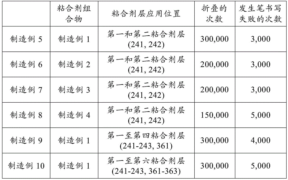
参考表2,当将根据制造例1的紫外可固化粘合剂层应用于第一粘合剂层241和第二粘合剂层242时,在其中第一粘合剂层241和第二粘合剂层242中的每一个在25℃下具有0.09MPa的储能模量的制造例5中,折叠的次数是300,000,并且发生笔书写失败的次数是3,000。Referring to Table 2, when the UV-curable adhesive layer according to Production Example 1 was applied to the first
当将根据制造例2或制造例3的紫外可固化粘合剂层应用于第一粘合剂层241和第二粘合剂层242时,在其中第一粘合剂层241和第二粘合剂层242中的每一个在25℃下具有0.14MPa的储能模量(大于0.09MPa)的制造例6和其中第一粘合剂层241和第二粘合剂层242中的每一个在25℃下具有0.11MPa的储能模量(大于0.09MPa)的制造例7中,折叠的次数是200,000,并且发生笔书写失败的次数是3,000。When the UV-curable adhesive layer according to Production Example 2 or Production Example 3 is applied to the first
当将根据制造例4的紫外可固化粘合剂层应用于第一粘合剂层241和第二粘合剂层242时,在其中第一粘合剂层241和第二粘合剂层242中的每一个在25℃下具有0.20MPa的储能模量(大于0.14MPa)的制造例8中,折叠的次数是150,000,并且发生笔书写失败的次数是5,000。When the UV-curable adhesive layer according to Production Example 4 was applied to the first
此外,当将根据制造例1的紫外可固化粘合剂层应用于第一至第四粘合剂层241、242、243和361时,在其中第一至第四粘合剂层241、242、243、361中的每一个在25℃下具有0.09MPa的储能模量的制造例9中,发生笔书写失败的次数是4,000。当将根据制造例1的紫外光可固化粘合剂层应用于第一至第六粘合剂层241至243和361至363时,在其中第一至第六粘合剂层241至243和361至363中的每一个在25℃下具有0.09MPa的储能模量的制造例10中,折叠的次数是300,000,并且发生笔书写失败的次数是5,000。Further, when the UV-curable adhesive layer according to Production Example 1 was applied to the first to fourth
尽管本文已经描述了某些实施方案和实施方式,但其它实施方案和修改从本说明书中将是显而易见的。因此,本发明构思不限于此类实施方案,而是限于所附权利要求以及对本领域普通技术人员会显而易见的各种明显的修改和等同布置的较宽范围。While certain embodiments and implementations have been described herein, other embodiments and modifications will be apparent from this specification. Therefore, the inventive concept is not limited to such embodiments, but is limited to the appended claims and their broader scope with various obvious modifications and equivalent arrangements apparent to those skilled in the art.
Claims (20)
Applications Claiming Priority (2)
| Application Number | Priority Date | Filing Date | Title |
|---|---|---|---|
| KR10-2021-0042137 | 2021-03-31 | ||
| KR1020210042137A KR20220136584A (en) | 2021-03-31 | 2021-03-31 | Electronic products and display device |
Publications (1)
| Publication Number | Publication Date |
|---|---|
| CN115148093A true CN115148093A (en) | 2022-10-04 |
Family
ID=83405242
Family Applications (1)
| Application Number | Title | Priority Date | Filing Date |
|---|---|---|---|
| CN202210250815.XA Pending CN115148093A (en) | 2021-03-31 | 2022-03-15 | Electronic product and display device |
Country Status (3)
| Country | Link |
|---|---|
| US (1) | US11726629B2 (en) |
| KR (1) | KR20220136584A (en) |
| CN (1) | CN115148093A (en) |
Families Citing this family (3)
| Publication number | Priority date | Publication date | Assignee | Title |
|---|---|---|---|---|
| KR20220025969A (en) * | 2020-08-24 | 2022-03-04 | 삼성디스플레이 주식회사 | Foldable window and display device comprisiing the foldable window |
| KR20240098191A (en) * | 2022-12-20 | 2024-06-28 | 삼성디스플레이 주식회사 | Electronic device |
| CN116246528A (en) * | 2023-01-10 | 2023-06-09 | 京东方科技集团股份有限公司 | Display module, manufacturing method thereof, and display device |
Family Cites Families (7)
| Publication number | Priority date | Publication date | Assignee | Title |
|---|---|---|---|---|
| CN101506969B (en) * | 2006-08-22 | 2011-08-31 | 三菱化学株式会社 | Member for semiconductor device, liquid for forming member for semiconductor device, method for producing member for semiconductor device, liquid for forming member for semiconductor device, phosphor composition, semiconductor light-emitting device, lighting device, and image display device manufactured by the method |
| PT2657301E (en) | 2010-12-22 | 2015-03-25 | Momentive Performance Mat Jp | Ultraviolet-curable silicone resin composition and image display device using same |
| JP6416687B2 (en) * | 2015-04-17 | 2018-10-31 | 株式会社ジャパンディスプレイ | Display device and touch detection device |
| KR102494986B1 (en) | 2016-01-11 | 2023-02-03 | 삼성디스플레이 주식회사 | Foldable display device |
| KR102489110B1 (en) | 2016-02-04 | 2023-01-16 | 삼성디스플레이 주식회사 | Display device |
| KR102024253B1 (en) | 2016-09-09 | 2019-09-23 | 주식회사 엘지화학 | Pressure Sensitive Adhesive composition using foldable display |
| KR102505265B1 (en) * | 2017-06-23 | 2023-03-06 | 삼성디스플레이 주식회사 | Electronic apparatus |
-
2021
- 2021-03-31 KR KR1020210042137A patent/KR20220136584A/en active Pending
-
2022
- 2022-01-13 US US17/575,531 patent/US11726629B2/en active Active
- 2022-03-15 CN CN202210250815.XA patent/CN115148093A/en active Pending
Also Published As
| Publication number | Publication date |
|---|---|
| KR20220136584A (en) | 2022-10-11 |
| US20220317791A1 (en) | 2022-10-06 |
| US11726629B2 (en) | 2023-08-15 |
Similar Documents
| Publication | Publication Date | Title |
|---|---|---|
| US11329250B2 (en) | Display device | |
| TWI716402B (en) | Flexible window substrate and flexible display device having the same | |
| CN113516911B (en) | Display device | |
| EP3238203B1 (en) | Window cover and display apparatus having the same and method of manufacturing display apparatus | |
| CN115148093A (en) | Electronic product and display device | |
| JP6244182B2 (en) | Transparent laminated film | |
| TWI767086B (en) | Circularly polarizing plate and display device | |
| CN109584720A (en) | Polarization plates and flexible display apparatus including it | |
| CN105843434A (en) | Flexible display device having flexible window substrate | |
| US11581499B2 (en) | Display device and method of manufacturing the same | |
| US11805669B2 (en) | Display device | |
| TW201923397A (en) | Circular polarizing plate and display device | |
| CN107039489A (en) | Display device | |
| EP3866218B1 (en) | Display device | |
| US20170054105A1 (en) | Bendable device with a window top layer | |
| CN112310304B (en) | Flexible display device | |
| US20240228842A1 (en) | Adhesive composition and display device | |
| CN220393597U (en) | Protective film, display module assembly and electronic equipment | |
| EP2405319A1 (en) | Monitor protection device for a flat panel display |
Legal Events
| Date | Code | Title | Description |
|---|---|---|---|
| PB01 | Publication | ||
| PB01 | Publication | ||
| SE01 | Entry into force of request for substantive examination | ||
| SE01 | Entry into force of request for substantive examination |