CN115136285A - Method of etching or deposition - Google Patents
Method of etching or deposition Download PDFInfo
- Publication number
- CN115136285A CN115136285A CN202180014408.2A CN202180014408A CN115136285A CN 115136285 A CN115136285 A CN 115136285A CN 202180014408 A CN202180014408 A CN 202180014408A CN 115136285 A CN115136285 A CN 115136285A
- Authority
- CN
- China
- Prior art keywords
- substrate
- precursor
- wocl
- reaction zone
- tungsten
- Prior art date
- Legal status (The legal status is an assumption and is not a legal conclusion. Google has not performed a legal analysis and makes no representation as to the accuracy of the status listed.)
- Pending
Links
Images


Classifications
-
- C—CHEMISTRY; METALLURGY
- C23—COATING METALLIC MATERIAL; COATING MATERIAL WITH METALLIC MATERIAL; CHEMICAL SURFACE TREATMENT; DIFFUSION TREATMENT OF METALLIC MATERIAL; COATING BY VACUUM EVAPORATION, BY SPUTTERING, BY ION IMPLANTATION OR BY CHEMICAL VAPOUR DEPOSITION, IN GENERAL; INHIBITING CORROSION OF METALLIC MATERIAL OR INCRUSTATION IN GENERAL
- C23C—COATING METALLIC MATERIAL; COATING MATERIAL WITH METALLIC MATERIAL; SURFACE TREATMENT OF METALLIC MATERIAL BY DIFFUSION INTO THE SURFACE, BY CHEMICAL CONVERSION OR SUBSTITUTION; COATING BY VACUUM EVAPORATION, BY SPUTTERING, BY ION IMPLANTATION OR BY CHEMICAL VAPOUR DEPOSITION, IN GENERAL
- C23C16/00—Chemical coating by decomposition of gaseous compounds, without leaving reaction products of surface material in the coating, i.e. chemical vapour deposition [CVD] processes
- C23C16/06—Chemical coating by decomposition of gaseous compounds, without leaving reaction products of surface material in the coating, i.e. chemical vapour deposition [CVD] processes characterised by the deposition of metallic material
- C23C16/08—Chemical coating by decomposition of gaseous compounds, without leaving reaction products of surface material in the coating, i.e. chemical vapour deposition [CVD] processes characterised by the deposition of metallic material from metal halides
-
- C—CHEMISTRY; METALLURGY
- C23—COATING METALLIC MATERIAL; COATING MATERIAL WITH METALLIC MATERIAL; CHEMICAL SURFACE TREATMENT; DIFFUSION TREATMENT OF METALLIC MATERIAL; COATING BY VACUUM EVAPORATION, BY SPUTTERING, BY ION IMPLANTATION OR BY CHEMICAL VAPOUR DEPOSITION, IN GENERAL; INHIBITING CORROSION OF METALLIC MATERIAL OR INCRUSTATION IN GENERAL
- C23C—COATING METALLIC MATERIAL; COATING MATERIAL WITH METALLIC MATERIAL; SURFACE TREATMENT OF METALLIC MATERIAL BY DIFFUSION INTO THE SURFACE, BY CHEMICAL CONVERSION OR SUBSTITUTION; COATING BY VACUUM EVAPORATION, BY SPUTTERING, BY ION IMPLANTATION OR BY CHEMICAL VAPOUR DEPOSITION, IN GENERAL
- C23C16/00—Chemical coating by decomposition of gaseous compounds, without leaving reaction products of surface material in the coating, i.e. chemical vapour deposition [CVD] processes
- C23C16/02—Pretreatment of the material to be coated
- C23C16/0227—Pretreatment of the material to be coated by cleaning or etching
- C23C16/0236—Pretreatment of the material to be coated by cleaning or etching by etching with a reactive gas
-
- C—CHEMISTRY; METALLURGY
- C23—COATING METALLIC MATERIAL; COATING MATERIAL WITH METALLIC MATERIAL; CHEMICAL SURFACE TREATMENT; DIFFUSION TREATMENT OF METALLIC MATERIAL; COATING BY VACUUM EVAPORATION, BY SPUTTERING, BY ION IMPLANTATION OR BY CHEMICAL VAPOUR DEPOSITION, IN GENERAL; INHIBITING CORROSION OF METALLIC MATERIAL OR INCRUSTATION IN GENERAL
- C23C—COATING METALLIC MATERIAL; COATING MATERIAL WITH METALLIC MATERIAL; SURFACE TREATMENT OF METALLIC MATERIAL BY DIFFUSION INTO THE SURFACE, BY CHEMICAL CONVERSION OR SUBSTITUTION; COATING BY VACUUM EVAPORATION, BY SPUTTERING, BY ION IMPLANTATION OR BY CHEMICAL VAPOUR DEPOSITION, IN GENERAL
- C23C16/00—Chemical coating by decomposition of gaseous compounds, without leaving reaction products of surface material in the coating, i.e. chemical vapour deposition [CVD] processes
- C23C16/04—Coating on selected surface areas, e.g. using masks
-
- C—CHEMISTRY; METALLURGY
- C23—COATING METALLIC MATERIAL; COATING MATERIAL WITH METALLIC MATERIAL; CHEMICAL SURFACE TREATMENT; DIFFUSION TREATMENT OF METALLIC MATERIAL; COATING BY VACUUM EVAPORATION, BY SPUTTERING, BY ION IMPLANTATION OR BY CHEMICAL VAPOUR DEPOSITION, IN GENERAL; INHIBITING CORROSION OF METALLIC MATERIAL OR INCRUSTATION IN GENERAL
- C23C—COATING METALLIC MATERIAL; COATING MATERIAL WITH METALLIC MATERIAL; SURFACE TREATMENT OF METALLIC MATERIAL BY DIFFUSION INTO THE SURFACE, BY CHEMICAL CONVERSION OR SUBSTITUTION; COATING BY VACUUM EVAPORATION, BY SPUTTERING, BY ION IMPLANTATION OR BY CHEMICAL VAPOUR DEPOSITION, IN GENERAL
- C23C16/00—Chemical coating by decomposition of gaseous compounds, without leaving reaction products of surface material in the coating, i.e. chemical vapour deposition [CVD] processes
- C23C16/06—Chemical coating by decomposition of gaseous compounds, without leaving reaction products of surface material in the coating, i.e. chemical vapour deposition [CVD] processes characterised by the deposition of metallic material
- C23C16/08—Chemical coating by decomposition of gaseous compounds, without leaving reaction products of surface material in the coating, i.e. chemical vapour deposition [CVD] processes characterised by the deposition of metallic material from metal halides
- C23C16/14—Deposition of only one other metal element
-
- C—CHEMISTRY; METALLURGY
- C23—COATING METALLIC MATERIAL; COATING MATERIAL WITH METALLIC MATERIAL; CHEMICAL SURFACE TREATMENT; DIFFUSION TREATMENT OF METALLIC MATERIAL; COATING BY VACUUM EVAPORATION, BY SPUTTERING, BY ION IMPLANTATION OR BY CHEMICAL VAPOUR DEPOSITION, IN GENERAL; INHIBITING CORROSION OF METALLIC MATERIAL OR INCRUSTATION IN GENERAL
- C23C—COATING METALLIC MATERIAL; COATING MATERIAL WITH METALLIC MATERIAL; SURFACE TREATMENT OF METALLIC MATERIAL BY DIFFUSION INTO THE SURFACE, BY CHEMICAL CONVERSION OR SUBSTITUTION; COATING BY VACUUM EVAPORATION, BY SPUTTERING, BY ION IMPLANTATION OR BY CHEMICAL VAPOUR DEPOSITION, IN GENERAL
- C23C16/00—Chemical coating by decomposition of gaseous compounds, without leaving reaction products of surface material in the coating, i.e. chemical vapour deposition [CVD] processes
- C23C16/44—Chemical coating by decomposition of gaseous compounds, without leaving reaction products of surface material in the coating, i.e. chemical vapour deposition [CVD] processes characterised by the method of coating
- C23C16/4401—Means for minimising impurities, e.g. dust, moisture or residual gas, in the reaction chamber
- C23C16/4408—Means for minimising impurities, e.g. dust, moisture or residual gas, in the reaction chamber by purging residual gases from the reaction chamber or gas lines
-
- C—CHEMISTRY; METALLURGY
- C23—COATING METALLIC MATERIAL; COATING MATERIAL WITH METALLIC MATERIAL; CHEMICAL SURFACE TREATMENT; DIFFUSION TREATMENT OF METALLIC MATERIAL; COATING BY VACUUM EVAPORATION, BY SPUTTERING, BY ION IMPLANTATION OR BY CHEMICAL VAPOUR DEPOSITION, IN GENERAL; INHIBITING CORROSION OF METALLIC MATERIAL OR INCRUSTATION IN GENERAL
- C23C—COATING METALLIC MATERIAL; COATING MATERIAL WITH METALLIC MATERIAL; SURFACE TREATMENT OF METALLIC MATERIAL BY DIFFUSION INTO THE SURFACE, BY CHEMICAL CONVERSION OR SUBSTITUTION; COATING BY VACUUM EVAPORATION, BY SPUTTERING, BY ION IMPLANTATION OR BY CHEMICAL VAPOUR DEPOSITION, IN GENERAL
- C23C16/00—Chemical coating by decomposition of gaseous compounds, without leaving reaction products of surface material in the coating, i.e. chemical vapour deposition [CVD] processes
- C23C16/44—Chemical coating by decomposition of gaseous compounds, without leaving reaction products of surface material in the coating, i.e. chemical vapour deposition [CVD] processes characterised by the method of coating
- C23C16/455—Chemical coating by decomposition of gaseous compounds, without leaving reaction products of surface material in the coating, i.e. chemical vapour deposition [CVD] processes characterised by the method of coating characterised by the method used for introducing gases into reaction chamber or for modifying gas flows in reaction chamber
- C23C16/45523—Pulsed gas flow or change of composition over time
- C23C16/45525—Atomic layer deposition [ALD]
- C23C16/45527—Atomic layer deposition [ALD] characterized by the ALD cycle, e.g. different flows or temperatures during half-reactions, unusual pulsing sequence, use of precursor mixtures or auxiliary reactants or activations
-
- C—CHEMISTRY; METALLURGY
- C23—COATING METALLIC MATERIAL; COATING MATERIAL WITH METALLIC MATERIAL; CHEMICAL SURFACE TREATMENT; DIFFUSION TREATMENT OF METALLIC MATERIAL; COATING BY VACUUM EVAPORATION, BY SPUTTERING, BY ION IMPLANTATION OR BY CHEMICAL VAPOUR DEPOSITION, IN GENERAL; INHIBITING CORROSION OF METALLIC MATERIAL OR INCRUSTATION IN GENERAL
- C23C—COATING METALLIC MATERIAL; COATING MATERIAL WITH METALLIC MATERIAL; SURFACE TREATMENT OF METALLIC MATERIAL BY DIFFUSION INTO THE SURFACE, BY CHEMICAL CONVERSION OR SUBSTITUTION; COATING BY VACUUM EVAPORATION, BY SPUTTERING, BY ION IMPLANTATION OR BY CHEMICAL VAPOUR DEPOSITION, IN GENERAL
- C23C16/00—Chemical coating by decomposition of gaseous compounds, without leaving reaction products of surface material in the coating, i.e. chemical vapour deposition [CVD] processes
- C23C16/44—Chemical coating by decomposition of gaseous compounds, without leaving reaction products of surface material in the coating, i.e. chemical vapour deposition [CVD] processes characterised by the method of coating
- C23C16/455—Chemical coating by decomposition of gaseous compounds, without leaving reaction products of surface material in the coating, i.e. chemical vapour deposition [CVD] processes characterised by the method of coating characterised by the method used for introducing gases into reaction chamber or for modifying gas flows in reaction chamber
- C23C16/45523—Pulsed gas flow or change of composition over time
- C23C16/45525—Atomic layer deposition [ALD]
- C23C16/45553—Atomic layer deposition [ALD] characterized by the use of precursors specially adapted for ALD
-
- H10P14/412—
-
- H10P14/43—
-
- H10P50/266—
-
- H10P50/285—
Landscapes
- Chemical & Material Sciences (AREA)
- Engineering & Computer Science (AREA)
- General Chemical & Material Sciences (AREA)
- Chemical Kinetics & Catalysis (AREA)
- Materials Engineering (AREA)
- Mechanical Engineering (AREA)
- Metallurgy (AREA)
- Organic Chemistry (AREA)
- Electrodes Of Semiconductors (AREA)
- Chemical Vapour Deposition (AREA)
- Manufacturing & Machinery (AREA)
- Physics & Mathematics (AREA)
- Condensed Matter Physics & Semiconductors (AREA)
- General Physics & Mathematics (AREA)
- Computer Hardware Design (AREA)
- Microelectronics & Electronic Packaging (AREA)
- Power Engineering (AREA)
- Drying Of Semiconductors (AREA)
- Internal Circuitry In Semiconductor Integrated Circuit Devices (AREA)
- Inorganic Chemistry (AREA)
- Crystals, And After-Treatments Of Crystals (AREA)
- Weting (AREA)
Abstract
本发明提供一种方法,用于(a)蚀刻Al2O3、HfO2、ZrO2、W、Mo、Co、Ru、SiN或TiN的膜,或(b)将钨沉积于选自Al2O3、HfO2、ZrO2、W、Mo、Co、Ru、Ir、SiN、TiN、TaN、WN及SiO2的膜的表面上,或(c)将钨选择性沉积于金属衬底(例如W、Mo、Co、Ru、Ir及Cu)上,而非沉积于金属氮化物或介电氧化物膜上,所述方法包括在工艺条件下在还原气体存在下使所述膜暴露于WOCl4。

The present invention provides a method for (a) etching a film of Al 2 O 3 , HfO 2 , ZrO 2 , W, Mo, Co, Ru, SiN or TiN, or (b) depositing tungsten on a film selected from Al 2 on the surface of films of O3 , HfO2 , ZrO2, W, Mo, Co, Ru, Ir, SiN, TiN, TaN, WN, and SiO2 , or (c) selective deposition of tungsten on metal substrates such as W, Mo, Co, Ru, Ir, and Cu), rather than on metal nitride or dielectric oxide films, the method comprising exposing the film to WOCl in the presence of a reducing gas under process conditions .
Description
Technical Field
The present disclosure generally relates to etching certain materials (including aluminum oxide, zirconium oxide, hafnium oxide, and combinations thereof, as well as titanium nitride, tantalum nitride, tungsten nitride) and using WOCl 4 Tungsten is deposited on certain materials, including tungsten, molybdenum, cobalt, ruthenium, aluminum oxide, titanium nitride, tantalum nitride, tungsten nitride, and silicon dioxide films present on microelectronic devices.
Background
On many microelectronic devices, particularly with atomic layer etching, aluminum oxide (Al) appears as a capacitor film 2 O 3 ) Etching of surfaces represents a great interest. Current methods typically require multiple steps, are complex and expensive. In addition, nucleation of the metal and generally a high level of deposition on the surface of the aluminum oxide film have proven difficult, and even if successful, adhesion between these two materials has not been satisfactory. Furthermore, existing methods generally fail to provide conformal coverage of tungsten on the alumina surface. For contact, interconnect, nucleation layer, seed layer applications and for hard mask applications, it may be desirable to deposit tungsten metal onto a variety of substrates. With respect to all of these possible applications, a high purity metal with uniformity within the deposited film is desirable to achieve the highest performance levels of the deposited film.
Disclosure of Invention
In general, the present disclosure provides a method for (a) etching Al 2 O 3 、HfO 2 、ZrO 2 W, Mo, Co, Ru, SiN or TiN, or (b) depositing tungsten on a layer selected from Al 2 O 3 、HfO 2 、ZrO 2 W, Mo, Co, Ru, Ir, SiN, TiN, TaN, WN and SiO 2 On the surface of a film of (2), saidThe method includes exposing the membrane to WOCl in the presence of a reducing gas under heterogeneous process conditions 4 Wherein the film is etched or tungsten is deposited on the surface of the film. The variation between the main etch process or main deposition process can be controlled by the following method: 1) changing the temperature of the substrate (i.e., (T) sub ) ); 2) direct change of WOCl via manipulation of precursor vapor pressure, deposition (or etch) pressure, or concentration 4 Gas phase concentration of the precursor; and/or 3) altering exposure to WOCl 4 The type of substrate that is vaporized.
Accordingly, in one aspect, the present disclosure provides a method comprising:
exposing a substrate to WOCl in a reaction zone under the following conditions 4 And a reducing gas:
(a) controllably etching a substrate under a first set of heterogeneous process conditions, wherein the substrate comprises Al selected from 2 O 3 、TiN、HfO 2 、ZrO 2 W, Mo, Co, Ru, and SiN films; or
(b) Controllably depositing tungsten on a surface of a substrate under a second set of heterogeneous process conditions, wherein the substrate comprises a material selected from Al 2 O 3 、HfO 2 、ZrO 2 W, Mo, Co, Ru, SiN, TiN, and SiO 2 A film of the film.
In another aspect, the present disclosure provides a method comprising:
in the reaction zone, the catalyst comprises Al 2 O 3 、TiN、HfO 2 、ZrO 2 Substrates of films of W, Mo, Co, Ru and SiN films were exposed to (i) WOCl 4 Along with a carrier gas delivered from a precursor ampoule, and (ii) a reducing gas, wherein the pressure in the reaction zone is about 0.5 to 500 torr; the substrate temperature is about 200 ℃ to 1000 ℃, the reducing gas flow rate is about 0.1 to 10 liters per minute, the carrier gas flow rate is about 0.001 to 1 liter per minute, WOCl 4 The concentration in the reaction zone is greater than 1000ppm, and the precursor ampoule temperature is from about 10 ℃ to about 180 ℃, whereby the etch comprises a metal selected from Al 2 O 3 、TiN、HfO 2 、ZrO 2 And films of W, Mo, Co, Ru and SiN films.
In another aspect, the present disclosure provides a method comprising:
in the reaction zone, the catalyst comprises Al 2 O 3 、HfO 2 、ZrO 2 W, Mo, Co, Ru, SiN, TiN, and SiO 2 Exposing a substrate of a film of the film to (i) WOCl 4 Along with a carrier gas delivered from a precursor ampoule, and (ii) a reducing gas, wherein the pressure in the reaction zone is about 0.5 torr to 500 torr; the substrate temperature is about 200 ℃ to 1000 ℃, the reducing gas flow rate is about 0.1 to 10 liters per minute, the carrier gas flow rate is about 0.001 to 1 liter per minute, WOCl 4 Is less than 1000ppm, and the precursor ampoule temperature is from about 10 ℃ to about 180 ℃, thereby depositing tungsten on the substrate comprising a metal selected from the group consisting of Al 2 O 3 、HfO 2 、ZrO 2 W, Mo, Co, Ru, SiN, TiN and SiO 2 On the surface of the substrate of the membrane.
In another aspect, the present disclosure provides a method comprising:
in the reaction zone, the catalyst comprises Al 2 O 3 、HfO 2 、ZrO 2 W, Mo, Co, Ru, Cu, Ir, SiN, TiN and SiO 2 Exposing a substrate of a film of the film to (i) WOCl 4 Along with a carrier gas delivered from a precursor ampoule, and (ii) a co-reactant reduction gas, wherein the pressure in the reaction zone is about 0.5 torr to 500 torr; the substrate temperature is about 200 ℃ to 1000 ℃, the reducing gas flow rate is about 0.1 to 10 liters per minute, the carrier gas flow rate is about 0.001 to 1 liter per minute, WOCl 4 Is less than 1000ppm, and the precursor ampoule temperature is between about 10 c and about 180 c, thereby selectively depositing tungsten on the metal conductor film (e.g., W, Mo, Co, Ru, Cu, Ir), and other suitable metal conductor films, rather than on the nitride and/or dielectric oxide film.
Drawings
The disclosure may be more completely understood in consideration of the following description of various illustrative embodiments in connection with the accompanying drawings.
FIG. 1 shows Al in a Chemical Vapor Etching (CVE) process 2 O 3 Etch rate Graph against substrate temperature (deg.C).
Fig. 2 is a graph of the etch rate of TiN at temperatures of 430, 475, and 520 ℃. Plotting TiN etch rates in a pulsed chemical vapor etch (pulsed CVE) process Graph against cycle number.
FIG. 3 is a graph showing the use of WOCl 4 As a graph of tungsten deposition on TiN at temperatures of 430, 475 and 520 ℃. This data was obtained using 80 Torr pressure, 100sccm argon carrier gas, and 2000sccm H 2 Pulsed chemical vapor deposition conditions of flow rate are generated. Is drawn with Tungsten deposition in units versus cycle number.
FIG. 4 illustrates the use of WOCl 4 As a precursor, pulsed chemical vapor deposition (pulsed CVD) of tungsten on titanium nitride. Is drawn with Graph of tungsten deposition in units and pulse "on time" in seconds for the precursor.
FIG. 5 illustrates the use of WOCl 4 As a precursor, the effect of the pulse "off time" on the exposure of the titanium nitride substrate to pulsed CVD conditions. Other conditions include a pressure of 80 Torr, 100sccm of argon carrier gas and 1000sccm of continuous H 2 And (4) flow rate. The titanium nitride etch rate is plotted against the pulse "off time".
Fig. 6 is a simplified depiction of an Atomic Layer Deposition (ALD) process practicing the methods of the present disclosure.
Fig. 7 is a simplified depiction of a Chemical Vapor Deposition (CVD) process practicing the methods of the present disclosure.
Fig. 8 is a simplified depiction of a "pulsed CVD" process practicing the methods of the present disclosure.
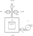
Figure 9 is a simplified depiction of a reaction chamber suitable for carrying out the methods of the present disclosure.
While the disclosure is amenable to various modifications and alternative forms, specifics thereof have been shown by way of example in the drawings and will be described in detail. However, it should be understood that the disclosure is not limited to the particular illustrative embodiments described herein. On the contrary, the intention is to cover all modifications, equivalents, and alternatives falling within the spirit and scope of the disclosure.
Detailed Description
As used in this specification and the appended claims, the singular forms "a", "an", and "the" include plural referents unless the context clearly dictates otherwise. As used in this specification and the appended claims, the term "or" is generally employed in its sense including "and/or" unless the context clearly dictates otherwise.
The term "about" generally refers to a range of numbers that are considered equivalent to the recited value (e.g., having the same function or result). In many instances, the term "about" may include numerical values that are rounded to the nearest significant figure.
The use of endpoints to indicate a range of values includes all values within that range (e.g., 1 to 5 includes 1, 1.5, 2, 2.75, 3, 3.80, 4, and 5).
As indicated above, in a first aspect, the present disclosure provides a method comprising:
exposing a substrate to WOCl in a reaction zone under the following conditions 4 And a reducing gas:
(a) controllably etching a substrate containing Al under a first set of process conditions 2 O 3 Or a substrate film of TiN; or
(b) Controllably depositing tungsten on a surface of a substrate under a second set of process conditions, wherein the substrate is selected from Al 2 O 3 、HfO 2 、ZrO 2 W, Mo, Co, Ru, SiN, TiN, and SiO 2 And (3) a membrane.
In general, the process conditions referenced above are those shared by chemical vapor deposition and atomic layer deposition. In this regard, the pressure is generally from about 1 torr to about 80 torr, and the temperature is from about 350 ℃ to about 750 ℃. Adding WOCl 4 Precursor materials and desired substratesAnd an inert carrier gas (e.g., argon, helium, or nitrogen) is fed into the reaction chamber along with a co-reactant reducing gas (e.g., hydrogen). The co-reactant reducing gas is a gas introduced into the system that reacts with the precursor material to produce an intermediate compound and/or a reaction by-product. The film can be deposited or etched through the use of CVD, pulsed CVD and/or ALD reaction processes.
The co-reactant reducing gas can be selected from those known in the CVD/ALD art and include H 2 、NH 3 Hydrazine and alkylated hydrazines (e.g. N) 2 H 4 、CH 3 HNNH 2 、CH 3 HNNHCH 3 )。
In certain embodiments, the method is performed in a single phase and the substrate is processed under controlled conditions for a selected time period to etch or deposit tungsten on a selected film. In certain embodiments and process conditions, etching occurs first, followed by deposition.
In other embodiments, the reaction can be carried out in a pulsed process. In this process, sequential processing steps are generally referred to as "pulsing" or cycling. These processes are based on controlled, self-limiting surface reactions of precursor chemicals. Gas phase reactions are avoided by contacting the substrate with one or more precursors alternately and sequentially. The process reactants are separated from each other on the substrate surface in time, for example by removing excess reactants and/or reactant byproducts from the reaction chamber between reactant pulses. In some embodiments, the precursor is pulsed into the chamber while a co-reactant reducing gas is continuously flowed into the reactor. This embodiment will be referred to as a "pulsed CVD" mode. In some embodiments, one or more substrate surfaces are contacted with two or more process precursors or reactants alternately and sequentially. Contacting the substrate surface with a gas phase reactant means that the reactant vapor is in contact with the substrate surface for a limited or controllable period of time. In other words, the substrate surface may be understood to be exposed to process precursors for a limited period of time.
Reactors that may be used to grow thin films can be used with the deposition described herein. These include ALD reactors, and are equipped to provide precursors (e.g., WOCl) in a "pulsed" manner 4 ) And suitable equipment and components for the co-reactant (i.e., reducing gas). According to certain embodiments, the sparger in the reactor may also be used to provide a supply of WOCl 4 The precursor is uniformly delivered to the wafer. Examples of suitable reactors that can be used include commercially available equipment, and self-made reactors, and will be known to those skilled in the art of CVD, pulsed CVD, and/or ALD. An exemplary reactor is shown in fig. 9.
Briefly, a substrate containing the desired films listed above is heated, typically at a pressure of about 0.5 to 500 torr, to a suitable deposition or etch temperature in the range of 200 ℃ to 1000 ℃. In other embodiments, the temperature is about 350 ℃ to 700 ℃ or 400 ℃ to 600 ℃. The deposition or etch temperature is generally kept below WOCl 4 The thermal decomposition temperature of the precursor is high enough to avoid condensation of the reactants and to provide sufficient energy to initiate the desired surface reaction. The surface of the substrate is in contact with WOCl 4 The precursors are contacted. In certain embodiments, WOCl is provided to a reaction space containing the substrate 4 A pulse of the precursor. In other embodiments, the substrate is moved to contain WOCl 4 A reaction space of the precursor. The process conditions are generally selected so that no more than about a monolayer of WOCl is present 4 The precursor adsorbs in a self-limiting manner onto the substrate surface. The appropriate contact time can be readily determined by a skilled artisan based on the particular process conditions, substrate, and reactor configuration. Removing excess WOCl from the substrate surface 4 The precursors and reaction byproducts, if any, are removed, for example, by purging with an inert gas, purging with a reducing gas, or by removing the substrate in the presence of the first reactant.
Purging means removing process precursors and/or process byproducts from the substrate surface and the process chamber, such as by evacuating the chamber using a vacuum pump and/or by replacing the gas inside the reactor with an inert gas (e.g., argon, helium, or nitrogen), and/or by replacing the gas inside the reactor with a reducing gas (e.g., hydrogen). In certain embodiments, the purge time is about 0.05 to 120 seconds, between about 0.05 to 10 seconds, or between about 0.05 to 2 seconds. However, other purge times may be utilized as desired, such as where highly conformal step coverage over very high aspect ratio structures or other complex topography structures is encountered.
In some embodiments, the phases of each cycle are generally self-limiting. Excess reactant precursors are supplied in each stage to saturate the sensitive structure surface. Surface saturation ensures that the reactants occupy all available reactive sites (e.g., the target is constrained by physical size or "steric hindrance"), and thus ensures excellent step coverage. Typically, less than one molecular layer of material is deposited per cycle, however, in some embodiments, more than one molecular layer is deposited during each cycle.
Removing excess reactants may include evacuating some of the contents of the reaction space and/or purging the reaction space with helium, nitrogen, argon, or another inert gas. In some embodiments, purging may be performed with a reducing gas. In certain embodiments, purging may include shutting off the flow of the reactive gas while continuing to flow the inert carrier gas or the reducing gas to the reaction space. In another embodiment, the purging step may employ a vacuum step to remove excess reactants from the surface. In certain embodiments, WOCl is added to the mixture 4 The precursor is pulsed into the reaction chamber containing the substrate/film for a period of about 0.05 to about 20 seconds, and then the carrier gas and co-reactant reduction gas are continuously flowed into the reactor, albeit unpulsed, thus serving to purge excess precursor from the reaction chamber. In a respective embodiment, the precursor is pulsed into the reaction chamber, then purged, a reducing gas is pulsed into the reactor, and then purged, and this cycle is repeated to achieve a desired thickness of the deposited tungsten film or removed by etching a desired thickness of the exposed film.
In the process of the present disclosure, the precursor WOCl is subjected to the following conditions 4 The use of (a) is biased towards thin film tungsten deposition:
pressure >0.5 torr to 500 torr;
temperature >200 ℃ to 1000 ℃;
·H 2 flow rate ═>0.1 to 10 liters per minute;
a carrier gas flow rate > 0.001 to 1 liter per minute; and
the precursor ampoule temperature >10 ℃ to 180 ℃.
Deposition of tungsten on various substrates is directly dependent on WOCl 4 Concentration of precursor (which is denoted herein as [ WOCl ] 4 ]) Substrate characteristics, and substrate temperature. Generally, but not strictly speaking, less than 1000ppm WOCl is required in a CVD process as exemplified herein 4 Concentration to perform tungsten film growth.
Additionally or alternatively, according to the methods of the present disclosure, WOCl is performed under the following conditions 4 Substrate etch bias:
pressure >0.5 torr to 500 torr;
temperature >200 ℃ to 1000 ℃;
·H 2 flow rate ═>0.1 to 10 liters per minute;
carrier gas flow > 0.001 to 1 liter per minute; and
precursor ampoule temperature >10 ℃ to 180 ℃.
The etching of various substrates is directly dependent on the concentration of the precursor [ WOCl ] 4 ]Substrate characteristics, and substrate temperature. Generally, but not strictly speaking, [ WOCl ] in a continuous exposure mode (i.e., CVE ═ chemical vapor etch) process 4 ]Concentration of (2)>1000 ppm. The concentration of the precursor depends on [ WOCl ] 4 ]Substrate material, and substrate temperature.
Further, additionally or alternatively, according to the method of the present disclosure, tungsten is selectively deposited on the metal conductor film by including Al selected from the group consisting of Al in the reaction zone under the following conditions 2 O 3 、HfO 2 、ZrO 2 W, Mo, Co, Ru, Cu, Ir, SiN, TiN and SiO 2 Exposing a substrate of a film of the film to (i) WOCl 4 Along with a carrier gas delivered from the precursor ampoule, and (ii) a co-reactant reducing gas,
the pressure in the reaction zone is from about 0.5 torr to 500 torr;
the substrate temperature is about 200 to 1000 c,
the flow rate of the reducing gas is about 0.1 to 10 liters per minute,
the carrier gas flow rate is about 0.001 to 1 liter per minute,
·[WOCl 4 ]is less than 1000ppm, and
the precursor ampoule temperature is from about 10 c to about 180 c,
because of these process conditions, tungsten is thus selectively deposited on metal conductor films (e.g., W, Mo, Co, Ru, Cu, Ir) and other suitable metal conductor films, rather than on nitride and/or dielectric oxide films.
Examples of the invention
TABLE 1

In examples 1 to 5, the results are summarized in Table 1 above, measured before and after the use of X-ray fluorescence (XRF). The positive (+) number indicates tungsten film deposition, and the negative (-) number indicates substrate film etching. In these experiments, WOCl 4 The ampoule temperature was set at 90 deg.C, the Ar carrier gas flow rate was set at 100sccm (standard cubic centimeters per minute, i.e., flow rate), and WOCl was allowed to flow 4 Exposure to the substrate took about 600 seconds. As can be seen in the table, Al was used in this study due to the lack of competing tungsten deposition processes noted at higher temperatures 2 O 3 With the highest exposure etch rate per minute. In addition, it was observed that the etch rate was dependent on the precursor [ WOCl ] 4 ]Concentration, substrate characteristics and T sub (i.e., substrate temperature). Higher precursor concentrations and higher substrate temperatures result in substrate etching, while tungsten deposition is observed when the precursor concentration is too low to etch the substrate. Tungsten deposition was observed at 550 deg.C And 650 deg.C
 The substrate etch occurs at 400 deg.C
 The following occurs. In these tungsten deposition examples, the resistivity of the resulting films was found to be as low as 11.5 μ Ω -cm on tungsten substrates (example 3) and 26.7 μ Ω -cm on TiN substrates. In addition, it was shown that high precursor concentrations resulted in columnar crystal growth on tungsten substrates (i.e., isolated grains) and at higher Tds sub The lower has a higher resistivity (19 μ Ω -cm).
As can be pointed out by the data in table 1, tungsten metal is selectively deposited on tungsten or other suitable metal conductor films (e.g., Mo, Co, Ru, Ir, and Cu), rather than on nitride and/or dielectric oxide films, which can be achieved by careful control of process conditions during deposition. In some embodiments, a pre-etch of the substrate may be used prior to selective deposition to enhance contact resistance and thin film adhesion properties. Without wishing to be bound by theory, selective deposition of tungsten metal on other suitable metal conductor films (e.g., Mo, Co, Ru, Ir, and Cu), rather than on nitride and/or dielectric oxide films, can also be achieved by careful control of process conditions during deposition.
TABLE 2

In examples 6 to 10, the results are summarized in Table 2, the flow rate of the argon carrier gas is set to 100sccm, H 2 The flow rate of the gas was set at 2000sccm and the tungsten CVD deposition time was 600 seconds. From the data in Table 2, it can be observed that, under most of the test conditions, WOCl 4 The titanium nitride is etched. It can also be observed that at lower precursor concentrations, for higher T sub The rate/extent of the titanium nitride etch is increased, while the tungsten deposition occurs only at 650 ℃.
TABLE 3a (H only) 2 )


TABLE 3b (argon only)

In examples 11 to 20, the results are summarized in tables 3a and 3b, the argon loading used is 100 sccm; in Table 3a, H 2 The gas was introduced at a rate of 2000sccm (no other argon gas). In Table 3b, argon carrier gas (no other H) was added at a rate divided by 100sccm 2 Gas), argon purge gas was introduced at a rate of 2000 sccm. In general, Al 2 O 3 Lower etch rate in Ar than when H is used 2 A co-reactant gas stream. This data can also be displayed with H 2 At low substrate temperature conditions and low chamber pressure (higher WOCl) 4 Concentration) of Al, Al 2 O 3 Etching is faster in argon.
TABLE 4

Unknown
Examples 21 to 25 relate to etching SiO 2 An attempt to do so. The results are summarized in Table 4. In these experiments, the argon carrier gas used was 100sccm, and H was used 2 The gas was 2000 sccm. Tungsten deposition only occurs at lower precursor concentrations at 650 ℃. The resistivity is about 18 μ Ω -cm. At any temperature for [ WOCl ] 4 ]<1000ppm, SiO was not observed 2 And (6) etching. Without wishing to be bound by theory, based on the mechanics of the etching process, it is believed that in some instances, in WOCl 4 At higher concentration of precursor, SiO 2 The etching of (a) may occur slowly.
TABLE 5


In examples 26 through 34, the results of which are shown in Table 5 above, a titanium nitride substrate was subjected to pulsed CVD conditions using a precursor chamber pressure of 80 Torr, 100sccm of argon carrier gas, 2000sccm of H 2 Gas (continuous). WOCl 4 The pulses of the precursor were for 1 second in a 40 second cycle interval. The WOCl 4 The number of pulse cycles of the precursor was 1, 5, 10, 15 and 25 cycles, respectively. This data shows that the titanium nitride etch rate in the first cycle is significant in this pulsed CVD process, and that>The drop is sharp in 5 cycles. As the number of cycles increases to over 10 cycles, tungsten deposition begins to occur. In addition, the lower substrate temperature (430 ℃) increased the titanium nitride etch rate by about 10% in the first cycle.
TABLE 6

In experiments 35 to 37, the results are summarized in Table 6, and the data are obtained using pulsed chemical vapor deposition conditions with WOCl 4 As a precursor generation, the pulsed chemical vapor deposition conditions included a precursor chamber pressure of 80 Torr and an argon carrier gas rate of 100 sccm. In examples 35 to 37, H 2 The gas was injected into the reactor chamber at a constant rate of 2000 sccm. In examples 35 to 37, WOCl was increased for 10 seconds on time 4 The precursor "on-time" increases the titanium nitride etch rate by 30%. In addition, the tungsten deposition rate increased with increasing on-time for 15 cycles of operation. Note that: the loss increase of TiN may be due to loss of x-ray signal through the tungsten film.
TABLE 7

The examples in Table 7 show the use of 100sccm of argon carrier gas, 2000sccm of H under CVD conditions 2 (continuous), and tungsten deposition for 600, 300, and 300 seconds, respectively, the titanium nitride substrate is etched. This data illustrates that the precursor (WOCl) is increased 4 ) Concentration increase etch rate; the precursor concentration may be increased by decreasing the chamber pressure, decreasing the co-reactant reducing gas, and/or increasing the ampoule temperature.
TABLE 8a

TABLE 8b

In each of examples 42-47, the data is summarized in tables 8a and 8b, the precursor is WOCl 4 ,H 2 The gas flow rate was 2000sccm, the tungsten deposition time was 300s, the chamber pressure was 10 Torr, and the resulting tungsten thickness was The data in Table 8a shows that the titanium nitride etch rate does not follow T since the reaction is carried out at a pressure of 10 Torr in a mass transport limited regime sub And (4) changing. Table 8b shows that increasing the precursor carrier gas increases the precursor concentration and the titanium nitride etch rate, thus showing that the mass transport rate of the etch is limited to 430 ℃. In addition, the mass transport of titanium nitride etching is limited to a pressure of 10 torr and the surface reaction rate is limited to a pressure of 80 torr.
TABLE 9

In factIn each of examples 48 to 50 (ALE process), the data are summarized in Table 9, where the precursor is WOCl 4 Ar carrier gas flow rate of 200sccm, H 2 The gas flow rate was 2000sccm, the argon purge gas flow rate was 500sccm, the tungsten deposition time was 60 cycles, and the substrate temperature was 520 ℃. This data shows that the deposition rate of tungsten on titanium nitride decreases with decreasing pressure (from 80 torr to 20 torr) (i.e., WOCl) 4 The concentration increases). In addition, the TiN etch rate increases with decreasing pressure; however, 40 torr may indicate a transition between deposition and etching. Under these process conditions, the resistivity of the deposited tungsten film is very good. This data also describes that substrate etching and deposition can occur without changing experimental conditions, and can compete in real time.

In each of examples 51-52, the data is summarized in Table 10, with the precursor being WOCl 4 Argon carrier gas flow rate of 200sccm, H 2 The gas flow rate was 2000sccm, the argon purge gas flow rate was 500sccm, the tungsten deposition time was 60 cycles, the pressure was 20 torr, and the substrate temperature was 520 ℃. This data demonstrates an increase in WOCl 4 The "on time" increases both the tungsten deposition rate and the titanium nitride etch rate of the titanium nitride substrate. Tungsten resistivity shows little change under these process conditions.
TABLE 11

In examples 53 and 54, the data are summarized in Table 11, the precursor is WOCl 4 Ar carrier gas flow rate of 200sccm, H 2 The gas flow rate was 2000sccm, the argon purge gas flow rate was 500sccm, the pressure was 20 torr, and the substrate temperature was 520 ℃. This data shows that there is about 30 cycle nucleation delays to deposit a layer of tungsten on the titanium nitride. In addition, tungsten is used in the processAfter coating the surface, the deposition rate increases with increasing number of cycles. The etch rate decreases with time and also with increasing tungsten coverage of the surface. Good tungsten resistivity was observed for these tungsten films.
TABLE 12
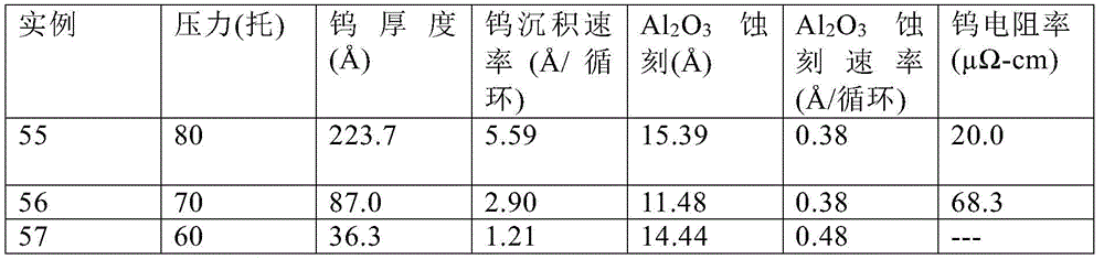
In each of examples 55 to 57, the data is summarized in Table 12 with the precursor being WOCl 4 Ar carrier gas flow rate of 200sccm, H 2 Gas flow rate of 1000sccm, argon purge gas flow rate of 500sccm, and Al 2 O 3 The substrate temperature was 650 ℃. Example 55 ran 40 cycles, and examples 56 and 57 ran 30 cycles. This data shows that the tungsten deposition rate decreases with decreasing pressure, while Al 2 O 3 The etch rate increases. As might be expected, the thinner the tungsten film, the higher the resistivity due to incomplete coverage and non-optimized morphology.
Watch 13

In each of examples 58-60, the data is summarized in Table 13 with the precursor being WOCl 4 ,H 2 Gas flow rate of 1000sccm, and Al 2 O 3 The substrate temperature was 650 ℃. This data shows tungsten deposition rate and Al 2 O 3 The etch rate decreases as the argon carrier gas flow decreases and the argon purge gas flow increases. The resistivity varies from about 23 to 59 μ Ω -cm.
TABLE 14

In each of examples 61-63, the data is summarized in Table 14, with the precursor being WOCl 4 Ar carrier gas flow rate of 50sccm, H 2 Gas flowA flow rate of 1000sccm, an argon purge gas flow rate of 700sccm, and Al 2 O 3 The substrate temperature was 650 ℃. This data shows that along with Al 2 O 3 The surface is covered with more and more tungsten, and the tungsten deposition rate increases with increasing number of cycles. Al (Al) 2 O 3 The etch rate is also increased, but it may be due to Al 2 O 3 The top tungsten film absorbs x-rays. As expected, the resistivity decreases with increasing tungsten film thickness due to the reduction of pinholes or voids in the tungsten film.
Adhesion test the results of ASTM D3359-02 show excellent adhesion, i.e., deposition on a titanium nitride substrate at 650 deg.C Film and deposition on alumina substrate
 The tungsten film is not peeled off from the substrate.
Referring to the figures and the experimental data listed above, FIG. 1 is Al 2 O 3 Etch rate Graph against substrate temperature (deg.C). This data shows that when compared to H, as compared to reaction with argon alone 2 During the co-reaction, Al 2 O 3 The etch rate is about twice. In addition, the etch rate decreases with decreasing pressure. Lower pressure increase WOCl 4 Which should increase the etching. This data indicates that deposition increases with increasing substrate temperature and thus reaction rates are limited, and residence time also determines etch rates. (see Table 1).
Fig. 2 is a graph of the etch rate of TiN at temperatures of 430, 475, and 520 ℃. Plotting TiN etch rates
 Graph against cycle number. See also tables 1 and 2 forThe data of (2). This data was generated using the following pulsed chemical vapor deposition conditions: 80 Torr pressure, 100sccm Ar carrier gas and 2000sccm of H as co-reactant 2 Flow, 1 second WOCl 4 Pulsed for a total cycle time of 40 seconds. The data for substrate temperatures of 430 and 475 ℃ illustrate operation in mass transfer rate limited processes because the etch rate does not increase with increasing substrate temperature. In addition, the amount of etching is limited, and the maximum portion of etching occurs in the first cycle and gradually decreases in the next 5 cycles.
FIG. 3 is a graph showing the use of WOCl 4 As a precursor, a graph of tungsten deposition on TiN at temperatures of 430, 475, and 520 ℃. This data was generated using the following pulsed chemical vapor deposition conditions: 80 Torr pressure, 100sccm of argon carrier gas and 2000sccm of H 2 And (4) flow rate. Mapping tungsten deposits Graph against cycle number. This data illustrates that tungsten deposition occurs after 5 cycles at 475 ℃ and 520 ℃ operating temperatures, but more time (after 10 cycles) is required for 430 ℃ operating temperatures, indicating that the substrate temperature is dependent on nucleation delay.
FIG. 4 illustrates the use of WOCl 4 As a precursor, tungsten was pulse CVD deposited on titanium nitride. Is drawn with Graph of tungsten deposition in relation to pulse "on time" in seconds for the precursor. This data illustrates that tungsten deposition increases significantly (-6 x) over a 10 second on-time of the precursor. Pulsed CVD conditions included 80 Torr pressure, 100sccm argon carrier gas, 2000sccm H 2 Flow rate (continuous). Under these conditions and at the substrate temperature (T) sub ) In the case of 430 ℃, tungsten deposition was not observed, but titanium nitride film etching was observed. (see Table 6)
FIG. 5 illustrates the use of WOCl 4 As a precursor, the effect of the pulse "off time" on the exposure of the titanium nitride substrate to the pulsed CVD conditions. Other conditions include a pressure of 80 Torr, 100sccm of argon carrier gas and a continuous flow of 1000sccmH 2 And (4) flow rate. The titanium nitride etch rate is plotted against the pulse "off time". As the shut-down time increases, the ampoule temperature increases and thus the precursor concentration increases as less Ar flow through the ampoule cools down. This figure also illustrates that the titanium nitride etch rate is directly dependent on WOCl 4 A precursor concentration; also in this case, there is no tungsten deposition because the exposure time is short (5 cycles).
Fig. 6 is a simplified depiction of an "ALD" (or "ALE" in the case of etching) process for practicing the methods of the present disclosure. WOCl 4 And the co-reactant (i.e., reducing gas) is pulsed "on" for a portion of the cycle time. A vacuum or inert gas purge occurs between the precursor and the co-reactant pulse. The cycle is repeated multiple times to produce a particular film thickness (or to achieve a desired amount of etching).
Fig. 7 is a simplified depiction of a "CVD" (or "CVE" in the case of etching) process for practicing the methods of the present disclosure. Adding WOCl 4 And the co-reactant are both continuously fed into the reaction zone until the desired amount of deposition (or etching) has occurred.
Fig. 8 is a simplified depiction of a "pulsed CVD" (or "CVE" in the case of etching) process for practicing the methods of the present disclosure. During a given period of time, WOCl is added 4 The precursor is injected into the reaction zone in a pulse followed by a "shut-down" period while the co-reactant is continuously fed into the reaction zone. In this way, when the pulse is "off, the co-reactant must purge the precursor from the reaction zone during these periods.
Fig. 9 is a simplified depiction of a reaction chamber suitable for carrying out the methods of the present disclosure.
Other aspects of the disclosure include the following:
aspect 1 is a method comprising exposing a substrate to WOCl in a reaction zone under conditions 4 And a reducing gas:
(a) controllably etching a substrate under a first set of process conditions, wherein the substrate comprises a material selected from Al 2 O 3 、TiN、HfO 2 、ZrO 2 、W、Mo、Co、Ru、Ir、Cu、SiO 2 And a film of SiN film;
(b) controllably depositing tungsten on a surface of a substrate under a second set of process conditions, wherein the substrate comprises a material selected from the group consisting of Al 2 O 3 、HfO 2 、ZrO 2 W, Mo, Co, Ru, Ir, Cu, SiN, TiN and SiO 2 A film of the film; or
(c) Under a third set of process conditions, tungsten is selectively deposited on the metallic conducting W, Mo, Co, Ru, Ir, Cu substrate, rather than on the adjacent nitride or dielectric oxide film.
Aspect 2 is the method of aspect 1, wherein the first set of process conditions comprises a substrate temperature range of about 200 ℃ to about 1000 ℃, a WOCl of about 800ppm to about 20,000ppm 4 Concentration, and a pressure of about 0.5 to about 500 torr.
Aspect 3 is the method of aspect 1, wherein the second set of process conditions comprises a substrate temperature range of about 200 ℃ to about 1000 ℃, a WOCl of about 5ppm to about 1200ppm 4 Concentration, and a pressure of about 0.5 to about 500 torr.
Aspect 4 is the method of aspect 1, wherein the reducing gas is selected from hydrogen, hydrazine or alkylated hydrazine.
Aspect 6 is a process comprising contacting in a reaction zone a catalyst comprising a metal selected from Al 2 O 3 、TiN、HfO 2 、ZrO 2 Substrates of films of W, Mo, Co, Ru and SiN films were exposed to (i) WOCl 4 Along with a carrier gas delivered from a precursor ampoule, and (ii) a reducing gas, wherein the pressure in the reaction zone is about 0.5 to 500 torr; the substrate temperature is about 200 ℃ to 1000 ℃, the reducing gas flow rate is about 0.1 to 10 liters per minute, the carrier gas flow rate is about 0.001 to 1 liter per minute, WOCl 4 The concentration in the reaction zone is greater than 1000ppm, and the precursor ampoule temperature is from about 10 ℃ to about 180 ℃, whereby the etch comprises a material selected from Al 2 O 3 、TiN、HfO 2 、ZrO 2 W, Mo, Co, Ru anda film of SiN film.
Aspect 7 is the method of aspect 6, wherein WOCl 4 The concentration in the reaction zone is from about 1000ppm to about 10,000 ppm.
Aspect 8 is the method of aspect 6, wherein the substrate is exposed to WOCl 4 Continuous flows of precursor and reducing gas.
Aspect 9 is the method of aspect 6, wherein the substrate is exposed to a continuous flow of reducing gas while the WOCl is simultaneously exposed to 4 A precursor pulse is introduced into the reaction zone for a predetermined time period.
Aspect 11 is the method of aspect 9, wherein the WOCl is added to the mixture 4 The precursor is pulsed into the reaction zone for a period of from.1 to about 10 seconds, followed by a shutdown period of from 1 to about 60.
Aspect 13 is the method of aspect 6, wherein the substrate is sequentially subjected to:
(i) exposure to WOCl 4 Precursor, then
(ii) By vacuum or inert gas purging, followed by
(iii) Is exposed to a reducing gas, followed by
(iv) (iii) purging by vacuum or inert gas and repeating the sequence of (i) to (iv) until the desired amount of etching has occurred on the substrate.
Aspect 16 is a process comprising contacting in a reaction zone a catalyst comprising a metal selected from the group consisting of Al 2 O 3 、HfO 2 、ZrO 2 W, Mo, Co, Ru, SiN, TiN and SiO 2 The substrate of the film is exposed to:
(i)WOCl 4 together with a carrier gas delivered from the precursor ampoule, and
(ii) the reduction gas is introduced into the reaction vessel,
wherein the pressure in the reaction zone is about 0.5 torr to 500 torr; the substrate temperature is about 200 ℃ to 1000 ℃, the reducing gas flow rate is about 0.1 to 10 liters per minute, the carrier gas flow rate is from about 0.001 to 1 liter per minute, the WOCl 4 Is less than 1000ppm, and the precursor ampoule temperature is from about 10 c to about 180 c,
thereby depositing tungsten on the substrate containing Al 2 O 3 、HfO 2 、ZrO 2 W, Mo, Co, Ru, SiN, TiN and SiO 2 On the surface of the substrate of the membrane.
Aspect 17 is the method of aspect 16, wherein WOCl 4 The concentration in the reaction zone is from about 75ppm to about 1000 ppm.
Aspect 18 is the method of aspect 16, wherein the substrate is sequentially subjected to:
(i) exposure to WOCl 4 Precursor, then
(ii) By vacuum or inert gas purging, followed by
(iii) Is exposed to a reducing gas, followed by
(iv) (iii) purging by vacuum or inert gas, and repeating the sequence of (i) to (iv) until the desired amount of tungsten has been deposited on the substrate.
Aspect 19 is the method of aspect 16, wherein the exposing is wherein the substrate is exposed to WOCl 4 Continuous flows of precursor and reducing gas.
Aspect 21 is the method of aspect 20, wherein WOCl is added 4 Pulsing a precursor into the reaction zone for a period of 0.1 to about 10 seconds followed by a shutdown period of 1 to about 60 seconds and repeating the desired amountThe pulse is pulsed until the desired amount of tungsten deposition has occurred on the substrate.
Aspect 22 is the method of aspect 16, wherein WOCl 4 The concentration of the precursor in the reaction zone is about 100ppm to about 800 ppm.
Aspect 23 is the method of aspect 16, wherein the substrate temperature is about 550 ℃ to about 700 ℃.
Aspect 24 is a method of selectively depositing tungsten on a metal conductor film comprising including in a reaction zone a metal selected from Al 2 O 3 、HfO 2 、ZrO 2 W, Mo, Co, Ru, Cu, Ir, SiN, TiN and SiO 2 Exposing a substrate of a film of the film to (i) WOCl 4 Along with a carrier gas delivered from the precursor ampoule, and (ii) a co-reactant reducing gas, under process conditions comprising: the pressure in the reaction zone is about 0.5 torr to 500 torr; the substrate temperature is about 200 ℃ to 1000 ℃; the reducing gas flow rate is about 0.1 to 10 liters per minute; a carrier gas flow rate of from about 0.001 to 1 liter per minute; [ WOCl ] 4 ]Wherein the precursor ampoule temperature is from about 10 ℃ to about 180 ℃, and
wherein tungsten is selectively deposited on metal conductor films (e.g., W, Mo, Co, Ru, Cu, Ir) and other suitable metal conductor films, rather than on nitride and/or dielectric oxide films.
Aspect 25 is a tungsten film having a thickness of about To about
 And each has a resistivity of about 100 to about 50 μ Ω -cm.
Aspect 26 is a tungsten film having an electrical conductivity of about To about
 And each has a resistivity of about 50 to about 13 μ Ω -cm.
Aspect 27 is a tungsten film having a thickness greater than And has a resistivity of less than about 15 μ Ω -cm.
Having thus described several illustrative embodiments of the disclosure, it will be apparent to one of ordinary skill in the art that yet other embodiments may be made and used within the scope of the following claims. Many advantages of the invention covered by this document have been enumerated in the foregoing description. It should be understood, however, that the present invention is, in many respects, only illustrative. Changes may be made in detail without departing from the scope of the invention. The scope of the invention is, of course, defined by the language in which the appended claims are expressed.
Claims (20)


Applications Claiming Priority (3)
| Application Number | Priority Date | Filing Date | Title |
|---|---|---|---|
| US202062961939P | 2020-01-16 | 2020-01-16 | |
| US62/961,939 | 2020-01-16 | ||
| PCT/US2021/013731 WO2021146623A1 (en) | 2020-01-16 | 2021-01-15 | Method for etching or deposition |
Publications (1)
| Publication Number | Publication Date |
|---|---|
| CN115136285A true CN115136285A (en) | 2022-09-30 |
Family
ID=76856731
Family Applications (1)
| Application Number | Title | Priority Date | Filing Date |
|---|---|---|---|
| CN202180014408.2A Pending CN115136285A (en) | 2020-01-16 | 2021-01-15 | Method of etching or deposition |
Country Status (7)
| Country | Link |
|---|---|
| US (1) | US11624111B2 (en) |
| EP (1) | EP4091192A4 (en) |
| JP (1) | JP7486588B2 (en) |
| KR (1) | KR102828205B1 (en) |
| CN (1) | CN115136285A (en) |
| TW (3) | TWI895106B (en) |
| WO (1) | WO2021146623A1 (en) |
Citations (5)
| Publication number | Priority date | Publication date | Assignee | Title |
|---|---|---|---|---|
| US8178439B2 (en) * | 2010-03-30 | 2012-05-15 | Tokyo Electron Limited | Surface cleaning and selective deposition of metal-containing cap layers for semiconductor devices |
| US20130196502A1 (en) * | 2011-12-09 | 2013-08-01 | ASM International. N.V. | Selective formation of metallic films on metallic surfaces |
| US20170062224A1 (en) * | 2015-08-28 | 2017-03-02 | Applied Materials, Inc. | Methods of Depositing Metal Films Using Metal Oxyhalide Precursors |
| US20180019165A1 (en) * | 2016-07-14 | 2018-01-18 | Entegris, Inc. | CVD Mo DEPOSITION BY USING MoOCl4 |
| US20190341268A1 (en) * | 2018-05-01 | 2019-11-07 | Applied Materials, Inc. | Methods Of Increasing Selectivity For Selective Etch Processes |
Family Cites Families (20)
| Publication number | Priority date | Publication date | Assignee | Title |
|---|---|---|---|---|
| JPH0923287A (en) * | 1995-07-07 | 1997-01-21 | Nippon Telegr & Teleph Corp <Ntt> | Monitoring information notification system using public telephone network |
| JPH09232287A (en) * | 1996-02-26 | 1997-09-05 | Sony Corp | Etching method and contact plug forming method |
| GB9816720D0 (en) * | 1998-08-01 | 1998-09-30 | Pilkington Plc | Process for coating glass |
| US20020176927A1 (en) * | 2001-03-29 | 2002-11-28 | Kodas Toivo T. | Combinatorial synthesis of material systems |
| US7579285B2 (en) * | 2005-07-11 | 2009-08-25 | Imec | Atomic layer deposition method for depositing a layer |
| JP6273257B2 (en) * | 2012-03-27 | 2018-01-31 | ノベラス・システムズ・インコーポレーテッドNovellus Systems Incorporated | Feature filling with tungsten |
| US20140273451A1 (en) * | 2013-03-13 | 2014-09-18 | Applied Materials, Inc. | Tungsten deposition sequence |
| US20150348840A1 (en) * | 2014-05-31 | 2015-12-03 | Lam Research Corporation | Methods of filling high aspect ratio features with fluorine free tungsten |
| TW201606115A (en) * | 2014-07-07 | 2016-02-16 | 液態空氣喬治斯克勞帝方法研究開發股份有限公司 | Molybdenum and tungsten precursors for thin film deposition |
| TWI656232B (en) * | 2014-08-14 | 2019-04-11 | 法商液態空氣喬治斯克勞帝方法研究開發股份有限公司 | Molybdenum compositions and their use to form molybdenum oxide films |
| US9972504B2 (en) * | 2015-08-07 | 2018-05-15 | Lam Research Corporation | Atomic layer etching of tungsten for enhanced tungsten deposition fill |
| CN109463005B (en) * | 2016-06-03 | 2023-12-15 | 恩特格里斯公司 | Vapor phase etching of hafnium dioxide and zirconium dioxide |
| US10014185B1 (en) * | 2017-03-01 | 2018-07-03 | Applied Materials, Inc. | Selective etch of metal nitride films |
| TWI719316B (en) * | 2017-06-12 | 2021-02-21 | 美商應用材料股份有限公司 | Seamless tungsten fill by tungsten oxidation-reduction |
| US10600688B2 (en) * | 2017-09-06 | 2020-03-24 | Micromaterials Llc | Methods of producing self-aligned vias |
| US10403504B2 (en) * | 2017-10-05 | 2019-09-03 | Asm Ip Holding B.V. | Method for selectively depositing a metallic film on a substrate |
| US10910262B2 (en) * | 2017-11-16 | 2021-02-02 | Asm Ip Holding B.V. | Method of selectively depositing a capping layer structure on a semiconductor device structure |
| KR102806630B1 (en) * | 2018-05-03 | 2025-05-12 | 램 리써치 코포레이션 | Method for depositing tungsten and other metals on 3D NAND structures |
| TW202203305A (en) * | 2018-05-04 | 2022-01-16 | 美商應用材料股份有限公司 | Deposition of metal films |
| US20210384035A1 (en) * | 2020-06-04 | 2021-12-09 | Applied Materials, Inc. | Fluorine-Free Tungsten ALD And Tungsten Selective CVD For Dielectrics |
-
2021
- 2021-01-15 CN CN202180014408.2A patent/CN115136285A/en active Pending
- 2021-01-15 EP EP21741881.3A patent/EP4091192A4/en active Pending
- 2021-01-15 JP JP2022543417A patent/JP7486588B2/en active Active
- 2021-01-15 KR KR1020227027620A patent/KR102828205B1/en active Active
- 2021-01-15 WO PCT/US2021/013731 patent/WO2021146623A1/en not_active Ceased
- 2021-01-15 US US17/150,942 patent/US11624111B2/en active Active
- 2021-01-15 TW TW113135311A patent/TWI895106B/en active
- 2021-01-15 TW TW113107714A patent/TW202428919A/en unknown
- 2021-01-15 TW TW110101610A patent/TWI843931B/en active
Patent Citations (5)
| Publication number | Priority date | Publication date | Assignee | Title |
|---|---|---|---|---|
| US8178439B2 (en) * | 2010-03-30 | 2012-05-15 | Tokyo Electron Limited | Surface cleaning and selective deposition of metal-containing cap layers for semiconductor devices |
| US20130196502A1 (en) * | 2011-12-09 | 2013-08-01 | ASM International. N.V. | Selective formation of metallic films on metallic surfaces |
| US20170062224A1 (en) * | 2015-08-28 | 2017-03-02 | Applied Materials, Inc. | Methods of Depositing Metal Films Using Metal Oxyhalide Precursors |
| US20180019165A1 (en) * | 2016-07-14 | 2018-01-18 | Entegris, Inc. | CVD Mo DEPOSITION BY USING MoOCl4 |
| US20190341268A1 (en) * | 2018-05-01 | 2019-11-07 | Applied Materials, Inc. | Methods Of Increasing Selectivity For Selective Etch Processes |
Also Published As
| Publication number | Publication date |
|---|---|
| TW202428919A (en) | 2024-07-16 |
| US20210222292A1 (en) | 2021-07-22 |
| EP4091192A4 (en) | 2024-07-03 |
| TWI895106B (en) | 2025-08-21 |
| JP7486588B2 (en) | 2024-05-17 |
| EP4091192A1 (en) | 2022-11-23 |
| TW202132600A (en) | 2021-09-01 |
| JP2023510607A (en) | 2023-03-14 |
| WO2021146623A1 (en) | 2021-07-22 |
| KR20220126745A (en) | 2022-09-16 |
| TW202517811A (en) | 2025-05-01 |
| TWI843931B (en) | 2024-06-01 |
| US11624111B2 (en) | 2023-04-11 |
| KR102828205B1 (en) | 2025-07-03 |
Similar Documents
| Publication | Publication Date | Title |
|---|---|---|
| JP7182676B2 (en) | Method of forming metallic films on substrates by cyclical deposition and related semiconductor device structures | |
| US12540387B2 (en) | Simultaneous selective deposition of two different materials on two different surfaces | |
| JP6813983B2 (en) | Selective deposition of materials containing aluminum and nitrogen | |
| US7611751B2 (en) | Vapor deposition of metal carbide films | |
| JP5551681B2 (en) | Atomic layer deposition of metal carbide films using aluminum hydrocarbon compounds | |
| CN114959653B (en) | Method for preparing films containing silicon and nitrogen | |
| CN112805405B (en) | Method for preparing films containing silicon and nitrogen | |
| CN111560598A (en) | Atomic layer deposition of oxides and nitrides | |
| TWI905480B (en) | Process for selectively depositing highly-conductive metal films | |
| US9236467B2 (en) | Atomic layer deposition of hafnium or zirconium alloy films | |
| CN115136285A (en) | Method of etching or deposition | |
| CN118280833A (en) | Method for selectively forming a dielectric layer on a metal surface relative to a dielectric surface | |
| US12297531B2 (en) | Methods of preparing molybdenum-containing films | |
| US12394630B2 (en) | In situ generation process and system | |
| TW202419661A (en) | High purity alkynyl amines for selective deposition | |
| CN117242548A (en) | Low temperature deposition process |
Legal Events
| Date | Code | Title | Description |
|---|---|---|---|
| PB01 | Publication | ||
| PB01 | Publication | ||
| SE01 | Entry into force of request for substantive examination | ||
| SE01 | Entry into force of request for substantive examination |