This application is a divisional application of an invention patent application No. 201610647582.1 filed on 8/09/2016 of the national intellectual property office and entitled "semiconductor package". This application claims priority from korean patent application No. 10-2015-0114836, filed on 8/13/2015, the korean intellectual property office, the entire contents of which are incorporated herein by reference.
Disclosure of Invention
Example embodiments of the inventive concepts provide a semiconductor package having improved thermal characteristics and a method of manufacturing the same.
Other example embodiments of the inventive concepts provide a semiconductor package having improved warpage characteristics and a method of manufacturing the same.
Still other example embodiments of the inventive concepts provide a semiconductor package having improved electrical characteristics and a method of manufacturing the same.
Still other example embodiments of the inventive concepts provide a semiconductor package capable of being manufactured with high yield and a method of manufacturing the same.
According to some aspects of the inventive concept, the semiconductor package may include a heat dissipation layer formed on a surface of the semiconductor chip through a cold spray process.
According to some aspects of the inventive concept, the heat dissipation layer may be formed in direct contact with the semiconductor chip and this can minimize loss of heat transfer.
According to some aspects of the inventive concept, the heat dissipation layer may be configured in such a manner that the compressive force of the heat dissipation layer has a strength capable of preventing the semiconductor package from being troubled by the warpage problem.
According to aspects of the inventive concept, the cold spray process may be performed in such a manner that the EMI shielding layer is not formed in the gap between the upper package and the lower package constituting the package-on-package type semiconductor package.
According to aspects of the inventive concept, since the EMI shielding layer is not formed in the gap, it is possible to prevent the EMI shielding layer from being in contact with the connection terminals of the upper and lower packages and thus to prevent a short circuit from occurring.
According to some aspects of the inventive concept, a cold spray process may be performed to form an interposer on a lower package of a package-on-package type semiconductor package.
According to some aspects of the inventive concept, the interposer may be configured to provide an electrical connection path between the upper package and the lower package and to suppress technical problems related to heat dissipation and warpage.
According to example embodiments of the inventive concepts, a semiconductor package may include: a semiconductor chip mounted on the package substrate, the semiconductor chip having a bottom surface facing the package substrate and a top surface opposite to the bottom surface; a molding layer disposed on the package substrate to encapsulate the semiconductor chip; and a heat dissipation layer disposed on a top surface of the semiconductor chip. The molding layer may have a top surface substantially coplanar with a top surface of the semiconductor chip, and the top surface of the semiconductor chip and the top surface of the molding layer may have surface roughnesses different from each other.
In some embodiments, the surface roughness of the top surface of the semiconductor chip may be less than the surface roughness of the top surface of the molding layer.
In some embodiments, the heat spreading layer may be in direct contact with the top surface of the semiconductor chip.
In some embodiments, the heat dissipation layer may extend from the top surface of the semiconductor chip toward the top surface of the molding layer and may be in direct contact with the top surface of the molding layer.
In some embodiments, the heat dissipation layer may include a bottom surface facing the top surface of the semiconductor chip and a top surface opposite the bottom surface of the heat dissipation layer, which may be uneven.
In some embodiments, the heat dissipation layer may include a first metal layer adjacent to the top surface of the semiconductor chip and a second metal layer disposed on the first metal layer. The second metal layer may contain a second metal having a thermal conductivity higher than that of the first metal layer, and the first metal layer may contain a first metal that suppresses diffusion of the second metal into the semiconductor chip.
In some embodiments, the first metal may include aluminum (Al), and the second metal may include copper (Cu).
In some embodiments, the interface between the first metal layer and the second metal layer may be non-planar.
In some embodiments, the package substrate may include a ground pad disposed on an edge region of a top surface of the package substrate, and the heat dissipation layer may include a ground contact disposed through the molding layer and electrically connected to the ground pad.
In some embodiments, the package substrate may include a ground pad disposed on an edge region of a top surface of the package substrate, and the heat dissipation layer may include a ground contact extending toward the edge region of the top surface of the package substrate and connected to the ground pad.
In some embodiments, the package substrate may include a ground pad disposed on a side surface of an edge region of the package substrate, and the heat dissipation layer may include a ground contact disposed to cover the side surface of the edge region of the package substrate and connected to the ground pad.
According to example embodiments of the inventive concepts, a semiconductor package may include: a package substrate including a top surface and a bottom surface facing each other; a semiconductor chip mounted on the top surface of the package substrate, the semiconductor chip including a bottom surface facing the top surface of the package substrate and a top surface opposite to the bottom surface of the semiconductor chip; a molding layer disposed on the package substrate to surround the semiconductor chip and having a top surface coplanar with a top surface of the semiconductor chip; and a heat dissipation layer disposed on the semiconductor chip and the molding layer. The heat dissipation layer may be in direct contact with the top surface of the semiconductor chip and the top surface of the molding layer, and the top surface of the semiconductor chip may have a surface roughness less than that of the top surface of the molding layer.
In some embodiments, the heat dissipation layer may include a bottom surface in direct contact with the top surface of the semiconductor chip and the top surface of the molding layer, and a top surface opposite the bottom surface of the heat dissipation layer, which may be uneven.
In some embodiments, the heat spreading layer may be provided to have a uniform thickness on the top surface of the package substrate.
In some embodiments, the heat spreading layer may be provided to have a non-uniform thickness on the top surface of the package substrate.
In some embodiments, the heat dissipation layer may be disposed to completely cover the top surface of the semiconductor chip and the top surface of the molding layer.
In some embodiments, a heat dissipation layer may be disposed to cover a portion of a top surface of the semiconductor chip and a portion of a top surface of the molding layer.
According to example embodiments of the inventive concepts, a semiconductor package may include: a package substrate including a top surface and a bottom surface facing each other; a semiconductor chip mounted on a top surface of the package substrate, the semiconductor chip including a bottom surface facing the top surface of the package substrate and a top surface opposite to the bottom surface of the semiconductor chip; a molding layer disposed on the top surface of the package substrate to surround the semiconductor chip and having a top surface coplanar with the top surface of the semiconductor chip; and a heat dissipation layer covering the semiconductor chip and the molding layer. The heat dissipation layer may contact the semiconductor chip at a first interface between the heat dissipation layer and the semiconductor chip. The heat dissipation layer may contact the molding layer at a second interface between the heat dissipation layer and the molding layer. The first interface and the second interface may be non-planar.
In some embodiments, the first interface may have a first surface roughness and the second interface may have a second surface roughness greater than the first surface roughness.
In some embodiments, the heat spreading layer may have a top surface opposite the first interface, and the top surface of the heat spreading layer may be uneven or flat.
According to other example embodiments of the inventive concepts, a method of manufacturing a semiconductor package may include: providing a package substrate on which a semiconductor chip having top and bottom surfaces facing each other is mounted and on which a molding layer encapsulating the semiconductor chip and exposing the top surface of the semiconductor chip is disposed; and disposing metal powder on the package substrate to form a heat dissipation layer covering the semiconductor chip and the molding layer. The molding layer may be formed to have a top surface coplanar with a top surface of the semiconductor chip, and the top surface of the semiconductor chip may have a surface roughness different from a surface roughness of the top surface of the molding layer.
In some embodiments, the package substrate may have a first temperature. The step of forming the heat spreading layer may include disposing a metal powder on the package substrate. The metal powder may have a second temperature higher than the first temperature.
In some embodiments, the step of forming the heat dissipation layer may include: forming a metal layer comprising metal powder at a second temperature, and cooling the metal layer from the second temperature to a third temperature lower than the second temperature. The metal layer may have a compressive force generated by cooling the metal layer from the second temperature to a third temperature.
In some embodiments, the disposing of the package substrate may include disposing the package substrate having a curved topography at a first temperature, and the forming of the heat dissipation layer may be performed in a manner that a compressive force of the metal layer is applied to the package substrate having the curved topography to planarize the package substrate.
In some embodiments, the forming of the heat dissipation layer may include forming a metal layer having a uniform thickness on the top surface of the semiconductor chip and the top surface of the molding layer.
In some embodiments, the forming of the heat dissipation layer may include forming a metal layer having a non-uniform thickness on the top surface of the semiconductor chip and the top surface of the molding layer.
In some embodiments, the forming of the heat dissipation layer may include disposing a metal powder including at least one metal on the package substrate to form a metal layer having a single-layer structure.
In some embodiments, the forming of the heat dissipation layer includes disposing a first metal powder including a first metal on the package substrate to form a first metal layer, and disposing a second metal powder including a second metal on the first heat dissipation layer to form a second metal layer stacked on the first metal layer. The second metal may have a higher thermal conductivity than the first metal.
In some embodiments, the forming of the second metal layer may include forming an uneven interface between the first metal layer and the second metal layer.
In some embodiments, the step of forming the heat dissipation layer may be performed such that the semiconductor chip and the molding layer have uneven top surfaces. The uneven top surface of the semiconductor chip may have a first surface roughness, and the uneven top surface of the molding layer may have a second surface roughness higher than the first surface roughness.
In some embodiments, the heat dissipation layer may have a bottom surface adjacent to the top surface of the semiconductor chip and a top surface opposite the bottom surface of the heat dissipation layer. The forming of the heat dissipation layer may be performed such that the top surface of the heat dissipation layer has an uneven surface of a third surface roughness, which may be substantially equal to or different from one of the first surface roughness and the second surface roughness.
In some embodiments, the forming of the heat dissipation layer may further include grinding a top surface of the heat dissipation layer to make the heat dissipation layer have a flat top surface.
According to other example embodiments of the inventive concepts, a method of manufacturing a semiconductor package may include: providing a package substrate on which a semiconductor chip having top and bottom surfaces facing each other is mounted, and on which a molding layer encapsulating the semiconductor chip and having a top surface coplanar with the top surface of the semiconductor chip is disposed; and disposing a metal powder on the package substrate to form a heat dissipation layer covering the top surface of the semiconductor chip and the top surface of the molding layer. The heat dissipation layer may include a bottom surface adjacent to the top surface of the semiconductor chip and the top surface of the molding layer and a top surface opposite to the bottom surface of the heat dissipation layer. The bottom surface of the heat dissipation layer may be in contact with the top surface of the semiconductor chip to define a first interface, and the bottom surface of the heat dissipation layer may be in contact with the top surface of the molding layer to define a second interface having a surface roughness greater than that of the first interface.
In some embodiments, disposing the package substrate may include disposing the package substrate having the curved topography at a first temperature, and forming the heat dissipation layer may include disposing a metal powder on the package substrate having the curved topography to form a metal layer having a second temperature higher than the first temperature on the top surface of the semiconductor chip and the top surface of the molding layer.
In some embodiments, the forming of the heat spreading layer may include cooling the metal layer from a second temperature to a temperature lower than the second temperature, the metal layer may have a compressive force resulting from the cooling of the metal layer, and the compressive force of the metal layer may be used to planarize the package substrate with the curved topography.
In some embodiments, the formation of the heat spreading layer may include forming a metal layer having a substantially uniform or varying thickness through the package substrate having a curved topography.
In some embodiments, the package substrate may be configured to include a ground pad, and the forming of the heat spreading layer may further include forming a ground connector connected to the ground pad.
According to other example embodiments of the inventive concepts, a method of manufacturing a semiconductor package may include: providing a base body having a curved topography at a low temperature, the base body including a package substrate, a semiconductor chip mounted on the package substrate, and a molding layer encapsulating the semiconductor chip; and disposing a high temperature metal powder on the substrate having the curved topography to form a metal layer overlying the substrate. The metal layer may have a compressive force generated when the metal layer is cooled from a high temperature and applied to the substrate to planarize the substrate having a curved topography.
In some embodiments, the metal layer may be formed to have a single-layer or multi-layer structure and directly contact the semiconductor chip.
In some embodiments, each of the semiconductor chip and the molding layer may have a surface in direct contact with the metal layer, and the surface of the semiconductor chip may have a surface roughness less than that of the surface of the molding layer.
Example embodiments of some inventive concepts relate to a semiconductor package, including: a package substrate including a top surface and a bottom surface facing each other; a semiconductor chip mounted on the top surface of the package substrate, the semiconductor chip including a bottom surface facing the top surface of the package substrate and a top surface opposite to the bottom surface of the semiconductor chip; a molding layer disposed on the top surface of the package substrate to surround the semiconductor chip and cover the top surface of the semiconductor chip; and a heat dissipation layer disposed on the semiconductor chip and the molding layer. In some embodiments, the heat dissipation layer is in direct contact with the top surface of the molding layer and is spaced apart from the top surface of the semiconductor chip.
In some embodiments, the heat dissipation layer includes a bottom surface in direct contact with the top surface of the molding layer and separate from the top surface of the semiconductor chip and a top surface opposite the bottom surface of the heat dissipation layer. Some embodiments provide a heat spreading layer having a top surface that is not flat.
Some embodiments provide a heat spreading layer having a uniform thickness on a top surface of a package substrate. In some embodiments, the heat spreading layer has a non-uniform thickness over the top surface of the package substrate.
Some embodiments provide a heat dissipation layer that includes a first metal layer adjacent to a top surface of a molding layer and a second metal layer disposed on the first metal layer. In some embodiments, the second metal layer comprises a second metal having a thermal conductivity higher than the thermal conductivity of the first metal layer. Some embodiments provide that the first metal comprises aluminum (Al) and the second metal comprises copper (Cu).
In some embodiments, the interface between the first metal layer and the second metal layer is not flat.
Although not specifically described with respect thereto, it is noted that aspects of the inventive concept described with respect to one embodiment may be incorporated in different embodiments. That is, all of the embodiments and/or features of any embodiment may be combined in any manner and/or combination. These and other objects and/or aspects of the inventive concept are described in detail in the specification set forth below.
Detailed Description
Example embodiments of the inventive concepts will now be described more fully with reference to the accompanying drawings, in which example embodiments are shown. Example embodiments of the inventive concepts may, however, be embodied in many different forms and should not be construed as limited to the embodiments set forth herein; rather, these embodiments are provided so that this disclosure will be thorough and complete, and will fully convey the concept of example embodiments to those skilled in the art. In the drawings, the thickness of layers and regions are exaggerated for clarity. The same reference numerals in the drawings denote the same elements, and thus their descriptions will be omitted.
It will be understood that when an element is referred to as being "connected" or "coupled" to another element, it can be directly connected or coupled to the other element or intervening elements may be present. In contrast, when an element is referred to as being "directly connected" or "directly coupled" to another element, there are no intervening elements present. Like numbers refer to like elements throughout. As used herein, the term "and/or" includes any and all combinations of one or more of the associated listed items. Other words used to describe the relationship between elements or layers should be interpreted in a similar manner (e.g., "between … …" and "directly between … …", "adjacent" and "directly adjacent", "above … …" and "directly above … …").
It will be understood that, although the terms first, second, etc. may be used herein to describe various elements, components, regions, layers and/or sections, these elements, components, regions, layers and/or sections should not be limited by these terms. These terms are only used to distinguish one element, component, region, layer or section from another element, component, region, layer or section. Thus, a first element, component, region, layer or section discussed below could be termed a second element, component, region, layer or section without departing from the teachings of the example embodiments.
Spatially relative terms (such as "below … …," "below … …," "below," "above … …," "above," and the like) may be used herein for ease of description to describe one element or feature's relationship to another element or feature or elements as illustrated in the figures. It will be understood that the spatially relative terms are intended to encompass different orientations of the device in use or operation in addition to the orientation depicted in the figures. For example, if the device in the figures is turned over, elements described as "below" or "beneath" other elements or features would then be oriented "above" the other elements or features. Thus, the exemplary term "below … …" can encompass both an orientation of above and below. The device may be otherwise oriented (rotated 90 degrees or at other orientations) and the spatially relative descriptors used herein interpreted accordingly.
The terminology used herein is for the purpose of describing particular embodiments only and is not intended to be limiting of example embodiments. As used herein, the singular forms "a", "an" and "the" are intended to include the plural forms as well, unless the context clearly indicates otherwise. It will be further understood that the terms "comprises," "comprising," "includes" and/or "including," when used herein, specify the presence of stated features, regions, integers, steps, operations, elements, and/or components, but do not preclude the presence or addition of one or more other features, regions, integers, steps, operations, elements, components, and/or groups thereof.
Unless otherwise defined, all terms (including technical and scientific terms) used herein have the same meaning as commonly understood by one of ordinary skill in the art to which example embodiments of the inventive concepts belong. It will be further understood that terms, such as those defined in commonly used dictionaries, should be interpreted as having a meaning that is consistent with their meaning in the context of the relevant art and will not be interpreted in an idealized or overly formal sense unless expressly so defined herein.
Fig. 1A to 1D are sectional views illustrating a method of manufacturing a semiconductor package according to some example embodiments of the inventive concepts. Fig. 1E is an enlarged sectional view showing a portion of fig. 1D. Fig. 1F to 1H are sectional views showing a modified example of fig. 1E. Fig. 2 is a sectional view showing a semiconductor package according to a comparative example.
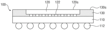
Referring to fig. 1A, a semiconductor chip 120 may be mounted on a top surface of a package substrate 110. For example, the package substrate 110 may include a Printed Circuit Board (PCB). The semiconductor chip 120 may be provided in the form of a memory chip, a logic chip, or a combination thereof. Internal terminals 122 (e.g., one or more solder balls) may be disposed between the semiconductor chip 120 and the package substrate 110 to electrically connect the semiconductor chip 120 to the package substrate 110.
Referring to fig. 1B, a molding layer 130 may be formed on the package substrate 110 to cover at least a portion of the semiconductor chip 120. The molding layer 130 may be formed to expose the top surface 120s of the semiconductor chip 120. The top surface 130s of the molding layer 130 may be coplanar with the top surface 120s of the semiconductor chip 120. As an example, the semiconductor chip 120 may be flip chip bonded on the package substrate 110. As an example, the top surface 120s may serve as an inactive surface of the semiconductor chip 120. As another example, the top surface 120s may serve as an active surface of the semiconductor chip 120. External terminals 112 (e.g., one or more solder balls) may be attached to the bottom surface of the package substrate 110. Hereinafter, for convenience, the term "base body 100" will be used to refer to a structure including the package substrate 110, the semiconductor chip 120 mounted on the package substrate 110, and the molding layer 130 covering the package substrate 110.
Referring to fig. 1C, a heat dissipation layer 140 may be formed on the substrate 100. The heat dissipation layer 140 may be formed by spraying metal powder at a high speed (e.g., sonic speed or higher) using a high-pressure gas (e.g., by a cold spray process capable of depositing a metal layer at a deposition speed higher than that of a sputtering process). As an example, the heat dissipation layer 140 may be formed by providing a mixture 82 of metal powder and gas onto the substrate 100 via the nozzle 80. In some embodiments, there is no particular limitation on the material of the metal powder, and nitrogen, helium, and/or air may be used as the gas for forming the heat dissipation layer 140.
Nozzle 80 may be moved relative to substrate 100 during formation of heat spreading layer 140. For example, the nozzle 80 may be moved at least once in a direction parallel to the top surface of the substrate 100 to supply the mixture 82 onto the substrate 100.
Referring to fig. 1D, as a result of the above-described process, the semiconductor package 11 may be manufactured to include a base 100 provided with a package substrate 110 and a semiconductor chip 120 mounted thereon, and a heat dissipation layer 140 formed on the base 100. In some embodiments, the heat dissipation layer 140 may be in direct contact with the substrate 100. For example, the heat dissipation layer 140 may be in direct contact with the top surface 120s of the semiconductor chip 120 and the top surface 130s of the molding layer 130. Since the heat dissipation layer 140 is in direct contact with the semiconductor chip 120, thermal resistance and heat loss in heat flow from the semiconductor chip 120 to the heat dissipation layer 140 can be reduced.
Unlike the embodiments described herein, the semiconductor package 11p may be manufactured to further include a heat transfer layer 136 (e.g., a Thermal Interface Material (TIM)) disposed between the base 100 and the heat dissipation layer 140, as shown in fig. 2. Generally, the heat transfer layer 136 may include a polymer material provided with a filler (e.g., metal particles). In the case of the semiconductor package 11p of fig. 2 (i.e., including the heat transfer layer 136 disposed between the semiconductor chip 120 and the heat dissipation layer 140), it is difficult to reduce the thermal resistance in the heat flow from the semiconductor chip 120 to the heat dissipation layer 140, as compared with the semiconductor package 11 of fig. 1D including the semiconductor chip 120 and the heat dissipation layer 140 in direct contact with each other. In other words, the direct contact between the semiconductor chip 120 and the heat dissipation layer 140 may provide the semiconductor package 11 with good heat dissipation characteristics.
Referring to fig. 1E, the heat dissipation layer 140 may be formed because high-speed collision of metal particles (e.g., several micrometers to several hundred micrometers in size or diameter) may cause deformation (e.g., plastic deformation) and bonding (e.g., covalent bonding) between the metal particles and the substrate 100. Accordingly, the surface of the heat dissipation layer 140 and/or the interface between the heat dissipation layer 140 and the substrate 100 may not be flat.
For example, the top surface 120s of the semiconductor chip 120 directly contacting the heat dissipation layer 140 may be an uneven surface having a first surface roughness. The top surface 130s of the molding layer 130 directly contacting the heat dissipation layer 140 may be an uneven surface having a second surface roughness. The semiconductor chip 120 may be mainly formed of silicon, and the molding layer 130 may be formed of epoxy, in which case the first surface roughness may be less than the second surface roughness.
The top surface 140s of the heat dissipation layer 140 may be an uneven surface having a third surface roughness. The third surface roughness may be substantially the same as or similar to one of the first surface roughness and the second surface roughness. In some embodiments, the third surface roughness may be different from both the first surface roughness and the second surface roughness. In some embodiments, as shown in FIG. 1F, the top surface 140s of the heat spreading layer 140 may be a flat surface. For example, after the heat dissipation layer 140 is formed, an additional process (e.g., a polishing process) may be performed on the heat dissipation layer 140 to make the top surface 140s of the heat dissipation layer 140 have a flat profile.
As shown in fig. 1E, heat spreading layer 140 may be a single layer. As an example, the heat dissipation layer 140 may be a single layer including copper (Cu). As another example, the heat dissipation layer 140 may be a single layer including at least one metal (e.g., copper (Cu), aluminum (Al), nickel (Ni), titanium (Ti), tungsten (W), tantalum (Ta), zinc (Zn), chromium (Zr), cobalt (Co), or an alloy thereof).
As shown in fig. 1G, the heat dissipation layer 140 may be a dual layer including a first heat dissipation layer 141 and a second heat dissipation layer 143. The first heat dissipation layer 141 may include a metal material that causes the first heat dissipation layer 141 to have a higher adhesive strength than that of the second heat dissipation layer 143, and the second heat dissipation layer 143 may include a metal material that causes the second heat dissipation layer 143 to have a higher thermal conductivity than that of the first heat dissipation layer 141. The first heat dissipation layer 141 may be referred to as a first metal layer, and the second heat dissipation layer 143 may be referred to as a second metal layer. For example, the first heat dissipation layer 141 may be formed of or include aluminum (Al), and the second heat dissipation layer 143 may be formed of or include copper (Cu). Since aluminum (Al) prevents copper (Cu) from diffusing, the first heat dissipation layer 141 may function as a diffusion barrier for preventing copper (Cu) from diffusing into the semiconductor chip 120.
The first heat dissipation layer 141 may be disposed on the top surface 120s of the semiconductor chip 120 and the top surface 130s of the molding layer 130, and the second heat dissipation layer 143 may be disposed on the first heat dissipation layer 141. At least one of the first and second heat dissipation layers 141 and 143 may be a single layer including one metal element or an alloy of metal elements. The interface 142s between the first and second heat dissipation layers 141 and 143 may have an uneven topography. In some embodiments, the first and second heat dissipation layers 141 and 143 may be arranged in the following manner: the thicknesses of which are the same or similar, or different from each other.
As shown in fig. 1H, the heat dissipation layer 140 may be provided to have a multi-layer structure in which the first and second heat dissipation layers 141 and 143 are alternately stacked on each other. The first heat dissipation layer 141 may include aluminum (Al) or an alloy thereof, and the second heat dissipation layer 143 may include copper (Cu) or an alloy thereof. The plurality of interfaces 142s between the first and second heat dissipation layers 141 and 143 may have an uneven topography. The first heat dissipation layer 141 may serve as the lowermost layer of the heat dissipation layer 140, and the second heat dissipation layer 143 may serve as the uppermost layer of the heat dissipation layer 140.
As another example, the first and second heat dissipation layers 141 and 143 may contain metal elements different from each other. For example, among the heat dissipation layers 140, the first heat dissipation layer 141 located at the lowermost stage may include aluminum (Al) or an alloy thereof, the second heat dissipation layer 143 located at the uppermost stage may include copper (Cu) or an alloy thereof, and each of the first and second heat dissipation layers 141 and 143 located at the intermediate stage may include one of metal elements other than aluminum and copper or an alloy thereof.
As described above with reference to fig. 1E through 1H, the features described above in relation to the heat dissipation layer 140 may be applied in the same or similar manner to all of the other embodiments of the inventive concept.
As shown in fig. 1C, the nozzle 80 may be configured to cause the mixture 82 containing the metal powder to collide with the substrate 100 at high speed. For example, the mixture 82 may have a temperature above room temperature (e.g., about 25 ℃) and below the melting point of the metal powder. As shown in fig. 1D, a heat dissipation layer 140 composed of solid metal particles may be formed as a result of the collision. Thereafter, when heat dissipation layer 140 cools down, heat dissipation layer 140 may shrink. As will be described with reference to fig. 3A and 3B, the contraction of the heat dissipation layer 140 may be used to improve the warpage properties of the semiconductor package 11.
The cold spray process is not limited to the aforementioned method of forming the metal layer using the metal powder, and the cold spray process may be performed to form the non-metal layer from a polymer powder or a powder of a mixed material. For example, the molding layer 130 may also be formed using such a cold spray process.
Fig. 3A and 3B are cross-sectional views illustrating an example of a warpage phenomenon of a semiconductor package that may occur in a method of manufacturing the semiconductor package according to some example embodiments of the inventive concepts.
As shown in fig. 3A, the heat dissipation layer 140 may be formed by disposing the mixture 82 onto the substrate 100 having a curved topography at a first temperature T1 (e.g., room temperature of 25 ℃), where the mixture 82 may be prepared to include metal powder. For example, the mixture 82 may have a second temperature T2 (e.g., a higher temperature above room temperature of 150 ℃). At a second temperature T2, heat spreading layer 140 may have the same or similar topography as substrate 100, e.g., a curved topography.
In the case where the heat dissipation layer 140 is cooled to a temperature lower than the second temperature T2 (e.g., the first temperature T1), the heat dissipation layer 140 may contract, as shown in fig. 3B. In this case, the heat dissipation layer 140 may apply a compressive force F to the substrate 100, which may be used to change the curved topography of the substrate 100 to a flat topography.
In this specification, some example embodiments of the inventive concept will be described with reference to the case in which the base 100 is convexly bent toward the heat dissipation layer 140, but example embodiments of the inventive concept may not be limited thereto. For example, as shown in fig. 5A, contraction of heat dissipation layer 140 may be used to cause a change in the warp state of substrate 100 that is convexly curved in a direction away from heat dissipation layer 140. As another example, in the case where the substrate 100 has a flat profile at room temperature, the heat dissipation layer 140 may be formed to have a flat profile.
As shown in fig. 1D, the heat dissipation layer 140 may be formed to have a uniform thickness by controlling the moving speed of the nozzle 80 and/or the spraying rate or angle of the mixture 82 of fig. 1C. In contrast, as will be described with reference to fig. 4A to 4C, the heat dissipation layer 140 may be formed to have a non-uniform thickness. For example, if there is a spatial variation in the heat generated from the substrate 100, the heat dissipation layer 140 may be formed to have a thickness depending on or proportional to such a spatial variation.
Fig. 4A to 4C are cross-sectional views illustrating examples of a heat dissipation layer that may be used in a method of manufacturing a semiconductor package according to some example embodiments of the inventive concepts.
As shown in fig. 4A, if heat is generated mainly from the central region of the base 100, the heat dissipation layer 140 may be formed in such a manner that the thickness of the heat dissipation layer 140 on the central region of the base 100 is greater than the thickness of the heat dissipation layer 140 on the edge region of the base 100. In such an embodiment, heat dissipation layer 140 may have an upwardly convex portion. As another example, as shown in fig. 4B, heat dissipation layer 140 may be formed in such a manner that the thickness of heat dissipation layer 140 on the central region of substrate 100 is smaller than the thickness of heat dissipation layer 140 on the edge region of substrate 100. As still another example, as shown in fig. 4C, the heat dissipation layer 140 may be formed to have a convex portion on one portion of the substrate 100 and a concave portion on another portion of the substrate 100, thereby having a wave-shaped portion.
In the cold spray process of fig. 1C, the heat dissipation layer 140 may be formed to have a non-uniform thickness as will be described with reference to fig. 5A to 5C. The heat dissipation layer 140 shown in fig. 5A through 5C may illustrate a metal layer coated on the package substrate 110 in a curved profile during the cold spray process of fig. 1C. In contrast, as shown in fig. 1D, the heat dissipation layer 140 shown in fig. 4A to 4C may show a metal layer in the last step of the cooling step.
Fig. 5A to 5C are top views illustrating a cold spray process of a method of manufacturing a semiconductor package according to some example embodiments of the inventive concepts.
As shown in FIG. 5A, the nozzle 80 can be moved to spray the mixture 82 onto the substrate 100 having a concavely curved topography, in which case the heat dissipation layer 140 can be formed to have a non-uniform thickness. Then, in the case where the heat dissipation layer 140 is cooled down, as shown in fig. 4A, the base 100 may be planarized such that the central region of the heat dissipation layer 140 has the maximum thickness.
As another example, as shown in fig. 5B, the heat dissipation layer 140 may be formed on the base 100 having the upwardly convex profile, in which case the heat dissipation layer 140 may have a minimum thickness in a central region thereof. Then, in the case where the heat dissipation layer 140 is cooled down, as shown in fig. 4B, the base 100 may be planarized such that the central region of the heat dissipation layer 140 has a minimum thickness.
As yet another example, as shown in FIG. 5C, a heat dissipation layer 140 may be formed on the substrate 100 having a wave-shaped topography. Then, with the heat dissipation layer 140 cooled down, as shown in fig. 4C, the substrate 100 may be planarized such that the heat dissipation layer 140 has a wave-shaped cross-sectional profile.
Fig. 6A to 6E are top views illustrating examples of heat dissipation layers that may be used in methods of manufacturing semiconductor packages according to some example embodiments of the inventive concepts.
As shown in fig. 6A to 6E, the heat dissipation layer 140 may be provided to cover at least a portion of the substrate 100 and have various planar shapes. As an example, as shown in fig. 6A, the heat dissipation layer 140 may be a single plate (a) completely covering the base 100 when viewed in a plan view, or may include a plurality of plates (B) arranged in a matrix shape so as to partially cover the base 100. In the case where the heat dissipation layer 140 is provided in the form of a single board (a), the heat dissipation layer 140 may cover not only the top surface 120s of the semiconductor chip 120 of fig. 1D but also the top surface 130s of the molding layer 130. In the case where the heat dissipation layer 140 is provided to include a plurality of boards (B), the heat dissipation layer 140 may be provided to cover a portion of the top surface 120s of the semiconductor chip 120 and a portion of the top surface 130s of the molding layer 130 of fig. 1D.
As another example, as shown in fig. 6B, the heat dissipation layer 140 may include a circular ring pattern (a) or a rectangular ring pattern (B) that partially covers the substrate 100 when viewed in a top view. As yet another example, as shown in fig. 6C, the heat dissipation layer 140 may include a plurality of parallel stripe patterns (a) or a mesh or grid pattern (B) partially covering the substrate 100. As yet another example, as shown in fig. 6D, the heat dissipation layer 140 may be a spiral pattern (a) or a rectangular spiral pattern (B) that partially covers the substrate 100. As yet another example, as shown in fig. 6E, the heat dissipation layer 140 may include a plurality of plate shapes (a) covering corners of the substrate 100 or a star pattern (B) covering a central region of the substrate 100.
Fig. 7A to 7G are sectional views illustrating a modified example of fig. 1D.
Referring to fig. 7A, the semiconductor package 11a may be manufactured to further include an insulating layer 124 disposed between the semiconductor chip 120 and the heat dissipation layer 140. For example, the heat dissipation layer 140 may be formed after the insulating layer 124 is formed to cover the top surface 120s of the semiconductor chip 120. The top surface 120s of the semiconductor chip 120 may serve as a non-active surface. In some embodiments, insulating layer 124 may be configured to electrically isolate heat spreading layer 140 from semiconductor chip 120. Therefore, a short circuit can be prevented from being formed between the semiconductor chip 120 and the heat dissipation layer 140.
Referring to fig. 7B, the semiconductor package 11B may be manufactured to further include a plurality of through electrodes 125 vertically penetrating at least a portion of the semiconductor chip 120. The top surface 120s of the semiconductor chip 120 may be used as an active surface or an inactive surface. At least one semiconductor chip having substantially the same or similar structural characteristics as those of the semiconductor chip 120 may be further disposed between the semiconductor chip 120 and the package substrate 110 and/or between the semiconductor chip 120 and the heat dissipation layer 140. The heat dissipation layer 140 may be disposed in direct contact with the top surface 120s (e.g., inactive surface) of the semiconductor chip 120, but not in direct contact with the through electrode 125 that may partially penetrate the semiconductor chip 120. In some embodiments, at least one of the through electrodes 125 may directly contact the heat dissipation layer 140. The through electrode 125 in direct contact with the heat dissipation layer 140 may serve as at least one of a thermal path and a ground path.
Referring to fig. 7C, the semiconductor package 11C may be manufactured in such a manner that the heat dissipation layer 140 is spaced apart from the top surface 120s of the semiconductor chip 120. For example, a molding layer 130 may be formed on the package substrate 110 to cover the top surface 120s of the semiconductor chip 120, and then, a heat dissipation layer 140 may be formed on the resultant structure. In some embodiments, the molding layer 130 may be disposed between the top surface 120s of the semiconductor chip 120 and the heat dissipation layer 140.
Referring to fig. 7D, the semiconductor package 11D may be manufactured in such a manner that the heat dissipation layer 140 may be used as an EMI shielding layer. In some embodiments, the package substrate 110 may include the ground pad 114 disposed on an edge region of a top surface thereof, and the molding layer 130 may be disposed to have an opening 133 exposing the ground pad 114. In some embodiments, the opening 133 may be formed by a drilling process or an etching process.
The heat dissipation layer 140 may further include a ground contact 144 formed by filling the opening 133 with metal powder. The ground contact 144 may be connected to the ground pad 114. Due to the presence of the heat dissipation layer 140, the heat dissipation characteristic, the warpage characteristic, and the EMI characteristic of the semiconductor package 11d can be improved.
Referring to fig. 7E, a semiconductor package 11E may be manufactured in such a manner that the semiconductor chip 120 is mounted on the package substrate 110 by wire bonding. For example, the package substrate 110 may include a ground pad 114 disposed on an edge region of a top surface thereof. The semiconductor chip 120 may be mounted on the package substrate 110 by the adhesive layer 126 in such a manner that the top surface 120s thereof is oriented in an upward direction. The top surface 120s of the semiconductor chip 120 may serve as an effective surface. The semiconductor chip 120 may be electrically connected to the package substrate 110 by bonding wires 128. The molding layer 130 may be disposed to expose an edge region of the package substrate 110 and have a hole 134 exposing at least a portion of the top surface 120s of the semiconductor chip 120.
Heat dissipation layer 140 may include portions that fill holes 134, and thus, heat dissipation layer 140 may be in direct contact or non-direct contact with top surface 120s of semiconductor chip 120. Heat spreading layer 140 may also include another portion that is connected to ground pad 114 of package substrate 110 to serve as a ground contact. In some embodiments, the heat dissipation layer 140 may be configured to improve heat dissipation characteristics, warpage characteristics, and EMI shielding characteristics of the semiconductor package 11 e.
Referring to fig. 7F, the semiconductor package 11F may be manufactured in such a manner that the heat dissipation layer 140 is formed to cover the side surface of the package substrate 110. For example, the ground pad 114 may be disposed on a side surface of an edge region of the package substrate 110. The heat dissipation layer 140 may extend to a side surface covering an edge region of the package substrate 110 and may be connected to the ground pad 114. Except for these differences, the semiconductor package 11f may be configured to have substantially the same features as the semiconductor package 11E of fig. 7E.
Referring to fig. 7G, the semiconductor package 11G may be manufactured to further include a conductive underfill layer 180 disposed between the package substrate 110 and the semiconductor chip 120. For example, the semiconductor chip 120 may be mounted on the package substrate 110, and then, a cold spray process may be performed to form the conductive underfill layer 180. To prevent shorts from forming between the conductive underfill layer 180 and the semiconductor chip 120 and/or between the conductive underfill layer 180 and the package substrate 110, an insulating layer 170 may also be formed between the package substrate 110 and the semiconductor chip 120 prior to forming the conductive underfill layer 180. In some embodiments, the thermal resistance between the semiconductor chip 120 and the package substrate 110 may be reduced. According to the previously described embodiments, the internal terminal 122 may be disposed on the central region of the semiconductor chip 120 to have a center pad structure, but example embodiments of the inventive concept may not be limited thereto. For example, the semiconductor chip 120 may be provided to have internal terminals disposed on an edge region of the semiconductor chip 120 and thus have an edge pad structure.
Fig. 8A to 8F are sectional views illustrating a method of manufacturing a semiconductor package according to example embodiments of the inventive concepts. Fig. 9 is a sectional view showing a semiconductor package according to a comparative example.
Referring to fig. 8A, the semiconductor chip 120 may be mounted on the package substrate 110 and the semiconductor chip 120 may be electrically connected to the package substrate 110 through the internal terminals 122. At least one lower connection terminal 128 (e.g., a solder ball) may be additionally formed on the package substrate 110. The lower connection terminal 128 may be disposed outside the semiconductor chip 120.
Referring to fig. 8B, a heat dissipation layer may be formed on the semiconductor chip 120. The heat dissipation layer 140 may be formed by the cold spray process described with reference to fig. 1C. For example, a mask 90 may be disposed on the package substrate 110 to expose the semiconductor chip 120 and shield an area other than the semiconductor chip 120. A mixture 82 of metal powder and gas may be sprayed by a nozzle 80 onto the top surface 120s of the semiconductor chip 120. The use of the cold spray process using the mask 90 may enable the heat dissipation layer 140 to be selectively or locally formed on the top surface 120s of the semiconductor chip 120.
As previously described with reference to fig. 1E to 1H, the cold spray process may cause one of the top surface 120s of the semiconductor chip 120 and the top surface 140s of the heat dissipation layer 140 to have an uneven topography. The heat dissipation layer 140 may be in direct contact with the top surface 120s of the semiconductor chip 120. In some embodiments, although the residual layer 140a may be formed on the mask 90 during the cold spray process, the residual layer 140a may be removed when the mask 90 is removed.
Referring to fig. 8C, a molding layer 130 may be formed on the package substrate 110 to cover the semiconductor chip 120 and the heat dissipation layer 140. For example, the molding layer 130 may be formed using a molding underfill process. The use of a Mold Underfill (MUF) process may enable omission of a process of forming an insulating underfill layer between the package substrate 110 and the semiconductor chip 120. As another example, the process of forming the insulating underfill layer may also be performed before forming the molding layer 130. The molding layer 130 may be formed to expose the top surface 140s of the heat dissipation layer 140. A top surface 130s of the molding layer 130 may be coplanar with a top surface 140s of the heat dissipation layer 140. The top surface 130s of the molding layer 130 may have a flatter topography than the top surface 140s of the heat dissipation layer 140 and/or the top surface 120s of the semiconductor chip 120.
Referring to fig. 8D, a drilling process or an etching process may be performed to selectively remove a portion of the molding layer 130 to form an opening 135 exposing the lower connection terminal 128. External terminals 112 (e.g., solder balls) may be attached to the bottom surface of the package substrate 110. As a result, the lower package 10 including the package substrate 110, the semiconductor chip 120 mounted on the package substrate 110, and the heat dissipation layer 140 formed on the semiconductor chip 120 can be manufactured.
Referring to fig. 8E, an upper package 20 may be provided. The upper package 20 may include: an upper package substrate 210, e.g., a Printed Circuit Board (PCB), an upper semiconductor chip 220 mounted on the upper package substrate 210, bonding wires 228 electrically connecting the semiconductor chip 220 to the upper package substrate 210, and an upper mold layer 230 covering the upper semiconductor chip 220. The upper semiconductor chip 220 may be attached to the upper package substrate 210 using an adhesive layer 226. The semiconductor chip 220 may be provided in the form of a memory chip, a logic chip, or a combination thereof. The upper package 20 may include upper connection terminals 212 aligned with the openings 135 of the molding layer 130. As another example, the upper package 20 may be provided to have substantially the same or similar structure as the lower package 10.
Referring to fig. 8F, the upper package 20 may be stacked on the lower package 10, and then a reflow process may be performed on the resulting structure. A reflow process may be performed to melt the upper connection terminals 212 and the lower connection terminals 128 of fig. 8D, and thus form connection terminals 250 electrically connecting the lower package 10 to the upper package 20. As a result, the package-on-package type semiconductor package 1 in which the upper package 20 is stacked on the lower package 10 can be manufactured.
In some embodiments, a heat dissipation layer 140 may be disposed on the semiconductor chip 120. In the case where heat dissipation layer 140 is formed of a high-rigidity material, warpage of lower package 10 can be adjusted or suppressed. Since the heat dissipation layer 140 effectively releases heat generated from the semiconductor chip 120 to the outside, the use of the heat dissipation layer 140 may enable improvement of heat dissipation characteristics of the lower package 10 and/or the semiconductor package 1. Since the thickness TH1 of the semiconductor chip 120 does not need to be increased for heat dissipation, the thickness TH4 of the semiconductor package 1 can be reduced. A technical problem associated with such thickness reduction will be described with reference to fig. 9.
Referring to fig. 9, unlike the embodiments described herein, the package-on-package type semiconductor package 1p may be manufactured to include an upper package 20 stacked on a lower package 10p, but a heat dissipation layer is not provided in the semiconductor package 1 p. In this case, in order to achieve the desired heat dissipation performance of the lower package 10p and/or the semiconductor package 1p, the thickness TH1p of the semiconductor chip 120p must be increased.
By increasing the thickness TH1p of the semiconductor chip 120p, the diffusion thermal resistance of the lower package 10p and/or the semiconductor package 1p can be reduced. This means that, in order to improve the heat dissipation characteristics of the lower package 10p and/or the semiconductor package 1p, the thickness TH1p of the semiconductor chip 120p must be increased. However, in the case where the thickness TH1p of the semiconductor chip 120p is increased in order to improve the heat dissipation performance, the thickness TH4p of the semiconductor package 1p is also increased.
In contrast, according to some example embodiments of the inventive concepts, the heat dissipation layer 140 disposed on the semiconductor chip 120 may enable a reduction in diffusion thermal resistance even when the thickness TH1 of the semiconductor chip 120 is less than the thickness TH1p of the semiconductor chip 120 p. That is, since the heat dissipation layer 140 is provided on the semiconductor chip 120, it is not necessary to increase the thickness TH1 of the semiconductor chip 120 in order to improve the heat dissipation characteristic, and therefore, the thickness TH4 of the semiconductor package 1 can be reduced or minimized.
Referring back to fig. 8F, the thickness TH2 of the heat dissipation layer 140 may be less than the thickness TH1 of the semiconductor chip 120. As an example, the thickness TH2 of the heat dissipation layer 140 may range from about 25% to about 70% of the thickness TH1 of the semiconductor chip 120. As an example, the thickness TH1 of the semiconductor chip 120 may be about 100 μm, and the thickness TH2 of the heat dissipation layer 140 may range from about 25 μm to 70 μm, but example embodiments of the inventive concept may not be limited thereto. The total thickness TH3 (i.e., TH1+ TH2) of the semiconductor chip 120 and the heat dissipation layer 140 may be less than or equal to the thickness TH1p of the semiconductor chip 120p of fig. 9. The thickness TH4 of the semiconductor package 1 may be less than or equal to the thickness TH4p of the semiconductor package 1 p.
Fig. 10A to 10B are sectional views illustrating a modified example of fig. 8F. Fig. 10C is an enlarged sectional view showing a part of fig. 10B.
Referring to fig. 10A, the semiconductor package 1a may be manufactured by stacking an upper package 20 on a lower package 10A. Some embodiments provide a lower package 10a, which may be prepared to include an insulating layer 124 disposed between a semiconductor chip 120 and a heat dissipation layer 140. By providing the insulating layer 124, short circuit can be prevented from being formed between the semiconductor chip 120 and the heat dissipation layer 140.
Referring to fig. 10B, the semiconductor package 1B may be manufactured by stacking the upper package 20 on the lower package 10B, where the lower package 10B may be prepared to include the heat dissipation layer 140B in contact with the upper package substrate 210. The heat dissipation layer 140b may allow heat generated in the semiconductor chip 120 to be effectively released to the outside through the upper package substrate 210 thereon, and thus, effective heat dissipation characteristics can be achieved. As shown in fig. 10C, the heat dissipation layer 140b may include a first metal part 140b1 having a lower melting point and a second metal part 140b2 having a higher melting point. As an example, the first metal part 140b1 may include solder, and the second metal part 140b2 may include copper. The first metal part 140b1 may enable reduction in adhesion resistance between the lower package 10b and the upper package 20, thereby enhancing adhesion strength of the heat dissipation layer 140b, and the second metal part 140b2 may enable reduction in thermal resistance, thereby enhancing heat dissipation characteristics of the heat dissipation layer 140 b.
Fig. 11A to 11D are sectional views illustrating a method of manufacturing a semiconductor package according to some example embodiments of the inventive concepts. Fig. 12A to 12C are plan views illustrating modified examples of fig. 11A to 11C. Fig. 13A is a cross-sectional view illustrating a package on package (PoP) semiconductor package including the semiconductor package of fig. 11D. Fig. 13B is a sectional view showing a modified example of fig. 13A.
Referring to fig. 11A, the semiconductor chip 120 may be mounted on the package substrate 110, and the semiconductor chip 120 may be electrically connected to the package substrate 110 via the internal terminals 122. The top surface 120s may serve as an inactive surface of the semiconductor chip 120.
Referring to fig. 11B, a cavity 121 may be provided in the semiconductor chip 120. As an example, an etching process may be performed to partially remove the top surface 120s of the semiconductor chip 120 and thus form the cavity 121 recessed in a direction from the top surface 120s of the semiconductor chip 120 toward the package substrate 110.
Referring to fig. 11C, after the insulating layer 124 is formed in the cavity 121, a heat dissipation layer 140 may be formed to fill the cavity 121. The heat dissipation layer 140 may be formed through the cold spray process described with reference to fig. 1C. The top surface 140s may serve as an uneven surface of the heat dissipation layer 140, and the top surface 120s may serve as a flat surface of the semiconductor chip 120. The interface between heat spreading layer 140 and insulating layer 124 may be an uneven surface.
Referring to fig. 11D, a molding layer 130 may be formed on the package substrate 110 to surround the semiconductor chip 120. The molding layer 130 may be formed to expose not only the top surface 140s of the heat dissipation layer 140 but also the top surface 120s of the semiconductor chip 120. A top surface 130s of the molding layer 130 may be formed to be coplanar with a top surface 140s of the heat dissipation layer 140 and/or a top surface 120s of the semiconductor chip 120. The top surface 130s of the molding layer 130 may be a flat surface. As a result of the above process, the semiconductor package 12 in which the semiconductor chip 120 embedded with the heat dissipation layer 140 is flip-chip bonded to the package substrate 110 can be manufactured. Here, since the heat dissipation layer 140 is embedded in the semiconductor chip 120, warpage of the semiconductor chip 120 can be suppressed, and further, the thickness of the semiconductor package 12 can be reduced.
Unlike the description with reference to fig. 11A to 11C, the cavity 121 and the heat dissipation layer 140 may be formed at a wafer level. For example, as shown in fig. 12A, a manufacturing process may be performed on a wafer 120w to manufacture a plurality of semiconductor chips 120. Then, as shown in fig. 12B, the surface 120ws of the wafer 120w corresponding to the top surface 120s of the semiconductor chip 120 may be selectively etched to form cavities 121 in the semiconductor chip 120, respectively. As shown in fig. 12C, an insulating layer (e.g., 124 of fig. 11C) may be formed in the cavity 212, and then, a cold spray process may be performed to form the heat dissipation layer 140 filling the cavity 121. In some embodiments, a grinding process may be performed on the surface 120ws of the wafer 120w on which the heat dissipation layer 140 is disposed to remove the insulating layer or the heat dissipation layer from areas other than the cavities 121.
A dicing process may be performed to separate the wafer 120w into the semiconductor chips 120 embedded with the heat dissipation layer 140. Then, each semiconductor chip 120 separated by the dicing process may be bonded to the package substrate 110 (e.g., in a flip chip bonding manner), and a molding layer 130 may be formed on the resultant structure. As a result, the semiconductor package 12 of fig. 11D can be manufactured.
Referring to fig. 13A, an upper package 20 may be stacked on a semiconductor package 12 (hereinafter, referred to as a lower package) to manufacture a package-on-package type semiconductor package 2. In some embodiments, the connection terminals 250 may also be formed to electrically connect the lower package 12 to the upper package 20.
Referring to fig. 13B, the semiconductor package 2a may be manufactured by stacking the upper package 20 on the lower package 12a, where the lower package 12a may be prepared to include a heat dissipation layer 140c in contact with the upper package substrate 210. Since the heat dissipation layer 140c is disposed in contact with the upper package substrate 210, the heat dissipation characteristics of the semiconductor package 2a can be improved. As previously described with reference to fig. 10C, the heat dissipation layer 140C may include metal parts having different melting points.
Fig. 14A to 14F are sectional views illustrating a method of manufacturing a semiconductor package according to some example embodiments of the inventive concepts. Fig. 14E is an enlarged sectional view illustrating a portion of fig. 14D.
Referring to fig. 14A, the semiconductor chip 120 may be mounted on the package substrate 110 and the semiconductor chip 120 may be electrically connected to the package substrate 110 via the internal terminals 122. At least one lower connection terminal 128 (e.g., a solder ball) may also be disposed on the package substrate 110. In some embodiments, the ground pad 114 may be provided on or within a side surface of the edge region of the package substrate 110. The top surface 120s of the semiconductor chip 120 may serve as a non-active surface.
Referring to fig. 14B, a molding layer 130 may be formed on the package substrate 110 to cover the semiconductor chip 120, and a portion of the molding layer 130 may be selectively removed to form an opening 135 exposing the lower connection terminal 128. For example, the molding layer 130 may be formed by a MUF process, and the opening 135 may be formed by, for example, a drilling process or an etching process. The molding layer 130 may have a top surface 130s substantially coplanar with the top surface 120s of the semiconductor chip 120. At least one external terminal 112 (e.g., a solder ball) may be attached to the bottom surface of the package substrate 110. As a result, the lower package 13 including the package substrate 110, the semiconductor chip 120 mounted on the package substrate 110, and the molding layer 130 covering the semiconductor chip 120 can be manufactured.
Referring to fig. 14C, an upper package 20 may be provided. The upper package 20 may include an upper semiconductor chip 220, the upper semiconductor chip 220 being bonded to the upper package substrate 210 via bonding wires 228, covered with an upper mold layer 230, and attached to the upper package substrate 210 by an adhesive layer 226. The upper connection terminals 212 may be disposed on the bottom surface of the upper package substrate 210 and may be aligned with the openings 135 of the molding layer 130.
Referring to fig. 14D, the upper package 20 may be stacked on the lower package 13, and then a reflow process may be performed on the resulting structure. A reflow process may be performed to melt the upper connection terminals 212 and the lower connection terminals 128 of fig. 14C, and thus form connection terminals 250 electrically connecting the lower package 13 to the upper package 20.
Then, a shielding layer 340 may be disposed to surround the lower and upper packages 13 and 20 and thus prevent and/or reduce electromagnetic interference. The shield layer 340 may be formed by a cold spray process described with reference to fig. 1C. The nozzle 80 may be configured to spray a mixture 82 of metal powder and gas on the upper package 20 in a vertical state (a). In addition, the nozzle 80 may be configured to spray the mixture 82 on the side surfaces of the lower and upper packages 13 and 20 in an inclined state (B) or a horizontal state (C).
The shielding layer 340 may be configured to have substantially the same characteristics and surface roughness as the heat dissipation layer 140 described with reference to fig. 1E through 1H. For example, the shielding layer 340 may be a single layer or a plurality of layers including copper or aluminum. At least one of the surface 340s of the shield layer 340, the interface between the shield layer 340 and the upper package 20, and the interface between the shield layer 340 and the lower package 13 may be uneven.
In some embodiments, as shown in fig. 14E, the shielding layer 340 may include a first metal part 340a and a second metal part 340 b. As an example, the first metal part 340a may include copper (Cu), and the second metal part 340b may include ferrite (ferrite). As another example, the shield layer 340 may include one of the first and second metal parts 340a and 340 b. The first and second metal parts 340a and 340b may have a size (e.g., diameter) greater than a size G of the gap 310 formed between the upper and lower packages 20 and 13. For example, the dimension G of the gap 310 may be in the range of about 10 μm to about 50 μm, and the first and second metal parts 340a and 340b may have a dimension greater than the dimension G of the gap 310. In this case, it is possible to prevent the shielding layer 340 from extending into the gap 310 and thus prevent a short circuit from being formed between the shielding layer 340 and the connection terminal 250.
Referring to fig. 14F, as a result of the above-described process, the semiconductor package 3 may be manufactured to include the lower package 13, the upper package 20 stacked on the lower package 13, and the shield layer 340 encapsulating the lower package 13 and the upper package 20. The shield layer 340 may be electrically connected to the ground pad 114. Due to the presence of the shielding layer 340, it is possible to increase the rigidity of the semiconductor package 3 and improve the EMI characteristics of the semiconductor package 3. As will be described with reference to fig. 15A to 15D, various modifications may be made to the structure of the semiconductor package 3.
Fig. 15A to 15D are sectional views showing a modified example of fig. 14F.
Referring to fig. 15A, the semiconductor package 3a may be manufactured to include an insulating layer 312, the insulating layer 312 partially filling a gap 310 between the lower package 13 and the upper package 20. As an example, the metal particles comprising shield layer 340 may have a size less than or equal to size G of gap 310, in which case some of the metal particles may flow into gap 310 to form shield layer 340 that fills at least a portion of gap 310. In the case where the shield layer 340 is formed in the gap 310, the shield layer 340 may be connected to the connection terminal 250; that is, a short circuit may be formed by the shield layer 340. In order to prevent the occurrence of short circuits, an insulating layer 312 may be additionally formed in the gap 310 to surround the connection terminal 250. The insulating layer 312 may prevent the connection terminal 250 from contacting the shield layer 340 even when the shield layer 340 is partially formed in the gap 310.
Referring to fig. 15B, the semiconductor package 3B may be manufactured to include an insulating layer 313, the insulating layer 313 completely filling the gap 310 between the lower package 13 and the upper package 20. In this case, even when the size of the metal particles constituting the shield layer 340 is smaller than the size G of the gap 310, the shield layer 340 has no chance to be formed in the gap 310.
Referring to fig. 15C, the semiconductor package 3C may be manufactured to include a package substrate 110 and a ground pad 114 disposed on an edge region of the package substrate 110. The molding layer 130 of the lower package 13 may have a size smaller than that of the package substrate 110. For example, the molding layer 130 may be formed to expose an edge region of the top surface of the package substrate 110. The shield layer 340 may extend to an exposed edge region of the top surface of the package substrate 110 and may be connected to the ground pad 114.
Referring to fig. 15D, the semiconductor package 3D may be manufactured to include a package substrate 110 in which a first ground pad 114a is disposed on a bottom surface of an edge region thereof and a second ground pad 114b is disposed on a top surface of an opposite edge region thereof. The molding layer 130 of the lower package 13 may be disposed to cover a top surface of an edge region of the package substrate 110 and expose a top surface of an opposite edge region of the package substrate 110. The shield layer 340 may be disposed to cover side surfaces of an edge region of the package substrate 110 and may be connected to the first ground pad 114a, and the shield layer 340 may be disposed to cover a top surface of an opposite edge region of the package substrate 110 and may be connected to the second ground pad 114 b.
When the package substrate 110 is rectangular in a top view, the first ground pad 114a may be disposed on a bottom surface of at least one of the four edge regions of the package substrate 110, and the second ground pad 114b may be disposed on a top surface of the other edge region of the package substrate 110. As another example, the first ground pad 114a may be disposed on a side surface of an edge region of the package substrate 110.
Fig. 16A to 16F are sectional views illustrating a method of manufacturing a semiconductor package according to some example embodiments of the inventive concepts. Fig. 16G is an enlarged plan view showing a part of fig. 16F.
Referring to fig. 16A, a semiconductor chip 120 may be mounted on a package substrate 110 (e.g., in a flip chip bonding manner) and the semiconductor chip 120 may be electrically connected to the package substrate 110 via internal terminals 122, and a molding layer 130 may be formed to surround the semiconductor chip 120. At least one lower connection terminal 128 (e.g., a solder ball) may be formed on the package substrate 110 and surround the semiconductor chip 120. For example, the molding layer 130 may be formed by a MUF process and may have a top surface 130s substantially coplanar with the top surface 120s of the semiconductor chip 120. The top surface 120s of the semiconductor chip 120 may serve as a non-active surface. At least one external terminal 112 (e.g., a solder ball) may be attached to the bottom surface of the package substrate 110.
Referring to fig. 16B, a portion of the molding layer 130 may be selectively removed to form an opening 135 exposing the lower connection terminal 128. For example, the opening 135 may be formed by a mechanical drilling process, a laser drilling process, or an etching process. After the opening 135 is formed, a cleaning process may also be performed.
Referring to fig. 16C, a metal layer 410 may be formed on the package substrate 110 to cover the semiconductor chip 120 and the molding layer 130 and to fill the opening 135. For example, the metal layer 410 may be formed using a cold spray process described with reference to fig. 1C. For example, the formation of the metal layer 410 may include: while moving the nozzle 80 in the horizontal direction, the mixture 82 of the metal powder and the gas is sprayed onto the package substrate 110. As described earlier with reference to fig. 3A and 3B, since the metal layer 410 is formed by the cold spray process, the warpage of the package substrate 110 on which the semiconductor chip 120 is mounted can be suppressed or controlled.
Referring to fig. 16D, a grinding process may be performed on the metal layer 410 to reduce the thickness of the metal layer 410. As a result of the sanding process, the top surface 410s of the metal layer 410 may have a planar or flat shape. In some embodiments, the process of reducing the thickness of the metal layer 410 may be performed using a chemical mechanical polishing process or an etch-back process. As another example, the grinding process performed on the metal layer 410 may be omitted. In this case, the top surface 140s of the metal layer 410 may have an uneven surface as described with reference to fig. 1E.
Referring to fig. 16E, the lower package 14 may be manufactured by forming an interposer (interposer)440 on the resulting structure. The interposer 440 may include a first interposer 412 and a second interposer 414 formed by patterning the metal layer 410. For example, an etching process may be performed to selectively remove a portion of the metal layer 410, and as a result of the etching process, the first interposer 412 may be formed to fill the opening 135, and the second interposer 414 may be formed on the semiconductor chip 120 to be spaced apart from the first interposer 412. The first interposer 412 may be in direct contact with the lower connection terminals 128, and the second interposer 414 may be in direct contact with the top surface 120s of the semiconductor chip 120.
The second interposer 414 may be disposed to partially or completely cover the top surface 120s of the semiconductor chip 120. Further, the second interposer 414 may extend toward the molding layer 130 to cover a portion of the top surface 130s of the molding layer 130. As shown in fig. 16G, the interposer 440 may include a plurality of first interposers 412 arranged around the second interposer 414.
In the case where the grinding process of fig. 16D is performed, at least one of the top surface 412s of the first interposer 412 and the top surface 414s of the second interposer 414 may be a flat surface. In the case where the grinding process of fig. 16D is omitted, at least one of the top surface 412s of the first interposer 412 and the top surface 414s of the second interposer 414 may be an uneven surface. As described with reference to fig. 1E, the top surface 120s of the semiconductor chip 120 may be an uneven surface regardless of the polishing process performed on the metal layer 410.
Referring to fig. 16F, the package-on-package type semiconductor package 4 may be manufactured by disposing the upper package 20 on the lower package 14. Since the upper connection terminals 212 of the upper package 20 are connected to the first interposer 412, the lower package 14 may be electrically connected to the upper package 20. The first interposer 412 may serve as contact plugs for interconnections, and the second interposer 414 may serve as a warpage prevention layer and a heat dissipation layer. In some embodiments, the formation of the second interposer 414 may be omitted. As will be described with reference to fig. 17A to 17B, various modifications may be made to the structure of the semiconductor package 4.
Fig. 17A to 17B are sectional views illustrating a modified example of fig. 16F.
Referring to fig. 17A, the semiconductor package 4a may be manufactured by stacking the upper package 20 on the lower package 14a, in which the insulating layer 124 is disposed between the semiconductor chip 120 and the second interposer 414 in the lower package 14 a. In some embodiments, due to the presence of the insulating layer 124, a short circuit can be prevented from forming between the semiconductor chip 120 and the second interposer 414.
Referring to fig. 17B, the semiconductor package 4B may be manufactured by stacking the upper package 20 on the lower package 14B including the substrate pads 113, the substrate pads 113 being disposed on an edge region of the top surface of the package substrate 110 and electrically connected to the first interposer 412. In some embodiments, the first interposer 412 may be disposed completely through the molding layer 130 and connected to the substrate pads 113.
Fig. 18A to 18E are sectional views illustrating a method of manufacturing a semiconductor package according to some example embodiments of the inventive concepts.
Referring to fig. 18A, a semiconductor chip 120 may be bonded on a package substrate 110 (e.g., flip chip bonding), and a molding layer 130 may be formed on the resulting structure (e.g., using the same or similar method as previously described with reference to fig. 16A and 16B). The passivation layer 490 may be formed to cover the top surface 130s of the molding layer 130 and have a hole 495 exposing at least a portion of the top surface 120s of the semiconductor chip 120. The top surface 120s of the semiconductor chip 120 may serve as a non-active surface. Passivation layer 490 may be formed by depositing an insulating material (e.g., silicon oxide, silicon nitride, or a polymer).
Referring to fig. 18B, an opening 135 may be formed to expose the lower connection terminal 128. As an example, the passivation layer 490 and the molding layer 130 may be partially and selectively removed through a mechanical drilling process, a laser drilling process, or an etching process, and the opening 135 may be formed as a result. After the opening 135 is formed, a cleaning process may also be performed.
Referring to fig. 18C, for example, a metal layer 410 may be formed on the package substrate 110 through a cold spray process as previously described with reference to fig. 1C. The metal layer 410 may be formed to cover the passivation layer 490 and the semiconductor chip 120 and to fill the hole 495 and the opening 135.
Referring to fig. 18D, a grinding process may be performed on the metal layer 410 to expose the passivation layer 490. The interposer 440 may be formed as a result of a polishing process performed on the metal layer 410. Further, the lower package 15 including the interposer 440 can be formed by performing a grinding process on the metal layer 410, where the interposer 440 may include a first interposer 412 and a second interposer 414, wherein the first interposer 412 is disposed to fill the opening 135 and is connected to the lower connection terminal 128, and the second interposer 414 is disposed to fill the hole 495 and is in direct contact with the semiconductor chip. As a result of the grinding process, the top surface 412s of the first interposer 412, the top surface 414s of the second interposer 414, and the top surface 490s of the passivation layer 490 may be formed to have a planar or flat shape. In contrast, the top surface 120s of the semiconductor chip 120 may have a non-planar or uneven shape as a result of the cold spray process.
The dimension S1 of the second interposer 414 may be substantially the same as the dimension S2 of the holes 495. As an example, the size S2 of the hole 495 may be smaller than the size S3 of the semiconductor chip 120, and the size S1 of the second interposer 414 may be smaller than the size S3 of the semiconductor chip 120. For example, the second interposer 414 may be formed to expose an edge region of the top surface 120s of the semiconductor chip 120.
As another example, the size S2 of the hole 495 may be substantially the same as the size S3 of the semiconductor chip 120, and the size S1 of the second interposer 414 may be substantially the same as the size S3 of the semiconductor chip 120. For example, the second interposer 414 may be formed to cover the entire area of the top surface 120s of the semiconductor chip 120.
As yet another example, the size S2 of the hole 495 may be greater than the size S3 of the semiconductor chip 120, and the size S1 of the second interposer 414 may be greater than the size S3 of the semiconductor chip 120. In this case, the second interposer 414 may be formed to also cover a portion of the molding layer 130 adjacent to the side surface of the semiconductor chip 120.
Referring to fig. 18E, the package on package type semiconductor package 5 may be manufactured by stacking the upper package 20 on the lower package 15, where the package on package type package 5 may include an interposer 440, the interposer 440 including a first interposer 412 serving as a contact plug for interconnection and a second interposer 414 serving as a heat dissipation layer and a warpage preventing layer. The first and second interposers 412, 414 may be formed to have the same or similar planar arrangement as shown in fig. 16G.
As another example, the insulating layer 124 of fig. 17A may also be disposed between the semiconductor chip 120 and the second interposer 414. As still another example, the substrate pads 113 of fig. 17B may also be disposed on an edge area of the top surface of the package substrate 110 instead of the lower connection terminals 128. In this case, the first interposer 412 may be disposed completely through the passivation layer 490 and the molding layer 130, and may be connected to the substrate pad 113.
Fig. 19A to 19E are sectional views illustrating methods of manufacturing a semiconductor package according to some example embodiments of the inventive concepts.
Referring to fig. 19A, a semiconductor chip 120 may be bonded on a package substrate 110 (e.g., a flip chip bonding method), and a molding layer 130 may be formed on the resulting structure. The molding layer 130 may cover the semiconductor chip 120. Accordingly, the top surface 130s of the molding layer 130 may be disposed at a higher level than the top surface 120s of the semiconductor chip 120. The top surface 120s of the semiconductor chip 120 may serve as a non-active surface.
Referring to fig. 19B, an opening 135 may be formed to expose the lower connection terminal 128, and a hole 137 may be formed to expose the semiconductor chip 120. As an example, the formation of the opening 135 and the hole 137 may include performing a drilling process or an etching process to selectively remove the molding layer 130. The top surface 120s of the semiconductor chip 120 may be exposed through the hole 137. After the opening 135 and the hole 137 are formed, a cleaning process may also be performed.
Referring to fig. 19C, for example, a metal layer 410 may be formed on the package substrate 110 through a cold spray process as previously described with reference to fig. 1C. The metal layer 410 may be formed to cover the semiconductor chip 120 and fill the hole 137 and the opening 135.
Referring to fig. 19D, a grinding process may be performed on the metal layer 410 to expose the top surface 130s of the molding layer 130. The interposer 440 may be formed as a result of a polishing process performed on the metal layer 410. Further, by performing a grinding process on the metal layer 410, the lower package 16 including the interposer 440 can be formed, where the interposer 440 may include a first interposer 412 and a second interposer 414, the first interposer 412 being disposed to fill the opening 135 and connected to the lower connection terminal 128, the second interposer 414 being disposed to fill the hole 137 and directly contact the semiconductor chip 120.
As a result of the sanding process, the top surface 412s of the first interposer 412, the top surface 414s of the second interposer 414, and the top surface 130s of the molding layer 130 may be formed to have a planar or flat shape. In contrast, the top surface 120s of the semiconductor chip 120 may have a non-planar or uneven shape as a result of the cold spray process. As described with reference to fig. 18D, the second interposer 414 may be sized according to the size of the hole 137.
Referring to fig. 19E, the package on package type semiconductor package 6 may be manufactured by stacking the upper package 20 on the lower package 16, where the package on package type package 6 may include an interposer 440, the interposer 440 including a first interposer 412 serving as a contact plug for interconnection and a second interposer 414 serving as a heat dissipation layer and a warpage prevention layer. The first and second interposers 412, 414 may be formed to have the same or similar planar arrangement as shown in fig. 16G.
Similar to fig. 17A, an insulating layer 124 may also be disposed between the semiconductor die 120 and the second interposer 414. Alternatively, similar to fig. 17B, the lower connection terminals 128 may not be provided, the substrate pads 113 may also be provided on an edge region of the top surface of the package substrate 110, and the first interposer 412 may be provided completely through the molding layer 130 and connected to the substrate pads 113.
According to some example embodiments of the inventive concepts, a cold spray process may be performed to form a heat dissipation layer in direct contact with a semiconductor chip, which enables it to reduce a loss of heat transfer from the semiconductor chip to the heat dissipation layer. Further, the heat dissipation layer may apply a compressive force to the semiconductor package as the heat dissipation layer cools, which may be used to inhibit or prevent the semiconductor package from suffering from warpage problems. That is, according to some example embodiments of the inventive concepts, thermal characteristics of a semiconductor package can be improved to prevent malfunction of the semiconductor package caused by warpage, thereby improving the yield of the semiconductor package.
Further, the cold spray process may be performed in such a manner that the EMI shielding layer is not formed in the gap between the upper package and the lower package of the package-on-package type semiconductor package. Accordingly, the EMI shielding layer can be prevented from being in contact with the connection terminals of the upper and lower packages. That is, a short circuit through the EMI shielding layer can be prevented, thereby improving the electrical characteristics of the semiconductor package. In addition, a cold spray process may be performed to form an interposer on the lower package, the interposer may enable an electrical connection path to be formed between the upper package and the lower package, and in addition, heat dissipation characteristics and warpage characteristics of the lower package may be improved.
While certain exemplary embodiments of the inventive concept have been particularly shown and described, it will be understood by those of ordinary skill in the art that various changes in form and details may be made therein without departing from the spirit and scope of the appended claims.