CN115015345A - Non-modified flexible electrochemical sensor for rapidly detecting heavy metal ions and preparation method and application thereof - Google Patents
Non-modified flexible electrochemical sensor for rapidly detecting heavy metal ions and preparation method and application thereof Download PDFInfo
- Publication number
- CN115015345A CN115015345A CN202210943951.7A CN202210943951A CN115015345A CN 115015345 A CN115015345 A CN 115015345A CN 202210943951 A CN202210943951 A CN 202210943951A CN 115015345 A CN115015345 A CN 115015345A
- Authority
- CN
- China
- Prior art keywords
- lig
- electrode
- detection
- scribing
- electrodes
- Prior art date
- Legal status (The legal status is an assumption and is not a legal conclusion. Google has not performed a legal analysis and makes no representation as to the accuracy of the status listed.)
- Granted
Links
- 150000002500 ions Chemical class 0.000 title claims abstract description 59
- 238000002360 preparation method Methods 0.000 title claims abstract description 49
- 229910001385 heavy metal Inorganic materials 0.000 title claims abstract description 43
- 238000001514 detection method Methods 0.000 claims abstract description 104
- 238000000034 method Methods 0.000 claims abstract description 35
- 239000000758 substrate Substances 0.000 claims abstract description 26
- 229920005570 flexible polymer Polymers 0.000 claims abstract description 25
- OKTJSMMVPCPJKN-UHFFFAOYSA-N Carbon Chemical compound [C] OKTJSMMVPCPJKN-UHFFFAOYSA-N 0.000 claims abstract description 16
- 229910021389 graphene Inorganic materials 0.000 claims abstract description 14
- 239000000463 material Substances 0.000 claims abstract description 9
- 238000000576 coating method Methods 0.000 claims abstract description 6
- 238000004140 cleaning Methods 0.000 claims abstract description 5
- 239000011248 coating agent Substances 0.000 claims abstract description 3
- 238000005520 cutting process Methods 0.000 claims abstract description 3
- 238000001035 drying Methods 0.000 claims abstract 2
- 238000009413 insulation Methods 0.000 claims abstract 2
- 238000003825 pressing Methods 0.000 claims abstract 2
- 238000005171 square wave anodic stripping voltammetry Methods 0.000 claims description 38
- 238000007639 printing Methods 0.000 claims description 23
- 238000002484 cyclic voltammetry Methods 0.000 claims description 21
- 238000000151 deposition Methods 0.000 claims description 20
- 230000008021 deposition Effects 0.000 claims description 20
- 238000003763 carbonization Methods 0.000 claims description 14
- 239000000243 solution Substances 0.000 claims description 10
- 239000000872 buffer Substances 0.000 claims description 9
- 239000008351 acetate buffer Substances 0.000 claims description 7
- 238000004519 manufacturing process Methods 0.000 claims description 7
- 238000011049 filling Methods 0.000 claims description 6
- 239000011347 resin Substances 0.000 claims description 5
- 229920005989 resin Polymers 0.000 claims description 5
- 238000001237 Raman spectrum Methods 0.000 claims description 4
- 239000012535 impurity Substances 0.000 claims description 4
- 229920000307 polymer substrate Polymers 0.000 claims description 4
- 239000011148 porous material Substances 0.000 claims description 4
- 229910052799 carbon Inorganic materials 0.000 claims description 3
- 229910052757 nitrogen Inorganic materials 0.000 claims description 3
- 229910052760 oxygen Inorganic materials 0.000 claims description 2
- 230000001360 synchronised effect Effects 0.000 claims description 2
- 239000004973 liquid crystal related substance Substances 0.000 claims 2
- 238000000016 photochemical curing Methods 0.000 claims 2
- 230000008569 process Effects 0.000 abstract description 27
- 238000012986 modification Methods 0.000 abstract description 12
- 230000004048 modification Effects 0.000 abstract description 12
- 239000002086 nanomaterial Substances 0.000 abstract description 8
- 230000007613 environmental effect Effects 0.000 abstract description 3
- 238000012360 testing method Methods 0.000 description 34
- 230000001965 increasing effect Effects 0.000 description 24
- 238000004090 dissolution Methods 0.000 description 21
- 238000010586 diagram Methods 0.000 description 20
- 238000001878 scanning electron micrograph Methods 0.000 description 17
- XLYOFNOQVPJJNP-UHFFFAOYSA-N water Substances O XLYOFNOQVPJJNP-UHFFFAOYSA-N 0.000 description 16
- 230000000694 effects Effects 0.000 description 14
- 239000010410 layer Substances 0.000 description 14
- 230000007423 decrease Effects 0.000 description 13
- 230000003247 decreasing effect Effects 0.000 description 11
- 230000008859 change Effects 0.000 description 10
- 238000002474 experimental method Methods 0.000 description 10
- 238000005457 optimization Methods 0.000 description 8
- 238000012512 characterization method Methods 0.000 description 7
- 239000000047 product Substances 0.000 description 7
- 230000004044 response Effects 0.000 description 7
- ATJFFYVFTNAWJD-UHFFFAOYSA-N Tin Chemical compound [Sn] ATJFFYVFTNAWJD-UHFFFAOYSA-N 0.000 description 5
- 238000004458 analytical method Methods 0.000 description 5
- 238000005452 bending Methods 0.000 description 5
- 230000015572 biosynthetic process Effects 0.000 description 5
- 238000011088 calibration curve Methods 0.000 description 5
- 238000013461 design Methods 0.000 description 5
- 238000005516 engineering process Methods 0.000 description 5
- 230000009467 reduction Effects 0.000 description 5
- 230000002829 reductive effect Effects 0.000 description 5
- 230000035945 sensitivity Effects 0.000 description 5
- 238000004833 X-ray photoelectron spectroscopy Methods 0.000 description 4
- WLZRMCYVCSSEQC-UHFFFAOYSA-N cadmium(2+) Chemical compound [Cd+2] WLZRMCYVCSSEQC-UHFFFAOYSA-N 0.000 description 4
- 230000002452 interceptive effect Effects 0.000 description 4
- 229920001721 polyimide Polymers 0.000 description 4
- QTBSBXVTEAMEQO-UHFFFAOYSA-N Acetic acid Chemical compound CC(O)=O QTBSBXVTEAMEQO-UHFFFAOYSA-N 0.000 description 3
- 238000001069 Raman spectroscopy Methods 0.000 description 3
- 229910021607 Silver chloride Inorganic materials 0.000 description 3
- 230000009286 beneficial effect Effects 0.000 description 3
- 239000003153 chemical reaction reagent Substances 0.000 description 3
- 230000000052 comparative effect Effects 0.000 description 3
- 235000020188 drinking water Nutrition 0.000 description 3
- 239000003651 drinking water Substances 0.000 description 3
- 238000000835 electrochemical detection Methods 0.000 description 3
- 239000007788 liquid Substances 0.000 description 3
- 229910052751 metal Inorganic materials 0.000 description 3
- 239000002184 metal Substances 0.000 description 3
- 239000000203 mixture Substances 0.000 description 3
- 238000011084 recovery Methods 0.000 description 3
- 230000027756 respiratory electron transport chain Effects 0.000 description 3
- HKZLPVFGJNLROG-UHFFFAOYSA-M silver monochloride Chemical compound [Cl-].[Ag+] HKZLPVFGJNLROG-UHFFFAOYSA-M 0.000 description 3
- 231100000331 toxic Toxicity 0.000 description 3
- 230000002588 toxic effect Effects 0.000 description 3
- 239000004642 Polyimide Substances 0.000 description 2
- 238000003848 UV Light-Curing Methods 0.000 description 2
- 229910045601 alloy Inorganic materials 0.000 description 2
- 239000000956 alloy Substances 0.000 description 2
- 230000007547 defect Effects 0.000 description 2
- 238000002848 electrochemical method Methods 0.000 description 2
- 230000002349 favourable effect Effects 0.000 description 2
- 239000007789 gas Substances 0.000 description 2
- 230000036541 health Effects 0.000 description 2
- 230000002209 hydrophobic effect Effects 0.000 description 2
- 230000006872 improvement Effects 0.000 description 2
- 238000007648 laser printing Methods 0.000 description 2
- 238000005259 measurement Methods 0.000 description 2
- 239000012528 membrane Substances 0.000 description 2
- 239000011259 mixed solution Substances 0.000 description 2
- 239000005416 organic matter Substances 0.000 description 2
- 238000013021 overheating Methods 0.000 description 2
- 238000011056 performance test Methods 0.000 description 2
- 239000000276 potassium ferrocyanide Substances 0.000 description 2
- 239000002243 precursor Substances 0.000 description 2
- 238000001179 sorption measurement Methods 0.000 description 2
- 238000011895 specific detection Methods 0.000 description 2
- 230000003595 spectral effect Effects 0.000 description 2
- 238000003950 stripping voltammetry Methods 0.000 description 2
- 239000000126 substance Substances 0.000 description 2
- 239000002344 surface layer Substances 0.000 description 2
- 239000008399 tap water Substances 0.000 description 2
- 235000020679 tap water Nutrition 0.000 description 2
- 229910021642 ultra pure water Inorganic materials 0.000 description 2
- 239000012498 ultrapure water Substances 0.000 description 2
- LFQSCWFLJHTTHZ-UHFFFAOYSA-N Ethanol Chemical compound CCO LFQSCWFLJHTTHZ-UHFFFAOYSA-N 0.000 description 1
- 229910020159 Pb—Cd Inorganic materials 0.000 description 1
- XOLBLPGZBRYERU-UHFFFAOYSA-N SnO2 Inorganic materials O=[Sn]=O XOLBLPGZBRYERU-UHFFFAOYSA-N 0.000 description 1
- FAPWRFPIFSIZLT-UHFFFAOYSA-M Sodium chloride Chemical compound [Na+].[Cl-] FAPWRFPIFSIZLT-UHFFFAOYSA-M 0.000 description 1
- 230000004913 activation Effects 0.000 description 1
- 238000003968 anodic stripping voltammetry Methods 0.000 description 1
- QVGXLLKOCUKJST-UHFFFAOYSA-N atomic oxygen Chemical compound [O] QVGXLLKOCUKJST-UHFFFAOYSA-N 0.000 description 1
- 229910052797 bismuth Inorganic materials 0.000 description 1
- JCXGWMGPZLAOME-UHFFFAOYSA-N bismuth atom Chemical compound [Bi] JCXGWMGPZLAOME-UHFFFAOYSA-N 0.000 description 1
- 239000007853 buffer solution Substances 0.000 description 1
- 229910002091 carbon monoxide Inorganic materials 0.000 description 1
- 230000003197 catalytic effect Effects 0.000 description 1
- 229910052729 chemical element Inorganic materials 0.000 description 1
- 238000002425 crystallisation Methods 0.000 description 1
- 230000008025 crystallization Effects 0.000 description 1
- 230000032798 delamination Effects 0.000 description 1
- 238000011161 development Methods 0.000 description 1
- 230000003292 diminished effect Effects 0.000 description 1
- 238000007922 dissolution test Methods 0.000 description 1
- 230000005518 electrochemistry Effects 0.000 description 1
- 238000004070 electrodeposition Methods 0.000 description 1
- 230000002708 enhancing effect Effects 0.000 description 1
- 239000003344 environmental pollutant Substances 0.000 description 1
- 238000001914 filtration Methods 0.000 description 1
- 235000013305 food Nutrition 0.000 description 1
- 239000003292 glue Substances 0.000 description 1
- 229910002804 graphite Inorganic materials 0.000 description 1
- 239000010439 graphite Substances 0.000 description 1
- 238000011065 in-situ storage Methods 0.000 description 1
- 230000006698 induction Effects 0.000 description 1
- 238000001095 inductively coupled plasma mass spectrometry Methods 0.000 description 1
- 238000002347 injection Methods 0.000 description 1
- 239000007924 injection Substances 0.000 description 1
- 229910000765 intermetallic Inorganic materials 0.000 description 1
- 238000003475 lamination Methods 0.000 description 1
- 229910044991 metal oxide Inorganic materials 0.000 description 1
- 238000002385 metal-ion deposition Methods 0.000 description 1
- 229910052752 metalloid Inorganic materials 0.000 description 1
- 150000002738 metalloids Chemical class 0.000 description 1
- 150000002739 metals Chemical class 0.000 description 1
- 238000000465 moulding Methods 0.000 description 1
- 238000013433 optimization analysis Methods 0.000 description 1
- 230000008520 organization Effects 0.000 description 1
- 238000007254 oxidation reaction Methods 0.000 description 1
- 239000001301 oxygen Substances 0.000 description 1
- 230000036961 partial effect Effects 0.000 description 1
- 238000000059 patterning Methods 0.000 description 1
- 238000007747 plating Methods 0.000 description 1
- 230000010287 polarization Effects 0.000 description 1
- 231100000719 pollutant Toxicity 0.000 description 1
- 239000002244 precipitate Substances 0.000 description 1
- 238000001556 precipitation Methods 0.000 description 1
- 238000012545 processing Methods 0.000 description 1
- 230000001737 promoting effect Effects 0.000 description 1
- 238000012372 quality testing Methods 0.000 description 1
- 238000011946 reduction process Methods 0.000 description 1
- 238000011160 research Methods 0.000 description 1
- 238000005096 rolling process Methods 0.000 description 1
- 150000003839 salts Chemical class 0.000 description 1
- 238000007650 screen-printing Methods 0.000 description 1
- 230000009528 severe injury Effects 0.000 description 1
- 229910052709 silver Inorganic materials 0.000 description 1
- 239000011780 sodium chloride Substances 0.000 description 1
- 238000010183 spectrum analysis Methods 0.000 description 1
- 230000003068 static effect Effects 0.000 description 1
- 230000007847 structural defect Effects 0.000 description 1
- 238000006467 substitution reaction Methods 0.000 description 1
- 238000003786 synthesis reaction Methods 0.000 description 1
- XOGGUFAVLNCTRS-UHFFFAOYSA-N tetrapotassium;iron(2+);hexacyanide Chemical compound [K+].[K+].[K+].[K+].[Fe+2].N#[C-].N#[C-].N#[C-].N#[C-].N#[C-].N#[C-] XOGGUFAVLNCTRS-UHFFFAOYSA-N 0.000 description 1
- -1 tin dioxide metal oxide Chemical class 0.000 description 1
- 238000004506 ultrasonic cleaning Methods 0.000 description 1
- 239000000052 vinegar Substances 0.000 description 1
- 235000021419 vinegar Nutrition 0.000 description 1
Images


Classifications
-
- G—PHYSICS
- G01—MEASURING; TESTING
- G01N—INVESTIGATING OR ANALYSING MATERIALS BY DETERMINING THEIR CHEMICAL OR PHYSICAL PROPERTIES
- G01N27/00—Investigating or analysing materials by the use of electric, electrochemical, or magnetic means
- G01N27/26—Investigating or analysing materials by the use of electric, electrochemical, or magnetic means by investigating electrochemical variables; by using electrolysis or electrophoresis
- G01N27/28—Electrolytic cell components
- G01N27/30—Electrodes, e.g. test electrodes; Half-cells
- G01N27/308—Electrodes, e.g. test electrodes; Half-cells at least partially made of carbon
-
- G—PHYSICS
- G01—MEASURING; TESTING
- G01N—INVESTIGATING OR ANALYSING MATERIALS BY DETERMINING THEIR CHEMICAL OR PHYSICAL PROPERTIES
- G01N27/00—Investigating or analysing materials by the use of electric, electrochemical, or magnetic means
- G01N27/26—Investigating or analysing materials by the use of electric, electrochemical, or magnetic means by investigating electrochemical variables; by using electrolysis or electrophoresis
- G01N27/416—Systems
- G01N27/48—Systems using polarography, i.e. measuring changes in current under a slowly-varying voltage
Landscapes
- Chemical & Material Sciences (AREA)
- Life Sciences & Earth Sciences (AREA)
- Health & Medical Sciences (AREA)
- Physics & Mathematics (AREA)
- Chemical Kinetics & Catalysis (AREA)
- Electrochemistry (AREA)
- Molecular Biology (AREA)
- Analytical Chemistry (AREA)
- Biochemistry (AREA)
- General Health & Medical Sciences (AREA)
- General Physics & Mathematics (AREA)
- Immunology (AREA)
- Pathology (AREA)
- Battery Electrode And Active Subsutance (AREA)
Abstract
Description
技术领域technical field
本发明涉及柔性电化学传感器技术领域,特别涉及一种用于重金属离子快速检测的柔性电化学传感器及其制备方法和应用。The invention relates to the technical field of flexible electrochemical sensors, in particular to a flexible electrochemical sensor for rapid detection of heavy metal ions, and a preparation method and application thereof.
背景技术Background technique
随着人口增长、工业化发展和自然资源的不合理利用等原因,重金属离子已成为释放最多的污染物之一。重金属是指密度大于5 g/cm3的金属和类金属,人体吸收重金属离子后会在体内积累增加,不可被生物降解,食用重金属超标的食物和水将对人体健康构成威胁。With population growth, industrialization development and unreasonable utilization of natural resources, heavy metal ions have become one of the most released pollutants. Heavy metals refer to metals and metalloids with a density greater than 5 g/cm 3 . After the human body absorbs heavy metal ions, it will accumulate in the body and cannot be biodegraded. Eating food and water with excessive heavy metals will pose a threat to human health.
目前传统重金属离子检测方法主要以光谱分析原理为主,虽具有良好的灵敏度和选择性,但由于设备昂贵、操作复杂且难度大,单次检测时间较长,很难适应批量和现场检测要求,因此多应用于实验室检测。电化学方法具有简单可靠、灵敏度高、适用于现场检测的特点,通过搭配快速检测仪能够实现重金属离子的快速现场检测。At present, traditional heavy metal ion detection methods are mainly based on the principle of spectral analysis. Although they have good sensitivity and selectivity, they are difficult to meet the requirements of batch and on-site detection due to expensive equipment, complex and difficult operation, and long single detection time. Therefore, it is mostly used in laboratory testing. The electrochemical method has the characteristics of simplicity, reliability, high sensitivity, and is suitable for on-site detection. The rapid on-site detection of heavy metal ions can be achieved by matching with a rapid detector.
对于新型电化学传感器的制备技术,目前已经实现了商业化和批量生产能力,商业程度和稳定性能良好。对于电化学传感器的制备方面,现有制备电化学传感器的专利多为利用丝网印刷技术实现电化学三电极的快速制备,但目前的研究仍存在专一性不强的问题。特别是用于重金属离子检测的电化学传感器,尽管目前的检测限和检测性能较为稳定,但用于Cd2+、Pb2+快速检测的电化学传感器的制备多采用对纳米材料进行改性的技术,需要额外修饰纳米材料才能实现重金属离子的特异性痕量检测。而纳米材料的制备可能会用到有毒试剂,且较为繁琐的纳米材料修饰过程大大延长了检测的准备时间,对于快速检测来说是很大的短板。For the preparation technology of new electrochemical sensors, commercialization and mass production capacity have been achieved, and the commercial degree and stability are good. For the preparation of electrochemical sensors, most of the existing patents for the preparation of electrochemical sensors are to use screen printing technology to realize the rapid preparation of electrochemical three-electrode, but the current research still has the problem of low specificity. Especially for the electrochemical sensors for heavy metal ion detection, although the current detection limit and detection performance are relatively stable, the preparation of electrochemical sensors for the rapid detection of Cd 2+ and Pb 2+ mostly adopts the modified nanomaterials. This technique requires additional modification of nanomaterials to achieve specific trace detection of heavy metal ions. The preparation of nanomaterials may use toxic reagents, and the cumbersome nanomaterial modification process greatly prolongs the preparation time for detection, which is a big shortcoming for rapid detection.
对于利用激光诱导石墨烯技术实现电化学传感器的制备和重金属离子的痕量检测研究,现有技术报道较少。For the preparation of electrochemical sensors and the trace detection of heavy metal ions using laser-induced graphene technology, there are few reports in the prior art.
CN112611794B号中国专利文献公开了一种重金属离子电化学传感器批量制备方法,该方法是先配制对目标重金属离子溶出伏安检测具有特殊催化属性的纳米敏感涂层合成所需的前驱体,然后对传感器进行图案化和结构化设计,并对激光诱导参数进行设置;通过滚动方式,将激光束对连续移动的前驱体进行刻蚀,制备对电极和修饰有特殊纳米敏感涂层的工作电极;在集成有对电极和工作电极的柔性基底上印制参比电极,构建重金属离子电化学传感器。该专利主要侧重于激光诱导石墨烯用于重金属电化学传感器的批量制备,尽管提出了一种较为笼统的制备方法,但对于不同类型的重金属离子检测,多个方面的因素都会直接影响传感器的检测效果,该专利关注的激光诱导参数存在一定的片面性,导致制备的传感器还需要配合修饰材料的修饰和改进才能达到预期的检测效果。CN112611794B Chinese patent document discloses a batch preparation method of heavy metal ion electrochemical sensors. The method is to prepare the precursors required for the synthesis of nano-sensitive coatings with special catalytic properties for the stripping voltammetry detection of target heavy metal ions, and then prepare the sensor for the sensor. Carry out patterning and structural design, and set the laser-induced parameters; by rolling the laser beam to etch the continuously moving precursor to prepare the counter electrode and the working electrode modified with a special nano-sensitive coating; in the integrated A reference electrode is printed on a flexible substrate with a counter electrode and a working electrode to construct an electrochemical sensor for heavy metal ions. The patent mainly focuses on the batch preparation of laser-induced graphene for heavy metal electrochemical sensors. Although a relatively general preparation method is proposed, for the detection of different types of heavy metal ions, various factors will directly affect the detection of the sensor. As a result, the laser-induced parameters concerned in this patent have a certain one-sidedness, so that the prepared sensor needs to be modified and improved with modification materials to achieve the expected detection effect.
CN113325053A号中国专利文献公开了一种镉离子电化学传感器工作电极及其制备、检测方法和应用,该镉离子电化学传感器工作电极包括激光诱导石墨烯(LIG)电极以及在其表面修饰的锡膜;锡膜的主体为金属锡,金属锡的表面形成有二氧化锡金属氧化物膜;LIG电极可以采用聚酰亚胺膜为基底,利用激光诱导技术刻蚀聚酰亚胺膜后制备得到;锡膜可以通过将LIG电极浸入Sn(Ⅱ)溶液中采用恒电位法沉积形成。该专利是将激光诱导石墨烯制备的工作电极与外接参比电极和对电极结合使用,且激光诱导石墨烯制备的LIG工作电极仅作为基底材料使用,该专利能够实现镉离子的痕量电化学检测主要是利用Sn膜的修饰实现的,主要工作和创新同样是在纳米材料的修饰和制备步骤。CN113325053A Chinese patent document discloses a cadmium ion electrochemical sensor working electrode and its preparation, detection method and application. The cadmium ion electrochemical sensor working electrode includes a laser-induced graphene (LIG) electrode and a tin film modified on its surface. ; The main body of the tin film is metal tin, and a tin dioxide metal oxide film is formed on the surface of the metal tin; the LIG electrode can be prepared by using a polyimide film as a substrate, and using laser induction technology to etch the polyimide film; Tin films can be formed by potentiostatic deposition by immersing LIG electrodes in Sn(II) solution. In this patent, the working electrode prepared by laser-induced graphene is used in combination with an external reference electrode and a counter electrode, and the LIG working electrode prepared by laser-induced graphene is only used as a base material. This patent can realize trace electrochemistry of cadmium ions. The detection is mainly realized by the modification of Sn film, and the main work and innovation are also in the modification and preparation steps of nanomaterials.
此外,现有技术中虽然也偶有提到采用无修饰电化学传感器进行检测的实例,但检测效果不佳,绝大部分都是作为对比例以突出镀膜传感器的检测效果,现有的无修饰电化学传感器在检测灵敏度、检测精度等方面都难以满足我们快速、方便、高效检测的应用要求。因此,如何提供一种高效、方便制备的无修饰柔性电化学传感器,能够随时方便制备、简化操作应用且同时能够高精度检测出特定类型的重金属离子,这是我们需要解决的具体技术难题。In addition, although there are occasional examples of using unmodified electrochemical sensors for detection in the prior art, the detection effect is not good, and most of them are used as comparative examples to highlight the detection effect of coated sensors. Electrochemical sensors are difficult to meet our application requirements for fast, convenient and efficient detection in terms of detection sensitivity and detection accuracy. Therefore, how to provide an efficient and easy-to-prepare unmodified flexible electrochemical sensor that can be easily prepared at any time, simplifies operation and application, and can detect specific types of heavy metal ions with high precision is a specific technical problem that we need to solve.
发明内容SUMMARY OF THE INVENTION
针对现有技术中的缺陷,本发明提出一种用于快速检测重金属离子的无修饰柔性电化学传感器及其制备方法和应用,该无修饰柔性电化学传感器具有制备简单、环保的显著特点,在实际应用中无需进行额外纳米材料的修饰和电极的预处理过程,能够有效提高电化学传感器实际应用过程中的检测效率,且传感器具备一定的柔性检测性能,能够满足不同场景下的检测需求。In view of the defects in the prior art, the present invention proposes an unmodified flexible electrochemical sensor for rapid detection of heavy metal ions, a preparation method and application thereof, and the unmodified flexible electrochemical sensor has the remarkable characteristics of simple preparation and environmental protection. In practical applications, there is no need for additional nanomaterial modification and electrode pretreatment process, which can effectively improve the detection efficiency of electrochemical sensors in practical applications, and the sensor has certain flexible detection performance, which can meet the detection needs in different scenarios.
本发明提出的技术方案为一种用于快速检测重金属离子的无修饰柔性电化学传感器,所述柔性电化学传感器包括柔性聚合物基底和设置于前述柔性聚合物基底上的三电极,所述三电极包含工作电极、参比电极和对电极,所述工作电极、参比电极和对电极均是由激光诱导石墨烯制成的LIG电极;所述柔性电化学传感器上不含用于匹配重金属离子的修饰性材料或涂层。The technical solution proposed by the present invention is an unmodified flexible electrochemical sensor for rapid detection of heavy metal ions. The flexible electrochemical sensor includes a flexible polymer substrate and three electrodes arranged on the flexible polymer substrate. The electrode comprises a working electrode, a reference electrode and a counter electrode, and the working electrode, the reference electrode and the counter electrode are all LIG electrodes made of laser-induced graphene; the flexible electrochemical sensor does not contain heavy metal ions for matching decorative materials or coatings.
本发明的上述技术方案基于以下原理:通过反复的实验发现,在柔性聚合物基底上制备的三电极,且三电极均是由激光诱导石墨烯工艺一次性成型获得的LIG电极,通过对特定工艺参数精确选取和优化控制改变了电极的微观形貌、构造、孔隙及元素组成等,使得本发明的电化学传感器在不预先涂覆用于匹配重金属离子的修饰性材料或涂层的前提下,能够有效提高电化学传感器实际应用过程中的检测效率,且具备一定的柔性检测性能,能够满足不同场景下的检测需求。The above technical solution of the present invention is based on the following principles: through repeated experiments, it is found that the three electrodes prepared on the flexible polymer substrate are LIG electrodes obtained by one-time molding of the laser-induced graphene process. The precise selection and optimal control of parameters change the microscopic morphology, structure, pores and elemental composition of the electrode, so that the electrochemical sensor of the present invention does not need to be pre-coated with modified materials or coatings for matching heavy metal ions. It can effectively improve the detection efficiency in the practical application process of the electrochemical sensor, and has a certain flexible detection performance, which can meet the detection requirements in different scenarios.
上述的无修饰柔性电化学传感器,所述LIG电极形成的碳化层均高于聚合物基底的上表面,且碳化层呈絮状结构,有致密均匀孔隙。现有的LIG电化学传感器如果不进行修饰,一般能清楚看到LIG的形状呈片状且为蜂窝形状排列,这样的结构仅能基本满足LIG作为导电基底的要求,但是为了满足痕量检测要求依然需要对LIG进行修饰(例如电沉积Sn膜等措施),而本发明制备的LIG电极表层呈絮状或绒丝状,片状结构可能被遮掩在絮状结构下层,因此可以大大增加电极表面粗糙度、增加比表面积、增加氧化还原位点以提升重金属离子的吸附。In the above-mentioned unmodified flexible electrochemical sensor, the carbonized layer formed by the LIG electrode is higher than the upper surface of the polymer substrate, and the carbonized layer has a flocculent structure with dense and uniform pores. If the existing LIG electrochemical sensors are not modified, it is generally clear that the shape of LIG is sheet-like and arranged in a honeycomb shape. Such a structure can only basically meet the requirements of LIG as a conductive substrate, but in order to meet the requirements of trace detection. It is still necessary to modify the LIG (such as electrodeposition of Sn film and other measures), but the surface layer of the LIG electrode prepared by the present invention is flocculent or filiform, and the sheet-like structure may be hidden in the lower layer of the flocculent structure, so the electrode surface can be greatly increased. Roughness, increased specific surface area, increased redox sites to improve the adsorption of heavy metal ions.
上述的无修饰柔性电化学传感器,优选的,所述LIG电极表面可检测到C1s峰、O1s峰和N1s峰,且C元素质量百分比含量在95%以上,O元素质量百分比含量在3%以下,N元素质量百分比含量在2%以下。In the above-mentioned unmodified flexible electrochemical sensor, preferably, C1s peak, O1s peak and N1s peak can be detected on the surface of the LIG electrode, and the mass percentage content of C element is more than 95%, and the mass percentage content of O element is less than 3%, The mass percentage of N element is below 2%.
上述的无修饰柔性电化学传感器,优选的,所述聚合物基底选用PI膜;所述LIG表面接触角达到90°以上且呈现疏水性。In the above-mentioned unmodified flexible electrochemical sensor, preferably, the polymer substrate is a PI film; the surface contact angle of the LIG reaches more than 90° and exhibits hydrophobicity.
上述的无修饰柔性电化学传感器,优选的,所述LIG电极拉曼光谱图像的定量信息如下:ID/IG为1.05以下,I2D/IG为1.0以上,且FWHMG为70以下。In the above-mentioned unmodified flexible electrochemical sensor, preferably, the quantitative information of the Raman spectrum image of the LIG electrode is as follows: ID / IG is less than 1.05, I 2D / IG is more than 1.0, and FWHMG is less than 70.
作为一个总的技术构思,本发明还提供一种用于快速检测重金属离子的无修饰柔性电化学传感器的制备方法,包括以下步骤:As a general technical concept, the present invention also provides a preparation method of an unmodified flexible electrochemical sensor for rapidly detecting heavy metal ions, comprising the following steps:
S1:将多层(优选三层)柔性聚合物薄膜进行粘接后,进行压膜处理,得到兼顾柔性和厚度的柔性聚合物基底;S1: After bonding the multi-layer (preferably three-layer) flexible polymer films, lamination treatment is performed to obtain a flexible polymer substrate with both flexibility and thickness;
S2:将步骤S1制备的柔性聚合物基底剪裁成电极片,将电极片超声清洗直到柔性聚合物基底表面基本无杂质;S2: cutting the flexible polymer substrate prepared in step S1 into electrode sheets, and ultrasonically cleaning the electrode sheets until the surface of the flexible polymer substrate is substantially free of impurities;
S3:利用激光诱导石墨烯技术在所述柔性聚合物基底进行LIG三电极的制备,包括:先在柔性聚合物基底上设计三电极打印轮廓,然后利用填充功能对三电极及其导线进行填充划线,再同时控制激光功率、划线间距、划线速度和激光频率,得到特定结构组分及微观形貌的LIG三电极,再对LIG三电极进行绝缘处理,干燥,得到无修饰柔性电化学传感器。S3: Use the laser-induced graphene technology to prepare the three-electrode LIG on the flexible polymer substrate, including: first designing the three-electrode printing outline on the flexible polymer substrate, and then using the filling function to fill and scribe the three-electrode and its wires Then, the laser power, scribing distance, scribing speed and laser frequency are controlled at the same time to obtain LIG three electrodes with specific structural components and microscopic morphology, and then the LIG three electrodes are insulated and dried to obtain unmodified flexible electrochemical sensor.
本发明上述方法的主要改进在于通过在柔性聚合物基底上设计三电极打印轮廓,然后利用填充功能对三电极及其导线进行填充划线,再同时综合控制激光功率、划线间距、划线速度和激光频率,进而得到特定结构组分及微观形貌的LIG三电极。The main improvement of the above method of the present invention is to design the outline of the three-electrode printing on the flexible polymer substrate, and then use the filling function to fill and scribe the three electrodes and their wires, and then comprehensively control the laser power, scribing spacing and scribing speed at the same time. and laser frequency to obtain LIG three electrodes with specific structural components and microscopic morphology.
上述的制备方法,优选的,所述进行LIG三电极的制备时,用来固定柔性聚合物基底的第一模具是采用LCD光固化树脂3D打印机打印自制备得到;所述对LIG三电极进行绝缘处理时,用来固定柔性聚合物基底的第二模具是采用LCD光固化树脂3D打印机打印自制备得到。In the above-mentioned preparation method, preferably, during the preparation of the LIG three electrodes, the first mold used to fix the flexible polymer substrate is printed and prepared by an LCD photocurable resin 3D printer; the LIG three electrodes are insulated. During processing, the second mold used to fix the flexible polymer substrate is self-prepared by printing with an LCD photocurable resin 3D printer.
上述的制备方法,优选的,利用 Ezcad2.14.9 软件设计出电极打印的轮廓,随后利用填充功能对三电极及其导线进行填充划线,并设置好激光功率和划线速度,打印频率可以为固定参数;更优选的,为防止电极导线与检测液的接触,将电极固定于全自动点胶机的第二模具上,均匀的将功能性 UV 油墨涂敷于电极表面,最后用 LED UV 固化灯照射使其干燥,干燥后的电极不仅绝缘并可随意弯曲。For the above preparation method, preferably, use Ezcad2.14.9 software to design the outline of electrode printing, then use the filling function to fill and scribe the three electrodes and their wires, and set the laser power and scribing speed, and the printing frequency can be fixed. parameters; more preferably, in order to prevent the contact between the electrode wire and the detection liquid, the electrode is fixed on the second mold of the automatic dispensing machine, and the functional UV ink is uniformly coated on the surface of the electrode, and finally, the LED UV curing lamp is used. Irradiation makes it dry, and the dried electrode is not only insulated and can be bent at will.
上述的制备方法,优选的,在步骤S3中,所述激光功率在总功率=30 W时控制在1%~30%,所述划线间距控制在0.01 mm~0.25 mm,划线速度控制在100 mm·s -1~2250mm·s-1,激光频率控制在20 kHZ。In the above preparation method, preferably, in step S3, the laser power is controlled at 1% to 30% when the total power=30 W, the scribe spacing is controlled at 0.01 mm to 0.25 mm, and the scribe speed is controlled at 0.01 mm to 0.25 mm. 100 mm·s -1 to 2250 mm·s -1 , the laser frequency is controlled at 20 kHz.
更优选的,在上述的参数范围内,我们通过至少几千次的反复实验,并基于实施例中的各项对比实验数据,确定了以下两组参数条件控制组合。More preferably, within the above-mentioned parameter range, we have determined the following two sets of parameter condition control combinations through at least several thousand repeated experiments and based on the comparative experimental data in the examples.
第一组优化的参数条件控制组合包括:在步骤S3中,所述激光功率在总功率=30 W时控制在1%,所述划线间距控制在0.02 mm,划线速度控制在800~1000 mm·s -1,激光频率控制在20 kHZ。本组的参数条件控制组合是基于激光功率、划线间距、激光频率都基本确定的前提下,特别优化划线速度的控制范围,当然前期特定激光功率、划线间距、激光频率的选取也是基于我们反复的实验对比后确定的。当划线间距较小的情况下,划线速度可以适当放大到800~1000 mm·s -1,这样制备出的LIG电极我们进行了SEM表征,发现所得碳化层变得更加蓬松,且碳化层的孔洞致密均匀,随着速度的增加,孔洞数量则逐渐减少。因此,通过控制划线速度及配合相关参数条件可以显著优化LIG电极内的微观形貌及构造。The first group of optimized parameter condition control combinations includes: in step S3, the laser power is controlled at 1% when the total power=30 W, the scribing spacing is controlled at 0.02 mm, and the scribing speed is controlled at 800-1000 mm·s -1 , and the laser frequency is controlled at 20 kHz. The parameter condition control combination of this group is based on the premise that the laser power, scribing spacing and laser frequency are basically determined, and the control range of scribing speed is specially optimized. Of course, the selection of specific laser power, scribing spacing and laser frequency in the early stage is also based on We determined it after repeated experiments. When the scribing spacing is small, the scribing speed can be appropriately enlarged to 800-1000 mm·s -1 . We carried out SEM characterization of the LIG electrodes prepared in this way, and found that the obtained carbonized layer became more fluffy, and the carbonized layer The holes are dense and uniform, and the number of holes gradually decreases with the increase of speed. Therefore, by controlling the scribing speed and cooperating with the relevant parameters, the microscopic morphology and structure in the LIG electrode can be significantly optimized.
第二组优化的参数条件控制组合包括:在步骤S3中,所述激光功率在总功率=30 W时控制在1%,所述划线间距控制在0.12 mm~0.24 mm,划线速度控制在100 mm·s -1,激光频率控制在20 kHZ。最优选的,所述激光功率在总功率=30 W时控制在1%,所述划线间距控制在0.12 mm,划线速度控制在100 mm·s -1。本组的参数条件控制组合是基于激光功率、划线速度、激光频率都基本确定的前提下,特别优化划线间距的控制范围,当然前期特定激光功率、划线速度、激光频率的选取也是基于我们反复的实验对比后确定的。我们的实验表明,适当增加划线间距可以使电极表面具有一定的疏水性,这样的性能表现是此前研究未关注到的,我们的检测实验表明,优化后的划线间距可能使复杂水质检测时有机质吸附在电极表面的可能性降低,进而有效保证检测过程中电极表面的自清洁,有利于电信号的稳定和传感器的重现性。另外,在适当增加划线间距但同时降低划线速度的情况下,水体中重金属离子的各项检测性能得到显著提升,尤其是在抗干扰性、再现性等的分析表现上。The second group of optimized parameter condition control combinations includes: in step S3, the laser power is controlled at 1% when the total power=30 W, the scribing distance is controlled at 0.12 mm to 0.24 mm, and the scribing speed is controlled at 100 mm·s -1 , and the laser frequency is controlled at 20 kHZ. Most preferably, the laser power is controlled at 1% when the total power=30 W, the scribing distance is controlled at 0.12 mm, and the scribing speed is controlled at 100 mm·s -1 . The parameter condition control combination of this group is based on the premise that the laser power, scribing speed and laser frequency are basically determined, and the control range of the scribing spacing is specially optimized. Of course, the selection of specific laser power, scribing speed and laser frequency in the early stage is also based on We determined it after repeated experiments. Our experiments show that properly increasing the scribe spacing can make the electrode surface have a certain degree of hydrophobicity. Such performance has not been paid attention to in previous studies. Our testing experiments show that the optimized scribe spacing may make complex water quality testing The possibility of organic matter being adsorbed on the electrode surface is reduced, thereby effectively ensuring the self-cleaning of the electrode surface during the detection process, which is beneficial to the stability of the electrical signal and the reproducibility of the sensor. In addition, the detection performance of heavy metal ions in water was significantly improved, especially in the analysis performance of anti-interference, reproducibility, etc.
作为一个总的技术构思,本发明还提供一种上述的无修饰柔性电化学传感器在快速检测重金属离子中的应用,快速检测的重金属离子包含Cd2+和/或Pb2+。As a general technical concept, the present invention also provides an application of the above-mentioned unmodified flexible electrochemical sensor in rapid detection of heavy metal ions, where the rapid detection of heavy metal ions includes Cd 2+ and/or Pb 2+ .
上述的应用中,优选的,应用时是采用循环伏安法和方波阳极溶出伏安法配合所述无修饰柔性电化学传感器进行检测,所述检测条件包括:缓冲液pH=4.5~5,Bi2+浓度为60~200 μg•L-1,沉积电位为-1.4V~-1.2 V;In the above application, preferably, cyclic voltammetry and square wave anode stripping voltammetry are used for detection in conjunction with the unmodified flexible electrochemical sensor, and the detection conditions include: buffer pH=4.5-5, The concentration of Bi 2+ is 60~200 μg·L -1 , and the deposition potential is -1.4V~-1.2 V;
更优选的,检测时循环伏安法测试选用20 mL 5 mM [Fe(CN)6] 3-/4-和0.1M KCl的混合溶液作为检测底液,扫描速率为50 mV•s-1,所述方波阳极溶出伏安法选用20 mL的0.1M醋酸盐缓冲液作为检测底液,转子速度为400 r•min-1,静止时间为15 s,步幅为0.004 V,脉冲幅度为0.025 V,频率为25 Hz;More preferably, a mixed solution of 20 mL of 5 mM [Fe(CN) 6 ] 3-/4- and 0.1 M KCl is used as the detection bottom liquid in the cyclic voltammetry test, and the scanning rate is 50 mV·s -1 . For the square wave anodic stripping voltammetry, 20 mL of 0.1 M acetate buffer was used as the detection base, the rotor speed was 400 r·min -1 , the static time was 15 s, the step was 0.004 V, and the pulse amplitude was 0.025 V at 25 Hz;
最优选的检测条件包括:缓冲液pH=5,Bi2+浓度为60 μg•L-1,沉积电位为-1.4 V,沉积时间为300 s。The most preferred detection conditions include: buffer pH=5, Bi 2+ concentration 60 μg•L -1 , deposition potential -1.4 V, and deposition time 300 s.
上述的应用中,优选的,所述无修饰柔性电化学传感器用于对待检溶液进行同时包含Cd2+和Pb2+的同步检测,对Cd2+和Pb2+的检出限分别为 0.914 μg·L -1和0.916 μg·L -1,且待检溶液中还包含Al3+、Cr2+、Hg2+、Mg2+、Mn2+、Zn2+中的至少一种,能在多种干扰离子共存情况下实现特异性检测,能够满足实际水样检测要求。In the above application, preferably, the unmodified flexible electrochemical sensor is used for the detection of the solution to be tested and contains Cd at the same time.2+and Pb2+Synchronous detection of Cd2+and Pb2+The detection limits of 0.914 μg·L were-1and 0.916 μg·L -1, and the solution to be tested also contains Al3+, Cr2+, Hg2+, Mg2+, Mn2+, Zn2+At least one of them can achieve specific detection under the coexistence of multiple interfering ions, and can meet actual water sample detection requirements.
有益效果:Beneficial effects:
本发明具有制备简单、环保的特点,在实际应用中无需进行额外纳米材料的修饰和电极的预处理过程,能够有效加快传感器实际应用过程中的检测效率。且传感器具备一定的柔性检测性能,能够满足不同场景下的检测需求。The invention has the characteristics of simple preparation and environmental protection, does not require additional nanomaterial modification and electrode pretreatment process in practical application, and can effectively speed up the detection efficiency in the practical application process of the sensor. Moreover, the sensor has certain flexible detection performance, which can meet the detection requirements in different scenarios.
目前国家规定饮用水中重金属离子限量标准:Pb2+为10 μg·L -1,Cd为5μg·L -1。尽管现有的修饰镀膜电化学传感器也可能达到饮用水的限量标准以下,但现有修饰镀膜电化学传感器制备方法存在复杂的修饰过程,制备过程需要用到有毒试剂,且制备过程复杂、繁琐、成本高。由于本发明的无修饰电化学传感器主要用于快速检测,经过工艺优化后不仅检测下限能够达到限量标准,可满足快检的基本要求,而且制备工艺简单、环保。本发明的Cd2+和Pb2+快速检测的柔性电化学传感器搭配快速检测仪使用,在对不同水样进行简单的过滤处理后,能够直接应用于不同水样中Cd2+和Pb2+的同时快速检测,检测灵敏度高,能够在多种干扰离子共存情况下实现特异性检测,满足实际水样检测要求。At present, the state stipulates the limit standard of heavy metal ions in drinking water: Pb 2+ is 10 μg·L -1 , and Cd is 5 μg·L -1 . Although the existing modified-coated electrochemical sensors may also reach below the limit of drinking water, the existing modified-coated electrochemical sensors preparation methods have complex modification processes, the preparation process requires the use of toxic reagents, and the preparation process is complex, cumbersome, high cost. Since the unmodified electrochemical sensor of the present invention is mainly used for rapid detection, after process optimization, not only the lower detection limit can reach the limited standard, but also the basic requirements of rapid detection can be met, and the preparation process is simple and environmentally friendly. The flexible electrochemical sensor for rapid detection of Cd 2+ and Pb 2+ of the present invention is used with a rapid detector, and can be directly applied to Cd 2+ and Pb 2+ in different water samples after simple filtration treatment of different water samples. At the same time rapid detection, high detection sensitivity, can achieve specific detection under the coexistence of multiple interfering ions, and meet the actual water sample detection requirements.
此外,制备本发明尺寸的LIG电极效率极高,大约花费14.2 s即可成型一个,即一天可以制作几十个电极,而现有LIG电极的制备方法效率低,且由于现有产品和工艺很多需要采用Ag/AgCl墨水作为参比电极,仅烘烤时间就在20分钟以上,这个过程大大增加了制备LIG电极所需时间,相应也就降低了对比试验的效率,提高了参数优化的成本。In addition, the production efficiency of LIG electrodes of the size of the present invention is extremely high, and it takes about 14.2 s to form one, that is, dozens of electrodes can be produced in one day, while the existing LIG electrode preparation methods are inefficient, and due to the many existing products and processes Ag/AgCl ink needs to be used as the reference electrode, and the baking time is more than 20 minutes. This process greatly increases the time required to prepare the LIG electrode, which reduces the efficiency of the comparative experiment and increases the cost of parameter optimization.
附图说明Description of drawings
图1为本发明制备方法的工艺流程示意图;其中A图为制备电极片的PI膜的原理图;B图为制备LIG电极片的工艺原理图;C图为LIG 电极测试Cd2+和Pb2+过程的原理图。Figure 1 is a schematic diagram of the process flow of the preparation method of the present invention; wherein Figure A is a schematic diagram of preparing a PI film for an electrode sheet; Figure B is a schematic diagram of the process for preparing a LIG electrode sheet; Figure C is a LIG electrode testing Cd 2+ and Pb 2 + Schematic diagram of the process.
图2为本发明实施例中LIG作为工作电极(WE)时,不同参比电极(RE)、对电极(CE)组合对循环伏安曲线的影响对比图。FIG. 2 is a comparison diagram of the influence of different combinations of reference electrode (RE) and counter electrode (CE) on the cyclic voltammetry curve when LIG is used as the working electrode (WE) in the embodiment of the present invention.
图3为本发明实施例中在固定激光功率1%、划线间距0.02mm条件下,划线速度在350 mm·s-1~1500 mm·s-1范围内的实际打印效果对比图。3 is a comparison diagram of actual printing effects in the range of 350 mm·s -1 to 1500 mm·s -1 under the conditions of a fixed laser power of 1% and a scribe spacing of 0.02 mm in an embodiment of the present invention.
图4为本发明实施例中对800 mm·s -1、900 mm·s -1、1000 mm·s -1划线速度下制备的LIG电极的扫描电镜(SEM)表征对比图。其中, A图为800 mm·s -1划线速度下制备的LIG的SEM图像, B图为900 mm·s -1划线速度下制备的LIG的SEM图像,C图为1000 mm·s -1划线速度下制备的LIG的SEM图像,所有SEM图像观察尺度均为500μm和5μm。4 is a scanning electron microscope (SEM) characterization comparison diagram of LIG electrodes prepared at scribing speeds of 800 mm·s -1 , 900 mm·s -1 , and 1000 mm·s -1 in an embodiment of the present invention. Among them, picture A is the SEM image of the LIG prepared at the scribing speed of 800 mm·s -1 , picture B is the SEM image of the LIG prepared at the scribing speed of 900 mm·s -1 , and picture C is the SEM image of the LIG prepared at the
图5为本发明实施例中在1%激光功率、0.02 mm划线间距、800-1000 mm·s -1划线速度下的X射线光电子能谱技术(XPS)分析对比图。FIG. 5 is a comparison diagram of X-ray photoelectron spectroscopy (XPS) analysis under the conditions of 1% laser power, 0.02 mm scribing spacing, and 800-1000 mm·s -1 scribing speed in an embodiment of the present invention.
图6为本发明实施例中不同划线速度对CV(参见A图)和SWASV(参见B图)的影响规律对比图。FIG. 6 is a comparison diagram of the influence laws of different scribing speeds on CV (see Figure A) and SWASV (see Figure B) in an embodiment of the present invention.
图7为本发明实施例中不同激光功率下,不同划线间距对Cd2+和Pb2+的SWASV峰值电流影响测试结果。其中,A图表示在1%、5% 和 10%激光功率下0.01 mm~0.25 mm划线间距范围内划线速度参数的最佳组合;B图、C图、D图分别表示在1%、5%和10%激光功率下,Cd2+和Pb2+的SWASV峰值电流与划线间距关系的折线图。7 is a test result of the influence of different scribe line spacing on the SWASV peak current of Cd 2+ and Pb 2+ under different laser powers in the embodiment of the present invention. Among them, Figure A represents the best combination of scribing speed parameters in the range of 0.01 mm to 0.25 mm scribing spacing under 1%, 5% and 10% laser power; Line graph of SWASV peak current versus scribe spacing for Cd 2+ and Pb 2+ at 5% and 10% laser power.
图8为本发明实施例中不同划线间距条件下制备的LIG的SEM图像对比图。其中,A图为1%-0.01-1600打印参数下电极表面的宏观和微尺度图像(观察尺度分别为1 mm和100μm); B图为1%-0.04-350打印参数下电极表面的宏观和微尺度图像(观察尺度分别为1 mm和100 μm); C图为1%-0.06-200打印参数下电极表面的宏观和微尺度图像(观察尺度分别为1 mm和100 μm); D图为1%-0.09-150打印参数下电极表面的宏观和微尺度图像(观察尺度分别为1 mm和100 μm); E图为1%-0.12-100打印参数下电极表面的宏观和微尺度图像(观察尺度分别为1 mm、100 μm和20 μm)及电极的切面图(观察尺度为100 μm); F图为1%-0.17-100打印参数下电极表面的宏观和微尺度图像(观察尺度分别为1 mm和20 μm); G图为1%-0.21-100打印参数下电极表面的宏观和微尺度图像(观察尺度分别为1 mm和50 μm)。FIG. 8 is a comparison diagram of SEM images of LIGs prepared under different scribe spacing conditions in the embodiment of the present invention. Among them, Picture A is the macroscopic and microscale images of the electrode surface under the printing parameters of 1%-0.01-1600 (the observation scale is 1 mm and 100 μm, respectively); Picture B is the macroscopic and microscopic images of the electrode surface under the printing parameters of 1%-0.04-350. Micro-scale images (observation scales of 1 mm and 100 μm, respectively); Figure C is the macro- and micro-scale images of the electrode surface under the printing parameters of 1%-0.06-200 (observation scales of 1 mm and 100 μm, respectively); Figure D is Macro- and micro-scale images of the electrode surface under the printing parameters of 1%-0.09-150 (observation scales are 1 mm and 100 μm, respectively); Figure E is the macro- and micro-scale images of the electrode surface under the printing parameters of 1%-0.12-100 ( The observation scales are 1 mm, 100 μm and 20 μm, respectively) and the section view of the electrode (the observation scale is 100 μm); Figure F is the macro- and micro-scale images of the electrode surface under the printing parameters of 1%-0.17-100 (the observation scale is 100 μm, respectively). are 1 mm and 20 μm); the G image is the macro- and micro-scale images of the electrode surface at 1%-0.21-100 printing parameters (observation scales are 1 mm and 50 μm, respectively).
图9为本发明实施例中不同划线间距制备的LIG 的拉曼(Raman)光谱图像对比图。FIG. 9 is a comparison diagram of Raman spectrum images of LIGs prepared with different scribe line spacings in the embodiment of the present invention.
图10为本发明实施例中在不同激光功率(1%、5%、10%、15%)下以最佳划线速度和间距条件制备的LIG的SEM图像对比图。其中, A图为1%激光功率下制备的LIG的SEM图像,观察尺度分别为1 mm和50 μm, B图为5%激光功率下制备的LIG的SEM图像,观察尺度分别为1 mm和60 μm, C图为10%激光功率下制备的LIG的SEM图像,观察尺度分别为1 mm,200 μm和100μm(100 μm为工作电极的切面图),D图为20%激光功率下制备的LIG的SEM图像,观察尺度分别为1 mm和200 μm。FIG. 10 is a comparison diagram of SEM images of LIGs prepared under different laser powers (1%, 5%, 10%, 15%) with optimal scribing speed and spacing conditions in the embodiment of the present invention. Among them, picture A is the SEM image of LIG prepared under 1% laser power, and the observation scale is 1 mm and 50 μm, respectively, and picture B is the SEM image of LIG prepared under 5% laser power, and the observation scale is 1 mm and 60 μm, respectively. μm, picture C is the SEM image of the LIG prepared under 10% laser power, and the observed scales are 1 mm, 200 μm and 100 μm (100 μm is the section view of the working electrode), and picture D is the LIG prepared under 20% laser power SEM images of 1 mm and 200 μm, respectively.
图11为本发明实施例中在最佳划线速度和间距条件下,测试Cd2+和Pb2+的SWASV峰值电流与激光功率的关系对比图。FIG. 11 is a comparison diagram of the relationship between the SWASV peak current and the laser power for testing Cd 2+ and Pb 2+ under the conditions of optimal scribing speed and spacing in the embodiment of the present invention.
图12为本发明实施例中不同检测条件下测试Cd2+和Pb2+的溶出峰电流的关系对比图。其中,A图表示缓冲液pH优化;B图表示Bi2+浓度的优化;C图表示沉积电位的优化;D图表示沉积时间的优化。12 is a comparison diagram of the relationship between the peak currents of the dissolution test of Cd 2+ and Pb 2+ under different detection conditions in the embodiment of the present invention. Among them, figure A represents the optimization of buffer pH; figure B represents the optimization of Bi 2+ concentration; figure C represents the optimization of deposition potential; figure D represents the optimization of deposition time.
图13为本发明实施例中LIG电极对Cd2+和Pb2+检测性能的测试对比图。其中,A图表示LIG电极同时检测Cd2+和Pb2+的SWASV响应曲线,插图为2-10 μg·L-1 Cd2+和Pb2+的 SWASV响应曲线;B和C图分别为对应的峰电流与Cd2+和Pb2+浓度的校准曲线,插图放大了2-10 μg·L-1浓度区间的校准曲线;D和E图分别为固定20 μg·L-1 Cd2+和Pb2+在10-100 μg·L-1 范围时LIG电极的SWASV响应曲线和对应Cd2+浓度与峰电流信号的校准曲线;F和G图分别为固定20 μg·L -1 Cd2+和Pb2+在10-100 μg·L -1 范围时 LIG 电极的 SWASV 响应曲线图像和对应 Pb 2+浓度与峰电流信号的校准曲线。FIG. 13 is a test comparison diagram of the detection performance of LIG electrodes for Cd 2+ and Pb 2+ in the embodiment of the present invention. Among them, Figure A represents the SWASV response curve of LIG electrode for simultaneous detection of Cd 2+ and Pb 2+ , the inset is the SWASV response curve of 2-10 μg·L -1 Cd 2+ and Pb 2+ ; Figures B and C are the corresponding The calibration curves of peak current and Cd 2+ and Pb 2+ concentrations of , the inset zooms in on the calibration curves in the concentration range of 2-10 μg·L -1 ; D and E are the fixed 20 μg·L -1 Cd 2+ and The SWASV response curve of the LIG electrode and the calibration curve of the corresponding Cd 2+ concentration and peak current signal when Pb 2+ was in the range of 10-100 μg·L -1 ; Figures F and G are the fixed 20 μg·L -1 Cd 2+ The SWASV response curve image of LIG electrode with Pb 2+ in the range of 10-100 μg·L -1 and the calibration curve corresponding to Pb 2+ concentration and peak current signal.
图 14为本发明实施例中无修饰柔性电化学传感器不同性能测试的对比图;其中,A图为抗干扰测试;B图为柔性性能测试;C图为再现性测试。Figure 14 is a comparison diagram of different performance tests of the unmodified flexible electrochemical sensor in the embodiment of the present invention; wherein, Figure A is the anti-interference test; Figure B is the flexibility performance test; Figure C is the reproducibility test.
图15为本发明实施例中在最佳打印参数(1%-0.12-100)下制备的LIG的SEM图像,其中,A为10 μm尺度的平面图,B为5 μm尺度的平面图,C为2 μm尺度的平面图,D为电极的切面图,插图为局部放大图。15 is the SEM image of the LIG prepared under the optimal printing parameters (1%-0.12-100) in the embodiment of the present invention, wherein A is a plan view of 10 μm scale, B is a plan view of 5 μm scale, and C is 2 Plan view of μm scale, D is the section view of the electrode, and the inset is a partial enlarged view.
图16为本发明实施例中无修饰柔性电化学传感器的柔韧性测试示意图。FIG. 16 is a schematic diagram of the flexibility test of the unmodified flexible electrochemical sensor in the embodiment of the present invention.
图17为本发明实施例中不同划线间距制备的无修饰柔性电化学传感器的水接触角测试示意图。FIG. 17 is a schematic diagram of water contact angle measurement of unmodified flexible electrochemical sensors prepared with different scribe line spacings in the embodiment of the present invention.
图18为本发明实施例中制备的无修饰柔性电化学传感器与现有国外产品微观形貌的SEM对比照片;其中A图(纵断面)和B图(碳化层的横切面)是现有国外LIG产品的SEM表征图像;C图(纵断面)和D图(碳化层的横切面)是本发明实施例LIG产品的SEM表征图像。Figure 18 is a SEM comparison photo of the unmodified flexible electrochemical sensor prepared in the embodiment of the present invention and the microscopic morphology of the existing foreign products; wherein the picture A (longitudinal section) and the picture B (the cross section of the carbonized layer) are the existing foreign products. SEM characterization images of LIG products; Figure C (longitudinal section) and Figure D (cross-section of carbonized layer) are SEM characterization images of LIG products according to embodiments of the present invention.
图19为本发明实施例中不同划线速度条件下制备的LIG的打印效果对比图。具体是在1%功率、划线间距在0.12-0.24 mm、划线速度为100 mm•s-1和50 mm•s-1时的打印效果图像,其中A图为100 mm·s-1时0.12-0.24划线间距内制备的LIG电极效果图,B图为50 mm·s-1时0.12-0.24划线间距内制备的LIG电极效果图,C图为B图右侧LIG电极的放大图像。FIG. 19 is a comparison diagram of printing effects of LIGs prepared under different scribing speeds in an embodiment of the present invention. Specifically, the image of the printing effect when the power is 1%, the scribing spacing is 0.12-0.24 mm, and the scribing speed is 100 mm s -1 and 50 mm s -1 , of which picture A is 100 mm s -1 . The effect of the LIG electrode prepared within the 0.12-0.24 scribe spacing, B is the effect of the LIG electrode prepared within the 0.12-0.24 scribe spacing at 50 mm·s -1 , and C is the enlarged image of the LIG electrode on the right side of B .
具体实施方式Detailed ways
下面结合具体实施例对本发明进行详细说明。以下实施例将有助于本领域的技术人员进一步理解本发明,但不以任何形式限制本发明。应当指出的是,对本领域的普通技术人员来说,在不脱离本发明构思的前提下,还可以做出若干变形和改进。这些都属于本发明的保护范围。The present invention will be described in detail below with reference to specific embodiments. The following examples will help those skilled in the art to further understand the present invention, but do not limit the present invention in any form. It should be noted that, for those skilled in the art, several modifications and improvements can be made without departing from the concept of the present invention. These all belong to the protection scope of the present invention.
实施例:Example:
如图1至图17所示,一种本发明的用于Cd2+和/或Pb2+快速检测的无修饰柔性电化学传感器的制备方法,具体包括以下步骤:As shown in FIG. 1 to FIG. 17 , a method for preparing an unmodified flexible electrochemical sensor for rapid detection of Cd 2+ and/or Pb 2+ of the present invention specifically includes the following steps:
(一)LIG集成电极的制备(1) Preparation of LIG integrated electrodes
(1)PI板的制备:如图1-A步骤所示,首先将三层125 μm厚度的PI薄膜用胶水进行粘接后进行压膜处理,得到兼顾柔性和厚度的约0.4 mm厚的PI膜。利用平面压痕机将PI膜剪裁成12.5 mm×38.0 mm 尺寸的电极片,将剪裁好的电极片置于无水乙醇和超纯水中进行多次超声清洗,直到电极片的PI膜表面无任何杂质。(1) Preparation of PI board: As shown in the step of Figure 1-A, three layers of 125 μm thick PI film were first bonded with glue and then laminated to obtain a 0.4 mm thick PI film with both flexibility and thickness. membrane. The PI film was cut into electrode sheets with a size of 12.5 mm × 38.0 mm using a flat indenter, and the cut electrode sheets were placed in absolute ethanol and ultrapure water for multiple ultrasonic cleaning until the PI film surface of the electrode sheet was free from any impurities.
(2)模具的制备:由于电极为非标件,在CO2激光打印过程、电极点胶过程、电化学测试过程需要模具来固定电极,我们利用LCD光固化树脂3D打印机打印了前述的各类模具。(2) Preparation of molds: Since the electrodes are non-standard parts, molds are required to fix the electrodes in the CO 2 laser printing process, electrode dispensing process, and electrochemical testing process. We used LCD photocurable resin 3D printers to print the aforementioned various types mold.
(3)LIG 电极的设计与制备:本实施例中LIG电极设计尺寸和形状参考了商用丝网印刷电极的构造,具体形状和制备过程如图1中B步骤所示。首先利用Ezcad2.14.9软件画出电极打印的轮廓,随后利用填充功能对三电极及其导线进行填充(工作电极Φ=3 mm),填充时划线间距范围控制在0.01 mm~0.25 mm,并设置好激光功率为1%~30%,激光划线速度控制在100 mm·s -1 ~2250 mm·s -1,打印频率为固定参数20 kHZ,完成激光划线;为防止电极线与待检测液接触,将激光划线后的电极固定在自动点胶机的模具上,然后将功能性UV油墨均匀涂抹在激光划线后的电极表面,最后用LED UV固化灯(功率:85 W,波长:365nm)照射5分钟使其干燥,得到 LIG 集成电极。经测试,本实施例制备的干燥后的电极不仅绝缘而且可以随意弯曲(参见图16)。(3) Design and preparation of LIG electrode: The design size and shape of the LIG electrode in this example refer to the structure of a commercial screen-printed electrode, and the specific shape and preparation process are shown in step B in Figure 1. First, use Ezcad2.14.9 software to draw the outline of electrode printing, and then use the filling function to fill the three electrodes and their wires (working electrode Φ=3 mm). A good laser power is 1% to 30%, the laser scribing speed is controlled at 100 mm s -1 ~ 2250 mm s -1 , and the printing frequency is a fixed parameter of 20 kHZ to complete the laser scribing; in order to prevent the electrode lines from being detected liquid contact, fix the electrode after laser scribing on the mold of the automatic dispenser, then apply functional UV ink evenly on the surface of the electrode after laser scribing, and finally use LED UV curing lamp (power: 85 W, wavelength : 365 nm) irradiated for 5 minutes and dried to obtain a LIG integrated electrode. After testing, the dried electrodes prepared in this example are not only insulated but also bend freely (see FIG. 16 ).
在制备过程中,由于涉及大量参数变化,为了表达参数直接使用,我们用“激光功率-划线间距-划线速度”的形式表示,如“1% - 0.02 - 800”即表示激光功率为总功率的1%,划线间距为0.02 mm,划线速度为800 mm·s -1。在制备过程中,激光功率表示为总功率的百分比值,主要是由于百分比功率和实测功率只是近似线性,1%功率实际上并不代表1%和30W的简单乘积。In the preparation process, since a large number of parameter changes are involved, in order to express the direct use of the parameters, we use the form of "laser power-scribing distance-scribing speed", such as "1% - 0.02 - 800" means that the laser power is the total 1% of the power, the scribing spacing is 0.02 mm, and the scribing speed is 800 mm·s -1 . In the preparation process, the laser power is expressed as a percentage value of the total power, mainly because the percentage power and the measured power are only approximately linear, and 1% power does not actually represent a simple product of 1% and 30W.
(二)LIG集成电极的测试(2) Test of LIG integrated electrode
LIG 集成电极在测试前先用超纯水进行冲洗以去除表面激光打印时残留的杂质,并利用烧录夹将LIG集成电极和电化学工作站进行连接。如图1中C步骤所示,采用循环伏安法(CV) 和方波阳极溶出伏安法(SWASV)测试LIG电极的电化学性能。循环伏安法测试是在20 mL 5 mM [Fe(CN)6] 3-/4-和0.1M KCl混合溶液中测得的。扫描速率为50mV·s-1。SWASV在20 mL的0.1M醋酸盐缓冲液中进行,转子速度为400 r·min-1,静止时间为15 s,步幅为0.004 V,脉冲幅度为0.025V,频率为25 Hz。在优化 SWASV 检测参数之前,我们将检测条件定义为:醋酸缓冲液pH=4.5,Bi2+浓度为200 μg·L-1,沉积电位为-1.2 V,沉积时间为300s。The LIG integrated electrode was rinsed with ultrapure water before the test to remove the impurities remaining during laser printing on the surface, and the LIG integrated electrode and the electrochemical workstation were connected with a burning clip. As shown in step C in Figure 1, cyclic voltammetry (CV) and square wave anodic stripping voltammetry (SWASV) were used to test the electrochemical performance of LIG electrodes. Cyclic voltammetry tests were performed in 20 mL of a mixed solution of 5 mM [Fe(CN) 6 ] 3-/4- and 0.1 M KCl. The scan rate was 50 mV·s -1 . SWASV was performed in 20 mL of 0.1 M acetate buffer with a rotor speed of 400 r min -1 , a rest time of 15 s, a step size of 0.004 V, a pulse amplitude of 0.025 V, and a frequency of 25 Hz. Before optimizing the SWASV detection parameters, we defined the detection conditions as: acetate buffer pH=4.5, Bi 2+ concentration 200 μg·L -1 , deposition potential -1.2 V, and deposition time 300 s.
如图2所示,为了验证LIG在同一平面内制备三电极平台的可行性,LIG-RE+LIG-CE(LIG 分别为RE和CE)、LIG-RE+Pt-CE的CV曲线(LIG作为RE,外部Pt电极作为CE),Ag/AgCl-RE+LIG-CE(外部Ag/AgCl电极作为RE,LIG作为CE),Ag/AgCl-RE+Pt-CE(外部Ag/AgCl电极作为RE,外部Pt电极作为CE)电极分别进行测试。通过观察Ag/AgCl-RE+Pt-CE的CV曲线证明了LIG作为WE的可行性,表明LIG作为WE时传感器可以产生稳定的氧化还原电流。发现当Pt-CE改为LIG-CE时,Ag/AgCl-RE+Pt-CE和Ag/AgCl-RE+LIG-CE的CV曲线几乎重叠。因此,CE仅用于驱动电流通过以实现WE的极化。在检测过程中,当WE表面发生阴极还原时,CE表面发生氧化反应,而在研究阳极过程时,CE是阴极。因此,LIG可以替代传统的外部Pt-CE进行电化学检测。As shown in Fig. 2, in order to verify the feasibility of preparing a three-electrode platform by LIG in the same plane, the CV curves of LIG-RE+LIG-CE (LIG are RE and CE, respectively), LIG-RE+Pt-CE (LIG as RE, external Pt electrode as CE), Ag/AgCl-RE+LIG-CE (external Ag/AgCl electrode as RE, LIG as CE), Ag/AgCl-RE+Pt-CE (external Ag/AgCl electrode as RE, External Pt electrodes as CE) electrodes were tested separately. The feasibility of LIG as WE was demonstrated by observing the CV curves of Ag/AgCl-RE+Pt-CE, indicating that the sensor can generate stable redox current when LIG is used as WE. It is found that the CV curves of Ag/AgCl-RE+Pt-CE and Ag/AgCl-RE+LIG-CE almost overlap when Pt-CE is changed to LIG-CE. Therefore, CE is only used to drive current through to achieve polarization of WE. During the detection process, when the cathodic reduction occurs on the WE surface, the CE surface undergoes an oxidation reaction, while when studying the anodic process, the CE is the cathodic. Therefore, LIG can replace traditional external Pt-CE for electrochemical detection.
RE作为测量电极电位的参考对象的主要功能是为测量过程提供稳定的参考电位。当用Ag/AgCl-RE代替LIG时,LIG-RE+Pt-CE的CV曲线在负电位方向变平,但氧化还原峰的电流大小基本相等。由于Ag/AgCl-RE和LIG-RE为传感器的电化学测量和电流曲线偏移提供了不同的参考电位,因此LIG-RE能够替代外部Ag/AgCl-RE进行电化学检测。The main function of RE as a reference object for measuring electrode potential is to provide a stable reference potential for the measurement process. When Ag/AgCl-RE was used to replace LIG, the CV curve of LIG-RE+Pt-CE flattened in the negative potential direction, but the current magnitudes of the redox peaks were basically equal. Since Ag/AgCl-RE and LIG-RE provide different reference potentials for the electrochemical measurement and current curve shift of the sensor, LIG-RE can replace external Ag/AgCl-RE for electrochemical detection.
最后,我们用LIG代替外部RE和CE进行了CV测试,如LIG-RE+LIG-CE曲线所示,CV曲线除了电位偏移不受电流大小的影响。因此,LIG集成电极无需外接电极即可用于电化学检测。Finally, we performed the CV test with LIG instead of the external RE and CE, as shown by the LIG-RE+LIG-CE curve, the CV curve is not affected by the magnitude of the current except for the potential offset. Therefore, LIG integrated electrodes can be used for electrochemical detection without external electrodes.
(三)LIG电极制备时的激光划线速度优化(3) Optimization of laser scribing speed during LIG electrode preparation
如图3所示,通过将激光功率固定为 1%、划线间距固定为0.02 mm。在350 mm·s-1的划线速度下,PI膜大面积烧焦,LIG变得非常脆,很容易从PI片材上剥离。当划线速度控制在 400 mm·s-1~700 mm·s-1范围内时,LIG能牢固地固定在 PI 膜上,但有少量烧焦现象。由于划线速度慢,能量集中在一个区域,导致PI膜瞬间温度过热烧焦。此外,LIG的高度碳化增加了脆性,因此无法固定在PI膜表面。当划线速度增加到800 mm·s-1时,在PI膜板上打印出均匀的LIG电极,没有分层。随着速度的不断增加,LIG的颜色越来越亮,直到速度增加到1100 mm·s -1时,可以清楚地观察到部分打印区域没有碳化。在速度增加到1500 mm·s -1 的过程中,未碳化区域逐渐变大,直至整个电极印刷区域完全未碳化。那是由于划线速度的不断增加,碳化能量降低,进而导致碳化效果逐渐下降。综上,1%激光功率和0.02 mm划线间距的最佳划线速度在800 mm·s -1~1000 mm·s -1的范围。因此,满足LIG电极制备的最佳划线速度是一个范围,而不是固定激光功率和划线间距下的确定速度。As shown in Figure 3, by fixing the laser power to 1% and the scribe spacing to 0.02 mm. At a scribing speed of 350 mm s -1 , the PI film was scorched in a large area, and the LIG became very brittle and easily peeled off from the PI sheet. When the scribing speed was controlled within the range of 400 mm·s -1 to 700 mm·s -1 , the LIG could be firmly fixed on the PI film, but there was a small amount of scorching. Due to the slow scribing speed, the energy is concentrated in one area, resulting in the instantaneous overheating and scorching of the PI film. In addition, the high carbonization of LIG increases the brittleness and thus cannot be fixed on the PI film surface. When the scribing speed was increased to 800 mm s -1 , uniform LIG electrodes were printed on the PI membrane without delamination. As the speed continued to increase, the color of LIG became brighter and brighter, until when the speed increased to 1100 mm s -1 , it could be clearly observed that part of the printed area was not carbonized. In the process of increasing the speed to 1500 mm·s -1 , the uncarbonized area gradually became larger until the entire electrode printing area was completely uncarbonized. That is due to the continuous increase of the scribing speed, the carbonization energy is reduced, and the carbonization effect is gradually reduced. In conclusion, the optimal scribing speed of 1% laser power and 0.02 mm scribing spacing is in the range of 800 mm·s -1 to 1000 mm·s -1 . Therefore, the optimal scribing speed for LIG electrode preparation is a range, rather than a certain speed under a fixed laser power and scribing spacing.
如图4所示,对800 mm·s -1、900 mm·s -1、1000 mm·s -1划线速度下(激光功率:1%,划线间距:0.02 mm)制备的LIG电极进行了SEM表征。在500 μm尺度下,能够观察到三种划线速度下的碳化层均高于PI膜上表面,由于PI的碳化过程涉及氧气和水,所得碳化层变得更加蓬松。当尺度扩大到5 μm时,可以清楚地观察到以800 mm·s -1速度制备的LIG碳化层的孔洞致密均匀,且随着速度的增加,孔洞数量逐渐减少。这可能是由于划线速度的增加导致激光与PI膜的接触时间减少导致的。因此,通过控制划线速度及配合相关参数条件可以显著优化LIG电极内的微观形貌及构造。As shown in Fig. 4, the LIG electrodes prepared at scribing speeds of 800 mm·s -1 , 900 mm·s -1 , and 1000 mm·s -1 (laser power: 1%, scribe spacing: 0.02 mm) were subjected to SEM characterization. At the 500 μm scale, it can be observed that the carbonized layer at the three scribing speeds is higher than the upper surface of the PI film. Since the carbonization process of PI involves oxygen and water, the resulting carbonized layer becomes more fluffy. When the scale is enlarged to 5 μm, it can be clearly observed that the holes of the LIG carbide layer prepared at a speed of 800 mm·s -1 are dense and uniform, and the number of holes gradually decreases with the increase of the speed. This may be due to the decrease in the contact time of the laser with the PI film due to the increase in the scribing speed. Therefore, by controlling the scribing speed and cooperating with the relevant parameters, the microscopic morphology and structure in the LIG electrode can be significantly optimized.
另外,通过图18的对比还可以发现,虽然现有LIG产品也具有不错的比表面积和孔隙度(参见A图和B图),但是存在石墨烯板结等现象,而本发明制备的LIG由致密的絮状结构组成,具有更为致密的孔隙,能够更有效增大比表面积。In addition, through the comparison of Figure 18, it can be found that although the existing LIG products also have good specific surface area and porosity (see Figure A and Figure B), there are phenomena such as graphene hardening, while the LIG prepared by the present invention is composed of dense The composition of the flocculent structure has denser pores and can more effectively increase the specific surface area.
用XPS表征了以800 mm·s -1、900 mm·s -1、1000 mm·s -1的划线速度制备的LIG电极的表面化学状态。如图5所示,在以1000 mm·s -1的划线速度制备的LIG电极中,可以检测到清晰的C1s和O1s峰以及较弱的N1s信号。然而,其他两个LIG电极显示出较弱的O1信号和非常微弱的N1s信号。C、N、O的原子质量百分比见下表1。在1%激光功率和0.02 mm划线间距下,随着划线速度从800 mm·s -1增加到1000 mm·s -1,C元素含量百分比从98.25%下降到95.71%,N和O元素含量百分比增加,分别从0.61%和1.08%增加到1.71%和2.58%。该结果进一步证明LIG电极的形成与光热条件有关,较慢的划线速度会增强激光注入,进而增加输入能量,从而使更多的C-O和C-N键断裂,同时释放出期间气体和促成石墨结构的形成,通过控制划线速度及配合相关参数条件可以显著优化LIG电极的表面化学状态和成分组分。The surface chemical states of LIG electrodes prepared at scribing speeds of 800 mm·s -1 , 900 mm·s -1 and 1000 mm·s -1 were characterized by XPS. As shown in Fig. 5, in the LIG electrode prepared at a scribing speed of 1000 mm s -1 , clear C1s and O1s peaks and a weaker N1s signal can be detected. However, the other two LIG electrodes showed weak O1 signal and very weak N1s signal. The atomic mass percentages of C, N, and O are shown in Table 1 below. At 1% laser power and 0.02 mm scribing spacing, as the scribing speed increased from 800 mm·s -1 to 1000 mm·s -1 , the percentage of C element content decreased from 98.25% to 95.71%, N and O elements The percentage of content increased, from 0.61% and 1.08% to 1.71% and 2.58%, respectively. This result further proves that the formation of LIG electrodes is related to photothermal conditions, and that slower scribing speed enhances laser injection, which in turn increases the input energy, thereby breaking more CO and CN bonds, while releasing period gases and contributing to the graphitic structure The formation of the LIG electrode can significantly optimize the surface chemical state and composition of the LIG electrode by controlling the scribing speed and matching related parameters.
表1:不同划线速度制备的LIG电极的表面化学元素原子百分比Table 1: Atomic percentages of surface chemical elements of LIG electrodes prepared at different scribing speeds

在固定激光功率1%、划线间距0.02 mm的条件下,制备了划线速度为800-1000mm·s-1范围的LIG传感器,并测试了传感器的CV曲线。记录阳极峰值电流(Ipa)、阴极峰值电流(Ipc) 和氧化还原峰电位差(ΔEp)随划线速度的变化,如图6A所示,随着划线速度的增加,传感器的Ipa和Ipc值均逐渐减小,而ΔEp逐渐增大,这表明LIG电极的电子转移速率随着划线速度的增加而减小。这可能是因为在低划线速度下产生的致密空穴扩大了比表面积,较高的碳化率更有利于电子转移。在含有100 μg·L-1 Cd2+、100 μg·L -1 Pb2+ 和200 μg·L -1 Bi 2+的醋酸盐缓冲液中测试了以不同划线速度制备的LIG传感器的SWASV响应曲线。如图 6B 所示,Cd 2+和Pb2+的溶出峰值电流均随着划线速度的增加而呈下降趋势。这可能是因为LIG比表面积的降低和电子转移速率的降低大大减少了ASV还原过程附着重金属离子的数量,最终导致溶出峰电流的降低。Under the conditions of a fixed laser power of 1% and a scribing distance of 0.02 mm, a LIG sensor with a scribing speed in the range of 800-1000 mm·s -1 was prepared, and the CV curve of the sensor was tested. The anodic peak current (Ipa), cathodic peak current (Ipc), and redox peak potential difference (ΔEp) were recorded as a function of scribing speed, as shown in Figure 6A, with the increase of scribing speed, the Ipa and Ipc values of the sensor Both decrease gradually, while ΔEp increases gradually, which indicates that the electron transfer rate of LIG electrode decreases with the increase of scribing speed. This may be because the dense holes generated at low scribing speed enlarge the specific surface area, and the higher carbonization rate is more favorable for electron transfer. The LIG sensors prepared at different scribing speeds were tested in acetate buffer containing 100 μg·L -1 Cd 2+ , 100 μg·L -1 Pb 2+ and 200 μg·L -1 Bi 2+ SWASV response curve. As shown in Fig. 6B, the dissolution peak currents of Cd 2+ and Pb 2+ both showed a decreasing trend with the increase of scribing speed. This may be because the decrease of LIG specific surface area and the decrease of electron transfer rate greatly reduce the number of attached heavy metal ions during the ASV reduction process, which ultimately leads to the decrease of the dissolution peak current.
(四)LIG电极制备时的激光划线间距和激光功率的优化(4) Optimization of laser scribing spacing and laser power during LIG electrode preparation
图7为本发明实施例中不同激光功率下,不同划线间距对Cd2+和Pb2+的SWASV 峰值电流影响测试结果。图7中A图列出了1%、5%和10%激光功率下0.01-0.25 mm划线间距范围内的划线速度参数的最佳组合,在不同激光功率和划线参数组合下其较佳划线速度优选控制在100 mm·s -1~2250mm·s -1范围内。在相同的划线间距条件下,较高的激光功率需要相应提高最佳划线速度。由于激光功率增大导致碳化能量增大,如果不改变划线间距,则需要提高划线速度以满足PI膜不烧焦的要求。在相同的激光功率参数下,随着划线间距的增加,最佳划线速度趋于急剧下降,随后逐渐减慢,直至降至100 mm·s -1,并持续至0.25 mm划线间距。7 is a test result of the influence of different scribe line spacing on the SWASV peak current of Cd 2+ and Pb 2+ under different laser powers in the embodiment of the present invention. Figure A in Figure 7 lists the best combination of scribing speed parameters in the range of 0.01-0.25 mm scribing spacing under 1%, 5% and 10% laser power. The optimum scribing speed is preferably controlled within the range of 100 mm·s -1 to 2250 mm·s -1 . Under the same scribing spacing, higher laser power requires a corresponding increase in the optimal scribing speed. Since the increase of laser power leads to the increase of carbonization energy, if the scribing spacing is not changed, the scribing speed needs to be increased to meet the requirement that the PI film is not scorched. Under the same laser power parameters, with the increase of the scribing spacing, the optimal scribing speed tends to decrease sharply, then gradually slow down until it drops to 100 mm·s -1 , and lasts to 0.25 mm scribing spacing.
另外,我们还测试了1%功率下,划线间距从0.12-0.24 mm上升过程中划线速度分别为100 mm·s-1和小于100 mm·s-1(例如选取50 mm·s-1)时的打印效果图像,如图19所示,我们可以看到在100 mm·s-1时,0.12-0.24划线间距内制备的LIG电极效果良好,未出现未碳化或者烧焦现象,满足LIG电极的基本外观要求(参见A图),但是当划线速度为50 mm·s-1时,0.12-0.24 mm范围制备的LIG具有很大的脆性,很容易从聚酰亚胺表面脱落,显然达不到后续的测试要求(参见B图)。同时,我们发现随着划线间距的增加,LIG的脆性(或从聚酰亚胺表面脱落量)也在降低,这是由于划线间距增大,导致单位面积承受的激光能量降低,造成碳化能力减弱。虽然,当0.24 mm划线间距时能够看到脆性得到了明显的改善,但是放大后我们发现LIG的脱落现象依然严重,达不到测试的要求(如右侧放大图像,参见C图)。同理,1%功率下无法在50 mm·s-1速度下制备出满足要求的LIG,当功率增大时激光能量提升,因此无法在更大功率及50 mm·s-1速度下制备出符合要求的LIG电极。显然,在特定激光功率和划线间距下,100 mm·s-1划线速度为最佳划线速度。In addition, we also tested that the scribing speed was 100 mm s -1 and less than 100 mm s -1 when the scribing distance rose from 0.12 to 0.24 mm at 1% power (for example, 50 mm s -1 was selected. ), as shown in Figure 19, we can see that at 100 mm·s -1 , the LIG electrodes prepared within a scribe spacing of 0.12-0.24 have a good effect, and there is no uncarbonized or scorched phenomenon, which satisfies The basic appearance requirements of LIG electrodes (see Figure A), but when the scribing speed is 50 mm s -1 , the LIG prepared in the range of 0.12-0.24 mm is very brittle and easily peels off from the polyimide surface, Obviously not up to the subsequent test requirements (see Figure B). At the same time, we found that the brittleness of LIG (or the amount of peeling off from the polyimide surface) also decreased as the scribe spacing increased. This is due to the increase in scribe spacing, which reduced the laser energy per unit area and caused carbonization. diminished ability. Although the brittleness was significantly improved when the scribe spacing was 0.24 mm, after zooming in, we found that the LIG peeling was still serious and did not meet the test requirements (such as the enlarged image on the right, see Figure C). In the same way, the LIG that meets the requirements cannot be prepared at a speed of 50 mm·s -1 under 1% power. When the power increases, the laser energy increases, so it cannot be prepared at a higher power and a speed of 50 mm·s -1 . Compliant LIG electrodes. Obviously, under the specific laser power and scribing spacing, the scribing speed of 100 mm·s -1 is the best scribing speed.
我们还进行了SEM、XPS、RAMAN和SWASV表征测试研究,以阐明划线间距对LIG电极制备的影响。We also performed SEM, XPS, RAMAN, and SWASV characterization testing studies to elucidate the effect of scribe spacing on LIG electrode preparation.
如图8所示,我们分别测试了1%-0.01-1600、1%-0.04-350、1%-0.06-200、1%-0.09-150、1%-0.12-100、1%-0.17-100、1%-0.21-100 条件下制备的LIG的SEM图像。图8中的A图展示了0.01mm 划线间距的SEM 图像。在1 mm和100 μm的尺度上,可以观察到LIG表面比较平坦,没有明显的划痕,这是由于激光划线的划痕重叠造成的。当划线间距逐渐增加到0.12mm时(参见图8的B图-E图),可以清楚地观察到划线标记变得更加明显,但划线仍然很好地碳化并相互连接。当划线间距上升到0.17 mm时(参见F图),可以明显观察到划线之间的间隙,表明划线间距已经超过了碳化线的宽度,导致碳化线之间不再重叠。当划线间距继续增加到0.21 mm 时,此时碳化线完全分离(参见G图)。同时,出现了一个有趣的现象,即印刷间距的变化引起了 LIG表面水接触角的变化,而且这个过程似乎是可控的。如图17所示,很明显接触角随着划线间距的增加而逐渐上升,直到在0.13mm间距处达到最高点,然后逐渐下降,进行了从亲水到疏水再到亲水的过程。当与水的接触角大于90度时,此时电极具备疏水特性,这会降低检测复杂水质时有机质吸附在电极表面的可能性,进而有效保证检测过程中电极表面的自清洁,进而有利于电信号的稳定和传感器的重现性。As shown in Figure 8, we tested 1%-0.01-1600, 1%-0.04-350, 1%-0.06-200, 1%-0.09-150, 1%-0.12-100, 1%-0.17- SEM images of LIG prepared under the conditions of 100, 1%-0.21-100. Panel A in Figure 8 shows the SEM image of the 0.01 mm scribe spacing. On the scales of 1 mm and 100 μm, it can be observed that the LIG surface is relatively flat without obvious scratches, which is caused by the overlapping of the scratches of the laser scribe. When the scribe spacing was gradually increased to 0.12 mm (see panels B-E of Fig. 8), it could be clearly observed that the scribe marks became more pronounced, but the scribes were still well carbonized and interconnected. When the scribe spacing rises to 0.17 mm (see Figure F), the gap between the scribe lines can be clearly observed, indicating that the scribe spacing has exceeded the width of the carbonized lines, resulting in no longer overlapping between the carbonized lines. When the scribe line spacing continued to increase to 0.21 mm, the carbonized lines were completely separated at this point (see Figure G). At the same time, an interesting phenomenon emerged, that is, the change of the printing spacing caused the change of the water contact angle on the LIG surface, and this process seemed to be controllable. As shown in Fig. 17, it is clear that the contact angle gradually increases with the increase of the scribe spacing, until it reaches the highest point at 0.13 mm spacing, and then gradually decreases, proceeding from hydrophilic to hydrophobic to hydrophilic. When the contact angle with water is greater than 90 degrees, the electrode has hydrophobic properties, which will reduce the possibility of organic matter being adsorbed on the surface of the electrode when detecting complex water quality, thereby effectively ensuring the self-cleaning of the electrode surface during the detection process. Signal stability and sensor reproducibility.
如图9所示,分别测试了六种不同划线间距条件下制备的LIG的拉曼光谱,三条光谱曲线在同一位置显示了三个主要特征峰,分别为1344 cm-1处的D峰,1585 cm-1处的G峰和在2691 cm -1处的2D峰。D带反映了石墨的结构缺陷,G带对应石墨碳的E2g振动模型,2D带来源于二阶区界声子。因此,可以证明通过使用激光诱导方法已经成功将PI转化为石墨缺陷结构。如表2所示,拉曼光谱图像的定量信息,如D波段和G波段的强度比(ID/IG)、2D波段和G波段的强度比(I2D/IG)、FWHMG分别列出了G波段的半峰宽。ID/IG越小,I2D/IG越高,FWHMG越低,石墨烯的结晶度越好,对比表明石墨烯的最佳结晶参数为1%-0.12-100。As shown in Fig. 9, the Raman spectra of LIG prepared under six different scribe spacing conditions were tested respectively, and the three spectral curves showed three main characteristic peaks at the same position, which were the D peak at 1344 cm -1 , respectively. G peak at 1585 cm -1 and 2D peak at 2691 cm -1 . The D band reflects the structural defects of graphite, the G band corresponds to the E2g vibration model of graphitic carbon, and the 2D band originates from the second-order boundary phonons. Therefore, it can be demonstrated that PI has been successfully converted into a graphitic defect structure by using a laser-induced method. As shown in Table 2, the quantitative information of Raman spectral images, such as the intensity ratio of D -band and G-band (ID /IG ), the intensity ratio of 2D-band and G -band (I 2D /IG ), and FWHMG are listed respectively The full width at half maximum of the G-band is shown. The smaller the I D /IG, the higher the I 2D /IG, the lower the FWHMG , and the better the crystallinity of graphene. The comparison shows that the optimal crystallization parameter of graphene is 1% -0.12-100 .
表2:拉曼图像的定量信息Table 2: Quantitative information of Raman images

含有100 μg·L-1 Cd2+、100 μg·L-1 Pb2+和200 μg·L-1 Bi2+的醋酸盐缓冲液中测试了在1%、5%和10%激光功率下以不同间距制备的最佳LIG电极的SWASV峰值电流。如图7中B、C、D图所示,记录了Cd2+和Pb2+的溶出峰值电流与划线间距的关系。在相同功率条件下,可以观察到溶出峰电流首先随着划线间距的增加呈上升趋势,结合图7中A图给出的划线速度信息,可以发现当划线间距对应的最佳划线速度降低到100 mm·s -1时达到最大值。最佳划线速度保持在100 mm·s-1后,随着划线间距的增加,溶出峰电流不断减小。1%、5%和10%激光功率下的最大峰值电流分别发生在0.12 mm、0.13 mm和0.15 mm 划线间距处。结合SEM表征结果可以推断,划线速度越慢,碳化能量越充足,LIG的碳化效果越好。当划线速度不再下降时,随着印刷间距的增加,碳化线的距离增加,甚至出现孔隙,导致电阻更高,从而降低了SWASV的峰值电流。可以得出结论,划线速度为100 mm·s-1时的最小划线间距是SWASV检测Cd2+和Pb2+的最佳制备参数。溶出峰值电流的下降拐点位于1%功率下0.08mm-0.12 mm划线间距、5%功率下 0.09 mm-0.12 mm划线间距和10%功率下0.09 mm-0.11 mm 划线间距范围内。结合图7中的A图,这些拐点有一个共同的特点,即当划线间距增加时,最佳速度不会改变,这表明在不改变划线速度的情况下增加划线间距会导致溶解峰电流减少。Laser power was tested at 1%, 5% and 10% in acetate buffer containing 100 μg·L -1 Cd 2+ , 100 μg·L -1 Pb 2+ and 200 μg·L -1 Bi 2+ The SWASV peak currents of the optimal LIG electrodes prepared with different spacings are shown below. As shown in panels B, C, and D in Fig. 7, the relationship between the dissolution peak currents of Cd 2+ and Pb 2+ and the scribe spacing was recorded. Under the same power conditions, it can be observed that the peak dissolution current first increases with the increase of the scribe spacing. Combined with the scribing speed information given in Figure A in Figure 7, it can be found that the optimal scribing distance corresponding to the scribing spacing can be found. The maximum value is reached when the speed is reduced to 100 mm·s -1 . After the optimum scribing speed was kept at 100 mm·s -1 , the peak dissolution current decreased with the increase of scribing distance. The maximum peak currents at 1%, 5% and 10% laser power occurred at 0.12 mm, 0.13 mm and 0.15 mm scribe spacing, respectively. Combined with the SEM characterization results, it can be inferred that the slower the scribing speed, the more sufficient the carbonization energy, and the better the carbonization effect of LIG. When the scribing speed is no longer decreased, the distance of the carbonized lines increases with the increase of the printing pitch, and even voids appear, resulting in higher resistance and thus lower peak current of SWASV. It can be concluded that the minimum scribing spacing at a scribing speed of 100 mm·s -1 is the best preparation parameter for SWASV detection of Cd 2+ and Pb 2+ . The falling inflection point of the dissolution peak current is located in the range of 0.08mm-0.12 mm scribe spacing under 1% power, 0.09 mm-0.12 mm scribe spacing under 5% power and 0.09 mm-0.11 mm scribe spacing under 10% power. Combined with plot A in Fig. 7, these inflection points have a common feature that the optimal speed does not change when the scribe spacing increases, indicating that increasing the scribe spacing without changing the scribe speed results in a dissolution peak current decreases.
激光功率是决定碳化能的主要因素之一。如图10所示,随着激光功率的增加,LIG中出现裂缝,可以清楚地观察到三个电极之间的距离在减小,直到三个电极在30%的激光功率下重叠。二是因为当划线速度固定为100 mm·s-1时,激光功率的升高直接导致碳化能量显着增加,当能量增加到一定水平时,PI过热引起的高温会导致剧烈的气体释放并对导电网络造成严重损坏,SEM图像中的裂纹和脆性增加进一步证明了这一点。由于在30%激光功率下制备的三个电极显示出粘连性,因此在20 mL含有100 μg·L-1 Cd2+ 和100 μg·L-1 Pb2 +和200 μg·L-1的醋酸盐缓冲液中,除了30%功率之外,电极的SWASV随着功率从1%逐渐增加到20%,两种离子的SWASV峰值电流不断减小。因此,激光功率越小对SWASV检测越好。Laser power is one of the main factors determining carbonization energy. As shown in Figure 10, cracks appeared in the LIG as the laser power increased, and it was clearly observed that the distance between the three electrodes decreased until the three electrodes overlapped at 30% laser power. The second is because when the scribing speed is fixed at 100 mm·s -1 , the increase of the laser power directly leads to a significant increase in the carbonization energy. When the energy increases to a certain level, the high temperature caused by the overheating of PI will lead to violent gas release and Severe damage was caused to the conductive network, further evidenced by cracks and increased brittleness in the SEM images. Since the three electrodes prepared at 30% laser power showed adhesion, 20 mL of vinegar containing 100 μg·L -1 Cd 2+ and 100 μg·L -1 Pb 2+ and 200 μg·L -1 In saline buffer, except for 30% power, the SWASV of the electrode gradually increased with the power from 1% to 20%, and the peak current of SWASV of the two ions decreased continuously. Therefore, the lower the laser power, the better the detection of SWASV.
通过对划线速度、划线间距和激光功率三个参数的优化分析,明确当划线速度保持在100 mm·s-1时,划线间距越短,激光功率越低,对Cd2+ 和Pb2+的SWASV检测越有利,因此我们最终选择1%-0.12-100作为LIG传感器的最佳制备参数用于后续实验。此时也再次印证,在最佳划线1%-0.12-100时其接触角达到最大值,此时有利于保证电信号的稳定和传感器的重现性。Through the optimization analysis of the three parameters of scribing speed, scribing spacing and laser power, it is clear that when the scribing speed is kept at 100 mm·s -1 , the shorter the scribing spacing, the lower the laser power, and the lower the laser power is. The SWASV detection of Pb 2+ is more favorable, so we finally choose 1%-0.12-100 as the optimal preparation parameter of LIG sensor for subsequent experiments. At this time, it is also confirmed that the contact angle reaches the maximum value when the best scribe is 1%-0.12-100, which is beneficial to ensure the stability of the electrical signal and the reproducibility of the sensor.
另外,如图15所示,为本发明在最优条件下制备的LIG的SEM图像,观察尺度为10 μm和5 μm和2 μm。在三种尺度下均能看到LIG表层呈絮状(或丝绒状),下层呈片状。为了更好的呈现LIG形状的立体样貌,如图15中D图所示,我们观察了LIG电极的横切面SEM图像,能够清晰的看到在LIG平面上方有绒丝一样的LIG生长在上面,交错于片状LIG之上,大大增加了其比表面积,有助于重金属离子的吸附。这说明制备的LIG不仅得到了良好的碳化,且能够呈现最佳的比表面积和导电性能,给重金属离子沉积提供了更多附着位点,因此无需进行预先修饰材料以提升LIG的各项特性。In addition, as shown in FIG. 15 , it is the SEM image of the LIG prepared under the optimal conditions of the present invention, and the observation scale is 10 μm, 5 μm and 2 μm. The surface layer of LIG was flocculent (or velvety) and the lower layer was flake-like at all three scales. In order to better present the three-dimensional appearance of the LIG shape, as shown in Figure D in Figure 15, we observed the cross-sectional SEM image of the LIG electrode, and we can clearly see that there are velvet-like LIG growing on the LIG plane. , staggered on top of the sheet-like LIG, which greatly increases its specific surface area and facilitates the adsorption of heavy metal ions. This shows that the prepared LIG not only obtains good carbonization, but also exhibits the best specific surface area and electrical conductivity, providing more attachment sites for heavy metal ion deposition, so there is no need to pre-modify materials to improve the properties of LIG.
(五)LIG传感器的最佳检测条件分析(5) Analysis of the best detection conditions for LIG sensors
LIG 传感器对Cd2+和Pb2+的SWASV响应曲线在含有100 μg·L -1 Cd2+和100 μg·L-1Pb2+和200 μg·L-1 Bi2+的0.1 M醋酸盐缓冲液中在pH3.5-5.5的变化范围内进行测试范围。如图12中A图所示,展示了Cd2+和Pb2+的溶出峰电流随pH的变化关系。在pH3.5-5.0范围内,两种离子的溶出峰电流均随着pH的升高而增大,但当pH值从5.0增加到5.5时,溶解电流都有不同程度的下降。因此,在随后的实验中,醋酸盐缓冲液的pH值保持在5.0。SWASV response curves of LIG sensors to Cd 2+ and Pb 2+ in 0.1 M acetic acid containing 100 μg·L -1 Cd 2+ and 100 μg·L -1 Pb 2+ and 200 μg·L -1 Bi 2+ The test range was performed in a salt buffer over a pH range of 3.5-5.5. As shown in Panel A in Figure 12, the relationship between the dissolution peak currents of Cd 2+ and Pb 2+ as a function of pH is shown. In the range of pH 3.5-5.0, the dissolution peak currents of the two ions increased with the increase of pH, but when the pH value increased from 5.0 to 5.5, the dissolution currents decreased to different degrees. Therefore, the pH of the acetate buffer was kept at 5.0 in subsequent experiments.
原位镀铋是利用Bi2+在重金属离子还原过程中形成合金进而提升重金属离子在电极表面的还原量,从而增强 HMIs 在电极表面的溶出效果,因此添加的Bi2+对 SWASV 的溶出信号影响很大。如图12中B图所示记录了在0-200 μg·L-1Bi2+浓度的变化范围内,记录了100 μg·L-1的Cd2+和Pb2+的溶解峰电流。当Bi2+浓度在0~60 μg·L-1之间变化时,两种重金属离子的溶出峰电流随着Bi2+浓度的增加而增加,但在Bi 2+浓度超过60 μg·L-1后,重金属离子的溶出峰电流逐渐减小。这主要是由于较低浓度的Bi2+不足以完全形成Cd2+和Pb2+的合金,不能降低离子还原过程中的活化能。但当Bi2+浓度过高时,会过度占据LIG电极表面的活性位点,导致Cd2+和Pb2+的还原减少。因此最终选择60 μg·L-1的Bi2+作为LIG电极用于Cd2+和 Pb2+的SWASV检测的最佳浓度。In-situ bismuth plating is to use Bi 2+ to form alloys during the reduction of heavy metal ions to increase the reduction amount of heavy metal ions on the electrode surface, thereby enhancing the dissolution effect of HMIs on the electrode surface. Therefore, the addition of Bi 2+ has an effect on the dissolution signal of SWASV. very large. As shown in panel B in Figure 12, the dissolution peak currents of 100 μg·L -1 of Cd 2+ and Pb 2+ were recorded in the range of 0-200 μg·L -1 Bi 2+ concentration. When the concentration of Bi 2+ varied from 0 to 60 μg·L -1 , the dissolution peak currents of the two heavy metal ions increased with the increase of the concentration of Bi 2+ , but when the concentration of Bi 2+ exceeded 60 μg·L - After 1 , the dissolution peak current of heavy metal ions gradually decreased. This is mainly due to the fact that the lower concentration of Bi 2+ is not enough to completely form the alloy of Cd 2+ and Pb 2+ and cannot reduce the activation energy during ion reduction. However, when the concentration of Bi 2+ is too high, it will excessively occupy the active sites on the surface of the LIG electrode, resulting in the reduction of Cd 2+ and Pb 2+ . Therefore, 60 μg·L -1 of Bi 2+ was finally selected as the optimal concentration of LIG electrode for SWASV detection of Cd 2+ and Pb 2+ .
如图12中C图所示,测试了沉积电压-1.7 V到-1.2 V变化范围内的Cd2+和Pb2+溶出峰电流响应关系。当沉积电压从-1.7 V到-1.4 V变化时Cd2+和Pb2+的溶出峰电流均随着沉积电压的增大而增大,但是当电压从-1.4 V到-1.2V变化时,Cd2+的溶出峰值电流开始显著减小,Pb2+的溶出峰电流从-1.3 V开始先升高后降低,因此为了均衡Cd2+和Pb2+的检测信号强度,选择-1.4V作为后续检测的最佳沉积电压。As shown in panel C in Fig. 12, the peak current response relationship of Cd 2+ and Pb 2+ dissolution was tested in the range of deposition voltage -1.7 V to -1.2 V. When the deposition voltage varied from -1.7 V to -1.4 V, the dissolution peak currents of Cd 2+ and Pb 2+ both increased with the deposition voltage, but when the voltage varied from -1.4 V to -1.2 V, The dissolution peak current of Cd 2+ began to decrease significantly, and the dissolution peak current of Pb 2+ first increased and then decreased from -1.3 V. Therefore, in order to balance the detection signal intensity of Cd 2+ and Pb 2+ , -1.4 V was selected as the Optimal deposition voltage for subsequent testing.
如图12中D图所示,显示了LIG集成电极测试Cd2+和Pb2+的沉积时间与溶出峰电流的变化关系,在沉积时间从60 s-420 s范围内峰电流均不断上升,但是自300 s开始电流上升幅度逐渐变缓,综合考虑检测灵敏度与检测效率的关系,选择300 s作为最佳溶出时间能够在得到良好溶出峰电流的同时所用时间最短。因此后续实验中选择300 s作为最佳沉积时间。综合以上结果,LIG集成电极的最佳检测条件为:缓冲液pH=5.0,Bi2+浓度为60 μg·L-1,沉积电位为-1.4 V,沉积时间为300 s。As shown in Figure D in Figure 12, it shows the relationship between the deposition time and the dissolution peak current of Cd 2+ and Pb 2+ in the LIG integrated electrode test. However, since 300 s, the current rise gradually slowed down. Considering the relationship between detection sensitivity and detection efficiency, choosing 300 s as the optimal dissolution time can obtain a good peak current while taking the shortest time. Therefore, 300 s was selected as the optimal deposition time in the subsequent experiments. Based on the above results, the optimal detection conditions for the LIG integrated electrode are: buffer pH=5.0, Bi 2+ concentration 60 μg·L -1 , deposition potential -1.4 V, and deposition time 300 s.
(六)LIG传感器的检测性能分析(6) Analysis of detection performance of LIG sensor
在最佳电极制备条件和检测条件下,系统分析了LIG电极对Cd2+和Pb2+的检测性能。如图13中A图所示,为BiF@LIG电极检测2-180 μg·L-1 Cd2+和Pb2+的SWASV曲线。可以清楚地观察到SWASV峰值电流曲线随着Cd2+和Pb2+浓度的增加而线性增加。如图13中B-C图所示,对Cd2+和Pb2+的峰值电流和离子浓度进行拟合,在2-10 μg·L-1和 10-180μg·L-1的浓度范围内可清楚地观察到两种离子之间存在明确的线性关系。在2-10 μg·L-1浓度范围内,Cd2+ 和Pb2+的线性拟合方程分别为y=0.089x-0.126 和y=0.085x-0.104,R2分别为0.990和0.975,DLs分别为0.914 μg·L-1和0.916 μg·L-1。DL定义为截距标准偏差除以校准曲线斜率的3倍。在10-180 μg·L-1的浓度范围内,Cd2+和Pb2+的线性拟合方程分别为y=0.042x+0.498和y=0.062x+0.452,Cd2+和Pb2+的R2=0.990和0.996。Under the optimal electrode preparation conditions and detection conditions, the detection performance of LIG electrodes for Cd 2+ and Pb 2+ was systematically analyzed. As shown in Panel A in Figure 13, the SWASV curves of 2-180 μg·L -1 Cd 2+ and Pb 2+ were detected for BiF@LIG electrodes. It can be clearly observed that the SWASV peak current curve increases linearly with increasing Cd 2+ and Pb 2+ concentrations. As shown in the BC diagram in Fig. 13, the peak currents and ion concentrations of Cd 2+ and Pb 2+ were fitted, and it was clear in the concentration range of 2-10 μg·L -1 and 10-180 μg·L -1 A clear linear relationship was observed between the two ions. In the concentration range of 2-10 μg·L -1 , the linear fitting equations of Cd 2+ and Pb 2+ were y=0.089x-0.126 and y=0.085x-0.104, R 2 were 0.990 and 0.975, respectively, DLs were 0.914 μg·L -1 and 0.916 μg·L -1 , respectively. DL is defined as the standard deviation of the intercept divided by 3 times the slope of the calibration curve. In the concentration range of 10-180 μg·L -1 , the linear fitting equations of Cd 2+ and Pb 2+ are y=0.042x+0.498 and y=0.062x+0.452, respectively, and the linear fitting equations of Cd 2+ and Pb 2+ R2 = 0.990 and 0.996 .
在固定浓度范围内测量SWASV,一个离子为20 μg·L -1,另一种离子(目标离子)为10-100 μg·L-1,以测试LIG检测单个离子的能力。测试图像如图13中D图所示,可以清楚地观察到相应的SWASV峰值电流随着Cd2+浓度的增加而增加,且Pb2+的SWASV 峰值电流是稳定的,没有产生大的波动。如图13中F图所示,相应的SWASV信号随着Pb2+浓度的增加而增加,而Cd2+的电流信号也逐渐增加。由于Cd2+和Pb2+的沉积电位不同,Pb2+能够先沉淀形成铅膜,铅膜的形成可以促进Pb-Cd金属间化合物的形成,从而促进Cd2+的沉淀,使Pb2+浓度的增加可在一定程度上增加Cd2+的SWASV信号强度。图13E、G中,分别拟合了目标离子的浓度和信号强度,Cd2+和Pb2+的线性拟合方程分别为y=0.041x+0.279(R2=0.992)和y=0.083x+0.050(R2=0.995),因此,LIG集成电极对于检测Cd2+和Pb2+或单独的一种离子均具有良好的线性系数。为了评估 LIG 集成电极的检测性能,我们将最近报道的LIG作为改性材料或工作电极检测Cd2+和Pb2+的性能与表3所示的具体参数进行了比较。可以发现,BiF@LIG集成电极在简单的制备和无需额外修改的情况下,与其他电极相比具有良好的线性检测范围,检测限虽然略低于某些电极,但远低于世界卫生组织对饮用水的限制。SWASV was measured in a fixed concentration range, 20 μg·L -1 for one ion and 10-100 μg·L -1 for the other ion (target ion), to test the ability of LIG to detect individual ions. The test image is shown in Figure D in Figure 13. It can be clearly observed that the corresponding SWASV peak current increases with the increase of Cd 2+ concentration, and the SWASV peak current of Pb 2+ is stable without large fluctuations. As shown in panel F in Fig. 13, the corresponding SWASV signal increases with the increase of Pb 2+ concentration, while the current signal of Cd 2+ also increases gradually. Due to the different deposition potentials of Cd 2+ and Pb 2+ , Pb 2+ can first precipitate to form a lead film, and the formation of lead film can promote the formation of Pb-Cd intermetallic compounds, thereby promoting the precipitation of Cd 2+ and making Pb 2+ The increase of the concentration can increase the SWASV signal intensity of Cd 2+ to some extent. In Figure 13E and G, the concentration and signal intensity of the target ions are fitted respectively, and the linear fitting equations of Cd 2+ and Pb 2+ are y=0.041x+0.279 (R 2 =0.992) and y=0.083x+ respectively 0.050 (R 2 =0.995), therefore, the LIG integrated electrode has a good linear coefficient for detecting Cd 2+ and Pb 2+ or a single ion. To evaluate the detection performance of LIG-integrated electrodes, we compared the recently reported performance of LIG as a modified material or working electrode to detect Cd 2+ and Pb 2+ with the specific parameters shown in Table 3. It can be found that the BiF@LIG integrated electrode has a good linear detection range compared with other electrodes under the condition of simple preparation and no additional modification, and the detection limit is slightly lower than some electrodes, but much lower than the World Health Organization Drinking water restrictions.
表3:不同电化学传感器的检测性能对比Table 3: Comparison of detection performance of different electrochemical sensors
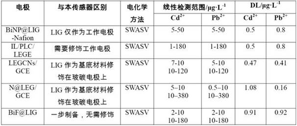
(七)LIG传感器的抗干扰、弯曲性能和再现性分析(7) Anti-interference, bending performance and reproducibility analysis of LIG sensor
在实际水样检测中非目标离子常与Cd 2+ 和 Pb 2+共存,极有可能对检测信号造成影响。因此,我们选择了七种常见的重金属离子对传感器的抗干扰性能进行了测试。SWASV测试是通过在含有20 μg·L-1 Cd2+和Pb2+的缓冲液中分别加入20倍目标离子浓度(400 μg•L-1)的Al3+、Cr2+、Cu2+、Hg2+、Mg2+、Mn2+、Zn2+进行了SWASV测试。图14中A图展示了空白干扰和每种干扰离子共存情况下Cd2+和Pb2+的峰值电流。结果表明,除Cu2+外其他干扰离子均未对信号产生很大干扰。在Cu2+离子存在时,Cd2+的检测信号为空白,Pb2+离子电流也明显减弱,这种变化的主要原因是Cu2+能够与目标离子竞争电极表面的活性位点。为解决实际检测中 Cu2+的干扰,可以通过加入0.1 mM的亚铁氰化钾形成稳定的不溶性Cu-亚铁氰化钾络合物的形式消除干扰。In actual water sample detection, non-target ions often coexist with Cd 2+ and Pb 2+ , which are very likely to affect the detection signal. Therefore, we selected seven common heavy metal ions to test the anti-interference performance of the sensor. The SWASV test was performed by adding Al 3+ , Cr 2+ ,
为测试传感器的柔性可弯曲性能,分别测试了在平面、凹面和凸面形状下(参见图16)的循环伏安图像,结果如图14中B图所示。凹面状态的CV曲线几乎与平面状态重合,而凸面状态电极的CV电流出现了较大的降低。这三种状态的CV曲线的Ipa、Ipc和ΔEp信息列于表4,与平面状态相比,凸面状态的Ipa和Ipc分别降低了25.90 μA 和22.60 μA,ΔEp增加了0.024 V。LIG 传感器在凹面状态下的Ipa、Ipc和ΔEp与平面状态下的几乎相同。为了探究不同状态下CV 曲线变化的原因,我们分别用数字万用表测试了凸凹弯曲过程从平坦状态的电阻变化,测试过程可以清楚地观察到随着凸面弯曲角度的增加其导线电阻逐渐增加,在弯曲角度约90°时电阻从280 Ω增加到约440 Ω,凹弯过程中并没有因角度的变化和平面阻力的变化而产生较大的变化。这种情况可能是由于碳化线与线材之间的连接区域因凸面弯曲而拉伸,减少了LIG之间的连接,从而增加了电阻。In order to test the flexibility and bendability of the sensor, the cyclic voltammetry images under the planar, concave and convex shapes (see Figure 16) were tested respectively, and the results are shown in Figure B in Figure 14. The CV curve of the concave state almost coincides with that of the planar state, while the CV current of the electrode in the convex state shows a larger decrease. The Ipa, Ipc, and ΔEp information of the CV curves of these three states are listed in Table 4. Compared with the planar state, the Ipa and Ipc of the convex state decreased by 25.90 μA and 22.60 μA, respectively, and the ΔEp increased by 0.024 V. The Ipa, Ipc and ΔEp of the LIG sensor in the concave state are almost the same as those in the planar state. In order to explore the reasons for the change of the CV curve in different states, we used a digital multimeter to test the resistance change from the flat state during the convex and concave bending process. During the test, it can be clearly observed that the wire resistance gradually increases with the increase of the convex bending angle. When the angle is about 90°, the resistance increases from 280 Ω to about 440 Ω. During the concave bending process, there is no major change due to the change of the angle and the change of the plane resistance. This situation may be due to the stretching of the connection area between the carbonized wire and the wire due to convex bending, reducing the connection between the LIGs and thus increasing the electrical resistance.
表4:不同柔性状态下LIG传感器的CV曲线的Ipa、Ipc和ΔEp信息Table 4: Ipa, Ipc and ΔEp information of CV curves of LIG sensors in different flexible states

用9根LIG电极测试含有20 μg·L-1 Cd2+和Pb2+的缓冲液,如图14中C图所示,展示了每根电极Cd2+和Pb2+的测试电流以及电极的平均电流。测试结果显示,Cd2+电流的RSD=5.6%,Pb2+电流的RSD=7.65%,这表明制备的传感器具备良好的再现性。The buffer solution containing 20 μg·L -1 Cd 2+ and Pb 2+ was tested with 9 LIG electrodes, as shown in Figure C in Figure 14, showing the test current of each electrode Cd 2+ and Pb 2+ and the electrodes the average current. The test results show that the RSD of the Cd 2+ current is 5.6%, and the RSD of the Pb 2+ current is 7.65%, which indicates that the fabricated sensor has good reproducibility.
(八)LIG传感器的实际水样测试(8) Actual water sample test of LIG sensor
如表5所示,对自来水中Cd2+和Pb2+的加标回收实验结果,我们分别通过SWASV和等离子体质谱仪(ICPMS)分析了低加标浓度(10 μg·L-1 、20 μg·L-1)和高加标浓度(60 μg·L-1)的结果,并测量了Cd2+和Pb2+的加标回收率在85.40%-109.46%范围内。两种方法测得的结果相近,证明LIG集成电极可以满足真实水样的检测需求。As shown in Table 5, the experimental results of the spiked recovery of Cd 2+ and Pb 2+ in tap water were analyzed by SWASV and plasma mass spectrometer (ICPMS) at low spiked concentrations (10 μg·L -1 , 20 μg·L -1 , 20 μg·L -1 ) and high spiked concentration (60 μg·L -1 ), and the spiked recoveries of Cd 2+ and Pb 2+ were measured in the range of 85.40%-109.46%. The results obtained by the two methods are similar, which proves that the LIG integrated electrode can meet the detection requirements of real water samples.
表5:自来水中 Cd 2+ 和 Pb 2+的加标回收实验结果Table 5: Experimental results of spiked recovery of Cd 2+ and Pb 2+ in tap water

结论in conclusion
通过激光划线直接将LIG集成电极直接印刷在PI薄膜表面,对不同激光功率、划线间距和划线速度下制备的LIG进行表征分析,阐明了影响规律,最终确定了最佳激光参数并对Cd2+和Pb2+的SWASV检测条件和环境进行了优化。LIG集成电极具有优异的抗干扰性、重现性和柔性的检测性能,已成功用于真实水样中HMIs的检测。LIG集成电极不仅制造简单,而且无需额外修饰材料即可用于人机界面检测,整个过程不需要剧毒试剂。该研究为柔性传感器在人机界面检测中的应用提供了新的前景。The LIG integrated electrodes were directly printed on the surface of the PI film by laser scribing. The LIGs prepared under different laser power, scribing spacing and scribing speed were characterized and analyzed, the influence laws were clarified, and the optimal laser parameters were finally determined. The SWASV detection conditions and environment for Cd 2+ and Pb 2+ were optimized. The LIG integrated electrode has excellent anti-interference, reproducibility and flexible detection performance, and has been successfully used in the detection of HMIs in real water samples. The LIG integrated electrode is not only simple to manufacture, but also can be used for human-machine interface detection without additional modification materials, and the whole process does not require highly toxic reagents. This study provides a new prospect for the application of flexible sensors in human-machine interface detection.
以上内容是结合具体的实施方式对本发明所作的进一步详细说明,不能认定本发明的具体实施只局限于这些说明。对于本发明所属技术领域的普通技术人员来说,在不脱离本发明构思的前提下,还可以做出若干简单推演或替换。The above content is a further detailed description of the present invention in conjunction with specific embodiments, and it cannot be considered that the specific implementation of the present invention is limited to these descriptions. For those skilled in the art to which the present invention pertains, some simple deductions or substitutions can be made without departing from the concept of the present invention.
Claims (10)
Priority Applications (1)
| Application Number | Priority Date | Filing Date | Title |
|---|---|---|---|
| CN202210943951.7A CN115015345B (en) | 2022-08-08 | 2022-08-08 | Non-modified flexible electrochemical sensor for rapidly detecting heavy metal ions and preparation method and application thereof |
Applications Claiming Priority (1)
| Application Number | Priority Date | Filing Date | Title |
|---|---|---|---|
| CN202210943951.7A CN115015345B (en) | 2022-08-08 | 2022-08-08 | Non-modified flexible electrochemical sensor for rapidly detecting heavy metal ions and preparation method and application thereof |
Publications (2)
| Publication Number | Publication Date |
|---|---|
| CN115015345A true CN115015345A (en) | 2022-09-06 |
| CN115015345B CN115015345B (en) | 2022-10-28 |
Family
ID=83066193
Family Applications (1)
| Application Number | Title | Priority Date | Filing Date |
|---|---|---|---|
| CN202210943951.7A Active CN115015345B (en) | 2022-08-08 | 2022-08-08 | Non-modified flexible electrochemical sensor for rapidly detecting heavy metal ions and preparation method and application thereof |
Country Status (1)
| Country | Link |
|---|---|
| CN (1) | CN115015345B (en) |
Cited By (4)
| Publication number | Priority date | Publication date | Assignee | Title |
|---|---|---|---|---|
| CN115452908A (en) * | 2022-09-22 | 2022-12-09 | 闽江学院 | A kind of preparation method and application of graphene microelectrode based on smart phone detection |
| CN116593553A (en) * | 2023-04-28 | 2023-08-15 | 中国地质大学(北京) | A graphene electrode for detecting chromium (VI) ions in water environment and its application |
| CN116858911A (en) * | 2023-06-07 | 2023-10-10 | 复旦大学 | Sweat sensing patch and preparation method thereof |
| EP4635912A1 (en) * | 2024-04-16 | 2025-10-22 | Scuola Superiore Sant'Anna di Pisa | Method of scribing laser-induced graphene |
Citations (11)
| Publication number | Priority date | Publication date | Assignee | Title |
|---|---|---|---|---|
| CN110560910A (en) * | 2019-08-21 | 2019-12-13 | 武汉大学 | Laser engraving preparation method of low-background graphene electrode array and electrochemical sensor preparation method |
| US20200150075A1 (en) * | 2016-07-21 | 2020-05-14 | King Abdullah University Of Science And Technology | On-chip graphene electrode, methods of making, and methods of use |
| CN112611794A (en) * | 2020-12-14 | 2021-04-06 | 南京农业大学 | Batch preparation method of heavy metal ion electrochemical sensors |
| CN112723855A (en) * | 2019-10-14 | 2021-04-30 | 武汉大学 | Laser engraving preparation method and application of graphene-ceramic composite electrode array |
| CN112903768A (en) * | 2021-01-21 | 2021-06-04 | 江苏集萃微纳自动化系统与装备技术研究所有限公司 | Preparation method of electrochemical immunosensor based on laser-induced graphene |
| US20210215636A1 (en) * | 2020-01-14 | 2021-07-15 | Iowa State University Research Foundation, Inc. | Aerosol jet printed flexible graphene circuits for electrochemical sensing and biosensing |
| CN113295748A (en) * | 2021-05-21 | 2021-08-24 | 闽江学院 | Preparation of laser direct-writing graphene/precious metal nanoparticle composite electrode and application of immunosensing |
| CN113311044A (en) * | 2021-06-19 | 2021-08-27 | 中国地质大学(北京) | Sensor capable of rapidly detecting nitrite in water environment and detection method |
| CN113325053A (en) * | 2021-06-08 | 2021-08-31 | 中国地质大学(北京) | Cadmium ion electrochemical sensor working electrode and preparation method, detection method and application thereof |
| US20210332489A1 (en) * | 2020-04-27 | 2021-10-28 | Iowa State University Research Foundation, Inc. | Laser-induced graphene electrodes adaptable for electrochemical sensing and catalysis |
| CN114705736A (en) * | 2022-03-21 | 2022-07-05 | 山东大学 | Portable multi-channel detection electrochemical sensing system and application thereof |
-
2022
- 2022-08-08 CN CN202210943951.7A patent/CN115015345B/en active Active
Patent Citations (11)
| Publication number | Priority date | Publication date | Assignee | Title |
|---|---|---|---|---|
| US20200150075A1 (en) * | 2016-07-21 | 2020-05-14 | King Abdullah University Of Science And Technology | On-chip graphene electrode, methods of making, and methods of use |
| CN110560910A (en) * | 2019-08-21 | 2019-12-13 | 武汉大学 | Laser engraving preparation method of low-background graphene electrode array and electrochemical sensor preparation method |
| CN112723855A (en) * | 2019-10-14 | 2021-04-30 | 武汉大学 | Laser engraving preparation method and application of graphene-ceramic composite electrode array |
| US20210215636A1 (en) * | 2020-01-14 | 2021-07-15 | Iowa State University Research Foundation, Inc. | Aerosol jet printed flexible graphene circuits for electrochemical sensing and biosensing |
| US20210332489A1 (en) * | 2020-04-27 | 2021-10-28 | Iowa State University Research Foundation, Inc. | Laser-induced graphene electrodes adaptable for electrochemical sensing and catalysis |
| CN112611794A (en) * | 2020-12-14 | 2021-04-06 | 南京农业大学 | Batch preparation method of heavy metal ion electrochemical sensors |
| CN112903768A (en) * | 2021-01-21 | 2021-06-04 | 江苏集萃微纳自动化系统与装备技术研究所有限公司 | Preparation method of electrochemical immunosensor based on laser-induced graphene |
| CN113295748A (en) * | 2021-05-21 | 2021-08-24 | 闽江学院 | Preparation of laser direct-writing graphene/precious metal nanoparticle composite electrode and application of immunosensing |
| CN113325053A (en) * | 2021-06-08 | 2021-08-31 | 中国地质大学(北京) | Cadmium ion electrochemical sensor working electrode and preparation method, detection method and application thereof |
| CN113311044A (en) * | 2021-06-19 | 2021-08-27 | 中国地质大学(北京) | Sensor capable of rapidly detecting nitrite in water environment and detection method |
| CN114705736A (en) * | 2022-03-21 | 2022-07-05 | 山东大学 | Portable multi-channel detection electrochemical sensing system and application thereof |
Non-Patent Citations (1)
| Title |
|---|
| SEONG-EUN JEONG ET AL.: ""Simple laser-induced graphene fiber electrode fabrication for high-performance heavy-metal sensing"", 《MICROCHEMICAL JOURNAL》 * |
Cited By (5)
| Publication number | Priority date | Publication date | Assignee | Title |
|---|---|---|---|---|
| CN115452908A (en) * | 2022-09-22 | 2022-12-09 | 闽江学院 | A kind of preparation method and application of graphene microelectrode based on smart phone detection |
| CN116593553A (en) * | 2023-04-28 | 2023-08-15 | 中国地质大学(北京) | A graphene electrode for detecting chromium (VI) ions in water environment and its application |
| CN116593553B (en) * | 2023-04-28 | 2025-12-02 | 中国地质大学(北京) | A graphene electrode for detecting chromium (VI) ions in an aquatic environment and its application. |
| CN116858911A (en) * | 2023-06-07 | 2023-10-10 | 复旦大学 | Sweat sensing patch and preparation method thereof |
| EP4635912A1 (en) * | 2024-04-16 | 2025-10-22 | Scuola Superiore Sant'Anna di Pisa | Method of scribing laser-induced graphene |
Also Published As
| Publication number | Publication date |
|---|---|
| CN115015345B (en) | 2022-10-28 |
Similar Documents
| Publication | Publication Date | Title |
|---|---|---|
| CN115015345B (en) | Non-modified flexible electrochemical sensor for rapidly detecting heavy metal ions and preparation method and application thereof | |
| Zhu et al. | Disposable and portable gold nanoparticles modified-laser-scribed graphene sensing strips for electrochemical, non-enzymatic detection of glucose | |
| Nagaraju et al. | Hierarchical Ni–Co layered double hydroxide nanosheets entrapped on conductive textile fibers: a cost-effective and flexible electrode for high-performance pseudocapacitors | |
| Thanh et al. | In situ synthesis of graphene-encapsulated gold nanoparticle hybrid electrodes for non-enzymatic glucose sensing | |
| JP2011174184A5 (en) | ||
| CN103931034B (en) | Current collector plate for fuel cell and manufacturing method thereof | |
| KR101816800B1 (en) | Method of preparing metal nano wire and 3D metal nano catalyst | |
| Lee et al. | Porous fluorine-doped tin oxide as a promising substrate for electrochemical biosensors—demonstration in hydrogen peroxide sensing | |
| CN108226138A (en) | A kind of hollow pipe array surface enhancing Raman scattering substrate of Ag nanometer sheets assembling | |
| Bommineedi et al. | Screen printing: an ease thin film technique | |
| CN112630274A (en) | Nano-porous silver electrode for simultaneously detecting acetaminophen and dopamine, and preparation method and application thereof | |
| Hsieh et al. | Synthesis of silver nanoparticles on carbon papers for electrochemical catalysts | |
| CN107937957A (en) | The preparation method of surface enhanced Raman substrate and the substrate are used to detect animal virus | |
| CN101165213B (en) | Preparation method of self-assembled gold nanorod array electrode after dispersion | |
| CN103194751B (en) | Nickel nanorod-nickel oxide nanosheet hierarchical structure array modified with silver nanoparticles and preparation method and application thereof | |
| Karczmarczyk et al. | Electrocatalytic glucose oxidation at gold and gold-carbon nanoparticulate film prepared from oppositely charged nanoparticles | |
| CN113030209B (en) | Method for preparing flexible graphene electrode in rapid and controllable manner and application | |
| CN101165214B (en) | A preparation method of nanorod array electrode modified after dispersion | |
| CN106672897A (en) | Array type silver nano-pillar coated with gold film at its surface and preparation method thereof | |
| TW202035720A (en) | Porous copper composite and mehtod thereof | |
| CN101493433A (en) | Gold plated ZnO nano-bar array electrode and method for making same | |
| CN105112913B (en) | A kind of transferable Fe2O3/ Au nano-pore array thin films and preparation method thereof | |
| JP2025502121A (en) | Process for Producing Anodes for Lithium Batteries | |
| CN103757675B (en) | A kind of fine and close gold thin film method of AFM silicon needle point pulse plating nano thickness | |
| CN109560148A (en) | A kind of nano generator and preparation method based on nano structure membrane electrode |
Legal Events
| Date | Code | Title | Description |
|---|---|---|---|
| PB01 | Publication | ||
| PB01 | Publication | ||
| SE01 | Entry into force of request for substantive examination | ||
| SE01 | Entry into force of request for substantive examination | ||
| GR01 | Patent grant | ||
| GR01 | Patent grant |