CN114883169A - Electrode fixing assembly and dry etching equipment - Google Patents
Electrode fixing assembly and dry etching equipment Download PDFInfo
- Publication number
- CN114883169A CN114883169A CN202210520435.3A CN202210520435A CN114883169A CN 114883169 A CN114883169 A CN 114883169A CN 202210520435 A CN202210520435 A CN 202210520435A CN 114883169 A CN114883169 A CN 114883169A
- Authority
- CN
- China
- Prior art keywords
- fixing member
- mounting hole
- electrode
- fixing
- alloy
- Prior art date
- Legal status (The legal status is an assumption and is not a legal conclusion. Google has not performed a legal analysis and makes no representation as to the accuracy of the status listed.)
- Pending
Links
Images


Classifications
-
- H10P72/0421—
-
- H—ELECTRICITY
- H01—ELECTRIC ELEMENTS
- H01J—ELECTRIC DISCHARGE TUBES OR DISCHARGE LAMPS
- H01J37/00—Discharge tubes with provision for introducing objects or material to be exposed to the discharge, e.g. for the purpose of examination or processing thereof
- H01J37/32—Gas-filled discharge tubes
- H01J37/32431—Constructional details of the reactor
- H01J37/32458—Vessel
- H01J37/32477—Vessel characterised by the means for protecting vessels or internal parts, e.g. coatings
-
- H—ELECTRICITY
- H01—ELECTRIC ELEMENTS
- H01J—ELECTRIC DISCHARGE TUBES OR DISCHARGE LAMPS
- H01J37/00—Discharge tubes with provision for introducing objects or material to be exposed to the discharge, e.g. for the purpose of examination or processing thereof
- H01J37/32—Gas-filled discharge tubes
- H01J37/32431—Constructional details of the reactor
- H01J37/32532—Electrodes
- H01J37/3255—Material
-
- H—ELECTRICITY
- H01—ELECTRIC ELEMENTS
- H01J—ELECTRIC DISCHARGE TUBES OR DISCHARGE LAMPS
- H01J37/00—Discharge tubes with provision for introducing objects or material to be exposed to the discharge, e.g. for the purpose of examination or processing thereof
- H01J37/32—Gas-filled discharge tubes
- H01J37/32431—Constructional details of the reactor
- H01J37/32532—Electrodes
- H01J37/32559—Protection means, e.g. coatings
-
- H—ELECTRICITY
- H01—ELECTRIC ELEMENTS
- H01J—ELECTRIC DISCHARGE TUBES OR DISCHARGE LAMPS
- H01J37/00—Discharge tubes with provision for introducing objects or material to be exposed to the discharge, e.g. for the purpose of examination or processing thereof
- H01J37/32—Gas-filled discharge tubes
- H01J37/32431—Constructional details of the reactor
- H01J37/32532—Electrodes
- H01J37/32568—Relative arrangement or disposition of electrodes; moving means
-
- H—ELECTRICITY
- H01—ELECTRIC ELEMENTS
- H01J—ELECTRIC DISCHARGE TUBES OR DISCHARGE LAMPS
- H01J37/00—Discharge tubes with provision for introducing objects or material to be exposed to the discharge, e.g. for the purpose of examination or processing thereof
- H01J37/32—Gas-filled discharge tubes
- H01J37/32431—Constructional details of the reactor
- H01J37/32715—Workpiece holder
-
- H—ELECTRICITY
- H01—ELECTRIC ELEMENTS
- H01J—ELECTRIC DISCHARGE TUBES OR DISCHARGE LAMPS
- H01J2237/00—Discharge tubes exposing object to beam, e.g. for analysis treatment, etching, imaging
- H01J2237/03—Mounting, supporting, spacing or insulating electrodes
- H01J2237/032—Mounting or supporting
-
- H—ELECTRICITY
- H01—ELECTRIC ELEMENTS
- H01J—ELECTRIC DISCHARGE TUBES OR DISCHARGE LAMPS
- H01J2237/00—Discharge tubes exposing object to beam, e.g. for analysis treatment, etching, imaging
- H01J2237/32—Processing objects by plasma generation
- H01J2237/33—Processing objects by plasma generation characterised by the type of processing
- H01J2237/334—Etching
Landscapes
- Physics & Mathematics (AREA)
- Engineering & Computer Science (AREA)
- Plasma & Fusion (AREA)
- Chemical & Material Sciences (AREA)
- Analytical Chemistry (AREA)
- Drying Of Semiconductors (AREA)
Abstract
The embodiment of the application provides an electrode fixing assembly and dry etching equipment. The electrode fixing assembly comprises a first fixing piece and a second fixing piece, wherein the hardness of the material of the first fixing piece is greater than that of the material of the second fixing piece; the electrode fixing assembly is used for being arranged in the dry etching equipment to fix the upper electrode on the equipment body, the first fixing piece and the second fixing piece are both arranged between the upper electrode and the equipment body, one side, far away from the second fixing piece, of the first fixing piece is arranged towards the equipment body, and one side, far away from the first fixing piece, of the second fixing piece is arranged towards the upper electrode. When the electrode fixing component rubs with the equipment body, the surface of the electrode fixing component is not easily abraded, so that the generation of particles can be reduced or eliminated, the problems that the etching is poor due to the fact that the substrate to be etched is covered by the particles and the like are avoided, the product yield is improved, and the production cost is reduced.
Description
Technical Field
The application relates to the technical field of etching, in particular to an electrode fixing assembly and dry etching equipment.
Background
In the field of display technology, a substrate is usually etched by a dry etching process to produce a corresponding pattern (pattern), specifically, the substrate to be etched is placed in a dry etching device, and a material to be etched on the substrate is removed by plasma discharge to perform etching.
The dry etching equipment mainly comprises: the device comprises a device body, an upper electrode and a lower electrode which are positioned in a reaction cavity of the device body, and a base platform which is positioned on the lower electrode and used for placing a substrate; when the method is specifically implemented, a substrate to be etched is placed on a base platform above a lower electrode, plasma gas is introduced into a reaction cavity, the reaction cavity is sealed, and voltage is applied to an upper electrode and the lower electrode to form a potential difference between the upper electrode and the lower electrode, so that the plasma is driven to move towards the substrate to etch the substrate.
In the dry etching equipment, an electrode fixing seat is usually arranged between an equipment body and an upper electrode, and when the upper electrode, the electrode fixing seat and the equipment body are fixedly connected, the upper electrode can be fixed on the equipment body; however, in the conventional dry etching apparatus, when friction occurs between the electrode holder and the apparatus body, the surface of the electrode holder is easily abraded to generate particles (particles), the particles may contaminate the environment in the reaction chamber, and when the particles fall onto the substrate, the portion of the substrate covered by the particles cannot be etched by the plasma, so that poor etching occurs, the yield of the product is reduced, and the production cost is increased.
Disclosure of Invention
The embodiment of the application provides an electrode fixing component and dry etching equipment, when taking place the friction between this electrode fixing component and the equipment body, the surface of electrode fixing component is difficult to by wearing and tearing to can reduce or eliminate the production of particulate matter, and then avoid treating the etching base plate because the etching scheduling problem that is covered by the particulate matter and leads to can improve the product yield and reduction in production cost.
In a first aspect, an embodiment of the present application provides an electrode fixing assembly, including a first fixing member and a second fixing member, wherein a hardness of a material of the first fixing member is greater than a hardness of a material of the second fixing member;
the electrode fixing assembly is used for being arranged in dry etching equipment to fix an upper electrode on an equipment body, the first fixing piece and the second fixing piece are arranged between the upper electrode and the equipment body, one side, far away from the second fixing piece, of the first fixing piece faces the equipment body, and one side, far away from the first fixing piece, of the second fixing piece faces the upper electrode.
In some embodiments, the material of the second fixing member includes aluminum, and the material of the first fixing member includes a metal material having hardness greater than that of aluminum.
In some embodiments, the material of the first securing member includes at least one of iron, an iron alloy, tungsten, a tungsten alloy, vanadium, a vanadium alloy, manganese, a manganese alloy, iridium, an iridium alloy, molybdenum, a molybdenum alloy, cobalt, a cobalt alloy, zirconium, a zirconium alloy, beryllium, a beryllium alloy, titanium, a titanium alloy, chromium, a chromium alloy, tantalum, a tantalum alloy, nickel, a nickel alloy, niobium, and a niobium alloy.
In some embodiments, the ratio of the thickness of the first fixing part to the thickness of the second fixing part is (1-5): 8-12.
In some embodiments, a first mounting hole is formed in the first fixing member, a second mounting hole is formed in the second fixing member, and the first mounting hole and the second mounting hole are correspondingly formed; and/or
The first fixing piece is provided with a fourth mounting hole, the second fixing piece is provided with a fifth mounting hole, and the fourth mounting hole and the fifth mounting hole are correspondingly arranged.
In some embodiments, the outer surface of the second fixing member is provided with a protective layer.
In some embodiments, the material of the protective layer comprises yttria.
In a second aspect, an embodiment of the present application provides a dry etching apparatus, including:
an apparatus body having an inner cavity;
the upper electrode is arranged in the inner cavity of the equipment body;
the electrode fixing assembly is arranged in an inner cavity of the equipment body, the upper electrode, the electrode fixing assembly and the equipment body are connected, and the first fixing piece and the second fixing piece are arranged between the upper electrode and the equipment body, wherein one side of the first fixing piece, which is far away from the second fixing piece, is arranged towards the equipment body, and one side of the second fixing piece, which is far away from the first fixing piece, is arranged towards the upper electrode;
and the lower electrode is arranged in the inner cavity of the equipment body, and the lower electrode and the upper electrode are oppositely arranged.
In some embodiments, a first mounting hole is formed in the first fixing member, a second mounting hole is formed in the second fixing member, a third mounting hole is formed in the apparatus body, the first mounting hole, the second mounting hole and the third mounting hole are correspondingly arranged, and the first fixing member, the second fixing member and the apparatus body are fixedly connected through a first fastener penetrating through the first mounting hole, the second mounting hole and the third mounting hole; and/or
The electrode fixing device is characterized in that a fourth mounting hole is formed in the first fixing piece, a fifth mounting hole is formed in the second fixing piece, a sixth mounting hole is formed in the upper electrode, the fourth mounting hole, the fifth mounting hole and the sixth mounting hole are correspondingly arranged, and the first fixing piece, the second fixing piece and the upper electrode are fixedly connected through a second fastener penetrating through the fourth mounting hole, the fifth mounting hole and the sixth mounting hole.
The electrode fixing assembly provided by the embodiment of the application can replace a traditional electrode fixing seat to be applied to dry etching equipment, and is used for fixing an upper electrode on an equipment body, the hardness of the material of the first fixing piece in the electrode fixing assembly is larger than that of the material of the second fixing piece, and the first fixing piece is arranged towards the equipment body, namely, the part with the larger hardness in the electrode fixing assembly is arranged to be in contact with the equipment body, the hardness of the material of the first fixing piece is larger, the wear resistance is better, when friction occurs between the first fixing piece and the equipment body, the surface of the first fixing piece is not easily abraded, so that the generation of particles is reduced or eliminated, the problems that the substrate to be etched is poor in etching due to the fact that the substrate is covered by the particles can be avoided, the product yield is improved, and the production cost is reduced.
Drawings
In order to more clearly illustrate the technical solutions in the embodiments of the present application, the drawings used in the description of the embodiments will be briefly described below. It is obvious that the drawings in the following description are only some embodiments of the application, and that for a person skilled in the art, other drawings can be derived from them without inventive effort.
Fig. 1 is a schematic side view of an electrode fixing assembly according to an embodiment of the present disclosure.
Fig. 2 is a schematic top view of a first fixing element according to an embodiment of the present disclosure.
Fig. 3 is a schematic cross-sectional view of the first fixing member of fig. 2 along the direction a-a.
Fig. 4 is a schematic top view of a second fixing element according to an embodiment of the present disclosure.
Fig. 5 is a schematic cross-sectional view of the second fixing member of fig. 4 taken along the direction B-B.
Fig. 6 is a schematic cross-sectional view of an electrode fixing assembly provided in an embodiment of the present application.
Fig. 7 is a schematic structural diagram of a dry etching apparatus provided in an embodiment of the present application.
Detailed Description
The technical solution in the embodiments of the present application will be clearly and completely described below with reference to the drawings in the embodiments of the present application. It is to be understood that the embodiments described are only a few embodiments of the present application and not all embodiments. All other embodiments, which can be derived by a person skilled in the art from the embodiments given herein without making any creative effort, shall fall within the protection scope of the present application.
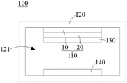
Referring to fig. 1, fig. 1 is a schematic side view of an electrode fixing assembly according to an embodiment of the present disclosure. The embodiment of the present application provides an electrode fixing assembly 110, which includes a first fixing member 10 and a second fixing member 20, wherein the hardness of the material of the first fixing member 10 is greater than that of the material of the second fixing member 20.
The electrode fixing assembly 110 is configured to be disposed in a dry etching apparatus to fix an upper electrode on an apparatus body 120, and a first fixing member 10 and a second fixing member 20 are disposed between the upper electrode 130 and the apparatus body 120, wherein a side of the first fixing member 10 away from the second fixing member 20 is disposed toward the apparatus body, and a side of the second fixing member 20 away from the first fixing member 10 is disposed toward the upper electrode.
The electrode fixing assembly 110 provided by the embodiment of the present application can be applied to a dry etching apparatus instead of a conventional electrode fixing base, and is used for fixing an upper electrode on the apparatus body 120, since the hardness of the material of the first fixing member 10 is greater than that of the material of the second fixing member 20 in the electrode fixing assembly 110, and the first fixing member 10 is disposed toward the apparatus body, that is, the member having the greater hardness in the electrode fixing assembly 110 is disposed to be in contact with the apparatus body, since the hardness of the material of the first fixing member 10 is high, and the wear resistance is good, when friction occurs between the first fixing member 10 and the apparatus body, the surface of the first fixing member 10 is not easily abraded, thereby reducing or eliminating the generation of particles, therefore, the problems of poor etching and the like caused by the fact that the substrate to be etched is covered by particles can be avoided, the product yield is improved, and the production cost is reduced.
Illustratively, the material of the second fixing member 20 includes aluminum (Al), and the material of the first fixing member 10 includes a metal material having a hardness greater than that of aluminum.
Illustratively, the material of the first fixing member 10 includes at least one of iron (Fe), iron alloy, tungsten (W), tungsten alloy, vanadium (V), vanadium alloy, manganese (Mn), manganese alloy, iridium (Ir), iridium alloy, molybdenum (Mo), molybdenum alloy, cobalt (Co), cobalt alloy, zirconium (Zr), zirconium alloy, beryllium (Be), beryllium alloy, titanium (Ti), titanium alloy, chromium (Cr), chromium alloy, tantalum (Ta), tantalum alloy, nickel (Ni), nickel alloy, niobium (Nb), and niobium alloy.
In some embodiments, the material of the first fixing member 10 may be an iron alloy, such as stainless steel, wherein SUS316 stainless steel has the advantages of high hardness, wear resistance, corrosion resistance, etc., and thus the wear resistance of the first fixing member 10 can be significantly improved, and the generation of particles when friction occurs between the first fixing member 10 and the apparatus body 120 can be prevented.
Illustratively, the ratio of the thickness W1 of the first fastener piece 10 to the thickness W2 of the second fastener piece 20 may be (1-5) to (8-12), such as 1:10, 2:10, 3:10, 4:10, 5:10, 3:8, 3:9, 3:11, 3:12, 1: 8. 1: 12. 5: 8. 5: 12, etc. It can be understood that since the material of the first mount 10 has a relatively high cost and the material of the second mount 20 has a relatively low cost, by setting the thickness W1 of the first mount 10 to a small thickness and setting the thickness of the material of the second mount 20 to a large thickness, it is possible to reduce the production cost to the maximum extent while ensuring good mechanical strength of the electrode fixing assembly 110.
Illustratively, the thickness W1 of the first attachment member 10 is 1mm to 5mm, such as 1mm, 2mm, 3mm, 4mm, 5mm, and the like.
Illustratively, the thickness W2 of the second attachment member 20 is 8mm to 12mm, such as 8mm, 9mm, 10mm, 11mm, 12mm, and the like.
In some embodiments, the thickness W1 of the first mount 10 is 3mm, and the thickness W2 of the second mount 20 is 10mm, i.e., the total thickness of the electrode mount assembly 110 is 13 mm.
Illustratively, the outer surface of the second fixing member 20 is provided with a protective layer (not shown). Illustratively, the material of the second fixing member 20 may include a metal material such as aluminum, and when the second fixing member 20 is an aluminum material, the aluminum material may be anodized to form an oxide film, that is, the second fixing member 20 includes an aluminum material and an oxide film (aluminum oxide) on an outer surface of the aluminum material. Because the aluminum material or the oxide film is easy to be mixed with the process gas (NF) 3 ) The reaction results in the second fixed part 20 being corroded to generate particles, and the particles can also generate problems of poor etching and the like when falling on a substrate to be etched, so that the protective layer is arranged on the outer surface of the second fixed part 20, and the effect of preventing the particles from being generated due to the corrosion of the second fixed part 20 can be achieved.
Illustratively, the material of the protective layer includes yttria (Y) 2 O 3 ) Since yttria is chemically stable, it does not react with process gases (e.g., NF) 3 Etc.), so that the second fixing member 20 can be effectively protected, the generation of particles caused by corrosion of the second fixing member 20 is avoided, and the occurrence of problems such as poor etching is further reduced.
It should be noted that, in the conventional dry etching apparatus, the electrode holder for fixing the upper electrode is usually made of aluminum material, the aluminum material is not only prone to generate particles (the first source of the particles) due to friction with the apparatus body, but also prone to generate process gas (such as NF) on the outer surface of the aluminum material 3 Etc.) to cause a reaction that results in the production of particulates (a second source of particulates). The embodiment of the present application is constructed by replacing the conventional electrode holder with the electrode holder assembly 110 including the first holder 10 and the second holder 20, since the part of the electrode fixing assembly 110 that contacts the apparatus body is the first fixing member 10, and the hardness of the material of the first fixing piece 10 is relatively high, and the abrasion resistance is relatively good, so when friction occurs between the first fixing piece 10 and the equipment body, the surface of the first fixing piece 10 is not easily abraded, thereby eliminating the first source of particles, and in addition, the embodiment of the present application can effectively protect the second fixing member 20 by providing the protective layer on the outer surface of the second fixing member 20, prevent the outer surface of the second fixing member 20 from being corroded to cause particles, therefore, the second source of the particles is eliminated, that is, the embodiment of the application eliminates or reduces the generation of the particles through two ways, thereby eliminating or reducing the occurrence of poor etching and the like.
Referring to fig. 2 to 6, a first mounting hole 11 is formed in the first fixing member 10, a second mounting hole 22 is formed in the second fixing member 20, a third mounting hole may be formed in the apparatus body, the first mounting hole 11, the second mounting hole 22 and the third mounting hole are correspondingly formed, and the first fixing member 10, the second fixing member 20 and the apparatus body are fixedly connected through a first fastening member penetrating through the first mounting hole 11, the second mounting hole 22 and the third mounting hole, so that the electrode fixing assembly 110 and the apparatus body of the dry etching apparatus are fixedly connected.
Illustratively, the first fastener may be a screw; in some embodiments, the hole walls of the third installation hole on the equipment body, the first installation hole 11 on the first fixing piece 10 and the second installation hole 22 on the second fixing piece 20 may be provided with internal threads, and when the equipment body, the first fixing piece 10 and the second fixing piece 20 are sequentially arranged, the internal threads on the hole walls of the third installation hole, the first installation hole 11 and the second installation hole 22 are in a continuous state and matched with the external threads of the screw; in other embodiments, the hole wall of the third mounting hole on the device body is not provided with an internal thread and is a smooth hole, and the hole walls of the first mounting hole 11 and the second mounting hole 22 are provided with an internal thread and are in a continuous state and matched with the external thread of the screw; in other embodiments, the third mounting hole on the device body and the hole wall of the first mounting hole 11 on the first fixing member 10 may not be provided with internal threads, and both are smooth holes, and the hole wall of the second mounting hole 22 on the second fixing member 20 is provided with internal threads and matches with the external threads of the screw.
Referring to fig. 2 to 6, the first fixing member 10 is further provided with a fourth mounting hole 14, the second fixing member 20 is further provided with a fifth mounting hole 25, the upper electrode may be provided with a sixth mounting hole, the fourth mounting hole 14, the fifth mounting hole 25 and the sixth mounting hole are correspondingly arranged, and the first fixing member 10, the second fixing member 20 and the upper electrode are fixedly connected through a second fastening member penetrating through the fourth mounting hole 14, the fifth mounting hole 25 and the sixth mounting hole, so that the electrode fixing assembly 110 is fixedly connected with the upper electrode.
Referring to fig. 3, the fourth mounting hole 14 may include a first via hole 141 and a second via hole 142 that are mutually penetrated, wherein the aperture of the first via hole 141 is larger than that of the second via hole 142, and the aperture of the second via hole 142 is the same as that of the fifth mounting hole 25 and that of the sixth mounting hole. When the second fastening member is a screw, the head of the screw may be received in the first through hole 141, and the threaded portion of the screw may pass through the second through hole 142, the fifth mounting hole 25 and the sixth mounting hole to fix the first fixing member 10, the second fixing member 20 and the upper electrode 130, and since the head of the screw may be received in the first through hole 141, that is, the head of the screw does not protrude out of the outer surface of the electrode fixing assembly 110, the flatness of the outer surface of the electrode fixing assembly 110 may be maintained, so that the stability of the connection between the electrode fixing assembly 110 and the apparatus body of the dry etching apparatus may not be affected.
Referring to fig. 2, the first fixing member 10 may include a first transverse portion 101 and a first longitudinal portion 102 connected to each other, the first transverse portion 101 and the first longitudinal portion 102 are disposed in a crossing manner, for example, the first mounting hole 11 is disposed at an intersection of the first transverse portion 101 and the first longitudinal portion 102, both ends of the first transverse portion 101 may be provided with fourth mounting holes 14, both ends of the first longitudinal portion 102 may be provided with the fourth mounting holes 14, that is, the first fixing member 10 may be provided with four fourth mounting holes 14. Illustratively, the first transverse portion 101 and the first longitudinal portion 102 are perpendicular to each other. According to the embodiment of the present application, the fourth mounting holes 14 are formed at both ends of the first transverse portion 101 and both ends of the first longitudinal portion 102, that is, the fourth mounting holes 14 are formed at four top ends of the cross-shaped structure of the first fixing member 10, and since the fourth mounting holes 14 are used for realizing the fixed connection between the electrode fixing assembly 110 and the upper electrode, the connection stability between the electrode fixing assembly 110 and the upper electrode can be significantly improved.
Referring to fig. 4, the second fixing member 20 may include a second transverse portion 201 and a second longitudinal portion 202 connected to each other, the second transverse portion 201 and the second longitudinal portion 202 are arranged in an intersecting manner, for example, the second mounting hole 22 is arranged at an intersection of the second transverse portion 201 and the second longitudinal portion 202, both ends of the second transverse portion 201 may be provided with the fifth mounting holes 25, and both ends of the second longitudinal portion 202 may be provided with the fifth mounting holes 25, that is, four fifth mounting holes 25 may be arranged on the second fixing member 20. Illustratively, the second transverse portion 201 and the second longitudinal portion 202 are perpendicular to each other.
Referring to fig. 7, fig. 7 is a schematic structural diagram of a dry etching apparatus according to an embodiment of the present application. The embodiment of the present application further provides a dry etching apparatus 100, which includes an apparatus body 120, an upper electrode 130, and an electrode fixing assembly 110, where the electrode fixing assembly 110 may be the electrode fixing assembly 110 in any of the above embodiments.
The device body 120 has an inner cavity 121, the upper electrode 130 and the electrode fixing assembly 110 are both disposed in the inner cavity 121 of the device body 120, the upper electrode 130, the electrode fixing assembly 110 and the device body 120 are connected, the first fixing member 10 and the second fixing member 20 are disposed between the upper electrode 130 and the device body 120, wherein one side of the first fixing member 10 away from the second fixing member 20 is disposed toward the device body 120, and one side of the second fixing member 20 away from the first fixing member 10 is disposed toward the upper electrode 130.
Illustratively, the dry etching apparatus 100 may further include a lower electrode 140, and the lower electrode 140 is disposed in the inner cavity 121 of the apparatus body 120 and is disposed opposite to the upper electrode 130.
It can be understood that the dry etching apparatus 100 operates according to the following principle: a substrate to be etched is placed on the lower electrode 140, plasma gas is introduced into the inner cavity 121, and voltage is applied to the upper electrode 130 and the lower electrode 140, so that a potential difference is formed between the upper electrode 130 and the lower electrode 140, and the plasma is driven to move towards the substrate to etch the substrate. In the dry etching apparatus 100 according to the embodiment of the present application, particles are not easily generated on the surface of the electrode fixing assembly 110, so that the problems of poor etching and the like caused by the substrate to be etched being covered by the particles can be avoided, the yield of the product is improved, and the production cost is reduced.
Referring to fig. 2 to 7, a first mounting hole 11 is formed in the first fixing member 10, a second mounting hole 22 is formed in the second fixing member 20, a third mounting hole is formed in the device body 120, the first mounting hole 11, the second mounting hole 22 and the third mounting hole are correspondingly formed, and the first fixing member 10, the second fixing member 20 and the device body 120 are fixedly connected through a first fastening member penetrating through the first mounting hole 11, the second mounting hole 22 and the third mounting hole, so that the electrode fixing assembly 110 is fixedly connected with the device body 120 of the dry etching device 100. Illustratively, the first fastener may be a screw.
Referring to fig. 2 to 7, a fourth mounting hole 14 is further formed in the first fixing member 10, a fifth mounting hole 25 is further formed in the second fixing member 20, a sixth mounting hole is formed in the upper electrode 130, the fourth mounting hole 14, the fifth mounting hole 25 and the sixth mounting hole are correspondingly formed, and the first fixing member 10, the second fixing member 20 and the upper electrode 130 are fixedly connected by a second fastening member penetrating through the fourth mounting hole 14, the fifth mounting hole 25 and the sixth mounting hole, so that the electrode fixing assembly 110 and the upper electrode 130 are fixedly connected. Illustratively, the second fastener may be a screw.
Referring to fig. 3, the fourth mounting hole 14 includes a first via hole 141 and a second via hole 142 that are mutually penetrated, wherein the aperture of the first via hole 141 is larger than that of the second via hole 142, and the aperture of the second via hole 142 is the same as that of the fifth mounting hole 25 and that of the sixth mounting hole. When the second fastening member is a screw, the head of the screw may be received in the first through hole 141, and the threaded portion of the screw may pass through the second through hole 142, the fifth mounting hole 25 and the sixth mounting hole to fix the first fixing member 10, the second fixing member 20 and the upper electrode 130, and since the head of the screw may be received in the first through hole 141, that is, the head of the screw does not protrude out of the outer surface of the electrode fixing assembly 110, the flatness of the outer surface of the electrode fixing assembly 110 may be maintained, so that the stability of the connection between the electrode fixing assembly 110 and the apparatus body 120 of the dry etching apparatus 100 may not be affected.
For example, when the upper electrode 130 is mounted on the device body 120, the first fixing member 10, the second fixing member 20 and the upper electrode 130 may be fixedly connected by using the second fastening member, and then the first fixing member 10, the second fixing member 20 and the device body 120 may be fixedly connected by using the first fastening member.
Illustratively, the material of the second fixing member 20 includes aluminum (Al), and the material of the first fixing member 10 includes a metal material having a hardness greater than that of aluminum.
Illustratively, the material of the first fixing member 10 includes at least one of iron (Fe), iron alloy, tungsten (W), tungsten alloy, vanadium (V), vanadium alloy, manganese (Mn), manganese alloy, iridium (Ir), iridium alloy, molybdenum (Mo), molybdenum alloy, cobalt (Co), cobalt alloy, zirconium (Zr), zirconium alloy, beryllium (Be), beryllium alloy, titanium (Ti), titanium alloy, chromium (Cr), chromium alloy, tantalum (Ta), tantalum alloy, nickel (Ni), nickel alloy, niobium (Nb), and niobium alloy.
Illustratively, the ratio of the thickness W1 of the first fixing piece 10 to the thickness W2 of the second fixing piece 20 is (1-5): 8-12).
Illustratively, the outer surface of the second fixing member 20 is provided with a protective layer. Illustratively, the material of the second fixing member 20 may include a metal material such as aluminum, and when the second fixing member 20 is an aluminum material, the aluminum material may be anodized to form an oxide film, that is, the second fixing member 20 includes an aluminum material and an oxide film (aluminum oxide) provided on an outer surface of the aluminum material.
Illustratively, the material of the protective layer includes yttria (Y) 2 O 3 )。
The electrode fixing assembly and the dry etching apparatus provided in the embodiments of the present application are described in detail above. The principles and implementations of the present application are described herein using specific examples, which are presented only to aid in understanding the present application. Meanwhile, for those skilled in the art, according to the idea of the present application, there may be variations in the specific embodiments and the application scope, and in summary, the content of the present specification should not be construed as a limitation to the present application.
Claims (9)
Priority Applications (3)
| Application Number | Priority Date | Filing Date | Title |
|---|---|---|---|
| CN202210520435.3A CN114883169A (en) | 2022-05-12 | 2022-05-12 | Electrode fixing assembly and dry etching equipment |
| PCT/CN2022/094683 WO2023216318A1 (en) | 2022-05-12 | 2022-05-24 | Electrode fixing assembly and dry etching apparatus |
| US17/787,689 US20240186120A1 (en) | 2022-05-12 | 2022-05-24 | Electrode fixing assembly and dry etching device |
Applications Claiming Priority (1)
| Application Number | Priority Date | Filing Date | Title |
|---|---|---|---|
| CN202210520435.3A CN114883169A (en) | 2022-05-12 | 2022-05-12 | Electrode fixing assembly and dry etching equipment |
Publications (1)
| Publication Number | Publication Date |
|---|---|
| CN114883169A true CN114883169A (en) | 2022-08-09 |
Family
ID=82675891
Family Applications (1)
| Application Number | Title | Priority Date | Filing Date |
|---|---|---|---|
| CN202210520435.3A Pending CN114883169A (en) | 2022-05-12 | 2022-05-12 | Electrode fixing assembly and dry etching equipment |
Country Status (3)
| Country | Link |
|---|---|
| US (1) | US20240186120A1 (en) |
| CN (1) | CN114883169A (en) |
| WO (1) | WO2023216318A1 (en) |
Citations (10)
| Publication number | Priority date | Publication date | Assignee | Title |
|---|---|---|---|---|
| CN1511197A (en) * | 2001-05-25 | 2004-07-07 | ���������ƴ���ʽ���� | Plasma processing container internal member and plasma processing apparatus having the same |
| JP2008028022A (en) * | 2006-07-19 | 2008-02-07 | Tokyo Electron Ltd | Plasma etching method and computer-readable storage medium |
| CN101752214A (en) * | 2008-12-17 | 2010-06-23 | 北京北方微电子基地设备工艺研究中心有限责任公司 | Semiconductor processing cavity part and production method thereof, as well as semiconductor processing equipment |
| CN102154630A (en) * | 2010-09-30 | 2011-08-17 | 北京北方微电子基地设备工艺研究中心有限责任公司 | Method for manufacturing plasma reaction chamber, method for manufacturing and equipment and parts of same and method for treating substrate |
| CN102779715A (en) * | 2011-05-10 | 2012-11-14 | 东京毅力科创株式会社 | Plasma generating electrode and plasma processing device |
| CN103866286A (en) * | 2012-12-18 | 2014-06-18 | 中微半导体设备(上海)有限公司 | Component used inside semiconductor substrate reaction chamber and manufacturing method thereof |
| CN104241182A (en) * | 2013-06-08 | 2014-12-24 | 中微半导体设备(上海)有限公司 | Manufacturing method of electrostatic suction cup, electrostatic suction cup and plasma processing device |
| CN104241183A (en) * | 2013-06-08 | 2014-12-24 | 中微半导体设备(上海)有限公司 | Manufacturing method of electrostatic suction cup, electrostatic suction cup and plasma processing device |
| CN105225989A (en) * | 2015-10-13 | 2016-01-06 | 京东方科技集团股份有限公司 | Plasma etching machine |
| CN114284127A (en) * | 2021-12-16 | 2022-04-05 | 深圳市华星光电半导体显示技术有限公司 | Electrode fixing base |
Family Cites Families (7)
| Publication number | Priority date | Publication date | Assignee | Title |
|---|---|---|---|---|
| JP4513329B2 (en) * | 2004-01-16 | 2010-07-28 | 東京エレクトロン株式会社 | Processing equipment |
| US6983892B2 (en) * | 2004-02-05 | 2006-01-10 | Applied Materials, Inc. | Gas distribution showerhead for semiconductor processing |
| WO2010065473A2 (en) * | 2008-12-01 | 2010-06-10 | Applied Materials, Inc. | Gas distribution blocker apparatus |
| CN103794460B (en) * | 2012-10-29 | 2016-12-21 | 中微半导体设备(上海)有限公司 | The coating improved for performance of semiconductor devices |
| TWM587359U (en) * | 2019-08-26 | 2019-12-01 | 麥豐密封科技股份有限公司 | Sealing mechanism |
| CN111415855B (en) * | 2020-04-08 | 2022-08-23 | Tcl华星光电技术有限公司 | Etching apparatus |
| US20210403337A1 (en) * | 2020-06-30 | 2021-12-30 | Applied Materials, Inc. | Yttrium oxide based coating and bulk compositions |
-
2022
- 2022-05-12 CN CN202210520435.3A patent/CN114883169A/en active Pending
- 2022-05-24 US US17/787,689 patent/US20240186120A1/en active Pending
- 2022-05-24 WO PCT/CN2022/094683 patent/WO2023216318A1/en not_active Ceased
Patent Citations (10)
| Publication number | Priority date | Publication date | Assignee | Title |
|---|---|---|---|---|
| CN1511197A (en) * | 2001-05-25 | 2004-07-07 | ���������ƴ���ʽ���� | Plasma processing container internal member and plasma processing apparatus having the same |
| JP2008028022A (en) * | 2006-07-19 | 2008-02-07 | Tokyo Electron Ltd | Plasma etching method and computer-readable storage medium |
| CN101752214A (en) * | 2008-12-17 | 2010-06-23 | 北京北方微电子基地设备工艺研究中心有限责任公司 | Semiconductor processing cavity part and production method thereof, as well as semiconductor processing equipment |
| CN102154630A (en) * | 2010-09-30 | 2011-08-17 | 北京北方微电子基地设备工艺研究中心有限责任公司 | Method for manufacturing plasma reaction chamber, method for manufacturing and equipment and parts of same and method for treating substrate |
| CN102779715A (en) * | 2011-05-10 | 2012-11-14 | 东京毅力科创株式会社 | Plasma generating electrode and plasma processing device |
| CN103866286A (en) * | 2012-12-18 | 2014-06-18 | 中微半导体设备(上海)有限公司 | Component used inside semiconductor substrate reaction chamber and manufacturing method thereof |
| CN104241182A (en) * | 2013-06-08 | 2014-12-24 | 中微半导体设备(上海)有限公司 | Manufacturing method of electrostatic suction cup, electrostatic suction cup and plasma processing device |
| CN104241183A (en) * | 2013-06-08 | 2014-12-24 | 中微半导体设备(上海)有限公司 | Manufacturing method of electrostatic suction cup, electrostatic suction cup and plasma processing device |
| CN105225989A (en) * | 2015-10-13 | 2016-01-06 | 京东方科技集团股份有限公司 | Plasma etching machine |
| CN114284127A (en) * | 2021-12-16 | 2022-04-05 | 深圳市华星光电半导体显示技术有限公司 | Electrode fixing base |
Also Published As
| Publication number | Publication date |
|---|---|
| US20240186120A1 (en) | 2024-06-06 |
| WO2023216318A1 (en) | 2023-11-16 |
Similar Documents
| Publication | Publication Date | Title |
|---|---|---|
| JP4628900B2 (en) | Plasma processing equipment | |
| US20040083970A1 (en) | Vacuum processing device | |
| TWI463027B (en) | Sputtering device, target and shield | |
| CN201143493Y (en) | A Large Amplitude and High Stability Ultrasonic Transducer | |
| CN114883169A (en) | Electrode fixing assembly and dry etching equipment | |
| JP5547366B2 (en) | Plasma processing equipment | |
| US20040065545A1 (en) | Sputtering target producing very few particles, backing plate or apparatus within spruttering device and roughening method by electric discharge machining | |
| JP2001223204A (en) | Electrode plate for plasma etching equipment | |
| JP2002252209A (en) | Plasma etching equipment | |
| JP4065303B1 (en) | Needle-shaped discharge electrode and discharge device | |
| JP3149454B2 (en) | Upper electrode of single wafer plasma etching system | |
| JP3215452B2 (en) | Electrode | |
| JPH11274087A (en) | Shower plate | |
| TW425437B (en) | Plasma processing system and protective member used for the same | |
| JP2002241971A (en) | Plasma resistant material | |
| US5187347A (en) | Susceptor electrode and method for making same | |
| JP2002110547A (en) | Plasma processing equipment | |
| JP3267742B2 (en) | Discharge reactor | |
| JP3363790B2 (en) | Dry etching equipment | |
| JP4196993B2 (en) | Electronic component frequency adjusting device and electronic component frequency adjusting method using the same | |
| JP2799541B2 (en) | Discharge reactor | |
| KR101093747B1 (en) | Upper electrode assembly for plasma etching | |
| JP2009256740A (en) | Sputtering apparatus | |
| US11380571B2 (en) | Chuck assembly and method of securing electrostatic chuck | |
| JP2628865B2 (en) | Ozonizer electrode |
Legal Events
| Date | Code | Title | Description |
|---|---|---|---|
| PB01 | Publication | ||
| PB01 | Publication | ||
| SE01 | Entry into force of request for substantive examination | ||
| SE01 | Entry into force of request for substantive examination |