CN114765007A - Display device, pixel circuit and driving method thereof - Google Patents
Display device, pixel circuit and driving method thereof Download PDFInfo
- Publication number
- CN114765007A CN114765007A CN202110004616.6A CN202110004616A CN114765007A CN 114765007 A CN114765007 A CN 114765007A CN 202110004616 A CN202110004616 A CN 202110004616A CN 114765007 A CN114765007 A CN 114765007A
- Authority
- CN
- China
- Prior art keywords
- driving transistor
- signal
- transistor
- bias
- electrode
- Prior art date
- Legal status (The legal status is an assumption and is not a legal conclusion. Google has not performed a legal analysis and makes no representation as to the accuracy of the status listed.)
- Pending
Links
Images


Classifications
-
- G—PHYSICS
- G09—EDUCATION; CRYPTOGRAPHY; DISPLAY; ADVERTISING; SEALS
- G09G—ARRANGEMENTS OR CIRCUITS FOR CONTROL OF INDICATING DEVICES USING STATIC MEANS TO PRESENT VARIABLE INFORMATION
- G09G3/00—Control arrangements or circuits, of interest only in connection with visual indicators other than cathode-ray tubes
- G09G3/20—Control arrangements or circuits, of interest only in connection with visual indicators other than cathode-ray tubes for presentation of an assembly of a number of characters, e.g. a page, by composing the assembly by combination of individual elements arranged in a matrix no fixed position being assigned to or needed to be assigned to the individual characters or partial characters
- G09G3/22—Control arrangements or circuits, of interest only in connection with visual indicators other than cathode-ray tubes for presentation of an assembly of a number of characters, e.g. a page, by composing the assembly by combination of individual elements arranged in a matrix no fixed position being assigned to or needed to be assigned to the individual characters or partial characters using controlled light sources
- G09G3/30—Control arrangements or circuits, of interest only in connection with visual indicators other than cathode-ray tubes for presentation of an assembly of a number of characters, e.g. a page, by composing the assembly by combination of individual elements arranged in a matrix no fixed position being assigned to or needed to be assigned to the individual characters or partial characters using controlled light sources using electroluminescent panels
- G09G3/32—Control arrangements or circuits, of interest only in connection with visual indicators other than cathode-ray tubes for presentation of an assembly of a number of characters, e.g. a page, by composing the assembly by combination of individual elements arranged in a matrix no fixed position being assigned to or needed to be assigned to the individual characters or partial characters using controlled light sources using electroluminescent panels semiconductive, e.g. using light-emitting diodes [LED]
- G09G3/3208—Control arrangements or circuits, of interest only in connection with visual indicators other than cathode-ray tubes for presentation of an assembly of a number of characters, e.g. a page, by composing the assembly by combination of individual elements arranged in a matrix no fixed position being assigned to or needed to be assigned to the individual characters or partial characters using controlled light sources using electroluminescent panels semiconductive, e.g. using light-emitting diodes [LED] organic, e.g. using organic light-emitting diodes [OLED]
- G09G3/3225—Control arrangements or circuits, of interest only in connection with visual indicators other than cathode-ray tubes for presentation of an assembly of a number of characters, e.g. a page, by composing the assembly by combination of individual elements arranged in a matrix no fixed position being assigned to or needed to be assigned to the individual characters or partial characters using controlled light sources using electroluminescent panels semiconductive, e.g. using light-emitting diodes [LED] organic, e.g. using organic light-emitting diodes [OLED] using an active matrix
- G09G3/3233—Control arrangements or circuits, of interest only in connection with visual indicators other than cathode-ray tubes for presentation of an assembly of a number of characters, e.g. a page, by composing the assembly by combination of individual elements arranged in a matrix no fixed position being assigned to or needed to be assigned to the individual characters or partial characters using controlled light sources using electroluminescent panels semiconductive, e.g. using light-emitting diodes [LED] organic, e.g. using organic light-emitting diodes [OLED] using an active matrix with pixel circuitry controlling the current through the light-emitting element
- G09G3/3241—Control arrangements or circuits, of interest only in connection with visual indicators other than cathode-ray tubes for presentation of an assembly of a number of characters, e.g. a page, by composing the assembly by combination of individual elements arranged in a matrix no fixed position being assigned to or needed to be assigned to the individual characters or partial characters using controlled light sources using electroluminescent panels semiconductive, e.g. using light-emitting diodes [LED] organic, e.g. using organic light-emitting diodes [OLED] using an active matrix with pixel circuitry controlling the current through the light-emitting element the current through the light-emitting element being set using a data current provided by the data driver, e.g. by using a two-transistor current mirror
-
- G—PHYSICS
- G09—EDUCATION; CRYPTOGRAPHY; DISPLAY; ADVERTISING; SEALS
- G09G—ARRANGEMENTS OR CIRCUITS FOR CONTROL OF INDICATING DEVICES USING STATIC MEANS TO PRESENT VARIABLE INFORMATION
- G09G3/00—Control arrangements or circuits, of interest only in connection with visual indicators other than cathode-ray tubes
- G09G3/20—Control arrangements or circuits, of interest only in connection with visual indicators other than cathode-ray tubes for presentation of an assembly of a number of characters, e.g. a page, by composing the assembly by combination of individual elements arranged in a matrix no fixed position being assigned to or needed to be assigned to the individual characters or partial characters
- G09G3/22—Control arrangements or circuits, of interest only in connection with visual indicators other than cathode-ray tubes for presentation of an assembly of a number of characters, e.g. a page, by composing the assembly by combination of individual elements arranged in a matrix no fixed position being assigned to or needed to be assigned to the individual characters or partial characters using controlled light sources
- G09G3/30—Control arrangements or circuits, of interest only in connection with visual indicators other than cathode-ray tubes for presentation of an assembly of a number of characters, e.g. a page, by composing the assembly by combination of individual elements arranged in a matrix no fixed position being assigned to or needed to be assigned to the individual characters or partial characters using controlled light sources using electroluminescent panels
- G09G3/32—Control arrangements or circuits, of interest only in connection with visual indicators other than cathode-ray tubes for presentation of an assembly of a number of characters, e.g. a page, by composing the assembly by combination of individual elements arranged in a matrix no fixed position being assigned to or needed to be assigned to the individual characters or partial characters using controlled light sources using electroluminescent panels semiconductive, e.g. using light-emitting diodes [LED]
- G09G3/3208—Control arrangements or circuits, of interest only in connection with visual indicators other than cathode-ray tubes for presentation of an assembly of a number of characters, e.g. a page, by composing the assembly by combination of individual elements arranged in a matrix no fixed position being assigned to or needed to be assigned to the individual characters or partial characters using controlled light sources using electroluminescent panels semiconductive, e.g. using light-emitting diodes [LED] organic, e.g. using organic light-emitting diodes [OLED]
- G09G3/3225—Control arrangements or circuits, of interest only in connection with visual indicators other than cathode-ray tubes for presentation of an assembly of a number of characters, e.g. a page, by composing the assembly by combination of individual elements arranged in a matrix no fixed position being assigned to or needed to be assigned to the individual characters or partial characters using controlled light sources using electroluminescent panels semiconductive, e.g. using light-emitting diodes [LED] organic, e.g. using organic light-emitting diodes [OLED] using an active matrix
- G09G3/3258—Control arrangements or circuits, of interest only in connection with visual indicators other than cathode-ray tubes for presentation of an assembly of a number of characters, e.g. a page, by composing the assembly by combination of individual elements arranged in a matrix no fixed position being assigned to or needed to be assigned to the individual characters or partial characters using controlled light sources using electroluminescent panels semiconductive, e.g. using light-emitting diodes [LED] organic, e.g. using organic light-emitting diodes [OLED] using an active matrix with pixel circuitry controlling the voltage across the light-emitting element
-
- G—PHYSICS
- G09—EDUCATION; CRYPTOGRAPHY; DISPLAY; ADVERTISING; SEALS
- G09G—ARRANGEMENTS OR CIRCUITS FOR CONTROL OF INDICATING DEVICES USING STATIC MEANS TO PRESENT VARIABLE INFORMATION
- G09G2300/00—Aspects of the constitution of display devices
- G09G2300/08—Active matrix structure, i.e. with use of active elements, inclusive of non-linear two terminal elements, in the pixels together with light emitting or modulating elements
- G09G2300/0809—Several active elements per pixel in active matrix panels
- G09G2300/0842—Several active elements per pixel in active matrix panels forming a memory circuit, e.g. a dynamic memory with one capacitor
-
- G—PHYSICS
- G09—EDUCATION; CRYPTOGRAPHY; DISPLAY; ADVERTISING; SEALS
- G09G—ARRANGEMENTS OR CIRCUITS FOR CONTROL OF INDICATING DEVICES USING STATIC MEANS TO PRESENT VARIABLE INFORMATION
- G09G2300/00—Aspects of the constitution of display devices
- G09G2300/08—Active matrix structure, i.e. with use of active elements, inclusive of non-linear two terminal elements, in the pixels together with light emitting or modulating elements
- G09G2300/088—Active matrix structure, i.e. with use of active elements, inclusive of non-linear two terminal elements, in the pixels together with light emitting or modulating elements using a non-linear two-terminal element
- G09G2300/0895—Active matrix structure, i.e. with use of active elements, inclusive of non-linear two terminal elements, in the pixels together with light emitting or modulating elements using a non-linear two-terminal element having more than one selection line for a two-terminal active matrix LCD, e.g. Lechner and D2R circuits
-
- G—PHYSICS
- G09—EDUCATION; CRYPTOGRAPHY; DISPLAY; ADVERTISING; SEALS
- G09G—ARRANGEMENTS OR CIRCUITS FOR CONTROL OF INDICATING DEVICES USING STATIC MEANS TO PRESENT VARIABLE INFORMATION
- G09G2310/00—Command of the display device
- G09G2310/02—Addressing, scanning or driving the display screen or processing steps related thereto
- G09G2310/0202—Addressing of scan or signal lines
- G09G2310/0216—Interleaved control phases for different scan lines in the same sub-field, e.g. initialization, addressing and sustaining in plasma displays that are not simultaneous for all scan lines
-
- G—PHYSICS
- G09—EDUCATION; CRYPTOGRAPHY; DISPLAY; ADVERTISING; SEALS
- G09G—ARRANGEMENTS OR CIRCUITS FOR CONTROL OF INDICATING DEVICES USING STATIC MEANS TO PRESENT VARIABLE INFORMATION
- G09G2310/00—Command of the display device
- G09G2310/02—Addressing, scanning or driving the display screen or processing steps related thereto
- G09G2310/0243—Details of the generation of driving signals
- G09G2310/0251—Precharge or discharge of pixel before applying new pixel voltage
-
- G—PHYSICS
- G09—EDUCATION; CRYPTOGRAPHY; DISPLAY; ADVERTISING; SEALS
- G09G—ARRANGEMENTS OR CIRCUITS FOR CONTROL OF INDICATING DEVICES USING STATIC MEANS TO PRESENT VARIABLE INFORMATION
- G09G2310/00—Command of the display device
- G09G2310/02—Addressing, scanning or driving the display screen or processing steps related thereto
- G09G2310/0262—The addressing of the pixel, in a display other than an active matrix LCD, involving the control of two or more scan electrodes or two or more data electrodes, e.g. pixel voltage dependent on signals of two data electrodes
-
- G—PHYSICS
- G09—EDUCATION; CRYPTOGRAPHY; DISPLAY; ADVERTISING; SEALS
- G09G—ARRANGEMENTS OR CIRCUITS FOR CONTROL OF INDICATING DEVICES USING STATIC MEANS TO PRESENT VARIABLE INFORMATION
- G09G2310/00—Command of the display device
- G09G2310/02—Addressing, scanning or driving the display screen or processing steps related thereto
- G09G2310/0264—Details of driving circuits
- G09G2310/0275—Details of drivers for data electrodes, other than drivers for liquid crystal, plasma or OLED displays, not related to handling digital grey scale data or to communication of data to the pixels by means of a current
-
- G—PHYSICS
- G09—EDUCATION; CRYPTOGRAPHY; DISPLAY; ADVERTISING; SEALS
- G09G—ARRANGEMENTS OR CIRCUITS FOR CONTROL OF INDICATING DEVICES USING STATIC MEANS TO PRESENT VARIABLE INFORMATION
- G09G2310/00—Command of the display device
- G09G2310/06—Details of flat display driving waveforms
- G09G2310/061—Details of flat display driving waveforms for resetting or blanking
-
- G—PHYSICS
- G09—EDUCATION; CRYPTOGRAPHY; DISPLAY; ADVERTISING; SEALS
- G09G—ARRANGEMENTS OR CIRCUITS FOR CONTROL OF INDICATING DEVICES USING STATIC MEANS TO PRESENT VARIABLE INFORMATION
- G09G2310/00—Command of the display device
- G09G2310/08—Details of timing specific for flat panels, other than clock recovery
-
- G—PHYSICS
- G09—EDUCATION; CRYPTOGRAPHY; DISPLAY; ADVERTISING; SEALS
- G09G—ARRANGEMENTS OR CIRCUITS FOR CONTROL OF INDICATING DEVICES USING STATIC MEANS TO PRESENT VARIABLE INFORMATION
- G09G2320/00—Control of display operating conditions
- G09G2320/04—Maintaining the quality of display appearance
- G09G2320/043—Preventing or counteracting the effects of ageing
- G09G2320/045—Compensation of drifts in the characteristics of light emitting or modulating elements
Landscapes
- Engineering & Computer Science (AREA)
- Physics & Mathematics (AREA)
- Computer Hardware Design (AREA)
- General Physics & Mathematics (AREA)
- Theoretical Computer Science (AREA)
- Control Of Indicators Other Than Cathode Ray Tubes (AREA)
- Control Of El Displays (AREA)
Abstract
本公开提供一种显示装置、像素电路及其驱动方法。像素电路包括驱动晶体管、数据信号模块以及偏压信号模块。所述驱动晶体管的第一极连接第一电源信号端,所述驱动晶体管的第二极连接发光元件的第一端,所述驱动晶体管包括第一控制极和第二控制极。数据信号模块与所述驱动晶体管、数据写入信号端以及数据信号端连接。偏压信号模块与所述驱动晶体管、偏压写入信号端以及偏压信号端连接,用于在所述偏压写入信号端和所述偏压信号端的控制下调节所述驱动晶体管的阈值电压。本公开能够对驱动晶体管的阈值电压进行补偿。
The present disclosure provides a display device, a pixel circuit and a driving method thereof. The pixel circuit includes a driving transistor, a data signal module and a bias signal module. The first electrode of the driving transistor is connected to the first power signal terminal, the second electrode of the driving transistor is connected to the first end of the light-emitting element, and the driving transistor includes a first control electrode and a second control electrode. The data signal module is connected with the driving transistor, the data writing signal terminal and the data signal terminal. The bias voltage signal module is connected to the driving transistor, the bias voltage writing signal terminal and the bias voltage signal terminal, and is used for adjusting the threshold value of the driving transistor under the control of the bias voltage writing signal terminal and the bias voltage signal terminal Voltage. The present disclosure can compensate for the threshold voltage of the drive transistor.
Description
技术领域technical field
本发明涉及显示技术领域,尤其涉及一种显示装置、像素电路及像素电路的驱动方法。The present invention relates to the field of display technology, and in particular, to a display device, a pixel circuit and a driving method of the pixel circuit.
背景技术Background technique
电致发光显示器是继液晶显示器之后的新一代显示产品,由于其较佳的色彩饱和度,快的响应速度,可折叠化,轻薄等性能,使其正在逐渐成为显示领域的主流及引领者。Electroluminescent displays are a new generation of display products after liquid crystal displays. Due to their better color saturation, fast response speed, foldable, thin and light performance, they are gradually becoming the mainstream and leader in the display field.
电致发光显示器包括发光元件以及与发光元件连接的像素电路。像素电路均包括驱动晶体管,用于向发光元件输出驱动电流。由于驱动电流的大小与驱动晶体管的阈值电压相关,因此当驱动晶体管的阈值电压发生正偏或负偏时,会导致输出发光元件的驱动电流出现异常,降低了显示效果。An electroluminescent display includes a light-emitting element and a pixel circuit connected to the light-emitting element. Each of the pixel circuits includes a drive transistor for outputting a drive current to the light-emitting element. Since the magnitude of the driving current is related to the threshold voltage of the driving transistor, when the threshold voltage of the driving transistor is positively biased or negatively biased, the driving current of the output light-emitting element will be abnormal, reducing the display effect.
发明内容SUMMARY OF THE INVENTION
本公开的目的在于提供一种显示装置、像素电路及像素电路的驱动方法,能够对驱动晶体管的阈值电压进行补偿。An object of the present disclosure is to provide a display device, a pixel circuit, and a driving method for the pixel circuit, which can compensate the threshold voltage of a driving transistor.
根据本公开的一个方面,提供一种像素电路,包括:According to an aspect of the present disclosure, there is provided a pixel circuit, comprising:
驱动晶体管,所述驱动晶体管的第一极连接第一电源信号端,所述驱动晶体管的第二极连接发光元件的第一端,所述驱动晶体管包括第一控制极和第二控制极;a driving transistor, the first pole of the driving transistor is connected to the first power supply signal terminal, the second pole of the driving transistor is connected to the first terminal of the light-emitting element, and the driving transistor includes a first control electrode and a second control electrode;
数据信号模块,与所述驱动晶体管、数据写入信号端以及数据信号端连接;a data signal module, connected with the driving transistor, the data writing signal terminal and the data signal terminal;
偏压信号模块,与所述驱动晶体管、偏压写入信号端以及偏压信号端连接,用于在所述偏压写入信号端和所述偏压信号端的控制下调节所述驱动晶体管的阈值电压。A bias voltage signal module, connected to the drive transistor, the bias voltage write signal terminal and the bias voltage signal terminal, and used for adjusting the voltage of the drive transistor under the control of the bias voltage write signal terminal and the bias voltage signal terminal threshold voltage.
进一步地,所述偏压信号模块包括:Further, the bias signal module includes:
偏压写入晶体管,所述偏压写入晶体管的控制极连接所述偏压写入信号端,所述偏压写入晶体管的第一极连接所述偏压信号端,所述偏压写入晶体管的第二极连接所述驱动晶体管的第二控制极。a bias voltage write transistor, the control electrode of the bias voltage write transistor is connected to the bias voltage write signal terminal, the first electrode of the bias voltage write transistor is connected to the bias voltage signal terminal, the bias voltage write transistor The second electrode of the input transistor is connected to the second control electrode of the driving transistor.
进一步地,所述偏压信号模块还包括:Further, the bias signal module further includes:
第一储能元件,所述第一储能元件的第一端连接所述第一电源信号端,所述第一储能元件的第二端连接所述驱动晶体管的第二控制极。A first energy storage element, the first end of the first energy storage element is connected to the first power supply signal terminal, and the second end of the first energy storage element is connected to the second control electrode of the driving transistor.
进一步地,所述像素电路还包括:Further, the pixel circuit also includes:
第一复位模块,与所述驱动晶体管的第二控制极和第一复位信号端连接,用于在所述第一复位信号端的控制下将第一初始化信号传输至所述驱动晶体管的第二控制极。a first reset module, connected to the second control electrode of the driving transistor and the first reset signal terminal, and used for transmitting the first initialization signal to the second control terminal of the driving transistor under the control of the first reset signal terminal pole.
进一步地,所述数据信号模块包括:Further, the data signal module includes:
数据写入晶体管,所述数据写入晶体管的控制极连接所述数据写入信号端,所述数据写入晶体管的第一极连接所述数据信号端,所述数据写入晶体管的第二极连接所述驱动晶体管的第一极;a data writing transistor, the control electrode of the data writing transistor is connected to the data writing signal terminal, the first electrode of the data writing transistor is connected to the data signal terminal, and the second electrode of the data writing transistor is connected connecting the first pole of the driving transistor;
补偿晶体管,所述补偿晶体管的控制极连接所述数据写入信号端,所述补偿晶体管的第一极连接所述驱动晶体管的第二极,所述补偿晶体管的第二极连接所述驱动晶体管的第一控制极;a compensation transistor, the control electrode of the compensation transistor is connected to the data writing signal terminal, the first electrode of the compensation transistor is connected to the second electrode of the driving transistor, and the second electrode of the compensation transistor is connected to the driving transistor the first control pole;
第二储能元件,所述第二储能元件的第一端连接所述第一电源信号端,所述第二储能元件的第二端连接所述驱动晶体管的第一控制极。The second energy storage element, the first end of the second energy storage element is connected to the first power supply signal terminal, and the second end of the second energy storage element is connected to the first control electrode of the driving transistor.
进一步地,所述像素电路还包括:Further, the pixel circuit also includes:
第二复位模块,与所述驱动晶体管的第一控制极和第二复位信号端连接,用于在所述第二复位信号端的控制下将第二初始化信号传输至所述驱动晶体管的第一控制极。The second reset module is connected to the first control electrode of the driving transistor and the second reset signal terminal, and is used for transmitting the second initialization signal to the first control terminal of the driving transistor under the control of the second reset signal terminal pole.
进一步地,所述像素电路还包括:Further, the pixel circuit also includes:
第三复位模块,与所述发光元件的第一端和第三复位信号端连接,用于在所述第三复位信号端的控制下将第三初始化信号传输至所述发光元件的第一端。The third reset module is connected to the first end of the light-emitting element and the third reset signal end, and is used for transmitting a third initialization signal to the first end of the light-emitting element under the control of the third reset signal end.
进一步地,所述像素电路还包括:Further, the pixel circuit also includes:
发光控制模块,与发光控制信号端、所述驱动晶体管的第二极和所述发光元件的第一端连接,用于在所述发光控制信号端的控制下连通所述驱动晶体管的第二极和所述发光元件的第一端。The light-emitting control module is connected to the light-emitting control signal terminal, the second pole of the driving transistor and the first terminal of the light-emitting element, and is used for connecting the second pole of the driving transistor and the first terminal of the light-emitting element under the control of the light-emitting control signal terminal. the first end of the light-emitting element.
进一步地,所述驱动晶体管为P型晶体管,所述驱动晶体管的阈值电压在所述偏压信号端提供的偏压信号的电位小于0时增大,所述驱动晶体管的阈值电压在所述偏压信号的电位大于0时减小;或者Further, the driving transistor is a P-type transistor, the threshold voltage of the driving transistor increases when the potential of the bias signal provided by the bias signal terminal is less than 0, and the threshold voltage of the driving transistor is at the bias voltage. decrease when the potential of the voltage signal is greater than 0; or
所述驱动晶体管为N型晶体管,所述驱动晶体管的阈值电压在所述偏压信号端提供的偏压信号的电位小于0时减小,所述驱动晶体管的阈值电压在所述偏压信号的电位大于0时增大。The drive transistor is an N-type transistor, and the threshold voltage of the drive transistor decreases when the potential of the bias signal provided by the bias signal terminal is less than 0, and the threshold voltage of the drive transistor is at a level of the bias signal. Increases when the potential is greater than 0.
根据本公开的一个方面,提供一种像素电路的驱动方法,所述驱动方法用于驱动上述的像素电路,所述驱动方法包括:According to an aspect of the present disclosure, there is provided a driving method for a pixel circuit, the driving method is used for driving the above-mentioned pixel circuit, and the driving method includes:
所述数据信号模块接收所述数据写入信号端提供的数据写入信号,并将所述数据信号端提供的数据信号传输至所述驱动晶体管;the data signal module receives the data write signal provided by the data write signal terminal, and transmits the data signal provided by the data signal terminal to the driving transistor;
使所述偏压信号模块在所述偏压写入信号端和所述偏压信号端的控制下调节所述驱动晶体管的阈值电压。The bias voltage signal module is made to adjust the threshold voltage of the driving transistor under the control of the bias voltage write signal terminal and the bias voltage signal terminal.
进一步地,所述偏压信号端提供的偏压信号能够使所述驱动晶体管的阈值电压的值超出或低于所述驱动晶体管的第一控制极与所述驱动晶体管的第二极之间的电势差。Further, the bias voltage signal provided by the bias voltage signal terminal can make the value of the threshold voltage of the driving transistor exceed or be lower than the value between the first control electrode of the driving transistor and the second electrode of the driving transistor. Potential difference.
根据本公开的一个方面,提供一种显示装置,包括:According to an aspect of the present disclosure, there is provided a display device, comprising:
上述的像素电路;The above pixel circuit;
发光元件,所述发光元件的第一端连接于所述像素电路中所述驱动晶体管的第二极,所述发光元件的第二端连接第二电源信号端。A light-emitting element, the first end of the light-emitting element is connected to the second electrode of the driving transistor in the pixel circuit, and the second end of the light-emitting element is connected to the second power signal end.
本公开的显示装置、像素电路及像素电路的驱动方法,偏压信号模块与驱动晶体管、偏压写入信号端以及偏压信号端连接,偏压信号模块在偏压写入信号端和偏压信号端的控制下调节驱动晶体管的阈值电压,从而可以对驱动晶体管的阈值电压进行补偿。In the display device, the pixel circuit and the driving method of the pixel circuit of the present disclosure, the bias signal module is connected to the driving transistor, the bias write signal terminal and the bias signal terminal, and the bias signal module is connected to the bias write signal terminal and the bias voltage The threshold voltage of the driving transistor is adjusted under the control of the signal terminal, so that the threshold voltage of the driving transistor can be compensated.
附图说明Description of drawings
图1是本公开实施方式的像素电路的示意图。FIG. 1 is a schematic diagram of a pixel circuit according to an embodiment of the present disclosure.
图2是本公开实施方式的像素电路的另一示意图。FIG. 2 is another schematic diagram of a pixel circuit according to an embodiment of the present disclosure.
图3是图2所示像素电路的工作时序图。FIG. 3 is an operation timing diagram of the pixel circuit shown in FIG. 2 .
图4-7示意性示出本公开实施方式中像素电路在不同阶段的等效电路图。4-7 schematically illustrate equivalent circuit diagrams of a pixel circuit at different stages in an embodiment of the present disclosure.
图8是本公开实施方式的像素电路的又一示意图。FIG. 8 is yet another schematic diagram of a pixel circuit according to an embodiment of the present disclosure.
图9是本公开实施方式的像素电路中驱动晶体管的阈值电压增大或减小的示意图。9 is a schematic diagram illustrating an increase or decrease in the threshold voltage of a driving transistor in a pixel circuit according to an embodiment of the present disclosure.
图10是本公开实施方式的像素电路中驱动晶体管的输出特性曲线的示意图。10 is a schematic diagram of an output characteristic curve of a driving transistor in a pixel circuit according to an embodiment of the present disclosure.
附图标记说明Description of reference numerals
数据信号模块1
数据写入晶体管T3Data write transistor T3
补偿晶体管T2Compensation transistor T2
第二储能元件C2The second energy storage element C2
偏压信号模块2Bias Signal
偏压写入晶体管T8Bias write transistor T8
第一储能元件C1The first energy storage element C1
第一复位模块3
第一复位晶体管T9The first reset transistor T9
第二复位模块4
第二复位晶体管T4second reset transistor T4
第三复位模块5The
第三复位晶体管T5third reset transistor T5
发光控制模块6
第一发光控制晶体管T7The first light emission control transistor T7
第二发光控制晶体管T6The second light emission control transistor T6
发光元件L0Light-emitting element L0
驱动晶体管T1drive transistor T1
发光控制信号emLighting control signal em
发光控制信号端EMLighting control signal terminal EM
第一复位信号Rst1The first reset signal Rst1
第一复位信号端RST1The first reset signal terminal RST1
第二复位信号Rst2The second reset signal Rst2
第二复位信号端RST2The second reset signal terminal RST2
第三复位信号Rst3The third reset signal Rst3
第三复位信号端RST3The third reset signal terminal RST3
数据写入信号Gate1Data write signal Gate1
数据写入信号端GATE1Data write signal terminal GATE1
偏压写入信号Gate2Bias write signal Gate2
偏压写入信号端GATE2Bias voltage write signal terminal GATE2
第一初始化信号Vini1The first initialization signal Vini1
第一初始化信号端VINI1The first initialization signal terminal VINI1
第二初始化信号Vini2The second initialization signal Vini2
第二初始化信号端VINI2The second initialization signal terminal VINI2
第三初始化信号Vini3The third initialization signal Vini3
第三初始化信号端VINI3The third initialization signal terminal VINI3
数据信号Vdata1Data signal Vdata1
数据信号端VDATA1Data signal terminal VDATA1
偏压信号Vdata2Bias signal Vdata2
偏压信号端VDATA2Bias voltage signal terminal VDATA2
具体实施方式Detailed ways
这里将详细地对示例性实施方式进行说明,其示例表示在附图中。下面的描述涉及附图时,除非另有表示,不同附图中的相同数字表示相同或相似的要素。以下示例性实施方式中所描述的实施方式并不代表与本发明相一致的所有实施方式。相反,它们仅是与如所附权利要求书中所详述的、本发明的一些方面相一致的装置的例子。Exemplary embodiments will be described in detail herein, examples of which are illustrated in the accompanying drawings. Where the following description refers to the drawings, the same numerals in different drawings refer to the same or similar elements unless otherwise indicated. The embodiments described in the following exemplary embodiments are not intended to represent all embodiments consistent with the present invention. Rather, they are merely examples of means consistent with some aspects of the invention as recited in the appended claims.
在本发明使用的术语是仅仅出于描述特定实施方式的目的,而非旨在限制本发明。除非另作定义,本发明使用的技术术语或者科学术语应当为本发明所属领域内具有一般技能的人士所理解的通常意义。本发明说明书以及权利要求书中使用的“第一”“第二”以及类似的词语并不表示任何顺序、数量或者重要性,而只是用来区分不同的组成部分。同样,“一个”或者“一”等类似词语也不表示数量限制,而是表示存在至少一个。“多个”或者“若干”表示两个及两个以上。“包括”或者“包含”等类似词语意指出现在“包括”或者“包含”前面的元件或者物件涵盖出现在“包括”或者“包含”后面列举的元件或者物件及其等同,并不排除其他元件或者物件。“连接”或者“相连”等类似的词语并非限定于物理的或者机械的连接,而且可以包括电性的连接,不管是直接的还是间接的。在本发明说明书和所附权利要求书中所使用的单数形式的“一种”、“所述”和“该”也旨在包括多数形式,除非上下文清楚地表示其他含义。还应当理解,本文中使用的术语“和/或”是指并包含一个或多个相关联的列出项目的任何或所有可能组合。The terms used in the present invention are for the purpose of describing particular embodiments only and are not intended to limit the present invention. Unless otherwise defined, technical or scientific terms used in the present invention should have the ordinary meaning as understood by one of ordinary skill in the art to which the present invention belongs. The terms "first", "second" and similar terms used in the description and claims of the present invention do not denote any order, quantity or importance, but are only used to distinguish different components. Likewise, "a" or "an" and the like do not denote a quantitative limitation, but rather denote the presence of at least one. "Plural" or "several" means two or more. Words like "include" or "include" mean that the elements or items appearing before "including" or "including" cover the elements or items listed after "including" or "including" and their equivalents, and do not exclude other elements or objects. "Connected" or "connected" and similar words are not limited to physical or mechanical connections, but may include electrical connections, whether direct or indirect. As used in this specification and the appended claims, the singular forms "a," "the," and "the" are intended to include the plural forms as well, unless the context clearly dictates otherwise. It will also be understood that the term "and/or" as used herein refers to and includes any and all possible combinations of one or more of the associated listed items.
本公开所有实施方式中采用的晶体管均可以为三极管、薄膜晶体管或场效应管或其他特性相同的器件,为区分晶体管除控制极之外的两极,将其中一极称为第一极,另一极称为第二极。在实际操作时,当所述晶体管为薄膜晶体管或场效应管时,所述控制极可以为栅极,所述第一极可以为漏极,所述第二极可以为源极;或者,所述控制极可以为栅极,所述第一极可以为源极,所述第二极可以为漏极。The transistors used in all the embodiments of the present disclosure can be triodes, thin film transistors, field effect transistors, or other devices with the same characteristics. The pole is called the second pole. In actual operation, when the transistor is a thin film transistor or a field effect transistor, the control electrode may be a gate electrode, the first electrode may be a drain electrode, and the second electrode may be a source electrode; The control electrode may be a gate electrode, the first electrode may be a source electrode, and the second electrode may be a drain electrode.
本公开实施方式提供一种像素电路。如图1所示,该像素电路可以包括驱动晶体管T1、数据信号模块1以及偏压信号模块2,其中:Embodiments of the present disclosure provide a pixel circuit. As shown in FIG. 1, the pixel circuit may include a driving transistor T1, a
该驱动晶体管T1的第一极连接第一电源信号端VDD,驱动晶体管T1的第二极连接发光元件L0的第一端。驱动晶体管T1包括第一控制极和第二控制极。该数据信号模块1与驱动晶体管T1、数据写入信号端GATE1以及数据信号端VDATA1连接。该偏压信号模块2与驱动晶体管T1、偏压写入信号端GATE2以及偏压信号端VDATA2连接,用于在偏压写入信号端GATE2和偏压信号端VDATA2的控制下调节驱动晶体管T1的阈值电压。The first terminal of the driving transistor T1 is connected to the first power supply signal terminal VDD, and the second terminal of the driving transistor T1 is connected to the first terminal of the light-emitting element L0. The driving transistor T1 includes a first control electrode and a second control electrode. The
本公开实施方式的像素电路,偏压信号模块2与驱动晶体管T1、偏压写入信号端GATE2以及偏压信号端VDATA2连接,偏压信号模块2在偏压写入信号端GATE2和偏压信号端VDATA2的控制下调节驱动晶体管T1的阈值电压,从而可以对驱动晶体管T1的阈值电压进行补偿。In the pixel circuit of the embodiment of the present disclosure, the
下面对本公开实施方式的像素电路的各部分进行详细说明:Each part of the pixel circuit according to the embodiment of the present disclosure will be described in detail below:
如图2所示,该驱动晶体管T1包括第一控制极和第二控制极。该驱动晶体管T1为双栅极晶体管,且包括一个顶栅极和一个底栅极。该第一控制极的电位等于图2中M节点的电位。该第二控制极的电位等于图2中N节点的电位。该第一控制极和第二控制极中一个为顶栅极,另一个为底栅极。举例而言,该第一控制极为顶栅极,该第二控制极为底栅极。该驱动晶体管T1的第一极可以连接第一电源信号端VDD。该驱动晶体管T1的第二极可以连接发光元件L0的第一端。该发光元件L0的第二端可以连接第二电源信号端VSS。其中,该发光元件L0可以为微型无机发光二极管,即miniLED或者microLED,当然,该发光元件L0也可以为OLED或者QLED等。该驱动晶体管T1可以为P型晶体管,当然,该驱动晶体管T1也可以为N型晶体管。As shown in FIG. 2 , the driving transistor T1 includes a first control electrode and a second control electrode. The driving transistor T1 is a dual-gate transistor and includes a top gate and a bottom gate. The potential of the first gate electrode is equal to the potential of the M node in FIG. 2 . The potential of the second gate electrode is equal to the potential of the N node in FIG. 2 . One of the first gate electrode and the second gate electrode is a top gate, and the other is a bottom gate. For example, the first control electrode is a top gate, and the second control electrode is a bottom gate. The first pole of the driving transistor T1 can be connected to the first power signal terminal VDD. The second electrode of the driving transistor T1 can be connected to the first end of the light-emitting element L0. The second terminal of the light-emitting element L0 can be connected to the second power signal terminal VSS. Wherein, the light-emitting element L0 may be a micro inorganic light-emitting diode, that is, a miniLED or a microLED. Of course, the light-emitting element L0 may also be an OLED or a QLED. The driving transistor T1 may be a P-type transistor, and of course, the driving transistor T1 may also be an N-type transistor.
如图2所示,该数据信号模块1用于响应数据写入信号Gate1而导通,以将数据信号Vdata1传输至驱动晶体管T1的第一控制极,即M节点。该数据写入信号Gate1可以由数据写入信号端GATE1提供。该数据信号Vdata1可以由数据信号端VDATA1提供。在本公开一实施方式中,该数据信号模块1可以包括数据写入晶体管T3和补偿晶体管T2。该数据写入晶体管T3的控制极连接数据写入信号端GATE1,以接收数据写入信号Gate1。该数据写入晶体管T3的第一极连接数据信号端VDATA1,以接收数据信号Vdata1。该数据写入晶体管T3的第二极连接驱动晶体管T1的第一极。该数据写入晶体管T3用于响应数据写入信号Gate1而导通,以将数据信号Vdata1传输至驱动晶体管T1的第一极。该补偿晶体管T2的控制极连接数据写入信号端GATE1,以接收数据写入信号Gate1。该补偿晶体管T2的第一极连接驱动晶体管T1的第二极。该补偿晶体管T2的第二极连接驱动晶体管T1的第一控制极。该补偿晶体管T2用于响应数据写入信号Gate1而导通,以连通驱动晶体管T1的第二极和驱动晶体管T1的第一控制极。本公开可以预先设置驱动晶体管T1的第一控制极的电位,以使驱动晶体管T1在数据写入晶体管T3以及补偿晶体管T2处于导通状态时也处于导通状态,从而使数据写入晶体管T3的第一极接收的数据信号Vdata1依次通过导通的驱动晶体管T1和补偿晶体管T2以传输至驱动晶体管T1的第一控制极。As shown in FIG. 2 , the
在本公开另一实施方式中,如图8所示,该数据信号模块1可以包括数据写入晶体管T3。该数据写入晶体管T3的控制极连接数据写入信号端GATE1,以接收数据写入信号Gate1。该数据写入晶体管T3的第一极连接数据信号端VDATA1,以接收数据信号Vdata1。该数据写入晶体管T3的第二极连接驱动晶体管T1的第一控制极。该数据写入晶体管T3用于响应数据写入信号Gate1而导通,以将数据信号Vdata1传输至驱动晶体管T1的第一控制极。In another embodiment of the present disclosure, as shown in FIG. 8 , the
如图2所示,上述的数据信号模块1还可以包括第二储能元件C2。该第二储能元件C2的第一端可以连接第一电源信号端VDD,该第二储能元件C2的第二端可以连接驱动晶体管T1的第一控制极。该第二储能元件C2用于对驱动晶体管T1的第一控制极的电位进行维持。该第二储能元件C2可以为电容。As shown in FIG. 2 , the above-mentioned
如图2所示,该偏压信号模块2用于响应偏压写入信号Gate2而导通,以将偏压信号Vdata2传输至驱动晶体管T1的第二控制极,使驱动晶体管T1的阈值电压的值增大或减小。该偏压写入信号Gate2可以由偏压写入信号端GATE2提供。该偏压信号Vdata2可以由偏压信号端VDATA2提供。该偏压信号模块2可以包括偏压写入晶体管T8。该偏压写入晶体管T8的控制极连接偏压写入信号端GATE2,以接收偏压写入信号Gate2。该偏压写入晶体管T8的第一极连接偏压信号端VDATA2,以接收偏压信号Vdata2。该偏压写入晶体管T8的第二极连接驱动晶体管T1的第二控制极。该偏压写入晶体管T8用于响应偏压写入信号Gate2而导通,以将偏压信号Vdata2传输至驱动晶体管T1的第二控制极,即N节点。As shown in FIG. 2 , the
如图2所示,在偏压信号Vdata2传输至驱动晶体管T1的第二控制极后,驱动晶体管T1的阈值电压能够增大或减小。当然,驱动晶体管T1的阈值电压也能够不变。其中,该驱动晶体管T1的阈值电压增大,即驱动晶体管T1的阈值电压发生正偏;该驱动晶体管T1的阈值电压减小,即驱动晶体管T1的阈值电压发生负偏。以驱动晶体管T1为P型晶体管为例,该驱动晶体管T1的阈值电压在偏压信号Vdata2的电位小于0时增大,该驱动晶体管T1的阈值电压在偏压信号Vdata2的电位大于0时减小,该驱动晶体管T1的阈值电压在偏压信号Vdata2的电位等于0时不变。以驱动晶体管T1为N型晶体管为例,该驱动晶体管T1的阈值电压在偏压信号Vdata2的电位小于0时减小,该驱动晶体管T1的阈值电压在偏压信号Vdata2的电位大于0时增大,该驱动晶体管T1的阈值电压在偏压信号Vdata2的电位等于0时不变。如图9所示,以驱动晶体管T1为P型晶体管为例,在驱动晶体管T1的第二极与第一极之间的电势差为5.1V且偏压信号Vdata2的电位为-4V时,该驱动晶体管T1的阈值电压增大,即曲线L2正偏到曲线L3的位置;在驱动晶体管T1的第二极与第一极之间的电势差为5.1V且偏压信号Vdata2的电位为4V时,该驱动晶体管T1的阈值电压减小,即曲线L2负偏到曲线L4的位置。As shown in FIG. 2 , after the bias signal Vdata2 is transmitted to the second gate of the driving transistor T1 , the threshold voltage of the driving transistor T1 can be increased or decreased. Of course, the threshold voltage of the driving transistor T1 can also remain unchanged. The threshold voltage of the driving transistor T1 increases, that is, the threshold voltage of the driving transistor T1 is positively biased; the threshold voltage of the driving transistor T1 decreases, that is, the threshold voltage of the driving transistor T1 is negatively biased. Taking the driving transistor T1 as a P-type transistor as an example, the threshold voltage of the driving transistor T1 increases when the potential of the bias signal Vdata2 is less than 0, and the threshold voltage of the driving transistor T1 decreases when the potential of the bias signal Vdata2 is greater than 0 , the threshold voltage of the driving transistor T1 does not change when the potential of the bias signal Vdata2 is equal to 0. Taking the driving transistor T1 as an N-type transistor as an example, the threshold voltage of the driving transistor T1 decreases when the potential of the bias signal Vdata2 is less than 0, and the threshold voltage of the driving transistor T1 increases when the potential of the bias signal Vdata2 is greater than 0 , the threshold voltage of the driving transistor T1 does not change when the potential of the bias signal Vdata2 is equal to 0. As shown in FIG. 9 , taking the driving transistor T1 as a P-type transistor as an example, when the potential difference between the second electrode and the first electrode of the driving transistor T1 is 5.1V and the potential of the bias signal Vdata2 is -4V, the driving The threshold voltage of the transistor T1 increases, that is, the curve L2 is positively biased to the position of the curve L3 ; when the potential difference between the second pole and the first pole of the driving transistor T1 is 5.1V and the potential of the bias signal Vdata2 is 4V , the threshold voltage of the driving transistor T1 decreases, that is, the curve L2 is negatively biased to the position of the curve L4 .
进一步地,如图2所示,在偏压信号Vdata2传输至驱动晶体管T1的第二控制极后,驱动晶体管T1的阈值电压能够增大,以超出驱动晶体管T1的第一控制极与驱动晶体管T1的第二极之间的电势差;驱动晶体管T1的阈值电压也能够减小,以低于驱动晶体管T1的第一控制极与驱动晶体管T1的第二极之间的电势差。在驱动晶体管T1为P型晶体管时,由于驱动晶体管T1的阈值电压超出驱动晶体管T1的第一控制极与驱动晶体管T1的第二极之间的电势差,从而使驱动晶体管T1工作于线性区;由于驱动晶体管T1的阈值电压低于驱动晶体管T1的第一控制极与驱动晶体管T1的第二极之间的电势差,从而使驱动晶体管T1工作于饱和区。在驱动晶体管T1为N型晶体管时,由于驱动晶体管T1的阈值电压超出驱动晶体管T1的第一控制极与驱动晶体管T1的第二极之间的电势差,从而使驱动晶体管T1工作于饱和区;由于驱动晶体管T1的阈值电压低于驱动晶体管T1的第一控制极与驱动晶体管T1的第二极之间的电势差,从而使驱动晶体管T1工作于线性区。因此,通过偏压信号Vdata2使驱动晶体管T1的阈值电压增大或减小,可以使驱动晶体管T1的工作状态在线性区和饱和区之间切换,且在驱动晶体管T1的工作状态从饱和区切换到线性区时,可以在减小第一电源信号端VDD的电位值的情况下达到目标工作状态,从而降低了功耗。如图10所示,驱动晶体管T1的线性区和饱和区通过虚线L1划分。在图10中,纵坐标ID为驱动晶体管T1输出的电流,横坐标VDS为驱动晶体管T1的第二极与第一极之间的电势差,各个特性曲线对应于不同的VGS。该VGS为驱动晶体管T1的第一控制极与第一极之间的电势差。Further, as shown in FIG. 2 , after the bias signal Vdata2 is transmitted to the second gate of the driving transistor T1, the threshold voltage of the driving transistor T1 can be increased to exceed the first gate of the driving transistor T1 and the driving transistor T1 The potential difference between the second poles of the driving transistor T1 can also be reduced to be lower than the potential difference between the first control pole of the driving transistor T1 and the second pole of the driving transistor T1. When the driving transistor T1 is a P-type transistor, since the threshold voltage of the driving transistor T1 exceeds the potential difference between the first control electrode of the driving transistor T1 and the second electrode of the driving transistor T1, the driving transistor T1 works in the linear region; The threshold voltage of the driving transistor T1 is lower than the potential difference between the first control electrode of the driving transistor T1 and the second electrode of the driving transistor T1, so that the driving transistor T1 operates in the saturation region. When the driving transistor T1 is an N-type transistor, since the threshold voltage of the driving transistor T1 exceeds the potential difference between the first control electrode of the driving transistor T1 and the second electrode of the driving transistor T1, the driving transistor T1 works in the saturation region; The threshold voltage of the driving transistor T1 is lower than the potential difference between the first control electrode of the driving transistor T1 and the second electrode of the driving transistor T1, so that the driving transistor T1 operates in the linear region. Therefore, by increasing or decreasing the threshold voltage of the driving transistor T1 by the bias signal Vdata2, the operating state of the driving transistor T1 can be switched between the linear region and the saturation region, and the operating state of the driving transistor T1 can be switched from the saturation region When the linear region is reached, the target working state can be achieved under the condition of reducing the potential value of the first power signal terminal VDD, thereby reducing the power consumption. As shown in FIG. 10, the linear region and the saturation region of the driving transistor T1 are divided by the dotted line L1. In FIG. 10 , the ordinate ID is the current output by the driving transistor T1 , the abscissa V DS is the potential difference between the second pole and the first pole of the driving transistor T1 , and each characteristic curve corresponds to different V GS . The V GS is the potential difference between the first control electrode and the first electrode of the driving transistor T1 .
如图2所示,上述偏压信号模块2还可以包括第一储能元件C1。该第一储能元件C1的第一端连接第一电源信号端VDD。该第一储能元件C1的第二端连接驱动晶体管T1的第二控制极。该第一储能元件C1用于对驱动晶体管T1的第二控制极的电位进行维持。该第一储能元件C1可以为电容。As shown in FIG. 2 , the above-mentioned
如图2所示,本公开实施方式的像素电路还可以包括第一复位模块3。该第一复位模块3与驱动晶体管T1的第二控制极和第一复位信号端RST1连接,用于在第一复位信号端RST1的控制下将第一初始化信号Vini1传输至驱动晶体管T1的第二控制极。其中,该第一复位模块3用于响应第一复位信号端RST1提供的第一复位信号Rst1而导通,以将第一初始化信号Vini1传输至驱动晶体管T1的第二控制极。该第一初始化信号Vini1可以由第一初始化信号端VINI1提供。该第一复位模块3可以包括第一复位晶体管T9。该第一复位晶体管T9的控制极连接第一复位信号端RST1,以接收第一复位信号Rst1。该第一复位晶体管T9的第一极连接第一初始化信号端VINI1,以接收第一初始化信号Vini1。该第一复位晶体管T9的第二极连接驱动晶体管T1的第二控制极。该第一复位晶体管T9用于响应第一复位信号Rst1而导通,以将第一初始化信号Vini1传输至驱动晶体管T1的第二控制极。As shown in FIG. 2 , the pixel circuit of the embodiment of the present disclosure may further include a
如图2所示,本公开实施方式的像素电路还可以包括第二复位模块4。该第二复位模块4与驱动晶体管T1的第一控制极和第二复位信号端RST2连接,用于在第二复位信号端RST2的控制下将第二初始化信号Vini2传输至驱动晶体管的第一控制极。其中,该第二复位模块4用于响应第二复位信号端RST2提供的第二复位信号Rst2而导通,以将第二初始化信号Vini2传输至驱动晶体管T1的第一控制极。该第二初始化信号Vini2可以由第二初始化信号端VINI2提供。该第二复位模块4可以包括第二复位晶体管T4。该第二复位晶体管T4的控制极连接第二复位信号端RST2,以接收第二复位信号Rst2。该第二复位晶体管T4的第一极连接第二初始化信号端VINI2,以接收第二初始化信号Vini2。该第二复位晶体管T4的第二极连接驱动晶体管T1的第一控制极。该第二复位晶体管T4用于响应第二复位信号Rst2而导通,以将第二初始化信号Vini2传输至驱动晶体管T1的第一控制极。其中,该第一复位信号端RST1和第二复位信号端RST2可以连接于同一信号线,该第一初始化信号端VINI1和第二初始化信号端VINI2可以连接于同一信号线,从而减少了像素电路的布线数量。As shown in FIG. 2 , the pixel circuit of the embodiment of the present disclosure may further include a
如图2所示,本公开实施方式的像素电路还可以包括第三复位模块5。该第三复位模块5与发光元件L0的第一端和第三复位信号端RST3连接,用于在第三复位信号端RST3的控制下将第三初始化信号Vini3传输至发光元件L0的第一端。其中,该第三复位模块5用于响应第三复位信号端RST3提供的第三复位信号Rst3而导通,以将第三初始化信号Vini3传输至发光元件L0的第一端。该第三初始化信号Vini3可以由第三初始化信号端VINI3提供。该第三复位模块5可以包括第三复位晶体管T5。该第三复位晶体管T5的控制极连接第三复位信号端RST3,该第三复位晶体管T5的第一极连接第三初始化信号端VINI3,该第三复位晶体管T5的第二极连接发光元件L0的第一端。该第三复位晶体管T5用于响应第三复位信号Rst3而导通,以将第三初始化信号Vini3传输至发光元件L0的第一端。该第一复位信号端RST1和第三复位信号端RST3可以连接于同一信号线,该第一初始化信号端VINI1和第三初始化信号端VINI3可以连接于同一信号线,从而减少了像素电路的布线数量。As shown in FIG. 2 , the pixel circuit of the embodiment of the present disclosure may further include a
如图2所示,本公开实施方式的像素电路还可以包括发光控制模块6。该发光控制模块6与发光控制信号端EM、驱动晶体管T1的第二极和发光元件L0的第一端连接,用于在发光控制信号端EM的控制下连通驱动晶体管T1的第二极和发光元件L0的第一端。其中,该发光控制模块6用于响应发光控制信号端EM提供的发光控制信号em而导通,以连通所述驱动晶体管T1的第二极和发光元件L0的第一端。该发光控制模块6可以包括第一发光控制晶体管T7。该第一发光控制晶体管T7的控制极连接发光控制信号端EM,以接收发光控制信号em,该第一发光控制晶体管T7的第一极连接驱动晶体管T1的第二极,该第一发光控制晶体管T7的第二极连接发光元件L0的第一端。该发光控制晶体管用于响应发光控制信号em而导通,以连通驱动晶体管T1的第二极和发光元件L0的第一端。该发光控制模块6还可以包括第二发光控制晶体管T6。该第二发光控制晶体管T6的控制极连接发光控制信号端EM,以接收发光控制信号em,该第二发光控制晶体管T6的第一极连接第一电源信号端VDD,该第二发光控制晶体管T6的第二极连接驱动晶体管T1的第一极。该第二发光控制晶体管T6用于响应发光控制信号em而导通,以连通第一电源信号端VDD和驱动晶体管T1的第一极。As shown in FIG. 2 , the pixel circuit of the embodiment of the present disclosure may further include a light
下面结合图3所示的像素电路的工作时序图对图2中的像素电路的工作过程加以详细的说明,以上述所有晶体管均为P型薄膜晶体管为例,所有晶体管的导通电平均为低电平。该工作时序图绘示了发光控制信号em、第一复位信号Rst1、数据写入信号Gate1以及偏压写入信号Gate2在四个阶段的电平状态以及数据信号Vdata1和偏压信号Vdata2的电位状态。其中,该第一复位信号端RST1、第二复位信号端RST2以及第三复位信号端RST3连接于同一信号线,即第二复位信号Rst2和第三复位信号Rst3均与第一复位信号Rst1相同。该第一初始化信号端VINI1、第二初始化信号端VINI2以及第三初始化信号端VINI3也连接于同一信号线,即第三初始化信号Vini3和第二初始化信号Vini2均与第一初始化信号Vini1相同。本公开的像素电路用于显示装置。该显示装置可以包括阵列分布的像素单元,各像素单元均设置有对应的像素电路。位于同一行的像素单元所设置的像素电路可以共用发光控制信号em、第一复位信号Rst1、数据写入信号Gate1以及偏压写入信号Gate2,位于同一列的像素单元所设置的像素电路可以共用数据信号Vdata1和偏压信号Vdata2,所有像素单元所设置的像素电路可以共用第一初始化信号Vini1。The working process of the pixel circuit in FIG. 2 will be described in detail below with reference to the working timing diagram of the pixel circuit shown in FIG. 3 . Taking all the above transistors as P-type thin film transistors as an example, the conduction levels of all the transistors are low. level. The working timing diagram shows the level states of the light-emitting control signal em, the first reset signal Rst1, the data write signal Gate1 and the bias write signal Gate2 in four stages, as well as the potential states of the data signal Vdata1 and the bias signal Vdata2 . The first reset signal terminal RST1, the second reset signal terminal RST2 and the third reset signal terminal RST3 are connected to the same signal line, that is, the second reset signal Rst2 and the third reset signal Rst3 are the same as the first reset signal Rst1. The first initialization signal terminal VINI1, the second initialization signal terminal VINI2 and the third initialization signal terminal VINI3 are also connected to the same signal line, that is, the third initialization signal Vini3 and the second initialization signal Vini2 are the same as the first initialization signal Vini1. The pixel circuit of the present disclosure is used in a display device. The display device may include pixel units distributed in an array, and each pixel unit is provided with a corresponding pixel circuit. The pixel circuits arranged in the pixel units in the same row can share the light-emitting control signal em, the first reset signal Rst1, the data writing signal Gate1 and the bias writing signal Gate2, and the pixel circuits arranged in the pixel units in the same column can share the same. For the data signal Vdata1 and the bias signal Vdata2, the pixel circuits provided in all pixel units can share the first initialization signal Vini1.
如图3和图4所示,在像素电路的复位阶段S1,第一复位信号Rst1为低电平,第一复位晶体管T9、第二复位晶体管T4以及第三复位晶体管T5导通,第一初始化信号Vini1传输至驱动晶体管T1的第一控制极、驱动晶体管T1的第二控制极以及发光元件L0的第一端。其中,该驱动晶体管T1的第一控制极以及第二控制极的电位均等于第一初始化信号Vini1的电位值。As shown in FIG. 3 and FIG. 4 , in the reset stage S1 of the pixel circuit, the first reset signal Rst1 is at a low level, the first reset transistor T9 , the second reset transistor T4 and the third reset transistor T5 are turned on, and the first initialization The signal Vini1 is transmitted to the first control electrode of the driving transistor T1, the second control electrode of the driving transistor T1 and the first terminal of the light-emitting element L0. Wherein, the potentials of the first control electrode and the second control electrode of the driving transistor T1 are both equal to the potential value of the first initialization signal Vini1.
如图3和图5所示,在像素电路的数据写入阶段S2,数据写入信号Gate1为低电平,数据写入晶体管T3和补偿晶体管T2导通。通过预先设置第一初始化信号Vini1的电位的值,可以使驱动晶体管T1的第一控制极的电位与第一极的电位的差小于驱动晶体管T1的阈值电压Vth,使驱动晶体管T1也处于导通状态,从而可以通过数据信号Vdata1对驱动晶体管T1的第一控制极的电位进行充电,且在驱动晶体管T1的第一控制极的电位变为(Vdata1+Vth)时,驱动晶体管T1截止。该驱动晶体管T1的第二控制极的电位等于第一初始化信号Vini1的电位值。As shown in FIG. 3 and FIG. 5 , in the data writing stage S2 of the pixel circuit, the data writing signal Gate1 is at a low level, and the data writing transistor T3 and the compensation transistor T2 are turned on. By presetting the value of the potential of the first initialization signal Vini1, the difference between the potential of the first control electrode of the driving transistor T1 and the potential of the first electrode can be smaller than the threshold voltage Vth of the driving transistor T1, so that the driving transistor T1 is also turned on Therefore, the potential of the first gate electrode of the driving transistor T1 can be charged by the data signal Vdata1, and when the potential of the first gate electrode of the driving transistor T1 becomes (Vdata1+Vth), the driving transistor T1 is turned off. The potential of the second control electrode of the driving transistor T1 is equal to the potential value of the first initialization signal Vini1.
如图3和图6所示,在像素电路的偏压写入阶段S3,偏压写入信号Gate2为低电平,偏压写入晶体管T8导通,以将偏压信号Vdata2写入驱动晶体管T1的第二控制极。其中,通过控制偏压信号Vdata2的电位值,可以使驱动晶体管T1的工作状态处于线性区或饱和区。其中,该驱动晶体管T1的第一控制极的电位为(Vdata1+Vth),该驱动晶体管T1的第二控制极的电位为偏压信号Vdata2的电位值。As shown in FIG. 3 and FIG. 6 , in the bias voltage writing stage S3 of the pixel circuit, the bias voltage writing signal Gate2 is at a low level, and the bias voltage writing transistor T8 is turned on to write the bias voltage signal Vdata2 into the driving transistor The second gate of T1. Wherein, by controlling the potential value of the bias signal Vdata2, the working state of the driving transistor T1 can be in the linear region or the saturation region. The potential of the first gate of the driving transistor T1 is (Vdata1+Vth), and the potential of the second gate of the driving transistor T1 is the potential of the bias signal Vdata2.
如图3和图7所示,在像素电路的发光阶段S4,第一发光控制晶体管T7和第二发光控制晶体管T6均导通,第一电源信号端VDD连通驱动晶体管T1的第一极,驱动晶体管T1的第二极连通发光元件L0的第一端。驱动晶体管T1的工作电路的计算公式为:As shown in FIG. 3 and FIG. 7 , in the light-emitting stage S4 of the pixel circuit, the first light-emitting control transistor T7 and the second light-emitting control transistor T6 are both turned on, and the first power supply signal terminal VDD is connected to the first pole of the driving transistor T1 to drive the The second electrode of the transistor T1 is connected to the first end of the light-emitting element L0. The calculation formula of the working circuit of the driving transistor T1 is:

其中,其中,μ为电子迁移率、Cox为栅氧化层电容、VGS为驱动晶体管T1的第一控制极相对于第一极的电压、
若驱动晶体管T1的阈值电压在偏压信号Vdata2的作用下减小,并低于驱动晶体管T1的第一控制极与驱动晶体管T1的第二极之间的电势差,使驱动晶体管T1工作于饱和区,该驱动晶体管T1产生施加于发光元件L0上的工作电流为:If the threshold voltage of the driving transistor T1 decreases under the action of the bias voltage signal Vdata2 and is lower than the potential difference between the first control electrode of the driving transistor T1 and the second electrode of the driving transistor T1, the driving transistor T1 works in the saturation region , the operating current generated by the driving transistor T1 and applied to the light-emitting element L0 is:
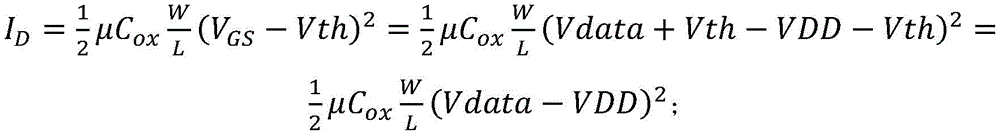
可知,工作电流的大小与驱动晶体管T1的阈值电压Vth无关,从而消除了阈值电压对工作电流的影响,实现了像素补偿。其中,该驱动晶体管T1的第一控制极的电位为(Vdata1+Vth),该驱动晶体管T1的第二控制极的电位为偏压信号Vdata2的电位值。It can be seen that the magnitude of the working current has nothing to do with the threshold voltage Vth of the driving transistor T1, thereby eliminating the influence of the threshold voltage on the working current and realizing pixel compensation. The potential of the first gate of the driving transistor T1 is (Vdata1+Vth), and the potential of the second gate of the driving transistor T1 is the potential of the bias signal Vdata2.
本公开实施方式还提供了一种像素电路的驱动方法,用于驱动上述实施方式所述的像素电路。该像素电路的驱动方法可以包括:如图1所示,数据信号模块1接收数据写入信号端GATE1提供的数据写入信号Gate1,并将数据信号端VDATA1提供的数据信号Vdata1传输至驱动晶体管T1;使偏压信号模块2在偏压写入信号端GATE2和偏压信号端VDATA2的控制下调节驱动晶体管T1的阈值电压。由于本公开实施方式的驱动方法所驱动的像素电路同上述实施方式中的像素电路相同,因此,其具有相同的有益效果,在此不再赘述。Embodiments of the present disclosure also provide a method for driving a pixel circuit, which is used to drive the pixel circuit described in the above-mentioned embodiments. The driving method of the pixel circuit may include: as shown in FIG. 1 , the
如图2所示,在偏压信号Vdata2传输至驱动晶体管T1的第二控制极后,驱动晶体管T1的阈值电压能够增大,以超出驱动晶体管T1的第一控制极与驱动晶体管T1的第二极之间的电势差;驱动晶体管T1的阈值电压也能够减小,以低于驱动晶体管T1的第一控制极与驱动晶体管T1的第二极之间的电势差。As shown in FIG. 2, after the bias signal Vdata2 is transmitted to the second gate of the driving transistor T1, the threshold voltage of the driving transistor T1 can be increased to exceed the first gate of the driving transistor T1 and the second gate of the driving transistor T1 The potential difference between the electrodes; the threshold voltage of the drive transistor T1 can also be reduced to be lower than the potential difference between the first control electrode of the drive transistor T1 and the second electrode of the drive transistor T1.
本公开实施方式还提供一种显示装置。如图1所示,该显示装置可以包括发光元件L0和上述任一项所述的像素电路。该发光元件L0的第一端连接于像素电路中驱动晶体管T1的第二极,第二端连接第二电源信号端VSS。该显示装置可以为手机、平板电脑、电视机、笔记本电脑、数码相框、导航仪等任何具有显示功能的产品或部件。由于本公开实施方式的显示装置中的像素电路同上述实施方式中的像素电路相同,因此,其具有相同的有益效果,在此不再赘述。Embodiments of the present disclosure also provide a display device. As shown in FIG. 1 , the display device may include a light-emitting element L0 and the pixel circuit described in any one of the above. The first terminal of the light-emitting element L0 is connected to the second pole of the driving transistor T1 in the pixel circuit, and the second terminal is connected to the second power signal terminal VSS. The display device can be any product or component with a display function, such as a mobile phone, a tablet computer, a TV, a notebook computer, a digital photo frame, a navigator, and the like. Since the pixel circuit in the display device of the embodiment of the present disclosure is the same as the pixel circuit in the above-mentioned embodiment, it has the same beneficial effects, and details are not repeated here.
以上所述仅是本发明的较佳实施方式而已,并非对本发明做任何形式上的限制,虽然本发明已以较佳实施方式揭露如上,然而并非用以限定本发明,任何熟悉本专业的技术人员,在不脱离本发明技术方案的范围内,当可利用上述揭示的技术内容做出些许更动或修饰为等同变化的等效实施方式,但凡是未脱离本发明技术方案的内容,依据本发明的技术实质对以上实施方式所作的任何简单修改、等同变化与修饰,均仍属于本发明技术方案的范围内。The above descriptions are only preferred embodiments of the present invention, and are not intended to limit the present invention in any form. Although the present invention has been disclosed above in preferred embodiments, it is not intended to limit the present invention. Personnel, without departing from the scope of the technical solution of the present invention, can make some changes or modifications to equivalent embodiments of equivalent changes by using the technical content disclosed above, provided that any content that does not depart from the technical solution of the present invention, according to the present invention Any simple modifications, equivalent changes and modifications made to the above embodiments by the technical essence of the invention still fall within the scope of the technical solutions of the present invention.
Claims (12)
Priority Applications (2)
| Application Number | Priority Date | Filing Date | Title |
|---|---|---|---|
| CN202110004616.6A CN114765007A (en) | 2021-01-04 | 2021-01-04 | Display device, pixel circuit and driving method thereof |
| US17/509,899 US11587501B2 (en) | 2021-01-04 | 2021-10-25 | Display apparatuses, pixel circuits and methods of driving pixel circuit |
Applications Claiming Priority (1)
| Application Number | Priority Date | Filing Date | Title |
|---|---|---|---|
| CN202110004616.6A CN114765007A (en) | 2021-01-04 | 2021-01-04 | Display device, pixel circuit and driving method thereof |
Publications (1)
| Publication Number | Publication Date |
|---|---|
| CN114765007A true CN114765007A (en) | 2022-07-19 |
Family
ID=82219801
Family Applications (1)
| Application Number | Title | Priority Date | Filing Date |
|---|---|---|---|
| CN202110004616.6A Pending CN114765007A (en) | 2021-01-04 | 2021-01-04 | Display device, pixel circuit and driving method thereof |
Country Status (2)
| Country | Link |
|---|---|
| US (1) | US11587501B2 (en) |
| CN (1) | CN114765007A (en) |
Cited By (1)
| Publication number | Priority date | Publication date | Assignee | Title |
|---|---|---|---|---|
| WO2025001206A1 (en) * | 2023-06-29 | 2025-01-02 | 合肥维信诺科技有限公司 | Pixel drive circuit, display panel, and display device |
Families Citing this family (3)
| Publication number | Priority date | Publication date | Assignee | Title |
|---|---|---|---|---|
| KR20220148972A (en) * | 2021-04-29 | 2022-11-08 | 삼성디스플레이 주식회사 | Pixel circuit and display device including the same |
| CN118015988A (en) * | 2024-02-29 | 2024-05-10 | 云谷(固安)科技有限公司 | Pixel circuit, pixel driving method, display panel and display device |
| KR20260007422A (en) * | 2024-07-04 | 2026-01-14 | 삼성디스플레이 주식회사 | Display apparatus |
Citations (9)
| Publication number | Priority date | Publication date | Assignee | Title |
|---|---|---|---|---|
| US20150171156A1 (en) * | 2013-12-12 | 2015-06-18 | Semiconductor Energy Laboratory Co., Ltd. | Light-emitting device |
| US20160042694A1 (en) * | 2014-08-07 | 2016-02-11 | Samsung Display Co., Ltd. | Pixel circuit and organic light-emitting diode display including the same |
| CN107767814A (en) * | 2017-11-27 | 2018-03-06 | 合肥鑫晟光电科技有限公司 | Image element circuit, display device and double grid driving transistor |
| CN108711398A (en) * | 2018-05-28 | 2018-10-26 | 京东方科技集团股份有限公司 | Pixel circuit and its driving method, array substrate, display panel |
| CN110021265A (en) * | 2019-04-26 | 2019-07-16 | 上海天马微电子有限公司 | Pixel circuit and driving method thereof, display device and driving method |
| CN110660829A (en) * | 2018-06-28 | 2020-01-07 | 三星显示有限公司 | Organic Light Emitting Diode Display Device |
| WO2020066024A1 (en) * | 2018-09-28 | 2020-04-02 | シャープ株式会社 | Display device and drive method therefor |
| CN111179850A (en) * | 2020-01-13 | 2020-05-19 | 深圳市华星光电半导体显示技术有限公司 | Pixel compensation circuit, array substrate and display panel |
| CN112150967A (en) * | 2020-10-20 | 2020-12-29 | 厦门天马微电子有限公司 | A display panel, driving method and display device |
Family Cites Families (2)
| Publication number | Priority date | Publication date | Assignee | Title |
|---|---|---|---|---|
| KR102091485B1 (en) * | 2013-12-30 | 2020-03-20 | 엘지디스플레이 주식회사 | Organic light emitting display device and method for driving thereof |
| KR102699490B1 (en) * | 2018-06-22 | 2024-08-27 | 삼성디스플레이 주식회사 | Organic light emitting diode display device |
-
2021
- 2021-01-04 CN CN202110004616.6A patent/CN114765007A/en active Pending
- 2021-10-25 US US17/509,899 patent/US11587501B2/en active Active
Patent Citations (9)
| Publication number | Priority date | Publication date | Assignee | Title |
|---|---|---|---|---|
| US20150171156A1 (en) * | 2013-12-12 | 2015-06-18 | Semiconductor Energy Laboratory Co., Ltd. | Light-emitting device |
| US20160042694A1 (en) * | 2014-08-07 | 2016-02-11 | Samsung Display Co., Ltd. | Pixel circuit and organic light-emitting diode display including the same |
| CN107767814A (en) * | 2017-11-27 | 2018-03-06 | 合肥鑫晟光电科技有限公司 | Image element circuit, display device and double grid driving transistor |
| CN108711398A (en) * | 2018-05-28 | 2018-10-26 | 京东方科技集团股份有限公司 | Pixel circuit and its driving method, array substrate, display panel |
| CN110660829A (en) * | 2018-06-28 | 2020-01-07 | 三星显示有限公司 | Organic Light Emitting Diode Display Device |
| WO2020066024A1 (en) * | 2018-09-28 | 2020-04-02 | シャープ株式会社 | Display device and drive method therefor |
| CN110021265A (en) * | 2019-04-26 | 2019-07-16 | 上海天马微电子有限公司 | Pixel circuit and driving method thereof, display device and driving method |
| CN111179850A (en) * | 2020-01-13 | 2020-05-19 | 深圳市华星光电半导体显示技术有限公司 | Pixel compensation circuit, array substrate and display panel |
| CN112150967A (en) * | 2020-10-20 | 2020-12-29 | 厦门天马微电子有限公司 | A display panel, driving method and display device |
Cited By (2)
| Publication number | Priority date | Publication date | Assignee | Title |
|---|---|---|---|---|
| WO2025001206A1 (en) * | 2023-06-29 | 2025-01-02 | 合肥维信诺科技有限公司 | Pixel drive circuit, display panel, and display device |
| US12431070B2 (en) | 2023-06-29 | 2025-09-30 | Hefei Visionox Technology Co., Ltd. | Pixel driving circuit and display panel |
Also Published As
| Publication number | Publication date |
|---|---|
| US11587501B2 (en) | 2023-02-21 |
| US20220215793A1 (en) | 2022-07-07 |
Similar Documents
| Publication | Publication Date | Title |
|---|---|---|
| CN113012643B (en) | Display panel, driving method thereof and display device | |
| CN107424570B (en) | Pixel unit circuit, pixel circuit, driving method and display device | |
| CN210378422U (en) | Pixel circuit and display device | |
| CN104821150B (en) | Image element circuit and its driving method and display device | |
| WO2023005597A1 (en) | Pixel drive circuit and display panel | |
| CN113851082B (en) | Pixel driving circuit, driving method thereof and display panel | |
| WO2023035613A1 (en) | Pixel circuit and driving method therefor, and display panel | |
| CN114765007A (en) | Display device, pixel circuit and driving method thereof | |
| CN114155813B (en) | Pixel circuit, driving method of pixel circuit and display panel | |
| US20210358390A1 (en) | Subpixel circuit, pixel circuit, driving method thereof, display module and display device | |
| CN107180612B (en) | A pixel circuit and a display panel | |
| WO2022061852A1 (en) | Pixel driving circuit and display panel | |
| JP2020519925A (en) | Pixel driving circuit, pixel driving method, and display device | |
| CN108470539A (en) | A kind of pixel circuit and its driving method, display panel and display device | |
| CN105575327B (en) | A kind of image element circuit, its driving method and organic EL display panel | |
| WO2019109673A1 (en) | Pixel circuit and driving method therefor, display panel and display device | |
| WO2019085485A1 (en) | Pixel circuit and driving method, and display device | |
| CN112820236B (en) | Pixel driving circuit, driving method thereof, display panel and display device | |
| WO2020020118A1 (en) | Pixel circuit and driving method thereof and display device | |
| CN113168806B (en) | Pixel driving circuit, pixel driving method, display panel and display device | |
| WO2024036897A1 (en) | Pixel compensation circuit and display panel | |
| WO2021083014A1 (en) | Pixel drive circuit and drive method therefor, display panel, and display apparatus | |
| WO2022022146A1 (en) | Pixel circuit and driving method therefor, display substrate, and display apparatus | |
| CN110223639A (en) | Pixel circuit, image element driving method, display base plate and display device | |
| WO2021196279A1 (en) | Pixel driving circuit and display panel |
Legal Events
| Date | Code | Title | Description |
|---|---|---|---|
| PB01 | Publication | ||
| PB01 | Publication | ||
| SE01 | Entry into force of request for substantive examination | ||
| SE01 | Entry into force of request for substantive examination |