CN114695612A - Gallium nitride-based light emitting diode epitaxial structure and preparation method thereof - Google Patents
Gallium nitride-based light emitting diode epitaxial structure and preparation method thereof Download PDFInfo
- Publication number
- CN114695612A CN114695612A CN202210610853.1A CN202210610853A CN114695612A CN 114695612 A CN114695612 A CN 114695612A CN 202210610853 A CN202210610853 A CN 202210610853A CN 114695612 A CN114695612 A CN 114695612A
- Authority
- CN
- China
- Prior art keywords
- layer
- quantum barrier
- quantum
- sublayer
- barrier layer
- Prior art date
- Legal status (The legal status is an assumption and is not a legal conclusion. Google has not performed a legal analysis and makes no representation as to the accuracy of the status listed.)
- Granted
Links
- 229910002601 GaN Inorganic materials 0.000 title claims abstract description 135
- JMASRVWKEDWRBT-UHFFFAOYSA-N Gallium nitride Chemical compound [Ga]#N JMASRVWKEDWRBT-UHFFFAOYSA-N 0.000 title claims abstract description 23
- 238000002360 preparation method Methods 0.000 title abstract description 16
- 230000004888 barrier function Effects 0.000 claims abstract description 130
- 229910002704 AlGaN Inorganic materials 0.000 claims abstract description 49
- 230000000903 blocking effect Effects 0.000 claims abstract description 41
- 239000000203 mixture Substances 0.000 claims abstract description 20
- 239000000758 substrate Substances 0.000 claims description 35
- 229910017911 MgIn Inorganic materials 0.000 claims description 30
- 239000000956 alloy Substances 0.000 claims description 30
- 229910045601 alloy Inorganic materials 0.000 claims description 30
- 238000000034 method Methods 0.000 claims description 23
- 230000006911 nucleation Effects 0.000 claims description 21
- 238000010899 nucleation Methods 0.000 claims description 21
- 230000007423 decrease Effects 0.000 claims description 4
- 238000004519 manufacturing process Methods 0.000 claims 2
- 238000005036 potential barrier Methods 0.000 abstract description 4
- 239000011777 magnesium Substances 0.000 description 44
- 238000006243 chemical reaction Methods 0.000 description 32
- OKTJSMMVPCPJKN-UHFFFAOYSA-N Carbon Chemical compound [C] OKTJSMMVPCPJKN-UHFFFAOYSA-N 0.000 description 26
- 229910002804 graphite Inorganic materials 0.000 description 26
- 239000010439 graphite Substances 0.000 description 26
- IJGRMHOSHXDMSA-UHFFFAOYSA-N Atomic nitrogen Chemical compound N#N IJGRMHOSHXDMSA-UHFFFAOYSA-N 0.000 description 18
- XCZXGTMEAKBVPV-UHFFFAOYSA-N trimethylgallium Chemical compound C[Ga](C)C XCZXGTMEAKBVPV-UHFFFAOYSA-N 0.000 description 15
- JLTRXTDYQLMHGR-UHFFFAOYSA-N trimethylaluminium Chemical compound C[Al](C)C JLTRXTDYQLMHGR-UHFFFAOYSA-N 0.000 description 10
- 230000000052 comparative effect Effects 0.000 description 9
- 229910052757 nitrogen Inorganic materials 0.000 description 9
- RGGPNXQUMRMPRA-UHFFFAOYSA-N triethylgallium Chemical compound CC[Ga](CC)CC RGGPNXQUMRMPRA-UHFFFAOYSA-N 0.000 description 9
- IBEFSUTVZWZJEL-UHFFFAOYSA-N trimethylindium Chemical compound C[In](C)C IBEFSUTVZWZJEL-UHFFFAOYSA-N 0.000 description 9
- 229910052749 magnesium Inorganic materials 0.000 description 8
- 235000012431 wafers Nutrition 0.000 description 8
- 238000005234 chemical deposition Methods 0.000 description 7
- 230000000737 periodic effect Effects 0.000 description 7
- 239000002019 doping agent Substances 0.000 description 6
- 239000000463 material Substances 0.000 description 6
- 229910052751 metal Inorganic materials 0.000 description 6
- 239000002184 metal Substances 0.000 description 6
- 229910052594 sapphire Inorganic materials 0.000 description 6
- 239000010980 sapphire Substances 0.000 description 6
- UFHFLCQGNIYNRP-UHFFFAOYSA-N Hydrogen Chemical compound [H][H] UFHFLCQGNIYNRP-UHFFFAOYSA-N 0.000 description 5
- 239000001257 hydrogen Substances 0.000 description 5
- 229910052739 hydrogen Inorganic materials 0.000 description 5
- 230000006798 recombination Effects 0.000 description 5
- 238000005215 recombination Methods 0.000 description 5
- FYYHWMGAXLPEAU-UHFFFAOYSA-N Magnesium Chemical compound [Mg] FYYHWMGAXLPEAU-UHFFFAOYSA-N 0.000 description 4
- 230000004913 activation Effects 0.000 description 4
- 229910052782 aluminium Inorganic materials 0.000 description 4
- XAGFODPZIPBFFR-UHFFFAOYSA-N aluminium Chemical compound [Al] XAGFODPZIPBFFR-UHFFFAOYSA-N 0.000 description 4
- 239000013078 crystal Substances 0.000 description 4
- 238000002347 injection Methods 0.000 description 4
- 239000007924 injection Substances 0.000 description 4
- 229910017083 AlN Inorganic materials 0.000 description 3
- BLRPTPMANUNPDV-UHFFFAOYSA-N Silane Chemical compound [SiH4] BLRPTPMANUNPDV-UHFFFAOYSA-N 0.000 description 3
- 239000004411 aluminium Substances 0.000 description 3
- 239000012159 carrier gas Substances 0.000 description 3
- 238000005229 chemical vapour deposition Methods 0.000 description 3
- 239000013256 coordination polymer Substances 0.000 description 3
- 239000007789 gas Substances 0.000 description 3
- 229910000077 silane Inorganic materials 0.000 description 3
- 229910052710 silicon Inorganic materials 0.000 description 3
- 239000010703 silicon Substances 0.000 description 3
- HBMJWWWQQXIZIP-UHFFFAOYSA-N silicon carbide Chemical compound [Si+]#[C-] HBMJWWWQQXIZIP-UHFFFAOYSA-N 0.000 description 3
- 229910010271 silicon carbide Inorganic materials 0.000 description 3
- 229910018509 Al—N Inorganic materials 0.000 description 2
- 239000012298 atmosphere Substances 0.000 description 2
- 230000009286 beneficial effect Effects 0.000 description 2
- 230000007547 defect Effects 0.000 description 2
- 230000005611 electricity Effects 0.000 description 2
- 239000012535 impurity Substances 0.000 description 2
- 238000010348 incorporation Methods 0.000 description 2
- 230000004941 influx Effects 0.000 description 2
- -1 magnesium tetracene Chemical compound 0.000 description 2
- 230000003446 memory effect Effects 0.000 description 2
- 239000012299 nitrogen atmosphere Substances 0.000 description 2
- 238000001556 precipitation Methods 0.000 description 2
- 230000008569 process Effects 0.000 description 2
- 230000001737 promoting effect Effects 0.000 description 2
- 238000007788 roughening Methods 0.000 description 2
- 239000004065 semiconductor Substances 0.000 description 2
- 239000000969 carrier Substances 0.000 description 1
- 230000003247 decreasing effect Effects 0.000 description 1
- 238000010586 diagram Methods 0.000 description 1
- 230000000694 effects Effects 0.000 description 1
- 229910052738 indium Inorganic materials 0.000 description 1
- APFVFJFRJDLVQX-UHFFFAOYSA-N indium atom Chemical compound [In] APFVFJFRJDLVQX-UHFFFAOYSA-N 0.000 description 1
- 238000012986 modification Methods 0.000 description 1
- 230000004048 modification Effects 0.000 description 1
Images


Classifications
-
- H—ELECTRICITY
- H10—SEMICONDUCTOR DEVICES; ELECTRIC SOLID-STATE DEVICES NOT OTHERWISE PROVIDED FOR
- H10H—INORGANIC LIGHT-EMITTING SEMICONDUCTOR DEVICES HAVING POTENTIAL BARRIERS
- H10H20/00—Individual inorganic light-emitting semiconductor devices having potential barriers, e.g. light-emitting diodes [LED]
- H10H20/80—Constructional details
- H10H20/81—Bodies
- H10H20/816—Bodies having carrier transport control structures, e.g. highly-doped semiconductor layers or current-blocking structures
- H10H20/8162—Current-blocking structures
-
- H—ELECTRICITY
- H10—SEMICONDUCTOR DEVICES; ELECTRIC SOLID-STATE DEVICES NOT OTHERWISE PROVIDED FOR
- H10H—INORGANIC LIGHT-EMITTING SEMICONDUCTOR DEVICES HAVING POTENTIAL BARRIERS
- H10H20/00—Individual inorganic light-emitting semiconductor devices having potential barriers, e.g. light-emitting diodes [LED]
- H10H20/01—Manufacture or treatment
- H10H20/011—Manufacture or treatment of bodies, e.g. forming semiconductor layers
- H10H20/013—Manufacture or treatment of bodies, e.g. forming semiconductor layers having light-emitting regions comprising only Group III-V materials
- H10H20/0133—Manufacture or treatment of bodies, e.g. forming semiconductor layers having light-emitting regions comprising only Group III-V materials with a substrate not being Group III-V materials
-
- H—ELECTRICITY
- H10—SEMICONDUCTOR DEVICES; ELECTRIC SOLID-STATE DEVICES NOT OTHERWISE PROVIDED FOR
- H10H—INORGANIC LIGHT-EMITTING SEMICONDUCTOR DEVICES HAVING POTENTIAL BARRIERS
- H10H20/00—Individual inorganic light-emitting semiconductor devices having potential barriers, e.g. light-emitting diodes [LED]
- H10H20/01—Manufacture or treatment
- H10H20/011—Manufacture or treatment of bodies, e.g. forming semiconductor layers
- H10H20/013—Manufacture or treatment of bodies, e.g. forming semiconductor layers having light-emitting regions comprising only Group III-V materials
- H10H20/0137—Manufacture or treatment of bodies, e.g. forming semiconductor layers having light-emitting regions comprising only Group III-V materials the light-emitting regions comprising nitride materials
-
- H—ELECTRICITY
- H10—SEMICONDUCTOR DEVICES; ELECTRIC SOLID-STATE DEVICES NOT OTHERWISE PROVIDED FOR
- H10H—INORGANIC LIGHT-EMITTING SEMICONDUCTOR DEVICES HAVING POTENTIAL BARRIERS
- H10H20/00—Individual inorganic light-emitting semiconductor devices having potential barriers, e.g. light-emitting diodes [LED]
- H10H20/80—Constructional details
- H10H20/81—Bodies
- H10H20/811—Bodies having quantum effect structures or superlattices, e.g. tunnel junctions
- H10H20/812—Bodies having quantum effect structures or superlattices, e.g. tunnel junctions within the light-emitting regions, e.g. having quantum confinement structures
-
- H—ELECTRICITY
- H10—SEMICONDUCTOR DEVICES; ELECTRIC SOLID-STATE DEVICES NOT OTHERWISE PROVIDED FOR
- H10H—INORGANIC LIGHT-EMITTING SEMICONDUCTOR DEVICES HAVING POTENTIAL BARRIERS
- H10H20/00—Individual inorganic light-emitting semiconductor devices having potential barriers, e.g. light-emitting diodes [LED]
- H10H20/80—Constructional details
- H10H20/81—Bodies
- H10H20/822—Materials of the light-emitting regions
- H10H20/824—Materials of the light-emitting regions comprising only Group III-V materials, e.g. GaP
- H10H20/825—Materials of the light-emitting regions comprising only Group III-V materials, e.g. GaP containing nitrogen, e.g. GaN
- H10H20/8252—Materials of the light-emitting regions comprising only Group III-V materials, e.g. GaP containing nitrogen, e.g. GaN characterised by the dopants
Landscapes
- Led Devices (AREA)
Abstract
本发明提供一种氮化镓基发光二极管外延结构及其制备方法,外延结构包括多量子阱层,所述多量子阱层包括周期性依次层叠的多个量子阱层及量子垒层;所述量子垒层包括第一量子垒层和第二量子垒层,所述第二量子垒层包括交替生长的多个第一子层及第二子层,所述第一子层与所述量子阱层接触,所述第二子层或所述第一子层与所述P型AlGaN电子阻挡层接触。本发明第二量子垒层中第一子层AlxGa1‑xN层中Al组分越高,势垒高度越高,越有能力阻挡电子溢出到P型GaN层,便于更多的空穴向多量子阱层中的发光层注入,进一步提高电子和空穴在多量子阱层的有效发光。
The invention provides an epitaxial structure of a gallium nitride-based light-emitting diode and a preparation method thereof. The epitaxial structure includes a multi-quantum well layer, and the multi-quantum well layer includes a plurality of quantum well layers and quantum barrier layers that are periodically stacked in sequence; the The quantum barrier layer includes a first quantum barrier layer and a second quantum barrier layer, the second quantum barrier layer includes a plurality of first sublayers and second sublayers grown alternately, the first sublayer and the quantum well layer contact, the second sublayer or the first sublayer is in contact with the P-type AlGaN electron blocking layer. In the second quantum barrier layer of the present invention, the higher the Al composition in the Al x Ga 1-x N layer of the first sublayer, the higher the potential barrier height, the better the ability to prevent electrons from overflowing into the P-type GaN layer, which is convenient for more empty space. The holes are injected into the light-emitting layer in the multi-quantum well layer, which further improves the effective light emission of electrons and holes in the multi-quantum well layer.
Description
技术领域technical field
本发明涉及芯片技术领域,特别涉及一种氮化镓基发光二极管外延结构及其制备方法。The invention relates to the field of chip technology, in particular to a gallium nitride-based light emitting diode epitaxial structure and a preparation method thereof.
背景技术Background technique
发光二极管(LED,Light Emitting Diode)是一种半导体固体发光器件,其利用半导体 PN结作为发光材料,可以直接将电转换为光。GaN基的发光二极管(LED)被广泛的应用于日用照明、手机背光、汽车车灯等领域。A light-emitting diode (LED, Light Emitting Diode) is a semiconductor solid-state light-emitting device, which uses a semiconductor PN junction as a light-emitting material and can directly convert electricity into light. GaN-based light-emitting diodes (LEDs) are widely used in daily lighting, mobile phone backlights, automotive lights and other fields.
而制备LED外延片是其中制备发光二极管的重要环节,目前 GaN基LED外延片包括衬底、依次层叠在衬底上的缓冲层、三维成核层、未掺杂的GaN层、N型GaN层、多量子阱层、P型AlGaN电子阻挡层、P型接触层。其中,多量子阱层包括交替生长的InGaN势阱层和GaN势垒层,P型AlGaN电子阻挡层为P 型AlGaN层。The preparation of LED epitaxial wafers is an important link in the preparation of light-emitting diodes. At present, GaN-based LED epitaxial wafers include a substrate, a buffer layer sequentially stacked on the substrate, a three-dimensional nucleation layer, an undoped GaN layer, and an N-type GaN layer. , Multiple quantum well layer, P-type AlGaN electron blocking layer, P-type contact layer. The multiple quantum well layer includes alternately grown InGaN well layers and GaN barrier layers, and the P-type AlGaN electron blocking layer is a P-type AlGaN layer.
但是当前的外延结构中,由于电子具有较小的有效质量和较高的迁移率,所以电子的移动速率是远远大于空穴的,而且由于电子的数量也是大于空穴的数量,因此在大电流工作条件下,LED会出现电子溢流,电子会越过多量子阱层跑到P型GaN层出现非辐射复合,从而导致LED的发光效率低。However, in the current epitaxial structure, due to the small effective mass and high mobility of electrons, the movement rate of electrons is much higher than that of holes, and since the number of electrons is also greater than the number of holes, in large Under current working conditions, the LED will overflow with electrons, and the electrons will cross the multi-quantum well layer and run to the P-type GaN layer for non-radiative recombination, resulting in low luminous efficiency of the LED.
发明内容SUMMARY OF THE INVENTION
基于此,本发明的目的是提供一种氮化镓基发光二极管外延结构及其制备方法,用于解决现有技术中由于LED会出现电子溢流从而导致LED的发光效率低的技术问题。Based on this, the purpose of the present invention is to provide a gallium nitride-based light emitting diode epitaxial structure and a preparation method thereof, which are used to solve the technical problem of low luminous efficiency of LED due to electron overflow in the LED in the prior art.
本申请一方面提供一种氮化镓基发光二极管外延结构,包括依次层叠的衬底、缓冲层、三维成核层、未掺杂的GaN层、N型GaN层、多量子阱层、P型AlGaN电子阻挡层、P型GaN层以及P型接触层,所述多量子阱层包括周期性依次层叠的多个量子阱层及量子垒层,多个所述量子阱层中的最底部一量子阱层层叠于所述N型GaN层上方;In one aspect of the present application, an epitaxial structure of a gallium nitride-based light-emitting diode is provided, which includes a substrate, a buffer layer, a three-dimensional nucleation layer, an undoped GaN layer, an N-type GaN layer, a multiple quantum well layer, and a P-type layer stacked in sequence. An AlGaN electron blocking layer, a P-type GaN layer and a P-type contact layer, the multiple quantum well layer includes a plurality of quantum well layers and quantum barrier layers that are periodically stacked in sequence, and a quantum well layer at the bottom of the multiple quantum well layers a well layer is stacked above the N-type GaN layer;
所述量子垒层包括第一量子垒层和第二量子垒层,其中,所述第二量子垒层为多个所述量子垒层中最靠近所述P型AlGaN电子阻挡层的一量子垒层,所述第一量子垒层为除所述第二量子垒层之外的其他量子垒层;The quantum barrier layer includes a first quantum barrier layer and a second quantum barrier layer, wherein the second quantum barrier layer is a quantum barrier closest to the P-type AlGaN electron blocking layer among the plurality of quantum barrier layers layer, the first quantum barrier layer is other quantum barrier layers except the second quantum barrier layer;
所述第二量子垒层包括交替生长的多个第一子层及第二子层,多个所述第一子层中的最底部一第一子层与最靠近所述第二量子垒层的一量子阱层接触,所述第二量子垒层中的最顶层与所述P型AlGaN电子阻挡层接触,所述第二量子垒层中的最顶层为第二子层或第一子层;The second quantum barrier layer includes a plurality of first sublayers and second sublayers grown alternately, and the bottommost first sublayer among the plurality of first sublayers is the closest to the second quantum barrier layer A quantum well layer of the second quantum well layer is in contact, the topmost layer in the second quantum barrier layer is in contact with the P-type AlGaN electron blocking layer, and the topmost layer in the second quantum barrier layer is the second sublayer or the first sublayer ;
其中,所述第一量子垒层为GaN层,所述量子阱层为InGaN层,所述第一子层为AlxGa1-xN层,其中,0.05<x<1,所述第二子层为MgIn合金层。Wherein, the first quantum barrier layer is a GaN layer, the quantum well layer is an InGaN layer, and the first sublayer is an AlxGa1 - xN layer, wherein 0.05<x<1, the second The sublayer is a MgIn alloy layer.
另外,根据本申请上述的氮化镓基发光二极管外延结构,还可以具有如下附加的技术特征:In addition, according to the above-mentioned gallium nitride-based light-emitting diode epitaxial structure of the present application, the following additional technical features may also be provided:
进一步地,所述第一子层的厚度为3-8nm;所述第二子层的厚度为1-3nm。Further, the thickness of the first sub-layer is 3-8 nm; the thickness of the second sub-layer is 1-3 nm.
进一步地,在所述MgIn合金层中:Further, in the MgIn alloy layer:
Mg掺杂浓度范围为1×10¹⁹/cm3~8×1020/cm3;The Mg doping concentration ranges from 1×10 19 /cm 3 to 8×10 20 /cm 3 ;
In掺杂浓度范围为8×10¹⁷/cm3~5×1018/cm3。The In doping concentration ranges from 8×10 17 /cm 3 to 5×10 18 /cm 3 .
本申请另一方面提供一种氮化镓基发光二极管外延结构制备方法,用于制备上述的氮化镓基发光二极管外延结构,所述方法包括:Another aspect of the present application provides a method for preparing an epitaxial structure of a gallium nitride-based light-emitting diode, which is used for preparing the above-mentioned epitaxial structure of a gallium nitride-based light-emitting diode, and the method includes:
获取一衬底;obtain a substrate;
在所述衬底上依次生长缓冲层、三维成核层、未掺杂的GaN层、N型GaN层、多量子阱层、P型AlGaN电子阻挡层、P型GaN层以及P型接触层;A buffer layer, a three-dimensional nucleation layer, an undoped GaN layer, an N-type GaN layer, a multiple quantum well layer, a P-type AlGaN electron blocking layer, a P-type GaN layer and a P-type contact layer are sequentially grown on the substrate;
在生长所述多量子阱层的步骤中,生长方法包括:In the step of growing the multiple quantum well layer, the growth method includes:
周期性依次层叠多个量子阱层及量子垒层以生长所述多量子阱层,其中,所述量子垒层包括第一量子垒层和第二量子垒层,所述第二量子垒层为多个所述量子垒层中最靠近所述P型AlGaN电子阻挡层的一量子垒层,所述第一量子垒层为除所述第二量子垒层之外的其他量子垒层;Periodically stack multiple quantum well layers and quantum barrier layers in sequence to grow the multiple quantum well layers, wherein the quantum barrier layer includes a first quantum barrier layer and a second quantum barrier layer, and the second quantum barrier layer is A quantum barrier layer that is closest to the P-type AlGaN electron blocking layer among the plurality of quantum barrier layers, and the first quantum barrier layer is another quantum barrier layer except the second quantum barrier layer;
在生长所述第二量子垒层的步骤中,生长方法包括:In the step of growing the second quantum barrier layer, the growing method includes:
交替生长多个第一子层及第二子层以生长所述第二量子垒层,其中,多个所述第一子层中的最底部一第一子层与最靠近所述第二量子垒层的一量子阱层接触,所述第二量子垒层中的最顶层与所述P型AlGaN电子阻挡层接触,所述第二量子垒层中的最顶层为第二子层或第一子层。A plurality of first sublayers and second sublayers are alternately grown to grow the second quantum barrier layer, wherein the bottommost first sublayer among the plurality of first sublayers is the closest to the second quantum barrier A quantum well layer of the barrier layer is in contact, the topmost layer in the second quantum barrier layer is in contact with the P-type AlGaN electron blocking layer, and the topmost layer in the second quantum barrier layer is the second sublayer or the first sublayer sublayer.
另外,根据本申请上述的氮化镓基发光二极管外延结构制备方法,还可以具有如下附加的技术特征:In addition, according to the above-mentioned preparation method of the gallium nitride-based light-emitting diode epitaxial structure of the present application, the following additional technical features may also be provided:
进一步地,所述第一量子垒层为GaN层,所述量子阱层为InGaN层,所述第一子层为AlxGa1-xN层,其中,0.05<x<1,所述第二子层为MgIn合金层。Further, the first quantum barrier layer is a GaN layer, the quantum well layer is an InGaN layer, and the first sublayer is an AlxGa1 - xN layer, wherein 0.05<x<1, the first sublayer is an AlxGa1-xN layer. The second sublayer is a MgIn alloy layer.
进一步地,在所述AlxGa1-xN层中,AlxGa1-xN层的Al组分随着交替生长周期的增加逐渐递增,或AlxGa1-xN层的Al组分随着交替生长周期的增加而固定不变。Further, in the AlxGa1 - xN layer, the Al composition of the AlxGa1 - xN layer is gradually increased with the increase of the alternate growth period, or the Al composition of the AlxGa1 - xN layer is gradually increased. The fractions were fixed with increasing alternating growth cycles.
进一步地,在所述MgIn合金层中,Mg的掺杂浓度随着交替生长周期的增加而逐渐递增,或Mg的掺杂浓度随着交替生长周期的增加而固定不变。Further, in the MgIn alloy layer, the doping concentration of Mg gradually increases with the increase of the alternate growth period, or the doping concentration of Mg is fixed with the increase of the alternate growth period.
进一步地,在所述MgIn合金层中,In的掺杂浓度随着交替生长周期的增加而逐渐递减,或In的掺杂浓度随着交替生长周期的增加而固定不变。Further, in the MgIn alloy layer, the doping concentration of In gradually decreases with the increase of the alternate growth period, or the doping concentration of In is fixed with the increase of the alternate growth period.
进一步地,所述第一子层和所述第二子层的生长温度随着交替生长周期的增加而逐渐递增,或随着交替生长周期的增加而固定不变。Further, the growth temperature of the first sublayer and the second sublayer is gradually increased with the increase of the alternate growth period, or fixed with the increase of the alternate growth period.
上述氮化镓基发光二极管外延结构及用于制备该氮化镓基发光二极管外延结构的制备方法具有如下有益效果:The above-mentioned gallium nitride-based light-emitting diode epitaxial structure and the preparation method for preparing the gallium nitride-based light-emitting diode epitaxial structure have the following beneficial effects:
1.本发明第二量子垒层中的第一子层AlxGa1-xN层与量子阱层接触,可以阻挡前面m个周期的量子阱层中In的析出,并且通过调节第一子层AlxGa1-xN层的Al组分,进一步提高势垒高度阻挡电子溢出到P型GaN层中而发出非辐射复合。1. The first sublayer Al x Ga 1-x N layer in the second quantum barrier layer of the present invention is in contact with the quantum well layer, which can block the precipitation of In in the quantum well layers of the previous m periods, and by adjusting the first sublayer The Al composition of the AlxGa1 - xN layer further increases the barrier height and prevents electrons from overflowing into the P-type GaN layer and emits non-radiative recombination.
2.本发明第二量子垒层中第二子层MgIn合金层和第一子层AlxGa1-xN层交替生长可以阻挡Mg扩散至前面多量子阱层中去。但是第一子层AlxGa1-xN层由于Al-N键能较大(2.8eV)导致Al原子的表面迁移率较低,抑制了外延层的侧向成长,因此Al吸附原子很难在外延面上迁移到台阶和扭折等低能量处形核,这造成了AlxGa1-xN层表面粗化严重,晶体质量差,而和第一子层AlxGa1-xN层交替生长的第二子层MgIn合金层,由于In原子并没有成为组份并入到AlxGa1-xN晶体中,In原子的加入,使得AlxGa1-xN层表面N自由键饱和,从而降低AlxGa1-xN层的表面能,提高Al原子的表面的迁移率,大幅度的降低了晶界和位错缺陷,促进了外延层的侧向生长速率, AlxGa1-xN层表面更平滑,界面粗糙度大幅度降低。2. The alternate growth of the second sublayer MgIn alloy layer and the first sublayer AlxGa1 -xN layer in the second quantum barrier layer of the present invention can prevent Mg from diffusing into the previous multiple quantum well layer. However, due to the large Al-N bond energy (2.8 eV) of the first sublayer Al x Ga 1-x N layer, the surface mobility of Al atoms is low, which inhibits the lateral growth of the epitaxial layer, so it is difficult for Al adatoms On the epitaxial surface, it migrates to low-energy places such as steps and kinks to form nucleation, which results in severe surface roughening of the Al x Ga 1-x N layer and poor crystal quality. The second sub-layer MgIn alloy layer with alternate growth layers, since In atoms are not incorporated into the AlxGa1 - xN crystal, the addition of In atoms makes the surface of the AlxGa1 - xN layer N free bond saturation, thereby reducing the surface energy of the Al x Ga 1-x N layer, improving the mobility of the surface of Al atoms, greatly reducing grain boundary and dislocation defects, and promoting the lateral growth rate of the epitaxial layer, Al x The surface of the Ga 1-x N layer is smoother, and the interface roughness is greatly reduced.
3. 本发明第二量子垒层中第一子层AlxGa1-xN层中Al组分越高,势垒高度越高,越有能力阻挡电子溢出到P型GaN层。但是高Al组分的AlxGa1-xN层其电离能越高,电导率越低,而和第一子层AlxGa1-xN层交替生长的第二子层MgIn合金层,In的掺入,可以降低Mg的活化能,Mg的激活效率提高,Mg存在记忆效应,会形成Mg拖尾现象扩散到m个周期量子阱中,进而可以显著提高对前面m个周期的多量子层空穴注入以及空穴浓度,便于更多的空穴向多量子阱层中的发光层注入,进一步提高电子和空穴在多量子阱层的有效发光。3. The higher the Al composition in the first sublayer Al x Ga 1-x N layer in the second quantum barrier layer of the present invention, the higher the potential barrier height, and the better the ability to prevent electrons from overflowing to the P-type GaN layer. However, the Al x Ga 1-x N layer with high Al composition has a higher ionization energy and a lower conductivity, and the second sub-layer MgIn alloy layer grown alternately with the first sub-layer Al x Ga 1-x N layer, Incorporation of In can reduce the activation energy of Mg, improve the activation efficiency of Mg, and Mg has a memory effect, which will form a Mg tailing phenomenon that diffuses into m-period quantum wells, which can significantly improve the multi-quantum performance of the previous m periods. Layer hole injection and hole concentration facilitate the injection of more holes into the light-emitting layer in the multi-quantum well layer, and further improve the effective light emission of electrons and holes in the multi-quantum well layer.
附图说明Description of drawings
图1为本发明中氮化镓基发光二极管外延结构的结构示意图;1 is a schematic structural diagram of an epitaxial structure of a GaN-based light-emitting diode according to the present invention;
图2为本发明中多量子阱层的结构示意图;Fig. 2 is the structural representation of the multiple quantum well layer in the present invention;
主要结构符号说明:Description of main structure symbols:

如下具体实施方式将结合上述附图进一步说明本发明。The following specific embodiments will further illustrate the present invention in conjunction with the above drawings.
具体实施方式Detailed ways
为了便于理解本发明,下面将参照相关附图对本发明进行更全面的描述。附图中给出了本发明的若干实施例。但是,本发明可以以许多不同的形式来实现,并不限于本文所描述的实施例。相反地,提供这些实施例的目的是使对本发明的公开内容更加透彻全面。In order to facilitate understanding of the present invention, the present invention will be described more fully hereinafter with reference to the related drawings. Several embodiments of the invention are presented in the accompanying drawings. However, the present invention may be embodied in many different forms and is not limited to the embodiments described herein. Rather, these embodiments are provided so that this disclosure will be thorough and complete.
除非另有定义,本文所使用的所有的技术和科学术语与属于本发明的技术领域的技术人员通常理解的含义相同。本文中在本发明的说明书中所使用的术语只是为了描述具体的实施例的目的,不是旨在于限制本发明。本文所使用的术语“及/或”包括一个或多个相关的所列项目的任意的和所有的组合。Unless otherwise defined, all technical and scientific terms used herein have the same meaning as commonly understood by one of ordinary skill in the art to which this invention belongs. The terms used herein in the description of the present invention are for the purpose of describing specific embodiments only, and are not intended to limit the present invention. As used herein, the term "and/or" includes any and all combinations of one or more of the associated listed items.
目前业界氮化镓基发光二极管的主要难点是:因为电子具有较小的有效质量和较高的迁移率,所以电子的移动速率是远远大于空穴的,而且由于电子的数量也是大于空穴的数量,因此在大电流工作条件下,LED会出现电子溢流,电子会越过多量子阱层跑到P型GaN层出现非辐射复合。所以在传统的氮化镓基发光二极管的外延结构都是依靠在P型GaN层之前生长一层P型AlGaN电子阻挡层,通过调节外延结构中的P型AlGaN电子阻挡层的Al组分可以起到提高势垒高度,降低电子溢流,以提高载流子在多量子阱层复合效率的作用,但是高Al组分的AlGaN材料做P型掺杂非常困难,P型GaN中Mg掺杂的电离能在250emV已经非常高,当P型AlGaN电子阻挡层中的Al组分进一步提高时,例如,当Al组分达到15-20%时,P型AlGaN电子阻挡层甚至很难导电。At present, the main difficulty of GaN-based light-emitting diodes in the industry is: because electrons have small effective mass and high mobility, the movement rate of electrons is much higher than that of holes, and the number of electrons is also greater than that of holes. Therefore, under high current operating conditions, the LED will overflow with electrons, and the electrons will cross the multi-quantum well layer and run to the P-type GaN layer for non-radiative recombination. Therefore, in the traditional epitaxial structure of GaN-based light-emitting diodes, a P-type AlGaN electron blocking layer is grown before the P-type GaN layer. By adjusting the Al composition of the P-type AlGaN electron blocking layer in the epitaxial structure, the To increase the height of the potential barrier and reduce the overflow of electrons, so as to improve the effect of carriers in the recombination efficiency of the multi-quantum well layer, but it is very difficult to do P-type doping of AlGaN materials with high Al composition. The ionization energy is already very high at 250emV, and when the Al composition in the P-type AlGaN electron blocking layer is further increased, for example, when the Al composition reaches 15-20%, the P-type AlGaN electron blocking layer even hardly conducts electricity.
故在本申请中,提出一种氮化镓基发光二极管外延结构及其制备方法,用于解决现有技术中由于LED会出现电子溢流从而导致LED的发光效率低的技术问题。Therefore, in this application, an epitaxial structure of a gallium nitride-based light emitting diode and a preparation method thereof are proposed, which are used to solve the technical problem of low luminous efficiency of LED due to electron overflow in the LED in the prior art.
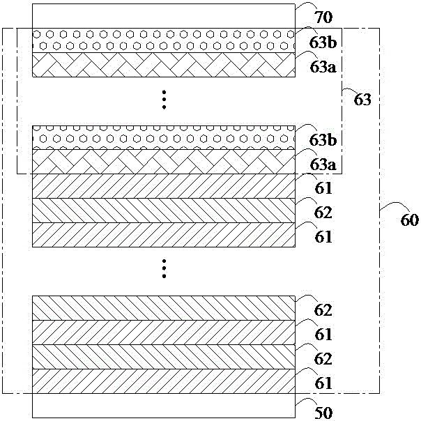
具体的,本申请一方面提供一种氮化镓基发光二极管外延结构,包括依次层叠的衬底10、缓冲层20、三维成核层30、未掺杂的GaN层40、N型GaN层50、多量子阱层60、P型AlGaN电子阻挡层70、P型GaN层80以及P型接触层90,所述多量子阱层60包括周期性依次层叠的多个量子阱层61及量子垒层,多个所述量子阱层61中的最底部一量子阱层层叠于所述N型GaN层50上方;Specifically, in one aspect of the present application, an epitaxial structure of a GaN-based light-emitting diode is provided, which includes a
所述量子垒层包括第一量子垒层62和第二量子垒层63,其中,所述第二量子垒层63为多个所述量子垒层中最靠近所述P型AlGaN电子阻挡层70的一量子垒层,所述第一量子垒层62为除所述第二量子垒层63之外的其他量子垒层;The quantum barrier layer includes a first
所述第二量子垒层63包括交替生长的多个第一子层63a及第二子层63b,多个所述第一子层63a中的最底部一第一子层与最靠近所述第二量子垒层63的一量子阱层接触,所述第二量子垒层63中的最顶层与所述P型AlGaN电子阻挡层70接触,所述第二量子垒层63中的最顶层为第二子层63b或第一子层63a。The second
进一步地,所述第一量子垒层62为GaN层,所述量子阱层61为InGaN层,所述第一子层63a为AlxGa1-xN层,其中,0.05<x<1,所述第二子层63b为MgIn合金层。Further, the first
进一步地,所述第一子层63a的厚度为3-8nm;所述第二子层63b的厚度为1-3nm。Further, the thickness of the
进一步地,在所述MgIn合金层中:Further, in the MgIn alloy layer:
Mg掺杂浓度范围为1×10¹⁹/cm3~8×1020/cm3;The Mg doping concentration ranges from 1×10 19 /cm 3 to 8×10 20 /cm 3 ;
In掺杂浓度范围为8×10¹⁷ /cm3~5×1018/cm3。The In doping concentration ranges from 8×10 17 /cm 3 to 5×10 18 /cm 3 .
本申请另一方面提供一种氮化镓基发光二极管外延结构制备方法,用于制备上述的氮化镓基发光二极管外延结构,所述方法包括:Another aspect of the present application provides a method for preparing an epitaxial structure of a gallium nitride-based light-emitting diode, which is used for preparing the above-mentioned epitaxial structure of a gallium nitride-based light-emitting diode, and the method includes:
获取一衬底;obtain a substrate;
在所述衬底上依次生长缓冲层、三维成核层、未掺杂的GaN层、N型GaN层、多量子阱层、P型AlGaN电子阻挡层、P型GaN层以及P型接触层;A buffer layer, a three-dimensional nucleation layer, an undoped GaN layer, an N-type GaN layer, a multiple quantum well layer, a P-type AlGaN electron blocking layer, a P-type GaN layer and a P-type contact layer are sequentially grown on the substrate;
在生长所述多量子阱层的步骤中,生长方法包括:In the step of growing the multiple quantum well layer, the growth method includes:
周期性依次层叠多个量子阱层及量子垒层以生长所述多量子阱层,其中,所述量子垒层包括第一量子垒层和第二量子垒层,所述第二量子垒层为多个所述量子垒层中最靠近所述P型AlGaN电子阻挡层的一量子垒层,所述第一量子垒层为除所述第二量子垒层之外的其他量子垒层;Periodically stack multiple quantum well layers and quantum barrier layers in sequence to grow the multiple quantum well layers, wherein the quantum barrier layer includes a first quantum barrier layer and a second quantum barrier layer, and the second quantum barrier layer is A quantum barrier layer that is closest to the P-type AlGaN electron blocking layer among the plurality of quantum barrier layers, and the first quantum barrier layer is another quantum barrier layer except the second quantum barrier layer;
在生长所述第二量子垒层的步骤中,生长方法包括:In the step of growing the second quantum barrier layer, the growing method includes:
交替生长多个第一子层及第二子层以生长所述第二量子垒层,其中,多个所述第一子层中的最底部一第一子层与最靠近所述第二量子垒层的一量子阱层接触,所述第二量子垒层中的最顶层与所述P型AlGaN电子阻挡层接触,所述第二量子垒层中的最顶层为第二子层或第一子层。A plurality of first sublayers and second sublayers are alternately grown to grow the second quantum barrier layer, wherein the bottommost first sublayer among the plurality of first sublayers is the closest to the second quantum barrier A quantum well layer of the barrier layer is in contact, the topmost layer in the second quantum barrier layer is in contact with the P-type AlGaN electron blocking layer, and the topmost layer in the second quantum barrier layer is the second sublayer or the first sublayer sublayer.
具体地,所述第一量子垒层为GaN层,所述量子阱层为InGaN层,所述第一子层为AlxGa1-xN层,其中,0.05<x<1,所述第二子层为MgIn合金层。Specifically, the first quantum barrier layer is a GaN layer, the quantum well layer is an InGaN layer, and the first sublayer is an AlxGa1 - xN layer, wherein 0.05<x<1, the first sublayer is The second sublayer is a MgIn alloy layer.
进一步地,所述第一子层和所述第二子层的生长温度随着交替生长周期的增加而逐渐递增,或随着交替生长周期的增加而固定不变。Further, the growth temperature of the first sublayer and the second sublayer is gradually increased with the increase of the alternate growth period, or fixed with the increase of the alternate growth period.
在所述AlxGa1-xN层中,AlxGa1-xN层的Al组分随着交替生长周期的增加逐渐递增,或AlxGa1-xN层的Al组分随着交替生长周期的增加而固定不变;In the AlxGa1 - xN layer, the Al composition of the AlxGa1 - xN layer gradually increases as the alternate growth period increases, or the Al composition of the AlxGa1 - xN layer increases with Alternating growth cycles increase and remain constant;
在所述MgIn合金层中, Mg的掺杂浓度随着交替生长周期的增加而逐渐递增,或Mg的掺杂浓度随着交替生长周期的增加而固定不变;In的掺杂浓度随着交替生长周期的增加而逐渐递减,或In的掺杂浓度随着交替生长周期的增加而固定不变。In the MgIn alloy layer, the doping concentration of Mg gradually increases with the increase of the alternate growth period, or the doping concentration of Mg is fixed with the increase of the alternate growth period; the doping concentration of In increases with the alternating growth period. It gradually decreases with the increase of the growth period, or the doping concentration of In is fixed with the increase of the alternate growth period.
具体地,氮化镓基发光二极管外延结构制备方法包括如下步骤:Specifically, the method for preparing an epitaxial structure of a gallium nitride-based light-emitting diode includes the following steps:
制备缓冲层:采用金属有机气相化学沉积方法在该衬底上沉积AlN缓冲层或GaN缓冲层或AlGaN缓冲层,通入高纯NH3作为N(氮)源,通入三甲基镓(TMGa)作为Ga源,通入三甲基铝(TMAl)作为铝源,生长压力为60-200torr,用于制备一种衬底生长的AlN或GaN或AlGaN的缓冲层。Preparation of buffer layer: AlN buffer layer or GaN buffer layer or AlGaN buffer layer is deposited on the substrate by metal organic vapor chemical deposition method, high-purity NH 3 is used as N (nitrogen) source, and trimethyl gallium (TMGa ) as a Ga source, with trimethylaluminum (TMAl) as an aluminum source, and a growth pressure of 60-200 torr, for preparing a buffer layer of AlN or GaN or AlGaN grown on a substrate.
制备三维成核层:采用金属有机气相化学沉积方法在缓冲层上通入三甲基镓(TMGa)作为Ga源,生长温度升高到1060-1090℃,在缓冲层上生长三维成核层;Preparation of three-dimensional nucleation layer: using metal organic vapor chemical deposition method to pass trimethyl gallium (TMGa) as Ga source on the buffer layer, the growth temperature is increased to 1060-1090 ℃, and the three-dimensional nucleation layer is grown on the buffer layer;
制备未掺杂的GaN层:采用金属有机气相化学沉积方法在GaN缓冲层上,通入三甲基镓作为Ga源,生长温度升高到1100-1125℃,在三维成核层上生长未掺杂的GaN层;Preparation of undoped GaN layer: using metal organic vapor chemical deposition method on the GaN buffer layer, feeding trimethylgallium as Ga source, increasing the growth temperature to 1100-1125 °C, and growing undoped GaN on the three-dimensional nucleation layer Impurity GaN layer;
制备N型GaN层:采用金属有机气相化学沉积方法,以SiH4作为掺杂源, 通入三甲基镓作为Ga源,生长温度降低到1095-1100℃,Si的掺杂浓度为1×10¹⁹/cm3-1×1020/cm3,在未掺杂的GaN层上生长N型GaN层;Preparation of N-type GaN layer: adopt metal organic vapor chemical deposition method, use SiH 4 as doping source, pass trimethyl gallium as Ga source, reduce the growth temperature to 1095-1100 ℃, and the doping concentration of Si is 1 × 10 19 /cm 3 -1×10 20 /cm 3 , growing an N-type GaN layer on the undoped GaN layer;
制备m+1个周期性的多量子阱层,其中m是大于0的正整数:采用金属有机气相化学沉积方法,通入三乙基镓作为Ga源,生长GaN垒层,随后通入三甲基铟源作为In源,三乙基镓作为Ga源,在GaN垒生长InyGa1-yN阱层,y=0.05-0.30,以此为量子阱层的一单位周期,整个多量子阱层由m+1(5≤m≤8)个周期构成,在生长完前m个周期的多量子阱层后,生长最后一个周期的InyGa1-yN层生长n个周期性层叠交替的第一子层和第二子层(其中n是大于0的正整数),通入三乙基镓作为Ga源、三甲基铝作为Al源,NH3作为N源,生长AlxGa1-xN第一子层,x=0.05-0.9,在第一子层上,同时切断Ga源和Al源,通入三甲基铟作为In源,二茂镁作为Mg源,生长MgIn合金层,其Mg掺杂浓度范围为1×10¹⁹/cm3~8×1020/cm3,其In掺杂浓度范围为8×1017/cm3~5×1018/cm3。Prepare m+1 periodic multiple quantum well layers, where m is a positive integer greater than 0: adopt metal organic vapor chemical deposition method, pass triethyl gallium as Ga source, grow GaN barrier layer, and then pass trimethyl gallium The base indium source is used as the In source, and the triethyl gallium is used as the Ga source. The In y Ga 1-y N well layer is grown on the GaN barrier, y=0.05-0.30, which is a unit period of the quantum well layer. The layer is composed of m+1 (5≤m≤8) cycles. After the first m cycles of the multi-quantum well layer are grown, the InyGa1-yN layer of the last cycle is grown to grow n periodic stacking alternating first sublayers. layer and second sublayer (where n is a positive integer greater than 0), feed triethylgallium as Ga source, trimethylaluminum as Al source, NH3 as N source, grow AlxGa1 -xNth A sublayer, x=0.05-0.9, on the first sublayer, the Ga source and the Al source are cut off at the same time, and trimethylindium is used as the In source, and MgO is used as the Mg source to grow the MgIn alloy layer, whose Mg is doped The impurity concentration ranges from 1×10 19 /cm 3 to 8×10 20 /cm 3 , and the In doping concentration ranges from 8×10 17 /cm 3 to 5×10 18 /cm 3 .
制备P型AlGaN电子阻挡层:采用金属有机气相化学沉积方法在最后一个量子垒上,通入三甲基铝作为Al源,二茂镁作为Mg源,通入三甲基镓作为Ga源,生长温度变温到900-960℃生长P型AlGaN电子阻挡层,具体的,为P型AlZGa1-ZN电子阻挡层,其中z=0.05-0.5, 其中Mg的掺杂浓度为1.8×10¹⁹/cm3。Preparation of P-type AlGaN electron blocking layer: On the last quantum barrier by metal-organic vapor chemical deposition, trimethylaluminum is used as the Al source, magnesium bismuthene is used as the Mg source, and trimethylgallium is used as the Ga source to grow. The temperature is changed to 900-960 ℃ to grow a P-type AlGaN electron blocking layer, specifically, a P-type Al Z Ga 1-Z N electron blocking layer, where z=0.05-0.5, and the doping concentration of Mg is 1.8×10 19 /cm 3 .
制备P型GaN层:采用金属有机气相化学沉积方法,通入三甲基镓作为Ga源、二茂镁作为Mg源,生长P型GaN层,其中Mg的掺杂浓度为5×10²⁰/cm3。Preparation of P-type GaN layer: using metal organic vapor chemical deposition method, feeding trimethylgallium as Ga source and MgO as Mg source to grow P-type GaN layer, wherein the doping concentration of Mg is 5×10 20 /cm 3 .
实施例1Example 1
本实施例中采用中微A7 MOCVD(Metal-organic Chemical Vapor Deposition,简称MOCVD)设备生长外延片。采用高纯NH3作为N(氮)源,三甲基镓(TMGa)及三乙基镓(TEGa)作为Ga源,三甲基铟(TMIn)为In源,三甲基铝(TMAl)作为铝源,硅烷(SiH4)作为N型掺杂剂,二茂镁(CP2Mg)作为P型掺杂剂。采用高纯H2 (氢气)、高纯N2(氮气)、高纯H2 (氢气)和高纯N2(氮气)的混合气体中作为MO源的载气。In this embodiment, a Zhongwei A7 MOCVD (Metal-organic Chemical Vapor Deposition, MOCVD for short) equipment is used to grow the epitaxial wafer. High-purity NH3 is used as the N (nitrogen) source, trimethylgallium (TMGa) and triethylgallium (TEGa) are used as the Ga source, trimethylindium (TMIn) is used as the In source, and trimethylaluminum (TMAl) is used as the source. Aluminium source, silane (SiH 4 ) as N-type dopant, and magnesium locene (CP 2 Mg) as P-type dopant. The carrier gas of the MO source is used in a mixed gas of high-purity H 2 (hydrogen), high-purity N 2 (nitrogen), high-purity H 2 (hydrogen) and high-purity N 2 (nitrogen).
提供一种衬底。衬底的材质包括但不限于蓝宝石、硅、碳化硅。在本实施例中采用蓝宝石作为外延层生长基底。A substrate is provided. The material of the substrate includes, but is not limited to, sapphire, silicon, and silicon carbide. In this embodiment, sapphire is used as the epitaxial layer growth substrate.
在衬底上沉积缓冲层。缓冲层可选的为AlN或GaN或AlGaN缓冲层。在本实施例中,缓冲层为GaN层,具体的,将反应室的温度控制在760-900℃,压力控制在60-200torr,石墨基座转速控制在800-1000转/min,GaN缓冲层厚度为10nm。A buffer layer is deposited on the substrate. The buffer layer can optionally be an AlN or GaN or AlGaN buffer layer. In this embodiment, the buffer layer is a GaN layer. Specifically, the temperature of the reaction chamber is controlled at 760-900° C., the pressure is controlled at 60-200torr, the rotation speed of the graphite base is controlled at 800-1000 rpm, and the GaN buffer layer is controlled at 760-900°C. The thickness is 10 nm.
在缓冲层上沉积三维成核层。具体的,将反应室温度升高至1060-1090℃,反应室压力控制在150-200torr,石墨基座转速降低至700-900转/min,生长厚度为500nm的GaN三维成核层。A three-dimensional nucleation layer is deposited on the buffer layer. Specifically, the temperature of the reaction chamber was increased to 1060-1090° C., the pressure of the reaction chamber was controlled at 150-200 torr, the rotation speed of the graphite base was reduced to 700-900 rpm, and a GaN three-dimensional nucleation layer with a thickness of 500 nm was grown.
在三维成核层上沉积未掺杂的GaN层。具体的,将反应室温度升高至1100-1125℃,反应室压力控制在150-200torr,石墨基座转速控制在1000-1200转/min,生长厚度为2um的未掺杂的GaN层。An undoped GaN layer is deposited on the three-dimensional nucleation layer. Specifically, the temperature of the reaction chamber was increased to 1100-1125° C., the pressure of the reaction chamber was controlled at 150-200 torr, the rotational speed of the graphite base was controlled at 1000-1200 rpm, and an undoped GaN layer with a thickness of 2um was grown.
在未掺杂的GaN层上沉积N型GaN层。具体的,将反应室温度降低至1095-1100℃,压力控制在200-250torr,石墨基座转速控制在1000-1200转/min,生长厚度为2um的N型GaN层,Si的掺杂浓度为1×1019/cm3-1×1020/cm3。An N-type GaN layer is deposited on the undoped GaN layer. Specifically, the temperature of the reaction chamber is lowered to 1095-1100°C, the pressure is controlled at 200-250torr, the rotation speed of the graphite base is controlled at 1000-1200 rpm, and an N-type GaN layer with a thickness of 2um is grown. The doping concentration of Si is 1×10 19 /cm 3 to 1×10 20 /cm 3 .
在N型GaN层上沉积m+1个周期性的多量子阱层。具体的,将反应室温度降低至790-900℃,压力控制在200-250torr,石墨基座转速控制在500-1600转/min,交替堆叠的InGaN量子阱层和GaN量子垒层,其中,InGaN量子阱层的生长温度为790℃~810℃,GaN量子垒层的生长温度为860℃~900℃,其生长厚度为12nm~16nm,其中5≤m≤8, m为正整数。m+1 periodic multiple quantum well layers are deposited on the N-type GaN layer. Specifically, the temperature of the reaction chamber is lowered to 790-900° C., the pressure is controlled at 200-250torr, the rotational speed of the graphite base is controlled at 500-1600 rpm, and the InGaN quantum well layers and the GaN quantum barrier layers are alternately stacked, wherein InGaN The growth temperature of the quantum well layer is 790°C~810°C, the growth temperature of the GaN quantum barrier layer is 860°C~900°C, and the growth thickness is 12nm~16nm, where 5≤m≤8, m is a positive integer.
进一步的,生长第m+1个的多量子阱层的步骤具体为:将反应室温度变温至790-950℃,压力控制在100-250torr,石墨基座转速控制在500-1600转/min,依次堆叠的InGaN量子阱层和量子垒层,其中,InGaN量子阱层的生长温度为790℃~810℃,量子垒层的生长温度升高到860℃~950℃,量子垒层的生长氛围为N2氛围,NH3流量为10-100L,NH3流量保持不变,量子垒层包括n个周期性的交替堆叠的第一子层AlGaN层和第二子层MgIn合金层,生长第一子层时,通入三乙基镓作为Ga源、三甲基铝作为Al源,NH3作为N源,在第一子层上生长第二子层时,同时切断Ga源和Al源,通入三甲基铟作为In源,二茂镁作为Mg源。其中第一子层AlxGa1-xN层与InGaN量子阱层接触,第二子层MgIn合金层与P型AlGaN电子阻挡层接触。其生长厚度为12nm~16nm。第二子层MgIn合金层,其Mg掺杂浓度范围为1×1019/cm3~8×1020/cm3,其In掺杂浓度范围为8×1017/cm3~5×1018/cm3。由于外延层的生长过程一般都是从衬底一侧向相对的另一侧逐渐生长,因此可以控制第一子层AlxGa1-xN层中的Al组分的通入量保持不变,同时控制第二子层MgIn合金层中Mg源和In源的通入量保持不变,并且其第一子层和所述第二子层的生长温度随着生长周期的增加而固定不变。Further, the step of growing the m+1 th multiple quantum well layer is specifically: changing the temperature of the reaction chamber to 790-950° C., controlling the pressure at 100-250torr, and controlling the rotation speed of the graphite base at 500-1600 rpm/min, The InGaN quantum well layer and the quantum barrier layer are stacked in sequence, wherein the growth temperature of the InGaN quantum well layer is 790 ° C ~ 810 ° C, the growth temperature of the quantum barrier layer is increased to 860 ° C ~ 950 ° C, and the growth atmosphere of the quantum barrier layer is N2 atmosphere, NH3 flow rate is 10-100L, NH3 flow rate remains unchanged, the quantum barrier layer includes n periodic alternately stacked first sublayer AlGaN layer and second sublayer MgIn alloy layer, growing the first sublayer When the second sublayer is grown on the first sublayer, the Ga source and the Al source are cut off at the same time, and the Trimethylindium was used as the source of In, and magnesium tetracene was used as the source of Mg. The first sub-layer Al x Ga 1-x N layer is in contact with the InGaN quantum well layer, and the second sub-layer MgIn alloy layer is in contact with the P-type AlGaN electron blocking layer. Its growth thickness is 12nm~16nm. The second sub-layer MgIn alloy layer has a Mg doping concentration ranging from 1×10 19 /cm 3 to 8×10 20 /cm 3 and an In doping concentration ranging from 8×10 17 /cm 3 to 5×10 18 /cm 3 . Since the growth process of the epitaxial layer is generally gradually grown from one side of the substrate to the opposite side, the influx of the Al composition in the first sub-layer Al x Ga 1-x N layer can be controlled to remain unchanged , while controlling the amount of Mg source and In source in the second sub-layer MgIn alloy layer to remain unchanged, and the growth temperature of the first sub-layer and the second sub-layer is fixed with the increase of the growth period .
在多量子阱层上沉积P型AlGaN电子阻挡层。具体的,反应室温度为950℃,压力为100torr,承载衬底的石墨盘转速为1000转/min,生长厚度为10nm-60nm的P型AlGaN电子阻挡层。A P-type AlGaN electron blocking layer is deposited on the multiple quantum well layer. Specifically, the temperature of the reaction chamber is 950° C., the pressure is 100 torr, the speed of the graphite disk carrying the substrate is 1000 rpm, and a P-type AlGaN electron blocking layer with a thickness of 10 nm-60 nm is grown.
在P型AlGaN电子阻挡层上沉积P型GaN层。具体的,反应室温度为980℃,压力为200torr,承载衬底的石墨盘转速为1000转/min,生长厚度为90nm-120nm的GaN层, 其中Mg的掺杂浓度为1.8×10¹⁹/cm3。A P-type GaN layer is deposited on the P-type AlGaN electron blocking layer. Specifically, the temperature of the reaction chamber is 980°C, the pressure is 200torr, the rotation speed of the graphite disk carrying the substrate is 1000 rpm, and a GaN layer with a thickness of 90nm-120nm is grown, wherein the doping concentration of Mg is 1.8×10 19 /cm 3 .
在P型GaN层上沉积P型接触层。具体的,反应室温度为880℃,压力为200torr,承载衬底的石墨盘转速为1200转/min,生长厚度为1nm-8nm的重掺Mg的GaN层,其中Mg的掺杂浓度为5×1020/cm3。A P-type contact layer is deposited on the P-type GaN layer. Specifically, the temperature of the reaction chamber is 880°C, the pressure is 200torr, the rotation speed of the graphite plate carrying the substrate is 1200 rpm, and a GaN layer with a thickness of 1nm-8nm heavily doped with Mg is grown, wherein the doping concentration of Mg is 5× 10 20 /cm 3 .
实施例2Example 2
本实施例中采用中微A7 MOCVD(Metal-organic Chemical Vapor Deposition,简称MOCVD)设备生长外延片。采用高纯NH3作为N(氮)源,三甲基镓(TMGa)及三乙基镓(TEGa)作为Ga源,三甲基铟(TMIn)为In源,三甲基铝(TMAl)作为铝源,硅烷(SiH4)作为N型掺杂剂,二茂镁(CP2Mg)作为P型掺杂剂。采用高纯H2 (氢气)、高纯N2(氮气)、高纯H2 (氢气)和高纯N2(氮气)的混合气体中作为MO源的载气。In this embodiment, a Zhongwei A7 MOCVD (Metal-organic Chemical Vapor Deposition, MOCVD for short) equipment is used to grow the epitaxial wafer. High-purity NH3 is used as the N (nitrogen) source, trimethylgallium (TMGa) and triethylgallium (TEGa) are used as the Ga source, trimethylindium (TMIn) is used as the In source, and trimethylaluminum (TMAl) is used as the source. Aluminium source, silane (SiH 4 ) as N-type dopant, and magnesium locene (CP 2 Mg) as P-type dopant. The carrier gas of the MO source is used in a mixed gas of high-purity H 2 (hydrogen), high-purity N 2 (nitrogen), high-purity H 2 (hydrogen) and high-purity N 2 (nitrogen).
提供一种衬底。衬底的材质包括但不限于蓝宝石、硅、碳化硅。在本实施例中采用蓝宝石作为外延层生长基底。A substrate is provided. The material of the substrate includes, but is not limited to, sapphire, silicon, and silicon carbide. In this embodiment, sapphire is used as the epitaxial layer growth substrate.
在衬底上沉积缓冲层。缓冲层可选的为AlN或GaN或AlGaN缓冲层。在本实施例中,缓冲层为GaN层,具体的,将反应室的温度控制在760-900℃,压力控制在60-200torr,石墨基座转速控制在800-1000转/min,GaN缓冲层厚度为10nm。A buffer layer is deposited on the substrate. The buffer layer can optionally be an AlN or GaN or AlGaN buffer layer. In this embodiment, the buffer layer is a GaN layer. Specifically, the temperature of the reaction chamber is controlled at 760-900° C., the pressure is controlled at 60-200torr, the rotation speed of the graphite base is controlled at 800-1000 rpm, and the GaN buffer layer is controlled at 760-900°C. The thickness is 10 nm.
在缓冲层上沉积三维成核层。具体的,将反应室温度升高至1060-1090℃,反应室压力控制在150-200torr,石墨基座转速降低至700-900转/min,生长厚度为500nm的GaN三维成核层。A three-dimensional nucleation layer is deposited on the buffer layer. Specifically, the temperature of the reaction chamber was increased to 1060-1090° C., the pressure of the reaction chamber was controlled at 150-200 torr, the rotation speed of the graphite base was reduced to 700-900 rpm, and a GaN three-dimensional nucleation layer with a thickness of 500 nm was grown.
在三维成核层上沉积未掺杂的GaN层。具体的,将反应室温度升高至1100-1125℃,反应室压力控制在150-200torr,石墨基座转速控制在1000-1200转/min,生长厚度为2um的未掺杂的GaN层。An undoped GaN layer is deposited on the three-dimensional nucleation layer. Specifically, the temperature of the reaction chamber was increased to 1100-1125° C., the pressure of the reaction chamber was controlled at 150-200 torr, the rotational speed of the graphite base was controlled at 1000-1200 rpm, and an undoped GaN layer with a thickness of 2um was grown.
在未掺杂的GaN层上沉积N型GaN层。具体的,将反应室温度降低至1095-1100℃,压力控制在200-250torr,石墨基座转速控制在1000-1200转/min,生长厚度为2um的N型GaN层,Si的掺杂浓度为1×1019/cm3-1×1020/cm3。An N-type GaN layer is deposited on the undoped GaN layer. Specifically, the temperature of the reaction chamber is lowered to 1095-1100°C, the pressure is controlled at 200-250torr, the rotation speed of the graphite base is controlled at 1000-1200 rpm, and an N-type GaN layer with a thickness of 2um is grown. The doping concentration of Si is 1×10 19 /cm 3 to 1×10 20 /cm 3 .
在N型GaN层上沉积m+1个周期性的多量子阱层。具体的,将反应室温度降低至790-900℃,压力控制在200-250torr,石墨基座转速控制在500-1600转/min,交替堆叠的InGaN量子阱层和GaN量子垒层,其中,InGaN量子阱层的生长温度为790℃~810℃,GaN量子垒层的生长温度为860℃~900℃,其生长厚度为12nm~16nm,其中5≤m≤8, m为正整数。m+1 periodic multiple quantum well layers are deposited on the N-type GaN layer. Specifically, the temperature of the reaction chamber is lowered to 790-900° C., the pressure is controlled at 200-250torr, the rotational speed of the graphite base is controlled at 500-1600 rpm, and the InGaN quantum well layers and the GaN quantum barrier layers are alternately stacked, wherein InGaN The growth temperature of the quantum well layer is 790°C~810°C, the growth temperature of the GaN quantum barrier layer is 860°C~900°C, and the growth thickness is 12nm~16nm, where 5≤m≤8, m is a positive integer.
进一步的,生长第m+1个的多量子阱层的步骤具体为:将反应室温度变温至790-950℃,压力控制在100-250torr,石墨基座转速控制在500-1600转/min,依次堆叠的InGaN量子阱层和量子垒层,其中,InGaN量子阱层的生长温度为790℃~810℃,量子垒层的生长温度升高到860℃~950℃,量子垒层的生长氛围为N2氛围,NH3流量为10-100L,NH3流量保持不变,量子垒层包括n个周期性的交替堆叠的第一子层AlGaN层和第二子层MgIn合金层,生长第一子层时,通入三乙基镓作为Ga源、三甲基铝作为Al源,NH3作为N源,在第一子层上生长第二子层时,同时切断Ga源和Al源,通入三甲基铟作为In源,二茂镁作为Mg源。其中第一子层AlxGa1-xN层与InGaN量子阱层接触,第二子层MgIn合金层与P型AlGaN电子阻挡层接触。其生长厚度为12nm~16nm。第二子层MgIn合金层,其Mg掺杂浓度范围为1×1019/cm3~8×1020/cm3,其In掺杂浓度范围为8×1017/cm3~5×1018/cm3。由于外延层的生长过程一般都是从衬底一侧向相对的另一侧逐渐生长,因此可以控制第一子层AlxGa1-xN层中的Al组分的通入量从多量子层的一端向第二子层的一端渐变增加,同时控制第二子层MgIn合金层中Mg源通入量从第一子层的一端向P型AlGaN电子阻挡层的一端渐变增加In源的通入量从第一子层的一端向P型AlGaN电子阻挡层的一端渐变减少,其第一子层和所述第二子层的生长温度周期的增加而逐渐增加。Further, the step of growing the m+1 th multiple quantum well layer is specifically: changing the temperature of the reaction chamber to 790-950° C., controlling the pressure at 100-250torr, and controlling the rotation speed of the graphite base at 500-1600 rpm/min, The InGaN quantum well layer and the quantum barrier layer are stacked in sequence, wherein the growth temperature of the InGaN quantum well layer is 790 ° C ~ 810 ° C, the growth temperature of the quantum barrier layer is increased to 860 ° C ~ 950 ° C, and the growth atmosphere of the quantum barrier layer is N2 atmosphere, NH3 flow rate is 10-100L, NH3 flow rate remains unchanged, the quantum barrier layer includes n periodic alternately stacked first sublayer AlGaN layer and second sublayer MgIn alloy layer, growing the first sublayer When the second sublayer is grown on the first sublayer, the Ga source and the Al source are cut off at the same time, and the Trimethylindium was used as the source of In, and magnesium tetracene was used as the source of Mg. The first sub-layer Al x Ga 1-x N layer is in contact with the InGaN quantum well layer, and the second sub-layer MgIn alloy layer is in contact with the P-type AlGaN electron blocking layer. Its growth thickness is 12nm~16nm. The second sub-layer MgIn alloy layer has a Mg doping concentration ranging from 1×10 19 /cm 3 to 8×10 20 /cm 3 and an In doping concentration ranging from 8×10 17 /cm 3 to 5×10 18 /cm 3 . Since the growth process of the epitaxial layer is generally gradually grown from one side of the substrate to the opposite side, the influx of the Al composition in the first sub-layer Al x Ga 1-x N layer can be controlled from multiple quantum One end of the layer is gradually increased to one end of the second sublayer, and at the same time, the amount of Mg source in the MgIn alloy layer of the second sublayer is controlled to gradually increase from one end of the first sublayer to one end of the P-type AlGaN electron blocking layer. The amount of input gradually decreases from one end of the first sublayer to one end of the P-type AlGaN electron blocking layer, and gradually increases with the increase of the growth temperature cycle of the first sublayer and the second sublayer.
在多量子阱层上沉积P型AlGaN电子阻挡层。具体的,反应室温度为950℃,压力为100torr,承载衬底的石墨盘转速为1000转/min,生长厚度为10nm-60nm的P型AlGaN电子阻挡层。A P-type AlGaN electron blocking layer is deposited on the multiple quantum well layer. Specifically, the temperature of the reaction chamber is 950° C., the pressure is 100 torr, the speed of the graphite disk carrying the substrate is 1000 rpm, and a P-type AlGaN electron blocking layer with a thickness of 10 nm-60 nm is grown.
在P型AlGaN电子阻挡层上沉积P型GaN层。具体的,反应室温度为980℃,压力为200torr,承载衬底的石墨盘转速为1000转/min,生长厚度为90nm-120nm的GaN层, 其中Mg的掺杂浓度为1.8×10¹⁹/cm3。A P-type GaN layer is deposited on the P-type AlGaN electron blocking layer. Specifically, the temperature of the reaction chamber is 980°C, the pressure is 200torr, the rotation speed of the graphite disk carrying the substrate is 1000 rpm, and a GaN layer with a thickness of 90nm-120nm is grown, wherein the doping concentration of Mg is 1.8×10 19 /cm 3 .
在P型GaN层上沉积P型接触层。具体的,反应室温度为880℃,压力为200torr,承载衬底的石墨盘转速为1200转/min,生长厚度为1nm-8nm的重掺Mg的GaN层,其中Mg的掺杂浓度为5×1020/cm3。A P-type contact layer is deposited on the P-type GaN layer. Specifically, the temperature of the reaction chamber is 880°C, the pressure is 200torr, the rotation speed of the graphite plate carrying the substrate is 1200 rpm, and a GaN layer with a thickness of 1nm-8nm heavily doped with Mg is grown, wherein the doping concentration of Mg is 5× 10 20 /cm 3 .
对比例1Comparative Example 1
对比例1为目前常见的传统的氮化镓基的发光二极管外延结构,对比例1与本发明上述实施例1的区别为:对比例1中的m+1个周期的多量子阱层均为InGaN量子阱层和GaN量子垒层,其他结构无差异。Comparative Example 1 is a conventional epitaxial structure of a conventional GaN-based light-emitting diode. The difference between Comparative Example 1 and the above-mentioned Embodiment 1 of the present invention is that the multiple quantum well layers of m+1 periods in Comparative Example 1 are all InGaN quantum well layer and GaN quantum barrier layer have no difference in other structures.
本实施例中采用中微A7 MOCVD(Metal-organic Chemical Vapor Deposition,简称MOCVD)设备生长外延片。采用高纯NH3作为N(氮)源,三甲基镓(TMGa)及三乙基镓(TEGa)作为Ga源,三甲基铟(TMIn)为In源,三甲基铝(TMAl)作为铝源,硅烷(SiH4)作为N型掺杂剂,二茂镁(CP2Mg)作为P型掺杂剂。采用高纯H2 (氢气)、高纯N2(氮气)、高纯H2和高纯N2的混合气体中作为MO源的载气。In this embodiment, a Zhongwei A7 MOCVD (Metal-organic Chemical Vapor Deposition, MOCVD for short) equipment is used to grow the epitaxial wafer. High-purity NH3 is used as the N (nitrogen) source, trimethylgallium (TMGa) and triethylgallium (TEGa) are used as the Ga source, trimethylindium (TMIn) is used as the In source, and trimethylaluminum (TMAl) is used as the source. Aluminium source, silane (SiH 4 ) as N-type dopant, and magnesium locene (CP 2 Mg) as P-type dopant. The carrier gas of the MO source is used in a mixed gas of high-purity H 2 (hydrogen), high-purity N 2 (nitrogen), high-purity H 2 and high-purity N 2 .
提供一种衬底。包括但不限于蓝宝石、硅、碳化硅。在本对比例中采用蓝宝石作为外延层生长基底。A substrate is provided. Including but not limited to sapphire, silicon, silicon carbide. In this comparative example, sapphire was used as the epitaxial layer growth substrate.
在衬底上沉积缓冲层,缓冲层可选的为AlN/GaN/AlGaN缓冲层。在本对比例中,缓冲层为GaN层,具体的,将反应室的温度控制在760-900℃,压力控制在100-200 torr,石墨基座转速控制在800-1000转/min,GaN缓冲层厚度为10nm。A buffer layer is deposited on the substrate, and the buffer layer can optionally be an AlN/GaN/AlGaN buffer layer. In this comparative example, the buffer layer is a GaN layer. Specifically, the temperature of the reaction chamber is controlled at 760-900°C, the pressure is controlled at 100-200 torr, the rotation speed of the graphite base is controlled at 800-1000 rpm, and the GaN buffer is controlled at 760-900°C. The layer thickness is 10 nm.
在缓冲层上沉积三维成核层。具体的,将反应室温度升高至1060-1090℃,反应室压力控制在150-200torr,石墨基座转速降低至700-900转/min,生长厚度为500nm的GaN三维成核层。A three-dimensional nucleation layer is deposited on the buffer layer. Specifically, the temperature of the reaction chamber was increased to 1060-1090° C., the pressure of the reaction chamber was controlled at 150-200 torr, the rotation speed of the graphite base was reduced to 700-900 rpm, and a GaN three-dimensional nucleation layer with a thickness of 500 nm was grown.
在三维成核层上沉积未掺杂的GaN层。具体的,将反应室温度升高至1100-1125℃,反应室压力控制在150-200torr,石墨基座转速控制在1000-1200转/min,生长厚度为2um的未掺杂的GaN层。An undoped GaN layer is deposited on the three-dimensional nucleation layer. Specifically, the temperature of the reaction chamber was increased to 1100-1125° C., the pressure of the reaction chamber was controlled at 150-200 torr, the rotational speed of the graphite base was controlled at 1000-1200 rpm, and an undoped GaN layer with a thickness of 2um was grown.
在未掺杂的GaN层上沉积N型GaN层。具体的,将反应室温度降低至1095-1100℃,压力控制在200-250torr,石墨基座转速控制在1000-1200转/min,生长厚度为2um的N型GaN层,Si的掺杂浓度为1×1019/cm3-1×1020/cm3。An N-type GaN layer is deposited on the undoped GaN layer. Specifically, the temperature of the reaction chamber is lowered to 1095-1100°C, the pressure is controlled at 200-250torr, the rotation speed of the graphite base is controlled at 1000-1200 rpm, and an N-type GaN layer with a thickness of 2um is grown. The doping concentration of Si is 1×10 19 /cm 3 to 1×10 20 /cm 3 .
在N型GaN层上沉积m+1个周期性的多量子阱层。具体的,将反应室温度降低至790-900℃,压力控制在200-250torr,石墨基座转速控制在500-1600转/min,交替堆叠的InGaN量子阱层和GaN量子垒层,其中,InGaN量子阱层的生长温度为790℃~810℃,GaN量子垒层的生长温度为860℃~900℃,其生长厚度为12nm~16nm,其中5≤m≤8, m为正整数。m+1 periodic multiple quantum well layers are deposited on the N-type GaN layer. Specifically, the temperature of the reaction chamber is lowered to 790-900° C., the pressure is controlled at 200-250torr, the rotational speed of the graphite base is controlled at 500-1600 rpm, and the InGaN quantum well layers and the GaN quantum barrier layers are alternately stacked, wherein InGaN The growth temperature of the quantum well layer is 790°C~810°C, the growth temperature of the GaN quantum barrier layer is 860°C~900°C, and the growth thickness is 12nm~16nm, where 5≤m≤8, m is a positive integer.
在多量子阱层上沉积P型AlGaN电子阻挡层。具体的,反应室温度为950℃,压力为100torr,承载衬底的石墨盘转速为1000转/min,生长厚度为10nm-60nm的P型AlGaN电子阻挡层。A P-type AlGaN electron blocking layer is deposited on the multiple quantum well layer. Specifically, the temperature of the reaction chamber is 950° C., the pressure is 100 torr, the speed of the graphite disk carrying the substrate is 1000 rpm, and a P-type AlGaN electron blocking layer with a thickness of 10 nm-60 nm is grown.
在P型AlGaN电子阻挡层上沉积P型GaN层。具体的,反应室温度为980℃,压力为200torr,承载衬底的石墨盘转速为1000转/min,生长厚度为90nm-120nm的GaN层, 其中Mg的掺杂浓度为1.8×10¹⁹/cm3。A P-type GaN layer is deposited on the P-type AlGaN electron blocking layer. Specifically, the temperature of the reaction chamber is 980°C, the pressure is 200torr, the rotation speed of the graphite disk carrying the substrate is 1000 rpm, and a GaN layer with a thickness of 90nm-120nm is grown, wherein the doping concentration of Mg is 1.8×10 19 /cm 3 .
在P型GaN层上沉积P型接触层。具体的,反应室温度为880℃,压力为200torr,承载衬底的石墨盘转速为1200转/min,生长厚度为1nm-8nm的重掺Mg的GaN层,其中Mg的掺杂浓度为5×1020/cm3。A P-type contact layer is deposited on the P-type GaN layer. Specifically, the temperature of the reaction chamber is 880°C, the pressure is 200torr, the rotation speed of the graphite plate carrying the substrate is 1200 rpm, and a GaN layer with a thickness of 1nm-8nm heavily doped with Mg is grown, wherein the doping concentration of Mg is 5× 10 20 /cm 3 .
将上述实施例1、实施例2和对比例1各制备的LED外延片制备成约458nm波段,10×24mil尺寸的芯片,通入20mA的电流,进行光电测试,结果如下表所示:The LED epitaxial wafers prepared in the above-mentioned Example 1, Example 2 and Comparative Example 1 were prepared into chips with a wavelength of about 458 nm and a size of 10 × 24 mil, and a current of 20 mA was applied to conduct photoelectric tests. The results are shown in the following table:

由上表可以得出,本发明实施例1提供的生长方法制备的外延片的电压相较对比例1下降了2.5%,亮度提升1.9%。本发明实施例2提供的生长方法制备的外延片的电压相较对比例1下降了3.1%,亮度提升1.4%。It can be seen from the above table that the voltage of the epitaxial wafer prepared by the growth method provided in Example 1 of the present invention is reduced by 2.5% compared to Comparative Example 1, and the brightness is increased by 1.9%. Compared with Comparative Example 1, the voltage of the epitaxial wafer prepared by the growth method provided in Example 2 of the present invention decreased by 3.1%, and the brightness increased by 1.4%.
综上,上述氮化镓基发光二极管外延结构及用于制备该氮化镓基发光二极管外延结构的制备方法具有如下有益效果:In conclusion, the above-mentioned gallium nitride-based light-emitting diode epitaxial structure and the preparation method for preparing the gallium-nitride-based light-emitting diode epitaxial structure have the following beneficial effects:
1.本发明第二量子垒层中的第一子层AlxGa1-xN层与量子阱层接触,可以阻挡前面m个周期的量子阱层中In的析出,并且通过调节第一子层AlxGa1-xN层的Al组分,进一步提高势垒高度阻挡电子溢出到P型GaN层中而发出非辐射复合。1. The first sublayer Al x Ga 1-x N layer in the second quantum barrier layer of the present invention is in contact with the quantum well layer, which can block the precipitation of In in the quantum well layers of the previous m periods, and by adjusting the first sublayer The Al composition of the AlxGa1 - xN layer further increases the barrier height and prevents electrons from overflowing into the P-type GaN layer and emits non-radiative recombination.
2.本发明第二量子垒层中第二子层MgIn合金层和第一子层AlxGa1-xN层交替生长可以阻挡Mg扩散至前面多量子阱层中去。但是第一子层AlxGa1-xN层由于Al-N键能较大(2.8eV)导致Al原子的表面迁移率较低,抑制了外延层的侧向成长,因此Al吸附原子很难在外延面上迁移到台阶和扭折等低能量处形核,这造成了AlxGa1-xN层表面粗化严重,晶体质量差,而和第一子层AlxGa1-xN层交替生长的第二子层MgIn合金层,由于In原子并没有成为组份并入到AlxGa1-xN晶体中,In原子的加入,使得AlxGa1-xN层表面N自由键饱和,从而降低AlxGa1-xN层的表面能,提高Al原子的表面的迁移率,大幅度的降低了晶界和位错缺陷,促进了外延层的侧向生长速率, AlxGa1-xN层表面更平滑,界面粗糙度大幅度降低。2. The alternate growth of the second sublayer MgIn alloy layer and the first sublayer AlxGa1 -xN layer in the second quantum barrier layer of the present invention can prevent Mg from diffusing into the previous multiple quantum well layer. However, due to the large Al-N bond energy (2.8 eV) of the first sublayer Al x Ga 1-x N layer, the surface mobility of Al atoms is low, which inhibits the lateral growth of the epitaxial layer, so it is difficult for Al adatoms On the epitaxial surface, it migrates to low-energy places such as steps and kinks to form nucleation, which results in severe surface roughening of the Al x Ga 1-x N layer and poor crystal quality. The second sub-layer MgIn alloy layer with alternate growth layers, since In atoms are not incorporated into the AlxGa1 - xN crystal, the addition of In atoms makes the surface of the AlxGa1 - xN layer N free bond saturation, thereby reducing the surface energy of the Al x Ga 1-x N layer, improving the mobility of the surface of Al atoms, greatly reducing grain boundary and dislocation defects, and promoting the lateral growth rate of the epitaxial layer, Al x The surface of the Ga 1-x N layer is smoother, and the interface roughness is greatly reduced.
3. 本发明第二量子垒层中第一子层AlxGa1-xN层中Al组分越高,势垒高度越高,越有能力阻挡电子溢出到P型GaN层。但是高Al组分的AlxGa1-xN层其电离能越高,电导率越低,而和第一子层AlxGa1-xN层交替生长的第二子层MgIn合金层,In的掺入,可以降低Mg的活化能,Mg的激活效率提高,Mg存在记忆效应,会形成Mg拖尾现象扩散到m个周期量子阱中,进而可以显著提高对前面m个周期的多量子层空穴注入以及空穴浓度,便于更多的空穴向多量子阱层中的发光层注入,进一步提高电子和空穴在多量子阱层的有效发光。3. The higher the Al composition in the first sublayer Al x Ga 1-x N layer in the second quantum barrier layer of the present invention, the higher the potential barrier height, and the better the ability to prevent electrons from overflowing to the P-type GaN layer. However, the Al x Ga 1-x N layer with high Al composition has a higher ionization energy and a lower conductivity, and the second sub-layer MgIn alloy layer grown alternately with the first sub-layer Al x Ga 1-x N layer, Incorporation of In can reduce the activation energy of Mg, improve the activation efficiency of Mg, and Mg has a memory effect, which will form a Mg tailing phenomenon that diffuses into m-period quantum wells, which can significantly improve the multi-quantum performance of the previous m periods. Layer hole injection and hole concentration facilitate the injection of more holes into the light-emitting layer in the multi-quantum well layer, and further improve the effective light emission of electrons and holes in the multi-quantum well layer.
在本说明书的描述中,参考术语“一个实施例”、“一些实施例”、“示例”、“具体示例”、或“一些示例”等的描述意指结合该实施例或示例描述的具体特征、结构、材料或者特点包含于本发明的至少一个实施例或示例中。在本说明书中,对上述术语的示意性表述不一定指的是相同的实施例或示例。而且,描述的具体特征、结构、材料或者特点可以在任何的一个或多个实施例或示例中以合适的方式结合。In the description of this specification, description with reference to the terms "one embodiment," "some embodiments," "example," "specific example," or "some examples", etc., mean specific features described in connection with the embodiment or example , structure, material or feature is included in at least one embodiment or example of the present invention. In this specification, schematic representations of the above terms do not necessarily refer to the same embodiment or example. Furthermore, the particular features, structures, materials or characteristics described may be combined in any suitable manner in any one or more embodiments or examples.
以上所述实施例仅表达了本发明的几种实施方式,其描述较为具体和详细,但并不能因此而理解为对本发明专利范围的限制。应当指出的是,对于本领域的普通技术人员来说,在不脱离本发明构思的前提下,还可以做出若干变形和改进,这些都属于本发明的保护范围。因此,本发明专利的保护范围应以所附权利要求为准。The above-mentioned embodiments only represent several embodiments of the present invention, and the descriptions thereof are specific and detailed, but should not be construed as a limitation on the scope of the patent of the present invention. It should be pointed out that for those of ordinary skill in the art, without departing from the concept of the present invention, several modifications and improvements can also be made, which all belong to the protection scope of the present invention. Therefore, the protection scope of the patent of the present invention should be subject to the appended claims.
Claims (10)
Priority Applications (1)
| Application Number | Priority Date | Filing Date | Title |
|---|---|---|---|
| CN202210610853.1A CN114695612B (en) | 2022-06-01 | 2022-06-01 | Gallium nitride-based light emitting diode epitaxial structure and preparation method thereof |
Applications Claiming Priority (1)
| Application Number | Priority Date | Filing Date | Title |
|---|---|---|---|
| CN202210610853.1A CN114695612B (en) | 2022-06-01 | 2022-06-01 | Gallium nitride-based light emitting diode epitaxial structure and preparation method thereof |
Publications (2)
| Publication Number | Publication Date |
|---|---|
| CN114695612A true CN114695612A (en) | 2022-07-01 |
| CN114695612B CN114695612B (en) | 2022-08-26 |
Family
ID=82131120
Family Applications (1)
| Application Number | Title | Priority Date | Filing Date |
|---|---|---|---|
| CN202210610853.1A Active CN114695612B (en) | 2022-06-01 | 2022-06-01 | Gallium nitride-based light emitting diode epitaxial structure and preparation method thereof |
Country Status (1)
| Country | Link |
|---|---|
| CN (1) | CN114695612B (en) |
Cited By (6)
| Publication number | Priority date | Publication date | Assignee | Title |
|---|---|---|---|---|
| CN114975704A (en) * | 2022-08-02 | 2022-08-30 | 江西兆驰半导体有限公司 | A kind of LED epitaxial wafer and preparation method thereof |
| CN115498086A (en) * | 2022-09-30 | 2022-12-20 | 江西兆驰半导体有限公司 | Epitaxial structure of light emitting diode, preparation method of epitaxial structure and light emitting diode |
| CN116387425A (en) * | 2023-05-26 | 2023-07-04 | 中诚华隆计算机技术有限公司 | A kind of multi-quantum well LED epitaxial structure, LED chip and preparation method thereof |
| CN116525735A (en) * | 2023-07-04 | 2023-08-01 | 江西兆驰半导体有限公司 | A light-emitting diode epitaxial wafer and its preparation method |
| CN117253948A (en) * | 2023-11-20 | 2023-12-19 | 江西兆驰半导体有限公司 | Light-emitting diode epitaxial wafer, preparation method thereof and light-emitting diode |
| CN118299478A (en) * | 2024-03-25 | 2024-07-05 | 厦门乾照光电股份有限公司 | A gallium nitride-based LED epitaxial structure and preparation method thereof |
Citations (8)
| Publication number | Priority date | Publication date | Assignee | Title |
|---|---|---|---|---|
| US20020149024A1 (en) * | 1998-09-10 | 2002-10-17 | Hisaki Kato | Light-emitting semiconductor device using gallium nitride compound semiconductor |
| US20070114527A1 (en) * | 2003-12-26 | 2007-05-24 | Semiconductor Energy Laboratory Co., Ltd. | Light-emitting element |
| CN104022197A (en) * | 2014-05-23 | 2014-09-03 | 华灿光电(苏州)有限公司 | Light-emitting diode epitaxial wafer and manufacturing method thereof |
| CN104465908A (en) * | 2013-09-19 | 2015-03-25 | 株式会社东芝 | Semiconductor light emitting device and method for manufacturing the same |
| CN109148657A (en) * | 2018-07-12 | 2019-01-04 | 河源市众拓光电科技有限公司 | GaN base ultraviolet LED epitaxial wafer and preparation method thereof on a kind of Si substrate |
| CN109768133A (en) * | 2019-01-18 | 2019-05-17 | 华灿光电(浙江)有限公司 | Gallium nitride based LED epitaxial slice and its manufacturing method |
| CN111180563A (en) * | 2020-02-12 | 2020-05-19 | 江西乾照光电有限公司 | LED chip and manufacturing method thereof |
| CN114267756A (en) * | 2021-12-20 | 2022-04-01 | 江西兆驰半导体有限公司 | A kind of preparation method of light-emitting diode epitaxial wafer and epitaxial wafer |
-
2022
- 2022-06-01 CN CN202210610853.1A patent/CN114695612B/en active Active
Patent Citations (8)
| Publication number | Priority date | Publication date | Assignee | Title |
|---|---|---|---|---|
| US20020149024A1 (en) * | 1998-09-10 | 2002-10-17 | Hisaki Kato | Light-emitting semiconductor device using gallium nitride compound semiconductor |
| US20070114527A1 (en) * | 2003-12-26 | 2007-05-24 | Semiconductor Energy Laboratory Co., Ltd. | Light-emitting element |
| CN104465908A (en) * | 2013-09-19 | 2015-03-25 | 株式会社东芝 | Semiconductor light emitting device and method for manufacturing the same |
| CN104022197A (en) * | 2014-05-23 | 2014-09-03 | 华灿光电(苏州)有限公司 | Light-emitting diode epitaxial wafer and manufacturing method thereof |
| CN109148657A (en) * | 2018-07-12 | 2019-01-04 | 河源市众拓光电科技有限公司 | GaN base ultraviolet LED epitaxial wafer and preparation method thereof on a kind of Si substrate |
| CN109768133A (en) * | 2019-01-18 | 2019-05-17 | 华灿光电(浙江)有限公司 | Gallium nitride based LED epitaxial slice and its manufacturing method |
| CN111180563A (en) * | 2020-02-12 | 2020-05-19 | 江西乾照光电有限公司 | LED chip and manufacturing method thereof |
| CN114267756A (en) * | 2021-12-20 | 2022-04-01 | 江西兆驰半导体有限公司 | A kind of preparation method of light-emitting diode epitaxial wafer and epitaxial wafer |
Non-Patent Citations (1)
| Title |
|---|
| 龙浩等: "组分渐变过渡层对氮化镓基发光二极管性能的影响", 《中南民族大学学报(自然科学版)》 * |
Cited By (10)
| Publication number | Priority date | Publication date | Assignee | Title |
|---|---|---|---|---|
| CN114975704A (en) * | 2022-08-02 | 2022-08-30 | 江西兆驰半导体有限公司 | A kind of LED epitaxial wafer and preparation method thereof |
| CN115498086A (en) * | 2022-09-30 | 2022-12-20 | 江西兆驰半导体有限公司 | Epitaxial structure of light emitting diode, preparation method of epitaxial structure and light emitting diode |
| CN115498086B (en) * | 2022-09-30 | 2025-05-16 | 江西兆驰半导体有限公司 | Epitaxial structure of light emitting diode and preparation method thereof, light emitting diode |
| CN116387425A (en) * | 2023-05-26 | 2023-07-04 | 中诚华隆计算机技术有限公司 | A kind of multi-quantum well LED epitaxial structure, LED chip and preparation method thereof |
| CN116387425B (en) * | 2023-05-26 | 2023-08-11 | 中诚华隆计算机技术有限公司 | A kind of multi-quantum well LED epitaxial structure, LED chip and preparation method thereof |
| CN116525735A (en) * | 2023-07-04 | 2023-08-01 | 江西兆驰半导体有限公司 | A light-emitting diode epitaxial wafer and its preparation method |
| CN116525735B (en) * | 2023-07-04 | 2023-10-17 | 江西兆驰半导体有限公司 | A kind of light-emitting diode epitaxial wafer and preparation method |
| CN117253948A (en) * | 2023-11-20 | 2023-12-19 | 江西兆驰半导体有限公司 | Light-emitting diode epitaxial wafer, preparation method thereof and light-emitting diode |
| CN117253948B (en) * | 2023-11-20 | 2024-03-08 | 江西兆驰半导体有限公司 | Light-emitting diode epitaxial wafer, preparation method thereof and light-emitting diode |
| CN118299478A (en) * | 2024-03-25 | 2024-07-05 | 厦门乾照光电股份有限公司 | A gallium nitride-based LED epitaxial structure and preparation method thereof |
Also Published As
| Publication number | Publication date |
|---|---|
| CN114695612B (en) | 2022-08-26 |
Similar Documents
| Publication | Publication Date | Title |
|---|---|---|
| CN114695612B (en) | Gallium nitride-based light emitting diode epitaxial structure and preparation method thereof | |
| CN110718612B (en) | Light-emitting diode epitaxial wafer and manufacturing method thereof | |
| CN101645480A (en) | Method for enhancing antistatic ability of GaN-based light-emitting diode | |
| CN114883460B (en) | Light-emitting diode epitaxial wafer and preparation method thereof | |
| CN217641376U (en) | LED epitaxial wafer and LED chip | |
| CN116130569B (en) | High-efficiency light-emitting diode and preparation method thereof | |
| CN114944443B (en) | Ohmic contact layer, light-emitting diode epitaxial wafer and preparation method thereof | |
| CN115064622B (en) | Composite N-type GaN layer, light-emitting diode epitaxial wafer and preparation method thereof | |
| CN115207177B (en) | Light emitting diode epitaxial wafer and preparation method thereof | |
| CN114824007A (en) | A light-emitting diode epitaxial structure and preparation method thereof | |
| CN114927601B (en) | Light emitting diode and preparation method thereof | |
| CN116314496A (en) | A kind of high light-emitting diode epitaxial wafer and its preparation method, LED | |
| CN116230823A (en) | A high-efficiency light-emitting diode epitaxial wafer and its preparation method | |
| CN109755362B (en) | Nitride light-emitting diode with high luminous efficiency | |
| CN115295693B (en) | Light-emitting diode epitaxial wafer and preparation method thereof | |
| CN116666511A (en) | GaN-based light-emitting diode epitaxial wafer and preparation method thereof | |
| CN112366256A (en) | Light emitting diode epitaxial wafer and manufacturing method thereof | |
| CN116646431A (en) | Light-emitting diode epitaxial wafer and preparation method thereof, light-emitting diode | |
| CN110911529B (en) | A kind of light emitting diode epitaxial structure growth method | |
| CN116598396A (en) | LED epitaxial wafer, preparation method thereof and LED | |
| CN115548178A (en) | LED epitaxial wafer structure capable of improving luminous efficiency | |
| CN118969922B (en) | Epitaxial wafer of light emitting diode and preparation method thereof | |
| CN105428477A (en) | GaN-based LED epitaxial wafer and preparation method therefor | |
| CN114566576A (en) | Light emitting diode epitaxial wafer and preparation method thereof | |
| CN116344684B (en) | A kind of light-emitting diode preparation method and diode |
Legal Events
| Date | Code | Title | Description |
|---|---|---|---|
| PB01 | Publication | ||
| PB01 | Publication | ||
| SE01 | Entry into force of request for substantive examination | ||
| SE01 | Entry into force of request for substantive examination | ||
| GR01 | Patent grant | ||
| GR01 | Patent grant |