CN114556167A - Transmission type diffuser - Google Patents
Transmission type diffuser Download PDFInfo
- Publication number
- CN114556167A CN114556167A CN202080071117.2A CN202080071117A CN114556167A CN 114556167 A CN114556167 A CN 114556167A CN 202080071117 A CN202080071117 A CN 202080071117A CN 114556167 A CN114556167 A CN 114556167A
- Authority
- CN
- China
- Prior art keywords
- diffuser
- layer
- scattering
- radiation
- substance
- Prior art date
- Legal status (The legal status is an assumption and is not a legal conclusion. Google has not performed a legal analysis and makes no representation as to the accuracy of the status listed.)
- Granted
Links
Images


Classifications
-
- G—PHYSICS
- G02—OPTICS
- G02B—OPTICAL ELEMENTS, SYSTEMS OR APPARATUS
- G02B5/00—Optical elements other than lenses
- G02B5/02—Diffusing elements; Afocal elements
- G02B5/0205—Diffusing elements; Afocal elements characterised by the diffusing properties
- G02B5/0236—Diffusing elements; Afocal elements characterised by the diffusing properties the diffusion taking place within the volume of the element
- G02B5/0247—Diffusing elements; Afocal elements characterised by the diffusing properties the diffusion taking place within the volume of the element by means of voids or pores
-
- G—PHYSICS
- G02—OPTICS
- G02B—OPTICAL ELEMENTS, SYSTEMS OR APPARATUS
- G02B27/00—Optical systems or apparatus not provided for by any of the groups G02B1/00 - G02B26/00, G02B30/00
- G02B27/09—Beam shaping, e.g. changing the cross-sectional area, not otherwise provided for
- G02B27/0927—Systems for changing the beam intensity distribution, e.g. Gaussian to top-hat
-
- G—PHYSICS
- G02—OPTICS
- G02B—OPTICAL ELEMENTS, SYSTEMS OR APPARATUS
- G02B5/00—Optical elements other than lenses
- G02B5/02—Diffusing elements; Afocal elements
- G02B5/0205—Diffusing elements; Afocal elements characterised by the diffusing properties
- G02B5/0252—Diffusing elements; Afocal elements characterised by the diffusing properties using holographic or diffractive means
-
- G—PHYSICS
- G02—OPTICS
- G02B—OPTICAL ELEMENTS, SYSTEMS OR APPARATUS
- G02B5/00—Optical elements other than lenses
- G02B5/18—Diffraction gratings
- G02B5/1866—Transmission gratings characterised by their structure, e.g. step profile, contours of substrate or grooves, pitch variations, materials
- G02B5/1871—Transmissive phase gratings
-
- G—PHYSICS
- G03—PHOTOGRAPHY; CINEMATOGRAPHY; ANALOGOUS TECHNIQUES USING WAVES OTHER THAN OPTICAL WAVES; ELECTROGRAPHY; HOLOGRAPHY
- G03F—PHOTOMECHANICAL PRODUCTION OF TEXTURED OR PATTERNED SURFACES, e.g. FOR PRINTING, FOR PROCESSING OF SEMICONDUCTOR DEVICES; MATERIALS THEREFOR; ORIGINALS THEREFOR; APPARATUS SPECIALLY ADAPTED THEREFOR
- G03F7/00—Photomechanical, e.g. photolithographic, production of textured or patterned surfaces, e.g. printing surfaces; Materials therefor, e.g. comprising photoresists; Apparatus specially adapted therefor
- G03F7/70—Microphotolithographic exposure; Apparatus therefor
- G03F7/70058—Mask illumination systems
- G03F7/7015—Details of optical elements
- G03F7/70158—Diffractive optical elements
-
- G—PHYSICS
- G03—PHOTOGRAPHY; CINEMATOGRAPHY; ANALOGOUS TECHNIQUES USING WAVES OTHER THAN OPTICAL WAVES; ELECTROGRAPHY; HOLOGRAPHY
- G03F—PHOTOMECHANICAL PRODUCTION OF TEXTURED OR PATTERNED SURFACES, e.g. FOR PRINTING, FOR PROCESSING OF SEMICONDUCTOR DEVICES; MATERIALS THEREFOR; ORIGINALS THEREFOR; APPARATUS SPECIALLY ADAPTED THEREFOR
- G03F7/00—Photomechanical, e.g. photolithographic, production of textured or patterned surfaces, e.g. printing surfaces; Materials therefor, e.g. comprising photoresists; Apparatus specially adapted therefor
- G03F7/70—Microphotolithographic exposure; Apparatus therefor
- G03F7/70216—Mask projection systems
- G03F7/70308—Optical correction elements, filters or phase plates for manipulating imaging light, e.g. intensity, wavelength, polarisation, phase or image shift
Landscapes
- Physics & Mathematics (AREA)
- General Physics & Mathematics (AREA)
- Optics & Photonics (AREA)
- Exposure And Positioning Against Photoresist Photosensitive Materials (AREA)
Abstract
A diffuser configured to receive and transmit radiation. The diffuser includes a scattering layer (510) configured to scatter the received radiation, the scattering layer (510) including a first substance and having a plurality of voids distributed therein. The first substance may be a scattering substance, or alternatively, at least one of the voids may contain the scattering substance, and the first substance has a lower refractive index than the scattering substance.
Description
Cross Reference to Related Applications
This application claims priority to european application 19202644.1 filed on 11/10/2019, and the entire contents of which are incorporated herein by reference.
Technical Field
The present invention relates to a transmissive diffuser, i.e. a diffuser configured to receive and transmit radiation, the transmitted radiation having a varying angular distribution. The diffuser may be adapted for use with EUV radiation and may form part of a measurement system within an EUV lithographic apparatus.
Background
A lithographic apparatus is a machine that is configured to apply a desired pattern onto a substrate. Lithographic apparatus can be used, for example, in the manufacture of Integrated Circuits (ICs). For example, a lithographic apparatus may project a pattern at a patterning device (e.g., a mask) onto a layer of radiation-sensitive material (resist) provided on a substrate.
To project a pattern onto a substrate, a lithographic apparatus may use electromagnetic radiation. The wavelength of this radiation determines the minimum size of features that can be formed on the substrate. A lithographic apparatus using Extreme Ultraviolet (EUV) radiation having a wavelength in the range of 4nm to 20nm (e.g. 6.7nm or 13.5nm) may be used to form smaller features on a substrate than a lithographic apparatus using radiation having a wavelength of 193nm, for example.
Known lithographic apparatus include measurement systems for determining one or more pupil function changes. The pupil function change may include: relative phase changes in the pupil plane and/or relative intensity changes in the pupil plane. Such measurement systems typically include an object-level patterning device (e.g., a diffraction grating or pinhole or the like); an illumination system; and an image level sensor device. The illumination system is arranged to illuminate the patterning device with radiation. At least a portion of the radiation scattered by the patterning device is received by the projection system (a property of the projection system is measured), which is arranged to form an image of the patterning device on an image level sensor apparatus. It is desirable for such a measurement system that the entire entrance pupil of the projection system receives radiation from the patterning device. However, illumination systems are typically also used by lithographic apparatus for forming (diffraction limited) images of object-level reticles or masks on image-level substrates (e.g. resist-coated silicon wafers), wherein it may be desirable to illuminate only one or more discrete portions of the entrance pupil of the projection system.
It may be desirable to provide a mechanism in which the angular distribution of an illumination beam that would otherwise illuminate one or more separate portions of the entrance pupil of the projection system may be varied so that the entire entrance pupil of the projection system may receive radiation from the patterning device.
Disclosure of Invention
Described herein is a diffuser or spreader/diffuser (diffuser) configured to receive and transmit radiation. The diffuser includes a scattering layer configured to scatter the received radiation. The scattering layer includes a first substance and has a plurality of voids distributed therein. The first substance may be a scattering substance. Alternatively, at least one of the voids may contain a scattering substance, and the first substance may be a substance having a lower refractive index than the scattering substance. The scattering material is to provide an array of microlenses causing scattering of the radiation received by the diffuser. Such a diffuser may be configured so as to be able to change the angular distribution of the received radiation in a manner that will enable the entire entrance pupil of the projection system to receive radiation from the patterning device.
The void may contain a vacuum (or an environment that is substantially or functionally a vacuum). Alternatively, the void may contain a second substance, and one of the first substance and the second substance may be a scattering substance, wherein the other of the first substance and the second substance has a lower refractive index than the scattering substance. In the case where the first substance is the scattering substance, the second substance may be an inert gas. A substance with a lower refractive index may have a refractive index close to 1 for the received radiation. Such substances may be considered to be optically neutral (or relatively optically neutral compared to the scattering material) to the received radiation. For example, if the received radiation is EUV radiation, the substance having the lower refractive index may have a refractive index close to 1 for EUV radiation. However, it will be appreciated that the radiation may be of any wavelength (i.e. may not be EUV radiation).
In the case where the first substance is the scattering substance, the scattering substance may include a foam having micro pores and the voids may be provided by the micro pores. One or more of the voids may contain a vacuum or an inert gas. One or more of the voids may comprise one of silicon or silicon nitride. In this way, the second substance will be optically neutral with respect to EUV radiation. In addition, the second substance will have a low attenuation for the received radiation. The material within the voids will also have a refractive index that is much different than the scattering material. In addition, in this way the scattering layer is particularly easy to manufacture, since no intermediate step of removing the second substance from the scattering substance needs to be performed.
In the case where the voids contain the scattering material, the first material may include a porous silicon-based structure, the voids being defined by micropores of the first material.
Where a porous substance is used in the examples described herein, the micropores of the porous substance may have a range on the order of a few nanometers in at least one dimension.
The scattering substance may comprise a body contacting the particles. The voids may be disposed between adjacent particles. Such diffusers can be made relatively easily using various deposition methods, such as liquid phase deposition methods. With respect to the term "contacting particles", it is understood that each particle in the particle body is in physical contact with at least one other particle in the particle body.
The particles may be fused. That is, each particle in the body of contacting particles can fuse together with at least one other particle in the body of contacting particles. For example, sintering may be used to fuse the particles.
The particles may include a binary mixture including a first material and a second material having a different refractive index than the first material. The refractive indices of the first material and the second material may be substantially different. The first material and the second material may have a low attenuation for the received radiation. The first material may include silicon. The second material may comprise molybdenum or ruthenium. It will be appreciated that one or both of the first material or the second material may be a mixture of two or more materials. For example, the first material may be molybdenum silicide.
The particles may have a range of about a few nanometers in at least one dimension. The particles may differ in size in at least one dimension. That is, the particles may be polydisperse. The particle size, particle size distribution and/or packing density of the particles may be selected based on one or more desired properties of the scattering layer, such as high scattering angle and/or suppression of zero order scattering.
The scattering species may comprise a species having a ratio of a first parameter to a second parameter of 1 or less, wherein the first parameter is a maximum thickness of a layer of the species that will allow transmission of 10% of the received radiation, and the second parameter is a minimum thickness of the layer of the species that will cause a phase shift of Pi nm.
By way of example only, the scattering species may be, for example, molybdenum, ruthenium, niobium, rhodium, yttrium, boron, molybdenum disilicide, zirconium, rhodium, or technetium.
The voids may be distributed within the first substance in a plurality of layers, each layer lying substantially in a plane perpendicular to the direction of propagation of the radiation during use.
The voids may be distributed within the first substance in a single layer, the layer lying substantially in a plane perpendicular to the direction of propagation of the radiation during use.
The scattering species may include a de-alloyed material. The de-alloyed material will provide multiple interfaces with the voids for the scattering material.
The voids may have a range of about a few nanometers in at least one dimension. The voids may be polydisperse within the first material. The voids may be randomly or quasi-randomly arranged within the first material.
The scattering layer may have a thickness between 50nm and 1000 nm. Measuring a thickness of the material in a direction of propagation of the received radiation during use of the diffuser.
The diffuser may be configured such that the angular scattering distribution in at least one scattering direction has a width of 5 ° or more. The scattering direction may preferably have a width of 9 ° or more.
The scattering substance may include one of: molybdenum, ruthenium, niobium, rhodium, yttrium, or technetium.
The diffuser may include a plurality of scattering layers. Each of the scattering layers may be fabricated according to any of the techniques described herein or elsewhere.
The first scattering layer may be separated from the second scattering layer by an intermediate layer. The intermediate layer may comprise silicon, or some other material that is relatively optically neutral to the received radiation.
The intermediate layer may comprise a layer of discrete particles having a lower refractive index than the scattering substance. Because the particles are separated, at least a portion of the intermediate layer may be occupied by, for example, an inert gas or vacuum, thereby reducing attenuation of the received radiation.
The discrete particles may be randomly or quasi-randomly arranged within the intermediate layer. The discrete particles may comprise particles of different sizes in at least one dimension.
The first substance and the voids therein may cooperate to produce a hologram upon receiving radiation at the surface of the scattering layer. That is, the first substance and the void may include a holographic interference pattern. The holographic interference pattern may be selected to form a desired hologram given radiation of a desired wavelength. The radiation may be EUV radiation. The first substance may be a scattering substance. A diffuser operable to produce a hologram may advantageously provide controlled diffusion of radiation in combination with minimal absorption of the radiation. Such a diffuser may have an increased lifetime compared to known diffusers, e.g. due to a reduced absorption of radiation.
The hologram may have an angular intensity distribution that is at least in a radially outer portion of the hologram as strong as compared to a central region of the hologram. The angular intensity distribution may have a similar intensity in the central region compared to the radially outer portion of the hologram. The angular intensity distribution may be a top hat distribution. The angular intensity distribution has a lower intensity in a central region than a radially outer portion of the hologram.
The radially outer portion may be angularly spaced from the center of the hologram by at least 9 °. Such diffusers may have particular benefits in devices with high numerical apertures.
The first substance may include a plurality of structures having varying thicknesses. That is, the thickness distribution of the plurality of structures varies. The thickness distribution may be measured in the plane of the diffuser (e.g. the plane of the surface arranged to receive radiation). The thickness profile may vary by about a few nanometers. For example, the thickness profile of the structure may vary between a thickness of 0nm and 200 nm.
The diffuser may be operable to form the hologram upon receipt of radiation having a wavelength λ. The wavelength may be an EUV wavelength λ. The holographic diffuser may have an effective refractive index neff. What is needed isThe thickness of each of the plurality of structures may be Integer multiples of. Beneficially, such a diffuser may impart a phase shift of 0, pi or 2pi to the portion of the radiation traveling therethrough.
The void may contain a second substance. That is, a second substance may be provided so as to fill the void.
The real part of the refractive index of the second substance may be different from the real part of the refractive index of the first substance. Advantageously, the first and second substances having different real parts of their refractive indices may scatter radiation. The imaginary part of the refractive index of the second substance may be similar to the imaginary part of the refractive index of the first substance. Advantageously, the first and second substances having similar imaginary parts of the refractive indices of the first and second substances may reduce attenuation through the diffuser. The combined first and second substances act to reduce the relative difference in attenuation experienced by radiation traveling through the structure and the void.
The combined first and second substances may have a substantially constant combined thickness profile. That is, the surface of the diffuser that is arranged to receive radiation is substantially smooth. The surface may be smooth on a micro scale. The surface may be smooth on the nanometer scale.
The first substance may include one of: molybdenum, ruthenium, niobium, rhodium, yttrium, or technetium. The second substance may include silicon.
Also described herein is a holographic diffuser comprising a scattering layer comprising a plurality of structures configured to generate a hologram upon receipt of extreme ultraviolet radiation at a surface of the scattering layer, wherein the hologram has an angular intensity distribution that is at least as strong in a radially outer portion of the hologram as compared to a central region of the hologram.
Any diffuser described herein may further comprise a protective layer configured to protect the scattering layer from EUV plasma etching. The diffuser may further include a cap layer at least partially covering the scattering layer to protect the scattering layer during use.
Also described herein is a measurement system for determining an aberration map or a relative intensity map for a projection system, the measurement system comprising the diffuser of any of the examples described herein.
The measurement system may include: a pattern forming device; an illumination system arranged to illuminate the patterning device with radiation; and a sensor device. The illumination system and the patterning device may be configured such that the projection system receives at least a portion of the radiation scattered by the patterning device, and the sensor apparatus is configured such that the projection system projects the received radiation onto the sensor apparatus. The diffuser may be operable to receive the radiation generated by the illumination system and alter the angular distribution of the radiation before the radiation illuminates the patterning device.
The diffuser may be movable between at least: a first operating position in which the diffuser is at least partially disposed in the path of the radiation generated by the illumination system and arranged to alter the angular distribution of the radiation prior to the radiation illuminating the patterning device; and a second storage position in which the diffuser is disposed outside the path of the radiation generated by the illumination system.
When the measurement system as described herein is used with a holographic diffuser as described herein, the holographic diffuser may be designed and/or arranged such that the hologram is formed at an input plane of the measurement system. The input plane may comprise an input plane of a sensor device of the measurement system.
Also described herein is a lithographic apparatus comprising: a measurement system as described in any example herein; and a projection system configured to receive at least a portion of the radiation scattered by the patterning device and configured to project the received radiation onto the sensor apparatus.
The diffuser may be mounted on a patterning device masking blade of the lithographic apparatus, an edge of the patterning device masking blade defining a field region of the lithographic apparatus.
A method of forming a diffuser to receive and transmit radiation is also described herein. The method includes forming an alloy layer including a first species and a third species, wherein the first species is a scattering species. The method also includes dealloying the alloy layer to remove the third species from the alloy layer and to form a scattering layer including the first species and having a plurality of voids distributed therein.
The second substance may be zinc and the dealloying may be dezincing.
Also described herein is a method of forming a diffuser for receiving and transmitting radiation, the method comprising: the scattering layer is formed by penetrating the porous structure with a scattering material.
The porous structure may be porous silicon. The micropores may have a range of about a few nanometers in at least one dimension.
The scattering layer may be formed on the support layer.
Also described is a method of forming a diffuser for receiving and transmitting radiation, the method comprising: depositing a plurality of particles on a surface of a support layer to form a mask; depositing a scattering material on the support layer over the mask to form a scattering layer around the plurality of particles.
The second material may be a material that is relatively optically neutral with respect to the intended radiation. For example, the second material may be relatively optically neutral to EUV radiation. For example, the second material may be silicon.
The method may further comprise shrinking one or more of the plurality of particles deposited on the support layer so as to expose a larger area of the surface of the support layer prior to depositing the scattering material.
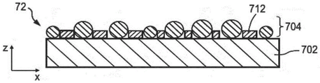
The particles may be deposited on the support layer via vertical colloidal deposition. The particles may form a single layer deposited on the surface of the support layer, and the scattering layer forms a corrugated undulating scattering surface on the support layer. The particles form a plurality of layers deposited on the surface of the support layer, each layer of the plurality of layers being in a plane substantially perpendicular to the direction of the received radiation in use.
The method may further comprise removing the particles after depositing the scattering material.
Also described is a method of forming a diffuser for receiving and transmitting radiation, the method comprising: depositing a plurality of particles on a surface of a support layer to form a mask; depositing a second material on the surface of the support layer over the mask to form a layer of the second material around the plurality of particles; removing at least some of the plurality of particles to form pits within the layer of the second material; depositing a scattering material into at least some of the pits within the second material to form scattering features within the layer of the second material.
Also described is a method of forming a diffuser for receiving and transmitting radiation, the method comprising: depositing a plurality of particles on a surface of a support layer to form a mask; depositing a second material on the surface of the support layer over the mask; selectively etching the surface of the support layer to form a plurality of structures on the surface of the support layer; depositing a scattering material onto the surface of the support layer, the scattering material formed over the plurality of structures to form a scattering layer; wherein the second material is a catalyst and the selectively etching comprises etching regions of the support layer in contact with the second material, or wherein the second material is a protective material and the selectively etching comprises etching regions of the support layer not in contact with the second material.
Also described herein is a method of forming a diffuser for receiving and transmitting radiation, the method comprising: depositing a plurality of particles onto a surface of a support layer such that the particles form a body that contacts the particles. The particles may be deposited from a dispersion of the particles in a liquid. The particles may be deposited to have a particle density such that a majority of the particles are in contact with one or more adjacent particles.
The depositing may include at least one of: vertical colloidal deposition, spin coating, and ink jet printing. Such a deposition method provides an easy diffuser fabrication method.
Depositing the plurality of particles may further include fusing the plurality of particles. The plurality of particles may be fused via the provision of heat and/or pressure. The plurality of particles may be fused using sintering.
The particles may include a binary mixture including a first material and a second material having a different refractive index than the first material. The first material may comprise molybdenum, ruthenium, niobium, rhodium, yttrium, or technetium. The second material may include silicon.
The method may further include forming another scattering layer on the diffuser. The further scattering layer may be formed according to the method of any of the examples described herein.
Forming a further scattering layer may comprise depositing an intermediate layer over the scattering layer and forming the further scattering layer on top of the intermediate layer. For example, the intermediate layer may be silicon or silicon nitride.
In any of the example methods for forming a diffuser described herein, the support layer may be formed on a carrier layer to support the support layer when forming the diffuser, and wherein the method further comprises removing the carrier layer once the first and second layers have been formed. The carrier layer may be, for example, silicon. For example, the carrier layer may be a standard silicon wafer of the type commonly used in semiconductor manufacturing.
Also described herein is a method of forming a diffuser for receiving and transmitting radiation, the method comprising producing a plurality of structures on a surface of a support layer of the diffuser, wherein the structures are arranged to produce a hologram upon receiving radiation at the surface. The radiation may be EUV radiation. A diffuser operable to produce a hologram may advantageously provide controlled diffusion of radiation in combination with minimal absorption of the radiation. Such a diffuser may have an increased lifetime compared to known diffusers, e.g. due to a reduced absorption of radiation.
The hologram may have an angular intensity distribution that is at least in a radially outer portion of the hologram as strong as compared to a central region of the hologram. The angular intensity distribution may have a similar intensity in the central region compared to the radially outer portion of the hologram. The angular intensity distribution may be a top hat distribution. The angular intensity distribution may have a lower intensity in the central region than in the radially outer portion of the hologram. The radially outer portion may be angularly spaced from the center of the hologram by at least 9 °. Such diffusers may have particular benefits in devices with high numerical apertures.
Photolithography may be used to create the plurality of structures. Each of the plurality of structures may have Is provided, wherein λ is the wavelength of the radiation that produces said hologram when received by the diffuser, and the holographic diffuser is provided with an effective refractive index neff.
The method may further include depositing a second substance into a plurality of voids distributed within the plurality of structures. The second substance has a thickness such that a combined thickness profile of the first substance and the second substance is substantially constant. That is, after providing the second substance, the surface of the diffuser operable to produce a hologram upon receiving radiation may be substantially smooth. The second substance may be a scattering substance. The real part of the refractive index of the second substance may be different from the real part of the refractive index of the first substance. Advantageously, the first and second substances having different real parts of their refractive indices may scatter radiation. The imaginary part of the refractive index of the second substance may be similar to the imaginary part of the refractive index of the first substance. Advantageously, the first and second substances having similar imaginary parts of the refractive indices of the first and second substances may reduce attenuation through the diffuser. The combined first and second substances act to reduce the relative difference in attenuation experienced by radiation traveling through the structure and the void.
The method may further include generating a thickness profile corresponding to a desired arrangement of a plurality of surface features, the desired arrangement based on a desired angular profile of the hologram. Generating the thickness profile may include numerical methods. Generating the thickness profile may include iteratively solving and/or performing calculations based on the optical relationship. The optical relationship may represent one or more of: attenuation, refractive index, scattering angle, layer thickness, phase shift. The thickness profile generation may include limits on maximum and/or minimum allowed thicknesses. The maximum and/or minimum allowed thicknesses may be based on manufacturing parameters. The maximum and/or minimum allowed thickness may be based on desired optical properties, such as attenuation.
Generating the thickness profile may include using a Gerchberg-Saxton algorithm. Generating the thickness profile may include using a modified version of the Gerchberg-Saxton algorithm.
Any of the example methods of forming a diffuser described herein may also include etching the support layer from a surface of the support layer opposite a surface of the support layer supporting the scattering layer.
Any of the example methods for forming a diffuser described herein may further include providing a cap layer at least partially covering the support layer and/or the scattering layer.
The method described herein may further comprise: once the plurality of nanoparticles have been deposited so as to form the nanoparticle layer supported by the support layer, the support layer is etched from a surface of the support layer opposite a surface of the support layer supporting the nanoparticle layer.
This back etching of the support layer allows for the use of a thicker, more stable support layer during the manufacture of the diffuser. Advantageously, this may prevent damage or even breakage of the support layer. Such a final etching step may be particularly beneficial for embodiments in which a colloid is used to deposit the nanoparticles, since such a final etching step may prevent capillary forces from braking the support layer. Once the nanoparticle layer has been formed, the thickness of such layer can be finalized using an etching process.
The method described herein may further comprise: providing a cover layer at least partially covering the support layer and/or the cap layer.
The term patterning device, as used herein, may also be referred to herein as a mask or a reticle, and the terms will be understood to be synonymous.
Drawings
Embodiments of the invention will now be described, by way of example only, with reference to the accompanying schematic drawings in which:
figure 1 depicts a lithographic system comprising a lithographic apparatus and a radiation source;
figure 2 is a schematic illustration of a reflective marker;
fig. 3A and 3B are schematic illustrations of a sensor device;
FIG. 4A depicts an intensity distribution of a bipolar illumination mode of the lithographic apparatus shown in FIG. 1;
FIG. 4B depicts an intensity distribution of a four-level illumination mode of the lithographic apparatus shown in FIG. 1;
fig. 5A to 5C schematically depict intermediate stages in an example process for manufacturing a transmissive diffuser;
6A-6C schematically depict intermediate stages in another example process for manufacturing a transmissive diffuser;
figures 7A to 7E schematically depict intermediate stages in another example process for manufacturing a transmissive diffuser;
figures 8A to 8D schematically depict intermediate stages in another example process for manufacturing a transmissive diffuser;
fig. 9A to 9E schematically depict intermediate stages in another example process for manufacturing a transmissive diffuser;
10A-10E schematically depict intermediate stages in another example process for manufacturing a transmissive diffuser;
11A-11C schematically depict intermediate stages in another example process for manufacturing a transmissive diffuser;
figure 12 schematically illustrates an EUV diffuser;
figure 13 shows a plot of the extinction coefficient k for EUV radiation versus the magnitude of (1-n) for EUV radiation for some materials;
fig. 14A to 14C schematically depict intermediate stages in another example process for manufacturing a transmissive diffuser;
fig. 15A illustrates a height map of an example diffuser manufactured according to the process of fig. 14A-14C;
15B and 15C depict the scattering angle of the plane wave of the radiation incident on the diffuser of FIG. 15A;
fig. 16A and 16B schematically depict an intermediate stage in another example process for manufacturing a transmissive diffuser;
FIG. 17 illustrates the properties of an example diffuser manufactured according to the process of FIGS. 16A and 16B;
FIG. 18 illustrates the properties of an example diffuser manufactured according to the process of FIGS. 16A and 16B;
FIG. 19 illustrates the properties of an example diffuser manufactured according to the process of FIGS. 16A and 16B; and
fig. 20 illustrates the properties of an example diffuser manufactured according to the process of fig. 16A and 16B.
Detailed Description
Fig. 1 shows a lithographic system comprising a radiation source SO and a lithographic apparatus LA. The radiation source SO is configured to generate an EUV radiation beam B and to supply the EUV radiation beam B to the lithographic apparatus LA. The lithographic apparatus LA comprises an illumination system IL, a support structure MT configured to support a patterning device MA (e.g. a mask), a projection system PS, and a substrate table WT configured to support a substrate W.
The illumination system IL is configured to condition the EUV radiation beam B before it is incident on the patterning device MA. In addition, the illumination system IL may comprise a facet field mirror device 10 and a facet pupil mirror device 11. The faceted field mirror device 10 and the faceted pupil mirror device 11 together provide the EUV radiation beam B with a desired cross-sectional shape and a desired intensity distribution. The illumination system IL may also comprise other mirrors or devices in addition to or instead of the facet field mirror device 10 and the facet pupil mirror device 11.
After being so conditioned, the EUV radiation beam B interacts with the patterning device MA. Due to this interaction, a patterned beam B' of EUV radiation is produced. The projection system PS is configured to project the patterned EUV radiation beam B' onto a substrate W. For this purpose, the projection system PS may comprise a plurality of mirrors 13, 14 configured to project the patterned beam B' of EUV radiation onto a substrate W held by the substrate table WT. The projection system PS may apply a reduction factor to the patterned EUV radiation beam B', thus forming an image having smaller features than corresponding features on the patterning device MA. For example, a reduction factor of 4 or 8 may be applied. Although the projection system PS is illustrated as having only two mirrors 13, 14 in fig. 1, the projection system PS may include a different number of mirrors (e.g., six or eight mirrors).
The substrate W may include a previously formed pattern. In such cases, the lithographic apparatus LA aligns an image formed by the patterned EUV radiation beam B' with a pattern previously formed on the substrate W.
A relative vacuum, i.e., a small amount of gas (e.g., hydrogen) at a pressure substantially lower than atmospheric pressure, may be provided in the radiation source SO, in the illumination system IL, and/or in the projection system PS.
The radiation source SO may be a Laser Produced Plasma (LPP) source, a Discharge Produced Plasma (DPP) source, a Free Electron Laser (FEL), or any other radiation source capable of producing EUV radiation.
The lithographic apparatus may, for example, be used in a scanning mode, in which the support structure (e.g. mask table) MT and the substrate table WT are scanned synchronously (i.e. dynamic exposure) while a pattern imparted to the radiation beam is projected onto the substrate W. The velocity and direction of the substrate table WT relative to the support structure (e.g. mask table) MT may be determined by the demagnification and image reversal characteristics of the projection system PS. The patterned beam of radiation incident on the substrate W may comprise a band of radiation. The band of radiation may be referred to as an exposure slit. During a scanning exposure, movement of the substrate table WT and support structure MT may cause an exposure slit to travel over an exposure field of the substrate W.
As already described above, the lithographic apparatus may be used to expose portions of a substrate W to form a pattern on the substrate W. To improve the accuracy of transferring a desired pattern to the substrate W, one or more properties of the lithographic apparatus LA may be measured. Such properties may be measured periodically, for example before and/or after exposure of each substrate W, or may be measured less frequently, for example as part of a calibration process. Examples of properties of the lithographic apparatus LA that may be measured include relative alignment of components of the lithographic apparatus LA and/or aberrations of components of the lithographic apparatus. For example, measurements may be made to determine the relative alignment of the support structure MT supporting the patterning device MA and the substrate table WT supporting the substrate W. Determining the relative alignment of the support structure MT and the substrate table WT helps to project the patterned radiation beam onto a desired portion of the substrate W. This may be particularly important when projecting patterned radiation onto a substrate W comprising portions that have been exposed to radiation in order to improve alignment of the patterned radiation with previously exposed areas. Additionally or alternatively, measurements may be made to determine the deformation of the patterning device MA.
Additionally or alternatively, measurements may be made to determine optical aberrations of the projection system PS. Optical aberrations are deviations of the performance of the optical system from paraxial optics and can cause blurring or distortion of the pattern exposed at the substrate W. Aberrations of the projection system PS may be adjusted and/or accounted for in order to increase the accuracy with which a desired pattern is formed on the substrate W.
Measurements, such as alignment and aberration measurements described above, may be performed by illuminating the reflective marker 17 (as schematically shown in fig. 1) with radiation. In an alternative arrangement, transmissive markers may be used. A marker is a reflective feature that appears in an image produced by an optical system when the marker is placed in the field of view of the optical system. The reflective markers described herein are suitable for use as reference points and/or as a measure of the properties of the image formed by the optical system. For example, radiation reflected from the reflective marker may be used to determine alignment of one or more components and/or optical aberrations of one or more components.
In the embodiment shown in fig. 1, the reflective marker 17 forms part of the patterning device MA. One or more markers 17 may be provided on the patterning device MA for performing lithographic exposure. The marking 17 may be positioned outside a patterned area of the patterning device MA, which is irradiated with radiation during lithographic exposure. In some embodiments, one or more markers 17 may additionally or alternatively be provided on the support structure MT. For example, a piece of dedicated hardware (often referred to as a fiducial piece) may be provided on the support structure MT. The reference piece may include one or more identifiers. For the purposes of this specification, a reference is considered to be an example of a patterning device. In some embodiments, a patterning device MA, which is specifically designed to measure one or more properties of the lithographic apparatus LA, may be placed on the support structure MT in order to perform a measurement process. The patterning device MA may comprise one or more markers 17 for performing the illumination as part of the measurement process.
In the embodiment shown in fig. 1, the lithographic apparatus LA is an EUV lithographic apparatus and thus uses a reflective patterning device MA. The marking 17 is thus a reflective marking 17. The configuration of the identifier 17 may depend on the properties of the measurements to be made using the identifier 17. The marking may, for example, comprise one or more reflective pinhole features comprising a reflective area surrounded by an absorbing area, a reflection line feature, an arrangement of a plurality of reflection line features, and/or a reflection grating structure such as a reflective diffraction grating.
To measure one or more properties of the lithographic apparatus LA, a sensor device 19 (shown schematically in fig. 1) is provided to measure the radiation output from the projection system PS. As shown in fig. 1, the sensor device 19 may, for example, be provided on the substrate table WT. To perform a measurement process, the support structure MT may be positioned such that the markers 17 on the patterning device MA are irradiated with radiation. The substrate table WT may be positioned such that radiation reflected from the markers is projected by the projection system PS onto the sensor device 19. The sensor device 19 is in communication with a controller CN, which may determine one or more properties of the lithographic apparatus LA from measurements made by the sensor device 19. In some embodiments, a plurality of markers 17 and/or sensor devices 19 may be provided, and properties of the lithographic apparatus LA may be measured at a plurality of different field points (i.e. locations in the field or object plane of the projection system PS).
As described above, in some embodiments, radiation reflected from the markers may be used to determine the relative alignment of components of the lithographic apparatus LA. In such embodiments, the marker 17 may comprise features that, when illuminated with radiation, apply alignment features to the radiation. The features may for example comprise one or more reflective patterns in the form of grating structures.
The position of the alignment feature in the radiation beam B may be measured by a sensor device 19 located at the level of the substrate W (e.g. on the substrate table WT as shown in fig. 1). The sensor device 19 may be operable to detect the position of the alignment feature in the radiation incident on the sensor device 19. This may allow the substrate table WT to be aligned relative to a mark on the patterning device MA to be determined. Knowing the relative alignment of the patterning device MA and the substrate table WT, the patterning device MA and the substrate table WT can be moved relative to each other to form a pattern at a desired location on the substrate W (using the patterned radiation beam B reflected from the patterning device MA). A separate measurement process may be used to determine the position of the substrate W on the substrate table.
As described further above, in some embodiments, the patterning device MA may be provided with one or more markers 17 that may be used to measure aberrations of the projection system PS. Similar to the alignment measurements described above, the aberrations may be detected by measuring the radiation reflected from the marks 17 with a sensor device 19 located at or near the substrate table WT. One or more markers 17 on the patterning device MA may be irradiated with EUV radiation by the illumination system IL. The radiation reflected from the one or more markers is projected by a projection system PS onto an image plane of the projection system PS. One or more sensor devices 19 are positioned at or near the image plane (e.g. on the substrate table WT as shown in fig. 1) and may measure the projected radiation in order to determine aberrations of the projection system PS. An embodiment of the markers 17 and the sensor device 19 that can be used for determining the aberrations of the projection system PS will now be described with reference to fig. 2 and 3.
Fig. 2 is a schematic view of a logo 17 that may form part of a patterning device MA according to an embodiment of the invention. A cartesian coordinate system is also shown in fig. 2. The y-direction may represent a scanning direction of the lithographic apparatus. That is, during a scanning exposure, movement of the substrate table WT and support structure MT may be such that the patterning device MA is scanned in the y-direction relative to the substrate W. The indicia 17 generally lie in the x-y plane. That is, the indicia generally extend in a direction perpendicular to the z-direction. While reference is made to a logo that generally lies in a plane, it will be understood that the logo is not completely constrained/limited to a plane. That is, portions of the indicia may extend out of the plane in which the indicia generally lie. As will be explained further below, the marker may comprise a diffraction grating. The diffraction grating may comprise a three-dimensional structure comprising portions that are not completely in plane but instead extend out of plane.
The label 17 shown in fig. 2 comprises a first part 17a and a second part 17 b. Both the first and second portions comprise a reflective diffraction grating comprising a periodic grating structure. The grating structure extends in a grating direction. The first portion 17a comprises a diffraction grating extending in a first grating direction, which is indicated in fig. 2 as the u-direction. The second portion 17b comprises a diffraction grating extending in a second grating direction, which is indicated in fig. 2 as the v-direction. In the embodiment of fig. 2, both the u-direction and the v-direction are aligned at approximately 45 ° with respect to both the x-and y-directions and are substantially perpendicular to each other. The first portion 17a and the second portion 17b of the marking 17 may be irradiated with radiation at the same time or at different times.
Although the embodiment shown in fig. 2 includes a first portion 17a and a second portion 17b that include diffraction gratings oriented in a perpendicular grating direction, in other embodiments, the indicia 17 may be provided in other forms. For example, the indicia 17 may comprise reflective and absorptive regions arranged to form a checkerboard pattern. In some embodiments, the indicia 17 may comprise an array of pinhole features. The reflective pinhole feature may comprise an area of reflective material surrounded by an absorbing material.
When the first portion 17a and/or the second portion 17b of the marking is illuminated by radiation, a plurality of diffraction orders are reflected from the marking. At least a portion of the reflected diffraction order enters the projection system PS. The projection system PS forms an image of the marking 17 on the sensor device 19. Fig. 3A and 3B are schematic views of the sensor device 19. Fig. 3A is a side view and fig. 3B is a top view of the sensor apparatus. Cartesian coordinates are also shown in FIGS. 3A and 3B.
The cartesian coordinate systems used in fig. 2, 3A and 3B are intended to be the coordinate system of the radiation propagating through the lithographic apparatus. At each reflective optical element, the z-direction is defined as the direction perpendicular to the optical element. That is, in fig. 2, the z-direction is perpendicular to the x-y plane in which patterning device MA and mark 17 generally extend. In fig. 3A and 3B, the z-direction is perpendicular to the x-y plane in which the diffraction grating 19 and radiation sensor 23 generally extend. The y-direction denotes a scan direction in which the support structure MT and/or the substrate table WT are scanned relative to each other during a scanning exposure. The x direction denotes a non-scanning direction perpendicular to the scanning direction. It will be appreciated (e.g. from fig. 1) that in a lithographic apparatus the z-direction at the patterning device MA is not aligned with the z-direction at the substrate W. As explained above, the z-direction is defined as being perpendicular to the optical elements at each optical element in the lithographic apparatus.
The sensor device 19 comprises a transmission type diffraction grating 21 and a radiation sensor 23. At least some of the radiation 25 output from the projection system PS passes through the diffraction grating 21 and is incident on a radiation sensor 23. The diffraction grating 21 is shown in more detail in figure 3B and comprises a checkerboard diffraction grating. The areas of the diffraction grating 21 shown shaded black in fig. 3B represent areas of the diffraction grating 21 that are configured to be substantially opaque to incident radiation. The unshaded regions of the diffraction grating 21 shown in fig. 3B represent regions configured to transmit radiation. For ease of illustration, the opaque and transmissive regions of diffraction grating 21 are not shown to scale in FIG. 3B. For example, in practice, the proportion of the diffraction grating features relative to the size of the diffraction grating itself may be less than that indicated in figure 3B.
The diffraction grating 21 shown in fig. 3B is depicted as having a checkerboard configuration with square transmissive areas and opaque areas. In practice, however, it may be difficult or impossible to manufacture a transmissive diffraction grating comprising completely square transmissive regions and opaque regions. The transmissive region and/or the opaque region may thus have a cross-sectional shape other than a perfect square. For example, the transmissive region and/or the opaque region may have a cross-sectional shape that includes a square (or more generally a rectangle) with rounded corners, i.e., rounded processed corners. In some embodiments, the transmissive region and/or the opaque region may have a substantially circular or elliptical cross-sectional shape. In some embodiments, the diffraction grating 21 may comprise an array of pinholes formed in an optically opaque material.
The radiation sensor 23 is configured to detect a spatial intensity distribution of radiation incident on the radiation detector 23. The radiation detector 23 may, for example, comprise an array of individual detector elements. For example, the radiation detector 23 may comprise a CCD or CMOS array. During the process for determining aberrations, the support structure MT may be positioned such that the marking 17 is irradiated with radiation from the illumination system IL. The substrate table WT may be positioned such that radiation reflected from the markers is projected by the projection system PS onto the sensor device 19.
As described above, a plurality of diffraction orders are formed at the mark 17. Further diffraction of the radiation occurs at the diffraction grating 21. The interaction between the diffraction order formed at indicia 17 and the diffraction pattern formed at diffraction grating 21 produces an interference pattern formed on radiation detector 23. The interference pattern is related to the derivative of the phase of the wavefront that has propagated through the projection system. Thus, the interference pattern may be used to determine aberrations of the projection system PS.
As described above, the first and second portions of the logo 17 comprise diffraction gratings aligned perpendicular to each other. Radiation reflected from the first portion 17a of the marker 17 may provide information about the gradient of the wavefront along the first direction. Radiation reflected from the identified second portion 17b may provide information about the gradient of the wavefront along a second direction, which is perpendicular to the first direction. In some embodiments, the first and second portions of the marker may be illuminated at different times. For example, a first portion 17a of the marker 17 may be illuminated at a first time to derive information relating to the gradient of the wavefront in a first direction, and a second portion 17b of the marker 17 may be illuminated at a second time to derive information relating to the gradient of the wavefront in a second direction.
In some embodiments, patterning device MA and/or sensor apparatus 19 may be scanned sequentially and/or stepped in two perpendicular directions. For example, the patterning device MA and/or the sensor arrangement 19 may be stepped with respect to each other in the u-direction and the v-direction. While the patterning device MA and/or the sensor device 19 may be stepped in the u-direction, a second part 17b of the marking 17 is illuminated; and the first part 17a of the marking 17 is illuminated while the patterning device MA and/or the sensor device 19 may be stepped in the v-direction. That is, the patterning device MA and/or the sensor apparatus 19 may be stepped in a direction perpendicular to the grating direction of the illuminated diffraction grating.
The patterning device MA and/or the sensor apparatus 19 may be stepped by a distance corresponding to a fraction of the grating period of the diffraction grating. Measurements taken at different step positions may be analyzed to derive information about the wavefront in the step direction. For example, the phase of the first harmonic of the measured signal may contain information about the derivative of the wavefront in the stepping direction. Thus, stepping the patterning device MA and/or the sensor apparatus 19 in both the u-direction and the v-direction (which are perpendicular to each other) allows deriving information about the wavefront in both perpendicular directions, thereby allowing reconstructing the complete wavefront.
In addition to the stepping of the patterning device MA and/or the sensor device 19 in a direction perpendicular to the grating direction of the diffraction grating being illuminated (as described above), the patterning device MA and/or the sensor device 19 may also be scanned relative to each other. The scanning of the patterning device MA and/or the sensor device 19 may be performed in a direction parallel to the grating direction of the diffraction grating being illuminated. For example, a first portion 17a of the marking 17 is illuminated while the patterning device MA and/or the sensor device 19 may be scanned in the u-direction; and a second part 17a of the marking 17 is illuminated while the patterning device MA and/or the sensor device 19 may be scanned in the v-direction. Scanning the patterning device MA and/or the sensor apparatus 19 in a direction parallel to the grating direction of the diffraction grating being illuminated allows averaging of the measurements across the entire diffraction grating, thereby taking into account any variation in the diffraction grating in the scanning direction. The scanning of the patterning device MA and/or the sensor device 19 may be performed at different times than the stepping of the patterning device MA and/or the sensor device 19 described above.
As described above, the diffraction grating 21 forming part of the sensor device 19 is configured in the form of a checkerboard. This may allow the sensor device 19 to be used during the determination of the phase change of the wavefront in both the u-direction and the v-direction. The arrangement of the diffraction gratings forming the marking 17 and the sensor device 19 is presented only as an exemplary embodiment. It will be appreciated that a variety of different arrangements may be used in order to determine the wavefront variation.
In some embodiments, the marker 19 and/or the sensor device 19 may comprise components other than a diffraction grating. For example, in some embodiments, the marker 17 and/or the sensor device 19 may comprise a single slit or one or more pinhole features through which at least a portion of the radiation beam may propagate. In the case of the marker 17, the pinhole feature may comprise a portion of reflective material surrounded by absorbing material, such that radiation is reflected from only a smaller portion of the marker. The single slit feature may be in the form of a single strip of reflective material surrounded by an absorptive material. The pinhole feature and/or the single slit feature at the sensor device 19 may be a transmission feature. In general, the marking 17 may be any feature that imparts to the radiation beam a feature that may be used as a reference point or to determine a measurement of the radiation beam.
Although in the above described embodiment a single marker 17 and sensor device 19 is provided, in other embodiments a plurality of markers 17 and sensor devices 19 may be provided in order to measure the phase change of the wavefront at different field points. In general, any number and configuration of identification and sensor devices 19 may be used to provide information related to the phase change of the wavefront.
The controller CN (as shown in fig. 1) receives the results of the measurements made at the sensor device 19 and determines the aberrations of the projection system PS from the results of the measurements. The controller may also be configured to control one or more components of the lithographic apparatus LA. For example, the controller CN may control a positioning device operable to move the substrate table WT and/or the support structure MT relative to each other. The controller CN may control an adjusting means PA for adjusting components of the projection system PS. For example, the adjusting means PA may adjust elements of the projection system PS in order to correct aberrations determined by the controller CN.
The projection system PS includes a plurality of reflective lens elements 13, 14 and an adjusting device PA for adjusting the lens elements 13, 14 so as to correct aberrations. To achieve this correction, the adjustment device PA may be operable to manipulate the reflective lens element within the projection system PS in one or more different ways. The adjustment means PA may be operable to make any combination of: displacing one or more lens elements; tilting one or more lens elements; and/or deforming one or more lens elements.
The projection system PS has an optical transfer function that may be non-uniform, which may affect the pattern imaged on the substrate W. For unpolarized radiation, these effects can be very well described by two scalar maps or graphs, which describe the transmission (apodization) and relative phase (aberration) of the radiation exiting the projection system PS as a function of position in a pupil plane of the projection system PS. These scalar maps, which may be referred to as transmission maps and relative phase maps, may be expressed as a linear combination of the complete set of basis functions. It will be understood that the terms "transmission map" and "relative intensity map" are synonymous and that a transmission map may alternatively be referred to as a relative intensity map. A particularly convenient set of basis functions for expressing these scalar mappings is the Zernike (Zernike) polynomials which form a set of orthogonal polynomials defined on a unit circle. The determination of each scalar map may involve determining coefficients in such an expansion. Since the zernike polynomials are orthogonal on a unit circle, the zernike coefficients can be determined by calculating the inner product of the measured scalar map with each zernike polynomial in turn and dividing this inner product by the square of the norm of the zernike polynomial.
The transmission mapping and the relative phase mapping are field and system dependent. That is, typically, each projection system PS will have a different zernike expansion for each field point (i.e., for each spatial location in the image plane of the projection system PS).
Determining the aberrations of the projection system PS may comprise fitting the wavefront measurements made by the sensor device 19 to zernike polynomials to obtain zernike coefficients. Different zernike coefficients may provide information about different forms of aberrations caused by the projection system PS. The zernike coefficients may be determined independently at different locations (i.e., at different field points) in the x and/or y directions.
Different zernike coefficients may provide information about different forms of aberrations caused by the projection system PS. Typically, a zernike polynomial is considered to include a plurality of orders, each order having an associated zernike coefficient. The order and coefficients may be labeled with an index, commonly referred to as the Noll (Noll) index. A zernike coefficient with a noral index of 1 may be referred to as a first zernike coefficient, a zernike coefficient with a noral index of 2 may be referred to as a second zernike coefficient, and so on.
The first zernike coefficient is related to the average of the measured wavefronts (which may be referred to as the "piston"). The first zernike coefficients may not be related to the performance of the projection system PS and, as such, the first zernike coefficients may not be determined using the methods described herein. The second zernike coefficient is related to the tilt of the measured wavefront in the x-direction. The tilt of the wavefront in the x-direction is equivalent to the placement in the x-direction. The third zernike coefficient is related to the tilt of the measured wavefront in the y-direction. The tilt of the wavefront in the y-direction is equivalent to the placement in the y-direction. The fourth Zernike coefficient is related to the defocus of the measured wavefront. The fourth zernike coefficient is equivalent to the placement in the z direction. Higher order zernike coefficients are associated with other forms of aberrations such as astigmatism, coma, spherical aberration and other effects.
Throughout this specification, the term "aberration" is intended to include all forms of deviation of a wavefront from a perfectly spherical wavefront. That is, the term "aberration" may be related to the placement of the image (e.g., the second, third, and fourth zernike coefficients) and/or to higher order aberrations, such as aberrations related to zernike coefficients having a nori index of 5 or greater.
As described in detail above, one or more reflection type markers 17 may be used to determine alignment and/or aberrations of components of the lithographic apparatus LA. In some embodiments, a separate marker 17 may be used to determine the alignment of the component with the marker used to determine the aberration. For example, a patterning device MA suitable for use in a lithographic exposure process may have one or more marks outside the patterned area suitable for use in the lithographic exposure process. The one or more markers may be suitable for determining the alignment of the patterning device MA with respect to the substrate table WT.
One or more markers 17 suitable for determining aberrations may be provided on the measurement patterning device separate from the patterning device MA (e.g. reticle) used to perform the lithographic exposure. For the purpose of performing aberration measurements, the measurement patterning device MA may, for example, be arranged on the support structure MT. The measurement patterning device MA may comprise other features suitable for determining other properties of the projection system PS. For example, the measurement patterning device may additionally comprise a marker adapted to determine the alignment of the measurement patterning device with respect to the substrate table WT.
In some embodiments, the same identification may be used to determine both alignment and aberration. For example, one or more markers in the form of reflective grating structures (e.g., diffraction gratings) may be used to determine both alignment and aberration. In some embodiments, the same set of measurements may be used to determine both alignment and aberration simultaneously.
References herein to patterning device MA should be construed to include any device that includes one or more features configured to modify radiation. The patterning device MA may, for example, be provided with a pattern for use during lithographic exposure (e.g. the patterning device may be a reticle). Additionally or alternatively, the patterning device may be provided with one or more markers for measuring the process. Generally, the patterning device MA is a removable part that is placed on the support structure MT in order to perform a certain process (e.g., to perform a lithographic exposure and/or to perform one or more measurement processes). However, in some embodiments, the lithographic apparatus LA itself may be provided with one or more patterned features. For example, the support structure MT may be provided with one or more patterned features (e.g. markers) for use in a measurement process. For example, the support structure MT may be provided with one or more fiducials including one or more markers. In such embodiments, the support structure MT may itself be considered as an example of a patterning device, since the support structure MT is provided with one or more features configured to modify the radiation. References herein to a patterning device comprising a reflective marking should not be construed as limited to a removable patterning device, but rather should be construed to encompass any device having a reflective marking disposed thereon.
Referring to fig. 1, the patterning device MA may be considered to be disposed in the object plane of the projection system PS and the substrate W may be considered to be disposed in the image plane of the projection system PS. In the context of such a lithographic apparatus, the object plane of the projection system PL in which the patterning device MA is arranged, the image plane of the projection system PL in which the substrate W is arranged and any plane conjugate thereto may be referred to as the field plane of the lithographic apparatus. It will be appreciated that within an optical system (e.g. a lithographic apparatus), two planes are conjugate if each point within the first plane P is imaged onto a point of the second plane P'.
It will be understood that the lithographic apparatus LA comprises optics (i.e. focusing and/or diverging optics) having optical power or optical power in order to form an image in an image plane of the object in the object plane. In such an optical system, a pupil plane can be defined between each pair of field planes as a fourier transform plane of the preceding field plane and the successive field plane. The distribution of the electric field in each such pupil plane is related to the fourier transform of the object disposed in the previous field plane. It will be appreciated that the quality of such pupil planes will depend on the optical design of the system and that such pupil planes may even be curved. This applies to consider two such pupil planes: a pupil plane of the illumination system and a pupil plane of the projection system. Pupil plane of an illumination system and pupil plane of a projection systemThe facets (and any other pupil planes) are planes that are conjugate to each other. Radiation in a pupil plane PP of the illumination systemILAn intensity (or equivalently, electric field strength) distribution in (a) may be referred to as an illumination mode or pupil filling and characterizes the angular distribution of the light cone at the patterning device MA (i.e. in the object plane). Similarly, the radiation is in the pupil plane PP of the projection systemILThe intensity (or equivalently, the electric field strength) distribution in (c) characterizes the angular distribution of the light cone at the wafer level (i.e., in the image plane).
The illumination system IL may change the intensity distribution of the beam in a pupil plane of the illumination system. This can be achieved by appropriately configuring the facet field mirror device 10 and the facet pupil mirror device 11.
During exposure of the substrate W, the illumination system IL and the projection system PS are used to form a (diffraction limited) image of the object-level patterning device MA on an image-level substrate W (e.g. a resist-coated silicon wafer). During such exposure, for the illumination mode, it may be desirable to use a local illumination mode. For example, it may be desirable to use a multipole (e.g., dipole or quadrupole) illumination mode in which the PP is illuminated in the illumination systemILOnly a limited number (e.g. two or four) of discrete polar regions receive radiation in the pupil plane of (a). Two examples of such illumination modes are shown in fig. 4A and 4B. For example, the illumination mode may be a dipole distribution 30 as shown in fig. 4A or a quadrupole distribution 32 as shown in fig. 4B. Also shown in fig. 4A and 4B is a ring 34, the ring 34 representing a limit (which represents the numerical aperture NA, or sine of the maximum angle that can be captured by the projection system PS) that can be physically captured by the projection system PS and imaged onto the image plane. The ring 34 has a radius σ of 1 in coordinates normalized by the numerical aperture NA of the projection system PS. The dipole distribution 30 includes two diametrically opposed polar regions 36 in which the intensity is non-zero 36. Quadrupole distribution 32 includes a first dipole distribution similar to the dipole distribution shown in fig. 4A and a second dipole distribution rotated by pi/2 radians relative to the first dipole distribution but otherwise consistent with the first dipole distribution. Thus, the quadrupole distribution 32 comprises four pole regions 34, whereThe intensity in the field 34 is non-zero.
When the lithographic apparatus is not exposing the substrate W, one of more reflective markers provided on the patterning device MA may be used in a measurement process, for example to determine alignment and/or aberrations associated with the lithographic apparatus LA. When using reflections from markers to measure alignment and/or aberrations, it may be desirable for radiation reflected from the markers to fill a larger portion of the pupil of the projection system PS. To achieve this filling, in principle, the illumination system IL may be reconfigured to fill the pupil plane of the illumination system (and hence also the entrance pupil of the projection system). However, more time may be spent for this purpose (and for returning to the exposure illumination mode before the next exposure) than is required for such an on-line measurement or on-line measurement. It is therefore known to provide a diffuser during such measurements, which diffuser is arranged to increase the angular spread, i.e. angular spread, of the radiation scattered from the object-level patterning device in order to increase the proportion of the entrance pupil of the projection system PS that is filled with radiation.
Such a diffuser may be placed in the path of the radiation beam during these metrology measurements, but not during exposure of the substrate W. This allows the EUV lithographic apparatus to be operable to perform semi-continuous on-line metrology, i.e. in-line metrology, which may then be used to maintain optimal dynamic settings of the projection system PS, support structure MT and substrate table WT. In addition, such a measurement system may be used to align patterning device MA with substrate W prior to exposing the substrate W.
At the object level, some existing measurement systems use a combined diffuser and patterning device (e.g., a one-dimensional diffraction grating). One arrangement uses a three-dimensional structure mounted on a support structure MT, which includes a recessed diffuser and a grating diaphragm disposed in two different planes. The EUV radiation beam B exits the illumination system IL for radiation, reflects from a recessed diffuser (which increases the angular spread of the radiation), and then passes after reflection through a grating membrane (which scatters the radiation, some of which is captured by the projection system). Such a three-dimensional arrangement cannot be formed on the reticle and thus on the fiducials.
Another arrangement uses a reflective object, a combined diffuser and patterning device, as described in WO 2017/207512. This arrangement is in the form of a multilayer reflective stack arranged to preferentially reflect EUV radiation, the arrangement being applied with a pattern of EUV absorbing material (e.g. a diffraction grating). Each layer in the multilayer reflective stack is provided with a surface roughness such that the reflected radiation is diffused. However, while in principle such patterning devices may be provided on a reticle, it is significantly more complicated to manufacture patterning devices having such built-in surface roughness. Thus, in practice, such patterning device is more likely to be formed on a reference member.
Embodiments of the present invention relate to novel diffusers, particularly suitable for use with EUV measurement systems within EUV lithographic apparatus of the type discussed above, and methods for their preparation.
Fig. 5A to 5C (collectively, fig. 5) schematically show stages in a method of preparing a diffuser according to a first example. The diffuser may be constructed from multiple layers, referred to herein as a stack. An intermediate stack of layers in one example process for creating a diffuser is depicted in cross-section in fig. 5A-5C. Referring to fig. 5A, the first intermediate laminate 50 includes a layer of support material 502. For example, the support material may include silicon nitride (SiN), silicon, molybdenum silicide (MoSi)2). The layer of support material 502 may have a thickness of about 10nm to 60 nm. In some embodiments, the support material is a material having a refractive index close to 1 for EUV radiation and a relatively low absorption coefficient for EUV radiation. For such embodiments, the support material may be considered to be relatively optically neutral to EUV radiation. The layer of support material 502 is formed on a carrier layer 504 that may be used to support the layer of support material 502 while forming the diffuser. For example, the support layer 504 may be formed of silicon, silicon nitride (SiN), porous silicon (pSi), or molybdenum silicide (MoSi). The carrier layer 504 may for example beSuch as any thickness suitable to provide adequate support during manufacture, and in some arrangements, may have a thickness of about 100 to 500 μm. For example, the carrier layer may be a standard silicon wafer. Alternatively, the carrier layer 504 and the support layer 502 may be provided by a single layer of the same material.
A layer of scattering material 506 is disposed on the support layer 502. The scattering material may be, for example, a substance such as molybdenum, ruthenium, or niobium, but may be other suitable scattering materials, as discussed in further detail below. Depending on the particular scattering material, the layer 506 of scattering material may, for example, have a thickness (in the depicted z-direction) between approximately 50nm and 400 nm.
Another layer 508 of another different metal is deposited on top of the intermediate stack 50 to form a second intermediate stack 52. For example, the other metal may be zinc (Zn). The layers 506 and 508 are treated to form an alloy layer (not shown) comprising an alloy of the scattering metal and another metal, such as a molybdenum-zinc alloy. The scattering material 506 provides a first component of the alloy, while the other metal 508 provides a second component of the alloy. For example, the layers 506, 508 may be annealed. The anneal may be performed, for example, at 400 degrees. The annealing may be performed in a protective gas environment. For example, the annealing may be performed in the presence of an inert gas such as argon.
The resulting alloy layer is subjected to a dealloying, i.e., dealloying, process to selectively corrode the second component of the alloy. For example, where the second component is zinc, dealloying, i.e., dealloying, comprises a dezincing process. Dealloying, i.e. dealloying, may be performed by any suitable method. For example, dealloying, i.e., dealloying, can include selectively dissolving zinc by immersion in an acid (such as nitric acid).
After the dealloying, i.e., dealloying, process, an intermediate stack 54 is provided that includes a porous scattering layer 510 on a support layer 502. The scattering layer 510 may be considered as a scattering substance having a plurality of voids distributed therein. The method may further include etching the support layer 504 from a surface opposite to a surface of the support layer supporting the porous scattering layer 510. In the case where the carrier layer 502 and the support layer 504 are separate, i.e., separate, layers, the carrier layer 502 may provide an etch stop during this back side etching process. This back etching of the carrier layer 504 allows for the use of a thicker, more stable carrier 502 and support layer 504 during fabrication. Advantageously, this may prevent the support layer 504 from being damaged or even broken.
Alternatively, the porous scattering layer 510 may contain another substance located within the plurality of pores (or voids). For example, the plurality of pores of the porous scattering layer 510 may be filled with an inert gas. Alternatively, the plurality of pores of the porous scattering layer 510 may be filled with vacuum. For example, where the scattering layer 510 is subsequently capped (discussed in more detail below), the capping may be performed in an atmosphere of an inert gas, or in a vacuum. Alternatively, the porous scattering layer 510 may be infiltrated (by any suitable process, such as, for example, ALD, CVD, or sputtering) with a material that is optically significantly different (e.g., a material that is relatively optically neutral to EUV radiation, such as a material having a refractive index of 1 or approximately close to 1). Such penetration or wetting of the porous scattering layer 510 may be beneficial for protection from degradation, protection of structural integrity, allowing for thermal diffusion.
Although in practice the diffuser is likely to comprise a plurality of layers, such as a scattering layer and a support layer, the term diffuser herein may also refer to a scattering layer only (i.e. a layer configured to diffuse incident radiation).
Fig. 6A-6C (collectively, fig. 6) depict another example process for manufacturing a diffuser suitable for EUV radiation. An intermediate stack of layers in the example process is depicted in cross-section in fig. 6A-6C. Referring to fig. 6A, the first intermediate laminate 60 includes a support layer 602 and a carrier layer 604. The support layer 602 and carrier layer 604 may be as described above in connection with the support layer 502 and carrier layer 504 of fig. 5A-5C.
The intermediate laminate 60 further includes a porous layer 606, the porous layer 606 being formed from a material that has been processed to form a structure. For example, the porous layer 606 may comprise silicon or porous silicon. The process used to create the porous layer 606 may include, for example, selective etching (e.g., metal assisted chemical etching, anodization, selective leaching/leaching).
A scattering material is deposited onto the porous layer 602 to form the second intermediate laminate 62 such that the scattering material at least partially occupies the plurality of pores (or voids) within the porous layer 602 to thereby form the scattering layer 608. The scattering layer 604 may have a thickness of approximately between 50nm and 1000nm, depending on the scattering material used. The scattering layer 604 may be considered to provide a first substance having voids distributed therein, at least some of which are filled with a scattering substance.
As described with respect to the previous example process, the method may further comprise etching the carrier layer 604 from a surface opposite to that supporting the scattering layer 604 to provide a further stack 64 (which may be a final stack or may be a further intermediate stack). It should be appreciated that in other examples discussed below, although the carrier layer is not depicted, the carrier layer may be provided and may be etched after the scattering layer has been provided on the support structure.
In addition, in all examples described herein, additional layers may be provided in addition to those shown in fig. 5 and 6. For example, referring to fig. 5 as an example, another layer may be disposed between the support layer 502 and the scattering layer 510 or between the support layer 504 and the support layer 502. The additional layer may be beneficial to provide additional protection of the scattering layer during use, in particular from particles present inside the lithographic apparatus. Similarly, an additional (or "cap") layer may be disposed on top of the scattering layer 510 for the same purpose. Such an additional layer may have a thickness of about 10 nm. This additional layer formed forms a metal oxide or metal nitrate. For example, the additional layer may be provided from silicon nitride or molybdenum silicide.
Fig. 7A-7E (collectively, fig. 7) depict another example process for manufacturing a diffuser suitable for EUV radiation. In the example of fig. 7, a non-uniform layer of scattering material is deposited on a random or quasi-random arrangement of a plurality of structures (such as pillars on a surface of a support layer or holes in a surface of a support layer). The structures may be provided according to any suitable technique. For example, and as depicted in fig. 7, the structures may be provided by nanoparticle lithography. Alternatively, structures may be created using normal (e.g., resist) lithography using a pseudo-random mask, dealloying using selective leaching/leaching, metal assisted chemical etching using random deposition of metal catalyst particles, and the like.
In the example depicted in fig. 7, the intermediate laminate 70 includes a support layer 702. For example, the support layer 702 may take the same or similar form as the support layers 502, 602 described above with reference to fig. 5 and 6. Although not depicted in fig. 7, it should be appreciated that the intermediate laminate 70 may include a carrier layer, which may take the same or similar form as the carrier layers 504, 604 described above.
The nanoparticle layer 704 is deposited on the support layer 702 in a random or quasi-random distribution. The particles in layer 704 may be formed from polystyrene particles. Alternatively, the particles in layer 704 may be formed of another material suitable for nanosphere lithography, such as latex or silica, cellulose, and the like. In the example depicted in fig. 7A, the particles in layer 704 are polydisperse, including a plurality of particles having different size ranges. In particular, it may be that some particles 704 have a smaller diameter than other particles 704, for example. As an example, the particles may have a diameter in the range of 20nm to 300 nm. The particles have a random distribution of displacements of adjacent particles. The particles in layer 704 may take the form of spheres. The particles may be applied to the support layer 702 in any suitable manner. For example, the particles may be applied using a vertical deposition process from a colloid or colloid containing the particles. For example, a Langmuir-Blodgett deposition process may be used, as generally described, for example, in 20042041524-1526(https:// doi.org/10.1021/la035686y) on 25/12/2003 of Langmuir. The vertical deposition process is adapted to provide a monolayer of polystyrene particles. It should be appreciated, however, that deposition may be according to any method that can be adapted to produce a single layer or a small number of layers. For example, the deposition may be by spin coating or ink jetting the particles in a solvent. The particles may be spherical or substantially spherical (e.g., the particles may be a plurality of ellipsoids). However, the particles may have other shapes.
As depicted in fig. 7B, the particles in layer 704 may be shrunk to provide a second intermediate laminate 72. Shrinking of the particles in layer 704 is an optional step and may be beneficial to further expose areas of support layer 702, allowing for adjustment of the dimensions (size, spacing, density) of the created structures, as described in more detail below. For example, Reactive Ion Etching (RIE) may be used to treat the particles, which causes each of the particles in layer 704 to shrink.
The particles in layer 704 are operable to provide a mask on the surface of support layer 702 whether or not the particles in layer 704 shrink. It will be appreciated that the arrangement of particles on the surface is random or quasi-random, and the mask provided by those particles will also be random or quasi-random.
The catalyst is deposited onto the surface of the support layer 702 adjacent to the particle layer 704 such that portions of the surface not obscured by the particles are coated with deposits 712 of catalyst. The catalyst may be a metal catalyst such as gold or platinum. The particles in layer 704 are removed and the surface of the support layer 702 over which the catalyst is deposited is selectively etched to form a modified layer of support material 714 and a third intermediate laminate 74. In effect, the locations of the support layer 702 that are in contact with the deposits 712 of catalyst are etched to create a plurality of structures (or features) on the surface of the support material that are in contact with the catalyst. This type of metal assisted catalytic etching is also a known and robust, i.e. robust, process. The structure in such an example includes a plurality of cavities or pockets with corresponding peaks or pillars.
In the alternative, a process may be used whereby the mask is deposited onto the support layer 704 between the particles and the surface of the support layer that is etched in those areas not protected by the mask. In the case where the process depicted in fig. 7 creates cavities in the area under the catalyst, this alternative process can be thought of as creating pillars in the area under the protective mask. Any suitable mask material and etching process may be used, as will be well known to those skilled in the art.
After creating the modified support structure 714, the catalyst or mask may be removed to provide the fourth intermediate laminate 76, although it should be understood that this is an optional step.
A scattering material 716 may then be deposited onto the modified support structure 714, the scattering material being formed within and around the structure provided on the surface of the modified support structure 714 to provide another stack 78 (which may be a final stack or may be another intermediate stack). Due to the structures present on the modified support structure 714, the scattering material 716 acts as an array of microlenses, causing scattering of EUV radiation incident on the diffuser created therefrom. Lens formation is (in part) the result of shadows caused by the presence of structures. Thus, shadowing can be increased by directing the flow of particles of scattering material 716 at an angle other than 90 degrees to the surface of the substrate.
Although not depicted, the carrier layer may be back-etched as in the previous example and where provided. Additionally or alternatively, a portion of the support structure 714 (particularly from a surface opposite the surface over which the scattering material 716 is deposited) may be etched to provide a diffuser.
Fig. 8A-8D (collectively, fig. 8) depict another example process for fabricating a diffuser suitable for EUV radiation. Fig. 8A depicts a first intermediate laminate 80 comprising a support layer 802 on which a polydisperse monolayer of nanoparticles 804 is deposited. The nanoparticles in layer 804 may be the same as discussed above with respect to the nanoparticles in layer 704, and may be deposited by any process. For example, nanoparticles 704 may be formed of polystyrene and may be deposited on support layer 802 in a random or pseudo-random distribution using a vertical deposition process.
The second intermediate stack 82 is created by depositing a layer 806 of scattering material on the support layer 802 between the nanoparticles 804. For example, the layer of scattering material 806 may be deposited by means of electrodeposition. In this manner, nanoparticles 804 form a mask on support layer 802 such that scattering material 806 is formed in the gaps around the particles 804 to provide a non-uniform layer of scattering material. The nanoparticles 804 may optionally be shrunk prior to deposition of the scattering layer to alter the spacing between the nanoparticles and expose more of the support layer 802.
The nanoparticles 804 are optionally removed to provide the third layer stack 84. The third stack 84 may be used to provide a diffuser (e.g., after any desired back etching of a carrier layer (not shown). It will be appreciated that the scattering material 806 forms a corrugated or undulating structure on the support layer 802. The corrugated structure is defined by peaks and valleys, and the spacing between adjacent peaks is defined by the size of the nanoparticle 804 or nanoparticles 804 separating those peaks during manufacture of the diffuser. Similarly, the depth of the valleys (i.e., in the direction of propagation of the radiation beam) is defined by the shape and depth of the nanoparticles 804 and the depth to which the layer of scattering material 806 is deposited around the nanoparticles 804 (which may vary depending on the desired scattering/attenuation properties and the particular scattering material used).
The corrugations will match the distribution of the nanoparticles 804 such that the corrugations can be randomly or quasi-randomly distributed across the scattering layer, with multiple different ranges in each dimension. For example, some of the plurality of peaks may have a different extent in any of the x, y, or z directions than other peaks in the plurality of peaks, and the spacing between any pair of adjacent peaks (in the x or y direction) may be different than the spacing between any other pair of adjacent peaks. Additionally, it should be appreciated that due to the different sizes of the nanoparticles 804, the corrugations will have different curvatures (e.g., the corrugations will have different gradients).
Additionally, an optional second layer of scattering material may be provided, as depicted in fig. 8D, in this example, an intermediate layer 808 is deposited on top of the scattering layer 806 to create another intermediate stack 86. The intermediate layer 808 may be formed of a material that is relatively optically neutral to EUV radiation (e.g., has a refractive index close to 1 for EUV radiation and a relatively low absorption coefficient for EUV radiation). For example, the intermediate layer 808 may be formed of silicon. The intermediate layer 808 may have a thickness in the range of 30nm to 400nm, and preferably in the range of 30nm to 150 nm. The process depicted in fig. 8A-8C may then be repeated to form a second scattering layer 810 on the intermediate layer 808. It will be appreciated that the second scattering layer will provide additional scattering of incident EUV radiation when used as a diffuser, and will help to prevent or reduce zero order scattering.
Fig. 9A-9E (collectively, fig. 9) depict another example process for manufacturing a diffuser suitable for EUV radiation. As shown in fig. 9A, the first intermediate stack 90 takes the same form as the intermediate stack 80 of fig. 8A, with a layer of nanoparticles 904 deposited on top of the support layer 902. Similar to the process depicted in fig. 8, a first scattering layer 906 is deposited on the support layer 902 between the nanoparticles 904. In contrast to the method depicted in fig. 8, the second intermediate stack 92 (fig. 9B) is created by depositing an intermediate (or sacrificial) layer 908 between the first scattering layer 906 and the further scattering layer 910. The intermediate layer 908 may be formed of a material suitable for selective etching or any other removal process that leaves the remaining elements of the stack intact.
The third intermediate laminate 94 is created by removing the nanoparticles 904, leaving cavities within the layers 906, 908, 910 (fig. 9C). The nanoparticles 904 may be removed by any suitable technique within the field sometimes referred to as "nanoparticle lithography," and indeed any other suitable technique as will be apparent to those of skill in the art. For example only, the nanoparticles 904 may be removed by heating. A fourth intermediate stack 96 is created by filling the cavity with a material that is relatively optically neutral to EUV radiation (fig. 9D). For example, the cavities may be filled with silicon (e.g., via a silicon infiltration process using liquid silicon, via deposition of silicon (some of which will fill some of the cavities), or via any other suitable method). The material within the cavity thus forms an intermediate support structure 912 over the scattering layer 906 that supports the scattering layer 910.
The fifth stack 98 is created by removing the intermediate layer 908 (fig. 9E). For example, the intermediate layer 908 may be removed by etching. The stack 98 thus includes two scattering layers 906, 910 separated and supported by a relatively sparse intermediate support structure 912 (i.e., separated particles). As in the previous example, the process of fig. 9 may be repeated to create additional layers on top of the scattering layer 910.
In an alternative arrangement, the nanoparticles 904 may be made of, for example, silicon. In such a case, the nanoparticles need not be removed prior to removing the sacrificial layer. In another alternative arrangement, both the nanoparticles and the sacrificial layer may be formed of silicon. In such a case, the stack 92 depicted in fig. 9B may be considered a final stack and may be used to provide a diffuser (after any other desired processing such as backside etching or deposition of a cap layer). That is, in some arrangements, the combination of layers 910, 908, 906 and nanoparticles 904 may together provide a scattering layer of a diffuser.
Fig. 10A-10E schematically depict another example process for creating a diffuser suitable for EUV radiation. In fig. 10A, an intermediate laminate 100 is shown. The intermediate stack 100 comprises a support layer 1002 on which a nanoparticle layer 1004 is deposited. The intermediate laminate 100 may be an intermediate laminate 70, 80, 90, and the intermediate laminate 100 may be produced from the intermediate laminate 70, 80, 90.
The second intermediate stack 102 is created by depositing a relatively optically neutral material (e.g., silicon) onto the surface between the nanoparticles 1004 and between the surrounding nanoparticles 1004. The top portion of at least some of the plurality of nanoparticles remains above the highest level of the optically neutral material. The optically neutral material thus forms filler layer 1006. Optionally, the nanoparticles 1004 may be treated prior to deposition of the filler layer 1006 to shrink the nanoparticles 1004 to further expose portions of the support layer 1002.
The third intermediate laminate 104 is created by removing the nanoparticles to leave pits or cavities within the filler layer 1006. The nanoparticles 1004 may be removed according to any suitable technique as described above and will depend on their composition.
The fourth stack 106 is created by filling the cavities within the filler layer 1006 with a scattering material to form a plurality of scattering particles 1008 within the filler layer. The fourth stack 106 may be used to provide a diffuser (e.g., after any desired back etching of the support layer and/or support layer 1002). Alternatively, the fourth stack 106 may be an intermediate stack and another intermediate stack 108 may be created by depositing another layer 1010 of a relatively optically neutral material (which may be the same as, or may be different from, the material used for the filler layer 1006, such as silicon). The other layer 1010 provides support to create another scattering layer (e.g., using the process set forth in fig. 10A-10D, or another process taught herein or elsewhere).
Fig. 11A-11C (collectively, fig. 11) depict another example process for creating a diffuser suitable for EUV radiation. In fig. 11A, the intermediate laminate 110 comprises a support layer 1102 provided with a random or quasi-random multi-layer deposit of polydisperse nanoparticles 1104 (such as polystyrene particles). The multi-layer deposit of nanoparticles 1104 may be disposed on the support layer 1102 in any suitable manner as previously described herein, such as by vertical colloidal deposition. The nanoparticles may have a packing density of about 60% to 70% within the volume occupied by the nanoparticles 1104. That is, for a volume occupied by nanoparticles, 60% to 70% of the volume may be occupied by nanoparticles, and the remaining 30% to 40% are voids.
The second intermediate stack 112 is created by infiltrating the voids between the nanoparticles 1104 with a scattering material 1106. The scattering material 1106 may be provided according to any suitable method. Exemplary methods of providing the scattering material 1106 include Atomic Laser Deposition (ALD) and electrodeposition (e.g., as described in the publication and optical characterization of polystyrene optical templates for the synthesis of scalable, nanopous (photo) electrophoretic materials by electrochemical deposition (j. mater. chem. a, 2017, 5 months 11601 and 11614)).
Optionally, the third stack 114 is created by removing the nanoparticles 1104 to leave voids 1108 within the scattering material 1106. For example, nanoparticles may be removed by heating the second stack 112 at a sufficiently high temperature (e.g., 500 degrees) to cause the nanoparticles to evaporate. In the example processes set forth in fig. 7-11, nanoparticles are used to create scattering structures/layers. Intermediate stages in the manufacturing processAnd a section, which can remove the nanoparticles. For example, in the case where the nanoparticles are polystyrene particles, the nanoparticles may be removed by heating and evaporation. As indicated above, other types of nanoparticles may be used instead of polystyrene, such as silica, cellulose, etc., which may also be removed by evaporation. Alternatively, titanium oxide (TiO) may be used2) Nanoparticles and the titanium oxide nanoparticles may be removed by, for example, selective etching.
In some example processes, the nanoparticles may not be removed.
The nanoparticles may be made of materials other than polystyrene. In another example, the nanoparticles may be made of a material that is relatively optically neutral to EUV radiation, such as silicon. In the case where the nanoparticles are made of, for example, silicon (or another optically neutral material, or a material that provides a large difference in refractive index compared to the scattering material 1106), it may be beneficial to retain the nanoparticles for use in the final diffuser. This provides the further benefit of requiring fewer processing steps.
More generally, in the above examples, multiple stacks of materials are created to provide a diffuser suitable for EUV. As will be appreciated by those skilled in the art, the method of creating a particular layer of material (e.g., scattering layer, intermediate layer, particle layer, and layers such as aerosol deposition, vertical deposition, electrodeposition, etc.) described in the context of one example may be used in any other example. In addition, the embodiments described above provide methods for creating scattering surfaces or structures in multiple stacks. It is to be understood that any one or more of the processes set forth above may be combined to form a multi-ply stack having multiple scattering layers or structures. For example, a scattering layer as described with reference to fig. 8C may be disposed on top of the porous scattering structure 510 described with reference to fig. 5. Any other combination of scattering layers is possible and should be understood to be within the scope of the present disclosure.
Additionally, although the different layers are generally described as having different thicknesses, it will be appreciated that those thicknesses may vary depending on the materials used within the layers and the desired optical interaction (if any) of the layers with incident EUV radiation. In general, however, in each example, the diffuser layer (or scattering layer, i.e. those layers configured to scatter the incident EUV radiation) may have a total combined thickness of approximately between 100nm and 1000nm in the direction of propagation of the received radiation.
It will be appreciated that a diffuser manufactured according to the process described herein will be a transmissive diffuser for EUV radiation. Generally, in order to maximize the intensity of EUV radiation output by the diffuser, it is desirable to minimize the attenuation caused by the layer of scattering material. This may be achieved by minimizing the extinction coefficient of the scattering material and/or minimizing the thickness of the scattering material. Furthermore, it will be appreciated that for a given scattering material, in order to increase the angular spread, i.e. the amount of angular spread, it is desirable to increase the thickness of the layer; however, in order to reduce the attenuation caused by the scattering material, it is desirable to reduce the thickness of the layer. Having a scattering material with a larger magnitude of (1-n) allows for a reduction in thickness (while still providing reasonable angular dispersion). Scattering materials with a smaller extinction coefficient k for EUV radiation allow for increased thickness (while still providing reasonable transmission).
Suitable materials for the layer of scattering material include: molybdenum, ruthenium, yttrium, rhodium, technetium or niobium. Fig. 13 shows a plot of the extinction coefficient k for EUV radiation versus the magnitude of (1-n) for EUV radiation for some of these three materials and for carbon and silicon.
As already stated, it is desirable to maximize the amount of (1-n) of scattering material for EUV radiation. In some embodiments, the magnitude of (1-n) for EUV radiation of the scattering material may be greater than the threshold of 0.06 (i.e., to the right of line 60 in fig. 13). In some embodiments, the magnitude of (1-n) for EUV radiation of the scattering material may be greater than the threshold of 0.08 (i.e., to the right of line 62 in fig. 13). In some embodiments, the magnitude of (1-n) of the scattering material for EUV radiation may be greater than the threshold of 0.1 (i.e., to the right of line 64 in fig. 13). In some embodiments, the magnitude of (1-n) of the scattering material for EUV radiation may be greater than the threshold of 0.12 (i.e., to the right of line 66 in fig. 13).
As already stated, it is desirable to minimize the extinction coefficient k of scattering materials for EUV radiation. In some embodiments, the scattering material may have a ratio for EUV radiation of 0.04nm-1Is smaller (i.e., below line 70 in fig. 13) is the extinction coefficient k. In some embodiments, the scattering material may have a ratio for EUV radiation of 0.03nm-1Is smaller (i.e., below line 72 in fig. 13). In some embodiments, the scattering material may have a ratio for EUV radiation of 0.02nm-1Is smaller (i.e., below line 74 in fig. 13). In some embodiments, the scattering material may have a ratio to EUV radiation of 0.01nm-1Is smaller (i.e., below line 76 in fig. 13) is the extinction coefficient k.
It will be appreciated that for a given scattering material, in order to increase the amount of angular dispersion, it is desirable to increase the thickness of the layer; however, in order to reduce the attenuation caused by the scattering material, it is desirable to reduce the thickness of the layer. Having a scattering material with a larger magnitude of (1-n) allows for a reduction in thickness (while still providing reasonable angular dispersion). Scattering materials with a smaller extinction coefficient k for EUV radiation allow for increased thickness (while still providing reasonable transmission). It will therefore be appreciated that suitable materials may in fact be selected to balance these two requirements.
In some embodiments, the magnitude of (1-n) is greater than a threshold of 0.06 and the magnitude of the extinction coefficient k for EUV radiation is greater than 0.01nm-1Is smaller; or the magnitude of (1-n) is greater than the threshold value of 0.08 and the magnitude of the extinction coefficient k for EUV radiation is greater than 0.02nm-1The threshold of (c) is smaller; or (1-n) is greater in magnitude than a threshold value of 0.1 and the extinction coefficient k for EUV radiation is greater in magnitude than 0.03nm-1Is smaller; or (1-n) is greater than a threshold value of 0.12 and the magnitude of the extinction coefficient k for EUV radiation is 0.04nm-1The threshold of (c) is smaller. That is, the material can be found in the cross-hatched area of fig. 13.
In some embodiments, the magnitude of (1-n) and the extinction coefficient k for EUV radiation satisfy the following relationship:

where |1-n | is the magnitude of (1-n). This is equivalent to being below line 80 in fig. 13.
Embodiments described herein provide one or more layers of scattering material (referred to herein as scattering layers, scattering structures, etc.) that cause scattering and have nanostructures formed thereon or therein. The layer (or layers) of scattering material may act as a random array of microlenses, causing scattering of EUV radiation incident on a diffuser comprising the scattering layer. This is particularly advantageous for EUV radiation (which may for example have a wavelength of 13.5nm), since such nanostructures comprise features having dimensions comparable to or smaller than the wavelength of the radiation desired to be diffused. Under these conditions, scattering is in the Mie-scattering (Mie-scattering) system and significant angular dispersion can be achieved. For example, in some embodiments, the nanostructures formed in the layer of scattering material comprise features having dimensions in the range of 2nm to 220 nm.
Fig. 12 schematically illustrates the diffuser 120. The diffuser 120 includes a residue of the carrier layer 1202 that has been back etched to allow radiation to pass through the diffuser 120. In other embodiments, the carrier layer may already be back-etched in its entirety. The diffuser 120 also includes a support layer 1204 and a cap layer 1206. A scattering layer 1208 is between the support layer 1204 and the cap layer 1206. In the depicted example, the scattering layer 1208 takes the form of the scattering layer 1106 of fig. 11C, but it is to be appreciated that the scattering layer 1208 may take any form as described herein. In use, radiation 1210 is incident on the diffuser 120, propagating substantially in the depicted z-direction. Such incident radiation 1210 may correspond to radiation beam B output by illumination system IL. It will be appreciated that the incident radiation may include radiation having different ranges of angles of incidence, and the arrows 1210 shown in fig. 12 may represent the direction of the chief rays. The scattering layer 1208 spreads this incident radiation over a large angular range. This is schematically indicated by arrow 1212.
In makingIn use, the diffuser 120 may be used to increase the angular range over which radiation reflected from the object level marker enters the projection system PS. In particular, it may be desirable for each portion of the diffuser 120 to result in a divergence of the radiation 1210, the divergence of the radiation 1210 being approximately the angular range of radiation received by the patterning device MA in the lithographic apparatus LA. For example, in one embodiment, the numerical aperture of the patterning device MA (and projection system PS) in the lithographic apparatus may be about 0.08, with a numerical aperture of about 0.08 corresponding to an angular range of about 7 °. Accordingly, it may be desirable for the microlenses provided by the scattering layer 1208 to cause an approximately 7 ° divergence of the radiation 1210. This may ensure that each field point on the patterning device MA receives radiation from substantially the entire angular range within a cone having a full angular range of about 7 °. Equivalently, this may ensure that the patterning device is illuminated with substantially complete pupil filling. For some applications, such as in the case of dipole illumination (as depicted in fig. 4A), it may be preferable to provide a diffuser such that the divergence of radiation 1210 is about To provide substantially complete pupil filling. In another embodiment, the numerical aperture of the patterning device MA (and the projection system PS) in the lithographic apparatus may be higher than 0.08, for example a numerical aperture of 0.16 radians corresponds to an angular range of substantially 9 °.
In some embodiments, the diffuser 120 may have a thickness (in the z direction in fig. 12) arranged such that EUV radiation 1210 propagating across the entire thickness of the diffuser 120 produces a phase shift of (2m +1) pi radians. Advantageously, this suppresses zeroth order (or specular) scattering.
Table 1 below lists a number of exemplary materials that may be used as scattering materials. In table 1, n is the refractive index for radiation having a wavelength of 13.5nm (e.g. EUV radiation), k is the extinction coefficient of the material for radiation having a wavelength of 13.5nm, Lt indicates the maximum thickness (in the propagation direction of the radiation) of the layer of the material that will attenuate the incident radiation by at most 90%, and Lr is the minimum thickness of the layer of the material that will be required for the phase shift for pi radians. The line Lr/Lt is a ratio indicating a balance between the diffusion potential and the attenuation of each material.


TABLE 1
As can be seen from table 1, there are a number of materials that will provide sufficient transmission and sufficient scattering for a particular material thickness. In particular, those materials having a ratio Lr/Lt of less than 1 may be considered to provide suitable candidates. A lower Lr/Lt ratio may indicate a preferred material, but it will be appreciated that other considerations may apply, such as ease of operation, acquisition, longevity, and the like.
As described above, some examples include a diffuser comprising a plurality of scattering layers, each layer arranged to differently alter the angular distribution of EUV radiation passing therethrough. Advantageously, by providing a plurality of layers, each arranged to alter the angular distribution of EUV radiation passing therethrough differently, the diffuser provides an arrangement whereby the beam of EUV radiation may be more efficiently diffused throughout a desired angular range. In addition, the plurality of layers that differently alter the angular distribution of EUV radiation passing therethrough provides more control over the angular distribution of radiation exiting the diffuser.
Fig. 14A-14C depict another example process for manufacturing a diffuser suitable for EUV radiation. An intermediate stack of layers in the example process is depicted in cross-section in fig. 14A-14C. The first intermediate laminate 140 includes a support layer 1402. For example, the support layer 1402 may take the same or similar form as the support layers 502, 602 described above with reference to fig. 5 and 6. Although not depicted in fig. 14, it should be appreciated that the intermediate laminate 70 may include a carrier layer, which may take the same or similar form as the carrier layers 504, 604 described above.
A random or quasi-random multilayer deposit of particles 1406 is provided to the support layer 1402 in any suitable manner as previously described herein, such as by vertical colloidal deposition. The particles are polydisperse. Each particle of the multi-layered deposit of particles 1406 is in contact with one or more adjacent particles such that voids 1408 are formed between adjacent particles. The multi-layered deposit of particles 1406 can be considered to form a particle body 1406. The particles in the particle body 1406 may be referred to as contacting particles because each particle is in contact with one or more adjacent particles.
The particle body 1406 includes a first population of particles 1406A of a first material and a second population of particles 1406B of a second material, and may be referred to as a binary mixture of particles. The two materials are scattering materials, examples of which are discussed in more detail with reference to fig. 13 and table 1. In particular, the first material and the second material are selected to have different refractive indices. The composition of the binary mixture (i.e., the composition of the population of first and second particle populations 1406A, 1406B) is selected based on the desired properties of the diffuser. Exemplary binary mixtures include silicon and molybdenum, ruthenium and silicon, molybdenum silicide and silicon.
In addition to the composition of the particles 1406A, 1406B, other characteristics of the particle body 1406 may also be selected based on desired optical properties of the diffuser. For example, the angular distribution of scattering of radiation passing through the diffuser depends on particle size, particle size distribution, and packing density. By altering the composition, particle size distribution, and/or packing density, properties such as scattering angle, suppression of zero order scattering, emissivity, and attenuation. The particles 1406A, 1406B may have a packing density of about 60% to 70% within the volume occupied by the particle body 1406. That is, for the volume occupied by the particles, 60% to 70% of the volume may be occupied by the particles 1406A, 1406B, with the remaining 30% to 40% being empty (i.e., including the voids 1408).
In the second intermediate laminate 142, the particle body 1406 is fixed in place, for example by fusing the particles to form a fused particle body 1014. The process for fixing the particles 1406 may include providing heat and/or pressure. In particular, sintering may be used to fix the particles, for example laser flash sintering, spark plasma sintering or spark sintering. Other methods of attachment are available. The fixing of the particles in place may be performed as part of the deposition process or as a separate process.
In the third intermediate laminate 144, a protective layer is disposed atop the fused particle body 1410. The protective layer may provide protection for the scattering layer (i.e. the fused particle body 1410) in use (e.g. in the environment in a lithographic apparatus). Additionally or alternatively, the protective layer may provide increased emissivity to the diffuser.
Fig. 15A-15C illustrate an example diffuser manufactured according to the process described with reference to fig. 14A-14C, and the performance of the diffuser. In particular, the particles comprise molybdenum silicide and silicon (MoSi and Si) and are polydispersed with a radius between 75nm and 85 nm. The particles are deposited in a (quasi-) random distribution. Approximately six layers of particles are deposited on the support layer.
Fig. 15A depicts a height map or height map 1500 of the resulting particle body. The height map 1500 omits a support layer, but in use the body of particles will be supported by the support layer.
Fig. 15B and 15C depict the scattering angle for a plane wave of EUV radiation incident on an example diffuser. In particular, fig. 15B and 15C cooperate to illustrate a beam profile of scattered EUV radiation, wherein fig. 15B depicts the intensity of the scattered EUV radiation across a range of angles in a plane orthogonal to the direction of travel of the scattered EUV radiation, and fig. 15C depicts a cross-sectional representation of the beam profile. EUV radiation undergoes scattering over a wide angle range of up to 40 °. EUV radiation undergoes scattering with relatively constant intensity over an angular distribution of approximately 10 °. As such, such example diffusers may provide effective diffusers for high numerical aperture patterning devices.
Fig. 16A and 16B depict another example process for manufacturing a diffuser suitable for EUV radiation. In particular, the diffuser in fig. 16A and 16B is a holographic diffuser suitable for EUV radiation. The intermediate stacks 160, 162 in the example process are depicted in cross-section.
The first intermediate laminate 160 includes a support layer 1602. For example, the support layer 1602 may take the same or similar form as the support layers 502, 602 described above with reference to fig. 5 and 6. Although not depicted in fig. 16A and 16B, it should be appreciated that the intermediate laminate 70 may include a carrier layer, which may take the same or similar form as the carrier layers 504, 604 as described above.
Structure 1604 is disposed atop support layer 1602. The structure 1604 may be arranged according to any suitable technique. For example, and as depicted in FIG. 16, the structure 1604 may be provided via photolithography using an e-beam mask. Alternatively, the structure may be created using electron beam lithography or nanoimprint lithography, or the like.
Voids 1605 are formed between the structures 1604. That is, within the volume of space occupied by structure 1604, there is a volume that does not contain structures and therefore includes voids 1605.
The structures 1604 (and hence the voids 1605) are arranged in a holographic interference pattern such that when illuminated by radiation, the radiation is diffracted so as to form a hologram. The arrangement of the structures is chosen such that the desired hologram is produced. The hologram may be generated at an input plane of a measurement system (e.g. as described above).
In an example arrangement, a holographic interference pattern is selected that forms a hologram having an angular distribution (i.e. an angular intensity distribution) that is substantially constant across a selected angular distribution (e.g. 10 °). The substantially constant angular distribution may be referred to as a top hat distribution. In another example arrangement, the holographic interference pattern is selected so as to form a hologram with a stronger angular distribution in a radially outer portion of the hologram than in a radially inner portion of the hologram. That is, the holographic diffuser diffuses EUV radiation such that light is scattered at higher intensities for larger scattering angles.
The structures 1604 are arranged in a particular arrangement on a plane of the support layer 1602 (e.g., in an x-y plane). Each portion of each structure 1604 has a height that extends from the support layer 1602 by the height. The height may be referred to as a thickness of the portion of structure 1604. The arrangement of the structures 1604 on the support layer 1602 includes a combination of the location and thickness of each structure 1604 on the support layer 1602 and may be referred to as a thickness profile L (x, y) of the holographic interference pattern. The method of determining the thickness profile L (x, y) is described in further detail below.
Second intermediate stack 162 depicts the step of disposing a filler layer or shim layer 1606 atop support layer 1602 and/or structure 1604. The filler layer 1606 may be disposed according to any suitable technique, such as Atomic Laser Deposition (ALD) or electrodeposition.
Packing layer 1606 is provided to fill a volume that previously included voids 1605 (e.g., as shown in fig. 16A). The filler layer 1606 is provided with a thickness such that the combined thickness of structure 1604 and filler layer 1606 in the z-direction (i.e., extending from support structure 1604) is substantially constant. Filler layer 1606 can be considered to level, i.e., level, the structure to provide a smooth surface (e.g., substantially smooth on a micro-scale or nano-scale).
The filler layer 1606 comprises a material having a different index of refraction than the material of structure 1604. In particular, filler layer 1606 includes a real part (n) having a refractive index comparable to that of structure 1604structure) Compared to different real parts of the refractive index (n)padding) The material of (1).
The differential refractive index δ n may be usedpadding、δnstructureTo quantify the real part n of the refractive index through layer 1606paddingAnd the real part n of the refractive index of structure 1604structureAn amount deviating from 1. When filler layer 1606 and structure 1604 are combined in thin layers (as depicted in FIG. 16B), the thin layers have an effective real part of the index of refraction n approximated using equation (2)eff. For simplicity, the effective real part of the refractive index may be referred to simply as the effective refractive index.
neff=δnpadding-δnstructure (2)
Real part of refractive index npadding、nstructureAffecting the refraction of radiation and thus controlling the scattering properties of the diffuser. The filler layer 1606 is chosen such that it has a real part n of the refractive index corresponding to the structure 1604structureCompared with the higher real part n of the refractive indexpadding。
Filler layer 1606 also includes a similar imaginary component (k) having a refractive index as structure 1604structure) Similar imaginary part (k) compared to refractive indexpadding) The material of (1). When filler layer 1606 and structure 1604 are combined in a thin layer (as depicted in FIG. 16B), the thin layer has an effective imaginary part n of the refractive index approximated using equation (3)eff。
keff=δkstructure-δkpadding (3)
Effective imaginary part k of the refractive indexeffAffecting attenuation of the diffuser. Thus, by providing similar imaginary parts of the refractive indices to filler layer 1606 and structure 1604, they each have comparable, i.e., comparable, attenuation.
Equation (4) can be used to approximate the effective layer thickness L of the thin layer.

Radiation traveling through the diffuser experiences a phase shift and attenuation based on the thickness of each of filler layer 1606 and structures 1604 at the location of the diffuser through which the radiation travels. When radiation passes through a region of the diffuser where the thickness of the filler layer 1606 is zero (0) and the thickness of the structure 1604 is L, a phase shift of zero (0) is experienced. Wherein the filler layer 1606 and the structures 1604 each have a thickness as radiation passes through the diffuser Is subjected to a phase shift of pi (pi). When radiation passes through the region of the diffuser where the thickness of the filler layer 1606 is L and the thickness of the structure 1604 is zero (0), it experiences two phase shifts of pi (2 pi). By combining filler layer 1606 with structure 1604The thickness is limited to
 Can be controlled to a multiple of the pi (pi) phase shift, thereby providing controlled phase modulation. The use of such controlled thicknesses in holographic diffusers may be referred to as binary phase modulation or ternary phase modulation.
It should be noted that holographic diffusers as described herein employ controlled phase modulation due to controlled selection of thickness and arrangement within the scattering layer. This is in contrast to other diffusers described herein (e.g. the diffusers described with reference to fig. 14A to 14C), which use random phase modulation due to the (quasi-) random arrangement of nanoparticles in the scattering layer.
The thickness of the filler layer 1606 and portions of the structure 1604 may be further limited to a minimum thickness, such as 50nm or 0nm, for example, based on manufacturing limitations. The thickness of portions of filler layer 1606 and structure 1604 may be further limited to a maximum thickness, such as 200nm, for example, to limit attenuation.
An exemplary method of determining the arrangement and thickness of the structures 1604 is as follows. Considering a thin diffusion layer extending in a plane denoted as plane (x, y), the scattering of light by the diffusion layer can be approximated according to equation (5).

M (x, y) quantifies the scattering angle experienced by radiation rays having a wavelength λ traveling through a particular location (in x and y) of the diffusion layer. The calculated scatter of light M (x, y) may be referred to as the angular distribution M (x, y). The diffusion layer has a thickness distribution L (x, y) representing an effective thickness of the diffusion layer at each of x and y. Δ n denotes a deviation of the real part of the refractive index of the diffusion layer from 1, and k is the imaginary part of the refractive index.
Given an approximation in equation (4), the fourier transform can be performed by following equation (5) To approximate the spatial distribution S (fx, fy) (i.e., spatial intensity distribution) of the diffused light associated with the diffusion layer.

The desired angular distribution M can be selectedD(x, y). Desired angular distribution MD(x, y) may include, for example and as described above, a top hat profile. Giving a desired angular distribution MD(x, y) an approximation such as the approximations in equations (4) and (5) may be used to determine a thickness distribution L (x, y) that will produce a desired angular distribution M given radiation of a particular wavelength λD(x, y) hologram. It will be appreciated that, additionally or alternatively, a similar method may be used to determine a refractive index profile (e.g., the deviation of the real part of the refractive index from 1, Δ n, and/or the imaginary part of the refractive index) that will produce a desired angular distribution M given radiation of a particular wavelengthD(x, y) hologram. Furthermore, instead of selecting the desired angular distribution M, a desired spatial intensity distribution at a distance from the holographic diffuser may be selected in order to determine the corresponding thickness distributionD(x, y). However, in the examples described herein, the determination of the thickness distribution L (x, y) is described for simplicity.
In a specific example, the determination of the thickness distribution L (x, y) is performed numerically using the Gerchberg-Saxton algorithm. The algorithm receives a desired angular distribution M of a selected material, such as one of the scattering substances described above with respect to table 1D(x, y), wavelength λ, refractive index and/or deviation Δ n. The algorithm then iteratively performs a calculation, such as a modified version of equations (2) and (3), to determine the thickness profile L (x, y). The determination may be an estimate. The number of iterations may be predetermined. Alternatively, the selection may be based on a quality metric associated with the estimated thickness profile L (x, y)The number of iterations is selected. The algorithm may use height limits, for example to limit the thickness profile so that regions of the diffusion layer do not exceed a maximum thickness and/or are not thinner than a minimum thickness. Such maximum and minimum thicknesses may be selected based on the fabrication method, e.g., the resolution limit of the fabrication method. It will be appreciated that other methods may be used to determine the thickness profile L (x, y) and/or the refractive index profile, for example analytical methods may be used or different numerical methods may be used.
Returning to fig. 16A and 16B, by arranging the structures 1604 corresponding to the determined thickness distribution L (x, y), a desired angular distribution M can be madeD(x, y) a holographic diffuser to scatter radiation.
Fig. 17, 18, and 19 illustrate example holographic diffusers each including molybdenum, ruthenium, and molybdenum silicide, and their performance, respectively. The example holographic diffusers of fig. 17, 18, and 19 do not include filler layers, but instead include voids between the structures thereon.
Each holographic diffuser includes structures 1604 arranged according to the determined thickness distribution L (x, y). Desired angular distribution M for a top hat distribution comprising an angular distribution of 9 °D(x, y), the thickness distribution L (x, y) of each holographic diffuser was determined using the method described above. The refractive index data for the materials (i.e., molybdenum, ruthenium, and molybdenum silicide) included for each respective holographic diffuser is used to determine the thickness profile L (x, y) for each holographic diffuser.
Fig. 17 illustrates a thickness distribution L (x, y)172 determined for a holographic diffuser comprising molybdenum structures. The thickness profile L (x, y) includes a thickness having a height measurement of 0, Or a quasi-random arrangement of the structure of L, where L is calculated for molybdenum.
Fig. 17 also shows a phase shift profile 170 and a transmission profile 174 for a holographic diffuser comprising molybdenum structures. The phase shift distribution 170 illustrates how the phase shift experienced by EUV radiation transmitted through the holographic diffuser at different locations across the diffuser is-pi, 0, or pi (i.e. equivalent to 0, pi and 2 pi) in a quasi-random pattern that corresponds approximately to a quasi-random arrangement of structures. Transmission distribution 174 illustrates how the transmission of EUV radiation through the holographic diffuser is in a range from 0.6 to 1 in a quasi-random pattern that generally corresponds to a quasi-random arrangement of structures. The average transmission of the holographic diffuser is approximately 78%.
Fig. 17 also shows the angular distribution 176 of EUV radiation diffused by a holographic diffuser comprising a molybdenum structure. The angular distribution 176 is substantially constant over an angular distribution of 9 °. That is, the angular distribution 176 generally corresponds to the desired angular distribution MD(x, y). The angular distribution 176 does not exactly correspond to the desired angular distribution MD(x, y) because there is some non-uniformity in the angular distribution of 9 °. In particular, a bright spot 177 is present at 0 °, indicating some zero order scattering. Furthermore, some EUV radiation is scattered by more than 9 °, which is evident from the occurrence of a "halo" 178 of scattered light at angles of more than 9 °.
Fig. 18 illustrates a thickness distribution L (x, y)182 determined for a holographic diffuser comprising ruthenium structures. The thickness profile L (x, y) includes a thickness having a height measurement of 0, Or a quasi-random arrangement of the structure of L, where L is calculated for ruthenium.
Fig. 18 also shows a phase shift distribution 180 and a transmission distribution 184 for a holographic diffuser comprising ruthenium structures. The phase shift distribution 180 illustrates how the phase shift experienced by EUV radiation transmitted through the holographic diffuser at different locations across the diffuser is-pi, 0, or pi (i.e. equivalent to 0, pi and 2 pi) in a quasi-random pattern that corresponds approximately to a quasi-random arrangement of structures. The transmission distribution 184 illustrates how the transmission of EUV radiation through the holographic diffuser is in the range from 0.4 to 1 in a quasi-random pattern that roughly corresponds to a quasi-random arrangement of structures. The average transmission of the holographic diffuser is approximately 66%.
FIG. 18 also shows EUV radiation diffused by a holographic diffuser comprising ruthenium structuresThe angular distribution 186 of the rays. The angular distribution 186 is substantially constant over an angular distribution of 9 °. That is, the angular distribution 186 generally corresponds to the desired angular distribution MD(x, y). The angular distribution 186 does not exactly correspond to the desired angular distribution MD(x, y) because there is some non-uniformity in the angular distribution of 9 °. In particular, a bright spot 187 is present at 0 °, indicating some zero order scattering. Furthermore, some EUV radiation is scattered by more than 9 °, which is evident from the occurrence of a "halo" 188 of scattered light at angles of more than 9 °.
Fig. 19 illustrates a thickness distribution L (x, y)192 determined for a holographic diffuser comprising a molybdenum silicide structure. The thickness profile L (x, y) includes a thickness having a height measurement of 0, Or a quasi-random arrangement of the structure of L, where L is calculated for molybdenum silicide.
Fig. 19 also shows a phase shift distribution 190 and a transmission distribution 194 for a holographic diffuser comprising a molybdenum silicide structure. The phase shift distribution 190 illustrates how the phase shift experienced by EUV radiation transmitted through the holographic diffuser at different locations across the entire diffuser is-pi, 0, or pi (i.e., equivalent to 0, pi, and 2 pi) in a quasi-random pattern that corresponds approximately to a quasi-random arrangement of structures. The transmission distribution 194 illustrates how the transmission of EUV radiation through the holographic diffuser is in the range from 0.45 to 1 in a quasi-random pattern corresponding substantially to a quasi-random arrangement of structures. The average transmission of the holographic diffuser is approximately 68%.
Figure 19 also shows the angular distribution 196 of EUV radiation diffused by a holographic diffuser comprising molybdenum silicide structures. The angular distribution 196 is substantially constant over an angular distribution of 9 °. That is, the angular distribution 196 generally corresponds to the desired angular distribution MD(x, y). The angular distribution 196 does not exactly correspond to the desired angular distribution MD(x, y) because there is some non-uniformity within the angular distribution of 9 °. In particular, a bright spot 197 is present at 0 °, indicating some zero order scattering. Furthermore, some of the EUV radiation is scatteredThe radiation is greater than 9 °, which is evident from the appearance of a "halo" 198 of scattered light at angles greater than 9 °.
FIG. 20 illustrates a thickness distribution (x, y)2002 of a ruthenium structure as determined for a holographic diffuser comprising the ruthenium structure and a silica filler layer. A thickness profile (x, y)2002 is shown prior to deposition of the filler layer. The thickness distribution (x, y)2002 includes a thickness having a height measurement of 0, Or a quasi-random arrangement of the structure of L, where L is calculated for ruthenium. After providing the filler layer, the resulting thickness profile is approximately equal to L without any substantial thickness variation.
FIG. 20 also shows a phase shift distribution 2000 and a transmission distribution 2004 for a holographic diffuser comprising a ruthenium structure and a silica filler layer. The phase shift distribution 2000 illustrates how the phase shift experienced by EUV radiation transmitted through the holographic diffuser at different locations across the diffuser is-pi, 0 or pi (i.e. equivalent to 0, pi and 2 pi) in a quasi-random pattern corresponding approximately to a quasi-random arrangement of structures. Transmission distribution 2004 illustrates how the transmission of EUV radiation through the holographic diffuser is in a range from 0.3 to 0.5 in a quasi-random pattern that roughly corresponds to a quasi-random arrangement of structures. The average transmission of the holographic diffuser is approximately 39%.
Fig. 20 also shows an angular distribution 2006 of EUV radiation diffused by a holographic diffuser comprising molybdenum silicide structures. The angular distribution 2006 is substantially constant over an angular distribution of 9 °. That is, angular distribution 2006 generally corresponds to desired angular distribution MD(x, y). The angular distribution 2006 does not exactly correspond to the desired angular distribution MD(x, y) because there is some non-uniformity within the 9 ° angular distribution. However, the non-uniformity is lower than that of the previous example holographic diffuser without the filler layer. In particular, the absence of bright spots at 0 ° indicates a reduced zeroth order scattering.
Holographic diffusers that include filler layers may be advantageously used in applications where a highly uniform scattering distribution is desired. Holographic diffusers without filler layers are beneficially used in applications where high EUV transmission is desired.
According to some embodiments of the present invention, there is provided a measurement system for determining an aberration map or a relative intensity map for a projection system PS, the measurement system comprising one of the diffusers described above. According to some embodiments of the invention, there is provided a lithographic apparatus comprising such a measurement system.
In use, a diffuser is provided such that it can be moved into and out of the optical path of radiation between the illumination system IL and the projection system PS. Such an optical apparatus provides control of the angular distribution of radiation in a field plane of a lithographic apparatus LA, downstream of the lithographic apparatus LA. Such field planes include the plane of the support structure MT (i.e. the plane of the patterning device MA) and the plane of the substrate table WT (i.e. the plane of the substrate W). To ensure that the diffuser can be moved into and out of the optical path of the radiation between the illumination system IL and the projection system PS, the diffuser may be mounted on a patterning device masking blade of a lithographic apparatus LA, as now discussed.
The lithographic apparatus LA has four reticle shield blades, which (which may also be referred to as patterning device shield blades) define the extent of the illuminated field on the patterning device MA. The illumination system IL is operable to illuminate a substantially rectangular area of an object (e.g. patterning device MA) disposed on the support structure MT. This generally rectangular area may be referred to as a slit of the illumination system IL and is defined by four reticle masking blades. The extent of the substantially rectangular area in the first direction (which may be referred to as the x-direction) is defined by a pair of x-shield blades. The extent of the substantially rectangular area in the second direction (the second direction may be referred to as the y direction) is defined by a pair of y-shield blades.
Each of the shield blades is arranged close to, but slightly out of, the plane of the support structure MT. The x shield blades are disposed in a first plane and the y shield blades are disposed in a second plane.
Each of the shutter blades defines one edge of a rectangular field area in the plane of the object that receives the radiation. Each vane may be independently movable between a retracted position (in which the vane is not disposed in the path of the radiation beam) and an inserted position (in which the vane at least partially blocks the radiation beam projected onto the object). By moving the shutter blades into the path of the radiation beam, said radiation beam B may be intercepted (in the x and/or y direction), thus limiting the extent of the field area receiving the radiation beam B.
The x-direction may correspond to a non-scanning direction of the lithographic apparatus LA and the y-direction may correspond to a scanning direction of the lithographic apparatus LA. That is, the object (and substrate W in the image plane) may be movable in the y-direction across the field area to expose a larger target area of the object (and the substrate W) in a single dynamic scan exposure. During such dynamic scanning exposure, the y-mask blade is moved to control the field area so as to ensure that portions of the substrate W outside the target area are not exposed. At the start of a scanning exposure, one of the y shutter blades is disposed in the path of the radiation beam B to act as a shutter so that no portion of the substrate W receives radiation. At the end of a scanning exposure, another y-shield blade is disposed in the path of the radiation beam B to act as a shield so that no portion of the substrate W receives radiation.
The diffuser may be mounted on a patterning device masking blade of the lithographic apparatus LA. In particular, during scanning exposure, the diffuser may be positioned such that it is not disposed substantially in the path of the radiation beam when the shutter blades are disposed at positions within their nominal range of motion.
The diffuser may have any of the following properties. The diffuser may produce an angle having a width of 5 ° to 10 ° or more in at least one scattering directionA scattering distribution. The diffuser may produce a uniform or gaussian angular power distribution (as a function of the scattering angle). The diffuser may have an absorption for EUV radiation of less than 90%, for example less than 50% (for a single pass, i.e. a single pass). The diffuser may have a lifetime, i.e. lifetime, in the lithographic apparatus of more than 7 years (e.g. with an illumination duty cycle of about-0.1% to 1%). The diffuser may be operable to withstand about 1W/cm2To 10W/cm2Unattenuated EUV power density. The diffuser may have a thickness of about-1 to 3mm2X 1 to 3mm2The size of (c).
In the case of reference to vertical colloidal deposition as the deposition method, additionally or alternatively, the following procedure may be used: ink jet printing and spin coating.
According to another embodiment, a transmissive diffuser includes a support structure comprising a porous structure having pores. The support structure may be a network of nanotubes, such as carbon nanotubes, multi-walled carbon nanotubes, bundles of single-walled carbon nanotubes, boron nitride or MoS2 nanotubes as core fibers. The nanotubes may be randomly aligned to provide structural support to the optically active diffuser material deposited onto the tubes.
A scattering layer at least partially covers the support structure, the scattering layer configured to scatter the received radiation. The scattering layer comprises at least one of Mo, Y, Zr, Nb and Ru. The scattering layer provides an optically active material to diffuse light into a desired light profile. Ideally, the scattering layer has relatively low EUV light absorption and high refractive index shrinkage compared to the case of vacuum. The scattering layer has a thickness of at least 10nm, optionally at least 20nm, optionally at least 40nm, optionally at least 100 nm. The thickness determines the degree of absorption.
Optionally, the scattering layer supports a top layer comprising at least one MoO3、Y2O3、ZrO2、Al2O3、HfO2、ZrO2Ru, W, metal, the thickness of the top layer being at least 0.3nm, optionally at least 1 nm. Such a top layer may provide a plasmaBulk and high temperature tolerance and mitigation. The diffuser may be a holographic diffuser.
The support structure described in such embodiments may also be used in other embodiments.
Although specific reference may be made in this text to the use of lithographic apparatus in the manufacture of ICs, it will be understood that the lithographic apparatus described herein may have other applications. Possible other applications include the manufacture of integrated optical systems, guidance and detection patterns for magnetic domain memories, flat panel displays, Liquid Crystal Displays (LCDs), thin film magnetic heads, etc.
Although embodiments of the invention may be specifically mentioned herein in the context of a lithographic apparatus, embodiments of the invention may be used in other apparatus. Embodiments of the invention may form part of a mask inspection apparatus, a metrology apparatus, or any apparatus that measures or processes a target such as a wafer (or other substrate) or a mask (or other patterning device). These devices may be generally referred to as lithographic tools. Such a lithography tool may use vacuum conditions or ambient (non-vacuum) conditions.
While specific embodiments of the invention have been described above, it will be appreciated that the invention may be practiced otherwise than as described. The above description is intended to be illustrative, and not restrictive. Thus, it will be apparent to those skilled in the art that modifications may be made to the invention as described without departing from the scope of the aspects as set out below.
Aspect 1a diffuser configured to receive and transmit radiation, wherein the diffuser comprises: a scattering layer configured to scatter the received radiation, the scattering layer comprising a first substance and having a plurality of voids distributed therein, wherein: the first substance is a scattering substance, or at least one of the voids contains a scattering substance and the first substance has a lower refractive index than the scattering substance.
Aspect 2 the diffuser of aspect 1, wherein the first substance is the scattering substance.
The diffuser of aspect 3. aspect 2, wherein the scattering material comprises foam having micro-pores and the voids are provided by the micro-pores and the voids contain a vacuum or an inert gas.
Aspect 4 the diffuser of aspect 2, wherein the voids comprise one of silicon or silicon nitride.
Aspect 5 the diffuser of aspect 1, wherein the voids contain the scattering material.
Aspect 6 the diffuser of aspect 5, wherein the first substance comprises a porous silicon-based structure, the voids being defined by micropores of the first substance.
Aspect 7 the diffuser of any one of aspects 1 to 4, wherein the scattering material comprises a body of contacting particles, and the voids are disposed between adjacent particles.
Aspect 8 the diffuser of aspect 7, wherein each particle within the body of contacting particles is fused with at least one other particle in the body of contacting particles.
Aspect 9. the diffuser of aspect 7 or 8, wherein the particles comprise a binary mixture comprising a first material and a second material having a different index of refraction than the first material.
Aspect 10 the diffuser of aspect 9, wherein the first material comprises silicon.
Aspect 11 the diffuser of aspect 9 or 10, wherein the second material comprises molybdenum or ruthenium.
Aspect 12 the diffuser of any of aspects 7-11, wherein the particles have a range of about a few nanometers in at least one dimension.
Aspect 13 the diffuser of any one of aspects 7 to 12, wherein the particles are different sizes in at least one dimension.
Aspect 14a diffuser according to any preceding aspect, wherein the scattering species comprises a species having a ratio of a first parameter to a second parameter of 1 or less, wherein the first parameter is a maximum thickness of a layer of the species that will allow transmission of 10% of the received radiation, and the second parameter is a minimum thickness of a layer of the species that will cause a phase shift of Pi.
Aspect 15 the diffuser of any preceding aspect, wherein voids are distributed within the first substance in a plurality of layers, each layer lying substantially in a plane perpendicular to the direction of propagation of the radiation during use.
An aspect 16 the diffuser of any preceding aspect, wherein the voids are distributed within the first substance in a single layer, the layer lying substantially in a plane perpendicular to the direction of propagation of the radiation during use.
Aspect 17 the diffuser of any preceding aspect, wherein the scattering species comprises a de-alloyed material.
A diffuser according to any preceding aspect, wherein the voids have a range of about a few nanometers in at least one dimension.
A diffuser according to any preceding aspect, aspect 19, wherein the voids are polydispersed within the first material.
Aspect 20 the diffuser of any preceding aspect, wherein the voids are randomly or quasi-randomly arranged within the first material.
Aspect 21 the diffuser of any preceding aspect, wherein the scattering layer has a thickness between 50nm to 1000 nm.
An aspect 22. the diffuser of any preceding aspect, configured such that the angular scattering distribution in at least one scattering direction has a width of 5 ° or more.
The diffuser of any preceding aspect, wherein the scattering material comprises one of: molybdenum, ruthenium, niobium, rhodium, yttrium, or technetium.
Aspect 24. a diffuser according to any preceding aspect, comprising a plurality of scattering layers.
Aspect 25 the diffuser of aspect 24, wherein the first scattering layer is separated from the second scattering layer by an intermediate layer.
Aspect 26 the diffuser of aspect 25, wherein the intermediate layer comprises silicon.
Aspect 27 the diffuser of aspect 25 or 26, wherein the intermediate layer comprises a layer of discrete particles having a lower refractive index than the scattering species.
Aspect 28. the diffuser of aspect 27, wherein the discrete particles are randomly or quasi-randomly arranged within the intermediate layer.
Aspect 29 the diffuser of aspect 27 or 28, wherein the separated particles comprise particles of different sizes in at least one dimension.
Aspect 30 the diffuser of aspect 1, wherein the first substance and the voids cooperate to produce a hologram upon receiving radiation at the surface of the scattering layer.
Aspect 31 the diffuser of aspect 30, wherein the hologram has an angular intensity distribution that is at least in a radially outer portion of the hologram as strong as it is in a central region of the hologram.
Aspect 32. the diffuser of aspect 31, wherein the radially outer portion is angularly spaced from the center of the hologram by at least 9 °.
The diffuser of any of aspects 30-32, wherein the first substance comprises a plurality of structures of varying thickness normal to the surface of the scattering layer.
Aspect 34 the diffuser of aspect 33, wherein: the diffuser is operable to form the hologram upon receipt of radiation having a wavelength λ; the holographic diffuser has an effective refractive index neff(ii) a And the thickness of each of the plurality of structures is Integer multiples of.
The diffuser of any of aspects 30-34, wherein the voids contain a second substance.
Aspect 36 the diffuser of aspect 35, wherein the real part of the refractive index of the second substance is different from the real part of the refractive index of the first substance, and the imaginary part of the refractive index of the second substance is similar to the imaginary part of the refractive index of the first substance.
Aspect 37 the diffuser of aspect 35 or 36, wherein the combined first and second substances have a substantially constant combined thickness profile.
A diffuser according to any of aspects 30 to 37, wherein the first substance comprises one of: molybdenum, ruthenium, niobium, rhodium, yttrium, or technetium.
Aspect 39 the diffuser of any one of aspects 35 to 38, wherein the second substance comprises silicon.
Aspect 40 a holographic diffuser comprising a scattering layer comprising a plurality of structures configured to produce a hologram upon receipt of extreme ultraviolet radiation at a surface of the scattering layer, wherein the hologram has an angular intensity distribution that is at least as strong in a radially outer portion of the hologram as compared to a central region of the hologram.
Aspect 41 the diffuser of any preceding aspect, further comprising a protective layer configured to protect the scattering layer from EUV plasma etching.
Aspect 42. the diffuser of any preceding aspect, wherein the diffuser further comprises a cover layer at least partially covering the scattering layer to protect the scattering layer during use.
Aspect 43 a measurement system for determining an aberration map or relative intensity map for a projection system, the measurement system comprising a diffuser according to any preceding aspect.
The measurement system of aspect 43, comprising: a pattern forming device; an illumination system arranged to illuminate the patterning device with radiation; and a sensor device; wherein the illumination system and the patterning device are configured such that the projection system receives at least a portion of the radiation scattered by the patterning device, and the sensor apparatus is configured such that the projection system projects the received radiation onto the sensor apparatus; and wherein the diffuser is operable to receive the radiation generated by the illumination system and alter the angular distribution of the radiation prior to the radiation illuminating the patterning device.
Aspect 45 the measurement system of aspect 44, wherein the diffuser is movable between at least: a first operating position in which the diffuser is at least partially disposed in the path of the radiation generated by the illumination system and arranged to alter the angular distribution of the radiation prior to the radiation illuminating the patterning device; and a second storage position in which the diffuser is disposed outside the path of the radiation generated by the illumination system.
Aspect 46. the measurement system of any of aspects 43 to 45, when comprising the diffuser of any of aspects 30 to 40, wherein the hologram is formed at an input plane of the measurement system.
Aspect 47. a lithographic apparatus, comprising: the measurement system of any one of aspects 43 to 46; and a projection system configured to receive at least a portion of the radiation scattered by the patterning device and configured to project the received radiation onto the sensor apparatus.
Aspect 48 the lithographic apparatus of aspect 47, wherein the diffuser is mounted on a patterning device masking blade of the lithographic apparatus, an edge of the patterning device masking blade defining a field region of the lithographic apparatus.
Aspect 49 a method of forming a diffuser according to aspects 1 to 3 or 14 to 20 to receive and transmit radiation, the method comprising: forming an alloy layer comprising a first species and a third species, wherein the first species is a scattering species; the alloy layer is de-alloyed so as to remove the third species from the alloy layer and so as to form a scattering layer comprising the first species and having a plurality of voids distributed therein.
Aspect 50. a method of forming a diffuser for receiving and transmitting radiation, the method comprising: the scattering layer is formed by penetrating the porous structure with a scattering material.
Aspect 51 the method of aspect 50, wherein the scattering layer is formed on a support layer.
Aspect 52. a method of forming a diffuser for receiving and transmitting radiation, the method comprising: depositing a plurality of particles on a surface of a support layer to form a mask; depositing a scattering material on the support layer over the mask to form a scattering layer around the plurality of particles.
Aspect 53. the method of aspect 52, further comprising shrinking one or more of the plurality of particles deposited on the support layer to expose a larger area of the surface of the support layer prior to depositing the scattering material.
Aspect 54. the method of aspect 52 or 53, wherein the particles are deposited on the support layer via vertical colloidal deposition.
Aspect 55. the method of aspect 52, 53, or 54, wherein the particles form a single layer deposited on the surface of the support layer, and the scattering layer forms a corrugated scattering surface on the support layer.
Aspect 56 the method of aspect 52, 53 or 54, wherein the particles form a plurality of layers deposited on the surface of the support layer, each layer of the plurality of layers in use lying in a plane substantially perpendicular to the direction of the received radiation.
Aspect 57 the method of any of aspects 52-56, further comprising removing the particles after depositing the scattering material.
Aspect 58. a method of forming a diffuser for receiving and transmitting radiation, the method comprising: depositing a plurality of particles on a surface of a support layer to form a mask; depositing a second material on the surface of the support layer over the mask to form a layer of the second material around the plurality of particles; removing at least some of the plurality of particles to form pits within the layer of the second material; depositing a scattering material into at least some of the pits within the second material to form scattering features within the layer of the second material.
Aspect 59. a method of forming a diffuser for receiving and transmitting radiation, the method comprising: depositing a plurality of particles on a surface of a support layer to form a mask; depositing a second material on the surface of the support layer over the mask; selectively etching the surface of the support layer to form a plurality of structures on the surface of the support layer; depositing a scattering material onto the surface of the support layer, the scattering material formed over the plurality of structures to form a scattering layer; wherein the second material is a catalyst and the selectively etching comprises etching regions of the support layer in contact with the second material, or wherein the second material is a protective material and the selectively etching comprises etching regions of the support layer not in contact with the second material.
Aspect 60. a method of forming a diffuser for receiving and transmitting radiation, the method comprising: depositing a plurality of particles onto a surface of a support layer such that the particles form a body that contacts the particles.
Aspect 61 the method of aspect 50, wherein depositing comprises at least one of: vertical colloidal deposition, spin coating, and ink jet printing.
Aspect 62. the method of aspect 60 or 61, wherein depositing comprises fusing the plurality of particles.
Aspect 63 the method of aspect 62, wherein the plurality of particles are fused via the provision of heat and/or pressure.
Aspect 64 the method of aspects 62 or 63, wherein the plurality of particles are fused using sintering.
Aspect 65. the method of any one of aspects 60 to 64, wherein the particles comprise a binary mixture comprising a first material and a second material having a different refractive index than the first material.
Aspect 66. the method of any of aspects 52-65, further comprising forming another scattering layer.
Aspect 67. the method of aspect 66, wherein the further scattering layer is formed according to the method of any of aspects 33 to 40.
Aspect 68 the method of aspect 66 or 67, wherein forming another scattering layer comprises depositing an intermediate layer over the scattering layer and forming the other scattering layer on top of the intermediate layer.
Aspect 69. the method of any of aspects 52-68, wherein the support layer is formed on a carrier layer to support the support layer when forming the diffuser, and wherein the method further comprises removing the carrier layer once the first and second layers have been formed.
Aspect 70. a method of forming a diffuser for receiving and transmitting radiation, the method comprising producing a plurality of structures on a surface of a support layer of the diffuser, wherein the structures are arranged to produce a hologram upon receiving radiation at the surface.
Aspect 71. the method of aspect 70, wherein the hologram has an angular intensity distribution that is at least in a radially outer portion of the hologram as strong as compared to a central region of the hologram.
Aspect 72 the method of any of aspects 69-71, wherein the plurality of structures are created using photolithography.
Aspect 73. the method of any one of aspects 69 to 72, further comprising depositing a second substance into a plurality of voids distributed within the plurality of structures.
Aspect 74 the method of any of aspects 70-73, further comprising generating a thickness profile corresponding to a desired arrangement of a plurality of surface features, the desired arrangement based on a desired angular profile of the hologram.
Aspect 75. the method of aspect 74, wherein generating the surface profile includes using a Gerchberg-Saxton algorithm.
Aspect 76. the method of any of aspects 52-75, further comprising etching the support layer from a surface of the support layer opposite a surface of the support layer supporting the scattering layer.
Aspect 77 the method of any of aspects 52-76, further comprising providing a cap layer at least partially covering the support layer and/or the scattering layer.
Aspect 78 a diffuser configured to receive and transmit radiation, wherein the diffuser comprises: a support structure comprising a porous structure having pores; a scattering layer at least partially covering the support structure configured to scatter the received radiation.
Aspect 79 the diffuser of aspect 78, wherein the support structure comprises nanotubes.
Aspect 80 the diffuser of any of aspects 78 to 79, wherein the scattering layer comprises at least one of: molybdenum, ruthenium, niobium, rhodium, yttrium, zirconium or technetium.
Aspect 81. the diffuser of any one of aspects 78 to 80, wherein the scattering layer has a thickness of at least 10nm, optionally at least 20nm, optionally at least 40nm, optionally at least 100 nm.
Aspect 82 the diffuser of any of aspects 78 to 81, wherein the scattering layer supports a top layer comprising at least one of: MoO3, Y2O3, ZrO2, Al2O3, HfO2, ZrO2, Ru, W, metal, the top layer having a thickness of at least 0.3nm, optionally at least 1 nm.
A diffuser according to any of aspects 78 to 82, wherein the diffuser has a porosity fraction of at least 10%, optionally at least 20%, optionally at least 30%, optionally at least 40%, optionally at least 50%.
Aspect 84. the diffuser of any preceding aspect, wherein the diffuser is a transmissive diffuser.
Claims (15)
1. A diffuser configured to receive and transmit radiation, wherein the diffuser comprises:
a scattering layer configured to scatter the received radiation,
the scattering layer includes a first substance and has a plurality of voids distributed therein,
wherein: the first substance is a scattering substance, or
At least one of the voids contains a scattering species and the first species has a lower refractive index than the scattering species.
2. The diffuser of claim 1, wherein the first substance is the scattering substance, wherein scattering substance comprises foam having micro-pores and the voids are provided by the micro-pores and the voids comprise a vacuum or an inert gas.
3. The diffuser of claim 2, wherein the voids comprise one of silicon or silicon nitride.
4. The diffuser of claim 1, wherein voids contain the scattering material, wherein the first material comprises a porous silicon-based structure, the voids being defined by micropores of the first material.
5. A diffuser according to any one of claims 1 to 3, wherein the scattering material comprises a body of contacting particles and the voids are disposed between adjacent particles.
6. The diffuser of claim 5, wherein the particles comprise a binary mixture comprising a first material and a second material having a different index of refraction than the first material.
7. The diffuser of claim 6, wherein the first material comprises silicon and the second material comprises molybdenum or ruthenium.
8. The diffuser of any one of claims 1 to 7, further comprising a support structure, wherein the scattering layer at least partially covers the support structure, wherein the support structure comprises nanotubes.
9. The diffuser of claim 1, wherein the first substance and the voids cooperate to produce a hologram upon receiving radiation at a surface of the scattering layer.
10. The diffuser of claim 9, wherein the void contains a second substance, wherein a real part of a refractive index of the second substance is different from a real part of a refractive index of the first substance, and an imaginary part of the refractive index of the second substance is similar to an imaginary part of a refractive index of the first substance.
11. A diffuser according to any of the preceding claims, wherein the first substance comprises at least one of: molybdenum, ruthenium, niobium, rhodium, yttrium, zirconium or technetium.
12. A diffuser according to any one of claims 10 to 11, wherein the second substance comprises silicon.
13. A holographic diffuser comprising a scattering layer comprising a plurality of structures configured to produce a hologram upon receipt of extreme ultraviolet radiation at a surface of the scattering layer, wherein the hologram has an angular intensity distribution that is at least as strong in a radially outer portion of the hologram as compared to a central region of the hologram.
14. A lithographic apparatus, comprising:
a measurement system for determining an aberration map or relative intensity map for a projection system, the measurement system comprising a diffuser according to any preceding claim; and
a projection system configured to receive at least a portion of the radiation scattered by the patterning device and configured to project the received radiation onto the sensor apparatus.
15. A method of forming a diffuser for receiving and transmitting radiation, the method comprising producing a plurality of structures on a surface of a support layer of the diffuser, wherein the structures are arranged to produce a hologram upon receipt of radiation at the surface.
Applications Claiming Priority (3)
| Application Number | Priority Date | Filing Date | Title |
|---|---|---|---|
| EP19202644 | 2019-10-11 | ||
| EP19202644.1 | 2019-10-11 | ||
| PCT/EP2020/076765 WO2021069231A1 (en) | 2019-10-11 | 2020-09-24 | Transmissive diffuser |
Publications (2)
| Publication Number | Publication Date |
|---|---|
| CN114556167A true CN114556167A (en) | 2022-05-27 |
| CN114556167B CN114556167B (en) | 2025-05-16 |
Family
ID=68280796
Family Applications (1)
| Application Number | Title | Priority Date | Filing Date |
|---|---|---|---|
| CN202080071117.2A Active CN114556167B (en) | 2019-10-11 | 2020-09-24 | Transmissive Diffuser |
Country Status (4)
| Country | Link |
|---|---|
| KR (1) | KR20220079853A (en) |
| CN (1) | CN114556167B (en) |
| TW (1) | TWI889713B (en) |
| WO (1) | WO2021069231A1 (en) |
Citations (11)
| Publication number | Priority date | Publication date | Assignee | Title |
|---|---|---|---|---|
| US20030118750A1 (en) * | 2001-12-14 | 2003-06-26 | Eastman Kodak Company | Microvoided light diffuser containing optical contact layer |
| US20040066556A1 (en) * | 2002-10-07 | 2004-04-08 | Eastman Kodak Company | Voided polymer film containing layered particulates |
| US20040136038A1 (en) * | 2000-12-15 | 2004-07-15 | Holmes Brian William | Diffuse reflector and method |
| US20060109533A1 (en) * | 2003-04-11 | 2006-05-25 | Carl Zeiss Smt Ag | Diffuser, wavefront source, wavefront sensor and projection exposure apparatus |
| WO2007111353A1 (en) * | 2006-03-29 | 2007-10-04 | Oji Paper Co., Ltd. | Light diffuser, method for manufacturing light diffuser, surface emitting device, display device, and lighting system |
| US20090268273A1 (en) * | 2008-04-23 | 2009-10-29 | Ravenbrick Llc | Glare Management of Reflective and Thermoreflective Surfaces |
| CN103430553A (en) * | 2011-03-14 | 2013-12-04 | 杜比实验室特许公司 | Local dimming of laser light sources for projectors and other lighting fixtures including movie theaters, entertainment systems and displays |
| EP2784374A1 (en) * | 2013-03-25 | 2014-10-01 | Automotive Lighting Italia S.p.A. A Socio Unico | Lighting and/or signalling device for vehicles and production method thereof |
| WO2016086204A1 (en) * | 2014-11-26 | 2016-06-02 | Jaiswal Supriya | Materials, components, and methods for use with extreme ultraviolet radiation in lithography and other applications |
| CN107924001A (en) * | 2015-08-07 | 2018-04-17 | 罗利克技术有限公司 | The scattering equipment of orientation modulation |
| EP3476589A1 (en) * | 2016-07-04 | 2019-05-01 | Nitto Denko Corporation | Optical laminate manufacturing method and optical laminate intermediate body |
Family Cites Families (5)
| Publication number | Priority date | Publication date | Assignee | Title |
|---|---|---|---|---|
| WO2009079275A1 (en) * | 2007-12-14 | 2009-06-25 | 3M Innovative Properties Company | Optical article |
| CN101706086B (en) * | 2009-11-27 | 2011-03-30 | 丹阳博昱科技有限公司 | Optical film production method |
| US20150323711A1 (en) * | 2012-11-30 | 2015-11-12 | Sharp Kabushiki Kaisha | Scatterer substrate |
| CN203282812U (en) * | 2013-05-30 | 2013-11-13 | 合肥京东方光电科技有限公司 | Printing plate, scattering membrane layer and display device |
| WO2017207512A2 (en) | 2016-06-03 | 2017-12-07 | Asml Netherlands B.V. | Patterning device |
-
2020
- 2020-09-24 WO PCT/EP2020/076765 patent/WO2021069231A1/en not_active Ceased
- 2020-09-24 CN CN202080071117.2A patent/CN114556167B/en active Active
- 2020-09-24 KR KR1020227011938A patent/KR20220079853A/en active Pending
- 2020-10-08 TW TW109134893A patent/TWI889713B/en active
Patent Citations (11)
| Publication number | Priority date | Publication date | Assignee | Title |
|---|---|---|---|---|
| US20040136038A1 (en) * | 2000-12-15 | 2004-07-15 | Holmes Brian William | Diffuse reflector and method |
| US20030118750A1 (en) * | 2001-12-14 | 2003-06-26 | Eastman Kodak Company | Microvoided light diffuser containing optical contact layer |
| US20040066556A1 (en) * | 2002-10-07 | 2004-04-08 | Eastman Kodak Company | Voided polymer film containing layered particulates |
| US20060109533A1 (en) * | 2003-04-11 | 2006-05-25 | Carl Zeiss Smt Ag | Diffuser, wavefront source, wavefront sensor and projection exposure apparatus |
| WO2007111353A1 (en) * | 2006-03-29 | 2007-10-04 | Oji Paper Co., Ltd. | Light diffuser, method for manufacturing light diffuser, surface emitting device, display device, and lighting system |
| US20090268273A1 (en) * | 2008-04-23 | 2009-10-29 | Ravenbrick Llc | Glare Management of Reflective and Thermoreflective Surfaces |
| CN103430553A (en) * | 2011-03-14 | 2013-12-04 | 杜比实验室特许公司 | Local dimming of laser light sources for projectors and other lighting fixtures including movie theaters, entertainment systems and displays |
| EP2784374A1 (en) * | 2013-03-25 | 2014-10-01 | Automotive Lighting Italia S.p.A. A Socio Unico | Lighting and/or signalling device for vehicles and production method thereof |
| WO2016086204A1 (en) * | 2014-11-26 | 2016-06-02 | Jaiswal Supriya | Materials, components, and methods for use with extreme ultraviolet radiation in lithography and other applications |
| CN107924001A (en) * | 2015-08-07 | 2018-04-17 | 罗利克技术有限公司 | The scattering equipment of orientation modulation |
| EP3476589A1 (en) * | 2016-07-04 | 2019-05-01 | Nitto Denko Corporation | Optical laminate manufacturing method and optical laminate intermediate body |
Non-Patent Citations (1)
| Title |
|---|
| MARK VAN DE KERKHOF等: "Diffuser concepts for in-situ wavefront measurements of EUV projection optics", PROC. OF SPIE, vol. 10583, 19 March 2018 (2018-03-19), pages 105830, XP060103211, DOI: 10.1117/12.2297433 * |
Also Published As
| Publication number | Publication date |
|---|---|
| WO2021069231A1 (en) | 2021-04-15 |
| CN114556167B (en) | 2025-05-16 |
| KR20220079853A (en) | 2022-06-14 |
| TW202129400A (en) | 2021-08-01 |
| TWI889713B (en) | 2025-07-11 |
Similar Documents
| Publication | Publication Date | Title |
|---|---|---|
| TWI435188B (en) | Method for operating a projection exposure apparatus for microlithography with correction of imaging aberrations induced by rigorous effects of the mask | |
| CN105339844B (en) | Inspection method and apparatus, substrate for use therein, and device fabrication method | |
| JP3996135B2 (en) | Lithographic apparatus and device manufacturing method | |
| KR101791268B1 (en) | Method and system for evaluating EUV mask flatness | |
| JP2014507675A (en) | System and method for manufacturing nanostructures over a large area | |
| TWI240853B (en) | Lithographic processing method, and device manufactured thereby | |
| JP4090449B2 (en) | Lithographic projection apparatus and device manufacturing method | |
| WO2009018846A1 (en) | Method of structuring a photosensitive material | |
| TW202323973A (en) | Wavefront metrology sensor and mask therefor, method for optimizing a mask and associated apparatuses | |
| Prone et al. | Scalable, Nanometer‐Accurate Fabrication of All‐Dielectric Metasurfaces with Narrow Resonances Tunable from Near Infrared to Visible Wavelengths | |
| CN114556167B (en) | Transmissive Diffuser | |
| KR101527396B1 (en) | Laser holographic lithography device and method of manufacturing for size-gradient nano-pattern using the same | |
| US20070242256A1 (en) | Lithographic apparatus, lens interferometer and device manufacturing method | |
| TW202501166A (en) | Apparatus and method for checking a component, and lithography system | |
| KR100563103B1 (en) | Method of Fabricating an Optical Element, Lithographic Apparatus and Device Manufacturing Method | |
| EP3640734A1 (en) | Transmissive diffusor | |
| Mochi et al. | Lensless metrology for semiconductor lithography at EUV | |
| JP5390577B2 (en) | Lithographic apparatus and method | |
| CN112867969B (en) | Transmissive Diffuser | |
| US20150343461A1 (en) | Deposition Method and Apparatus | |
| JP6837159B2 (en) | Anti-reflective coating | |
| Bourgin et al. | Periodic sub-100nm structures fabricated by proximity i-line mask-aligner lithography (and self-aligned double patterning) | |
| NL2022129A (en) | Transmissive Diffusor | |
| Zeitner et al. | Submicrometer pattern generation by diffractive mask-aligner lithography | |
| Sugisaki et al. | Evaluation of contamination deposition on pinholes used in EUV at-wavelength PDI |
Legal Events
| Date | Code | Title | Description |
|---|---|---|---|
| PB01 | Publication | ||
| PB01 | Publication | ||
| SE01 | Entry into force of request for substantive examination | ||
| SE01 | Entry into force of request for substantive examination | ||
| GR01 | Patent grant | ||
| GR01 | Patent grant |