CN114464670B - A kind of ultra-low specific conductance superjunction MOSFET and preparation method thereof - Google Patents
A kind of ultra-low specific conductance superjunction MOSFET and preparation method thereof Download PDFInfo
- Publication number
- CN114464670B CN114464670B CN202210370727.3A CN202210370727A CN114464670B CN 114464670 B CN114464670 B CN 114464670B CN 202210370727 A CN202210370727 A CN 202210370727A CN 114464670 B CN114464670 B CN 114464670B
- Authority
- CN
- China
- Prior art keywords
- type semiconductor
- region
- semiconductor
- conductive type
- doped
- Prior art date
- Legal status (The legal status is an assumption and is not a legal conclusion. Google has not performed a legal analysis and makes no representation as to the accuracy of the status listed.)
- Active
Links
Images


Classifications
-
- H—ELECTRICITY
- H10—SEMICONDUCTOR DEVICES; ELECTRIC SOLID-STATE DEVICES NOT OTHERWISE PROVIDED FOR
- H10D—INORGANIC ELECTRIC SEMICONDUCTOR DEVICES
- H10D30/00—Field-effect transistors [FET]
- H10D30/60—Insulated-gate field-effect transistors [IGFET]
- H10D30/63—Vertical IGFETs
-
- H—ELECTRICITY
- H10—SEMICONDUCTOR DEVICES; ELECTRIC SOLID-STATE DEVICES NOT OTHERWISE PROVIDED FOR
- H10D—INORGANIC ELECTRIC SEMICONDUCTOR DEVICES
- H10D30/00—Field-effect transistors [FET]
- H10D30/60—Insulated-gate field-effect transistors [IGFET]
- H10D30/64—Double-diffused metal-oxide semiconductor [DMOS] FETs
- H10D30/66—Vertical DMOS [VDMOS] FETs
- H10D30/668—Vertical DMOS [VDMOS] FETs having trench gate electrodes, e.g. UMOS transistors
-
- H—ELECTRICITY
- H10—SEMICONDUCTOR DEVICES; ELECTRIC SOLID-STATE DEVICES NOT OTHERWISE PROVIDED FOR
- H10D—INORGANIC ELECTRIC SEMICONDUCTOR DEVICES
- H10D30/00—Field-effect transistors [FET]
- H10D30/01—Manufacture or treatment
- H10D30/021—Manufacture or treatment of FETs having insulated gates [IGFET]
- H10D30/025—Manufacture or treatment of FETs having insulated gates [IGFET] of vertical IGFETs
-
- H—ELECTRICITY
- H10—SEMICONDUCTOR DEVICES; ELECTRIC SOLID-STATE DEVICES NOT OTHERWISE PROVIDED FOR
- H10D—INORGANIC ELECTRIC SEMICONDUCTOR DEVICES
- H10D30/00—Field-effect transistors [FET]
- H10D30/01—Manufacture or treatment
- H10D30/021—Manufacture or treatment of FETs having insulated gates [IGFET]
- H10D30/028—Manufacture or treatment of FETs having insulated gates [IGFET] of double-diffused metal oxide semiconductor [DMOS] FETs
- H10D30/0291—Manufacture or treatment of FETs having insulated gates [IGFET] of double-diffused metal oxide semiconductor [DMOS] FETs of vertical DMOS [VDMOS] FETs
- H10D30/0297—Manufacture or treatment of FETs having insulated gates [IGFET] of double-diffused metal oxide semiconductor [DMOS] FETs of vertical DMOS [VDMOS] FETs using recessing of the gate electrodes, e.g. to form trench gate electrodes
-
- H—ELECTRICITY
- H10—SEMICONDUCTOR DEVICES; ELECTRIC SOLID-STATE DEVICES NOT OTHERWISE PROVIDED FOR
- H10D—INORGANIC ELECTRIC SEMICONDUCTOR DEVICES
- H10D62/00—Semiconductor bodies, or regions thereof, of devices having potential barriers
- H10D62/01—Manufacture or treatment
- H10D62/051—Forming charge compensation regions, e.g. superjunctions
- H10D62/058—Forming charge compensation regions, e.g. superjunctions by using trenches, e.g. implanting into sidewalls of trenches or refilling trenches
-
- H—ELECTRICITY
- H10—SEMICONDUCTOR DEVICES; ELECTRIC SOLID-STATE DEVICES NOT OTHERWISE PROVIDED FOR
- H10D—INORGANIC ELECTRIC SEMICONDUCTOR DEVICES
- H10D62/00—Semiconductor bodies, or regions thereof, of devices having potential barriers
- H10D62/10—Shapes, relative sizes or dispositions of the regions of the semiconductor bodies; Shapes of the semiconductor bodies
- H10D62/102—Constructional design considerations for preventing surface leakage or controlling electric field concentration
- H10D62/103—Constructional design considerations for preventing surface leakage or controlling electric field concentration for increasing or controlling the breakdown voltage of reverse-biased devices
- H10D62/105—Constructional design considerations for preventing surface leakage or controlling electric field concentration for increasing or controlling the breakdown voltage of reverse-biased devices by having particular doping profiles, shapes or arrangements of PN junctions; by having supplementary regions, e.g. junction termination extension [JTE]
- H10D62/109—Reduced surface field [RESURF] PN junction structures
- H10D62/111—Multiple RESURF structures, e.g. double RESURF or 3D-RESURF structures
-
- H—ELECTRICITY
- H10—SEMICONDUCTOR DEVICES; ELECTRIC SOLID-STATE DEVICES NOT OTHERWISE PROVIDED FOR
- H10D—INORGANIC ELECTRIC SEMICONDUCTOR DEVICES
- H10D62/00—Semiconductor bodies, or regions thereof, of devices having potential barriers
- H10D62/10—Shapes, relative sizes or dispositions of the regions of the semiconductor bodies; Shapes of the semiconductor bodies
- H10D62/13—Semiconductor regions connected to electrodes carrying current to be rectified, amplified or switched, e.g. source or drain regions
- H10D62/149—Source or drain regions of field-effect devices
- H10D62/151—Source or drain regions of field-effect devices of IGFETs
- H10D62/156—Drain regions of DMOS transistors
- H10D62/157—Impurity concentrations or distributions
-
- H—ELECTRICITY
- H10—SEMICONDUCTOR DEVICES; ELECTRIC SOLID-STATE DEVICES NOT OTHERWISE PROVIDED FOR
- H10D—INORGANIC ELECTRIC SEMICONDUCTOR DEVICES
- H10D64/00—Electrodes of devices having potential barriers
- H10D64/01—Manufacture or treatment
-
- H—ELECTRICITY
- H10—SEMICONDUCTOR DEVICES; ELECTRIC SOLID-STATE DEVICES NOT OTHERWISE PROVIDED FOR
- H10D—INORGANIC ELECTRIC SEMICONDUCTOR DEVICES
- H10D64/00—Electrodes of devices having potential barriers
- H10D64/20—Electrodes characterised by their shapes, relative sizes or dispositions
- H10D64/27—Electrodes not carrying the current to be rectified, amplified, oscillated or switched, e.g. gates
- H10D64/311—Gate electrodes for field-effect devices
- H10D64/411—Gate electrodes for field-effect devices for FETs
- H10D64/511—Gate electrodes for field-effect devices for FETs for IGFETs
- H10D64/512—Disposition of the gate electrodes, e.g. buried gates
- H10D64/513—Disposition of the gate electrodes, e.g. buried gates within recesses in the substrate, e.g. trench gates, groove gates or buried gates
Landscapes
- Insulated Gate Type Field-Effect Transistor (AREA)
Abstract
Description
技术领域technical field
本发明属于半导体技术领域,涉及超结MOSFET,为一种超低比导超结MOSFET及其制备方法。The invention belongs to the technical field of semiconductors, relates to a super-junction MOSFET, and is an ultra-low specific conductance super-junction MOSFET and a preparation method thereof.
背景技术Background technique
超结MOSFET 在耐压层引入高浓度等量异型电荷,满足电荷平衡,产生二维场,将场优化从表面引入体内,增加了器件的耐压并大大降低了器件的导通电阻,现有超结MOSFET的结构如图1所示。为了实现更低的比导通电阻,超结器件的发展趋势是不断提高PN柱掺杂浓度。但是,由于超结MOSFET 漂移区电场可以看成横向电场和纵向电场的叠加,因此在P、N 柱较高浓度掺杂的情况下,超结器件的击穿电压也会受横向电场峰值的限制。如图2所示,如果横向电场峰值超过了临界击穿电场Ec,则器件会发生横向击穿。因此,当纵向电场优化后,横向电场就成为提高超结器件耐压的瓶颈。受到PN柱之间横向击穿的限制,提高PN柱掺杂浓度就需要缩小PN 柱横向尺寸。目前最先进的超结器件,其元胞pitch已下降到接近5μm。在这种情况下,如采用挖槽填充工艺,挖槽深宽比将达到甚至超过10:1,器件的制备更加困难。Superjunction MOSFETs introduce a high concentration of iso-shaped charges in the withstand voltage layer to satisfy the charge balance, generate a two-dimensional field, and introduce the field optimization from the surface into the body, which increases the withstand voltage of the device and greatly reduces the on-resistance of the device. The structure of the superjunction MOSFET is shown in Figure 1. In order to achieve lower specific on-resistance, the development trend of superjunction devices is to continuously increase the doping concentration of the PN column. However, since the electric field in the drift region of the superjunction MOSFET can be regarded as the superposition of the transverse electric field and the longitudinal electric field, the breakdown voltage of the superjunction device will also be limited by the peak value of the transverse electric field in the case of high concentration doping of the P and N pillars. . As shown in Figure 2, if the lateral electric field peak exceeds the critical breakdown electric field Ec, the device will undergo lateral breakdown. Therefore, when the vertical electric field is optimized, the lateral electric field becomes the bottleneck for improving the withstand voltage of superjunction devices. Limited by the lateral breakdown between the PN columns, increasing the doping concentration of the PN columns requires reducing the lateral dimensions of the PN columns. The current state-of-the-art superjunction devices have cell pitches down to close to 5μm. In this case, if the trench filling process is adopted, the aspect ratio of the trench will reach or even exceed 10:1, and the device fabrication will be more difficult.
发明内容SUMMARY OF THE INVENTION
针对上述问题,本发明为了改善超结MOSFET在横向电场的耐压表现,提出一种新结构及其工艺制备方法,降低挖槽工艺难度的同时,获得更低的导通电阻和更高的击穿电压及可靠性,尤其可适用于元胞pitch在5μm以下的超结MOSFET。In view of the above problems, in order to improve the withstand voltage performance of the superjunction MOSFET in the lateral electric field, the present invention proposes a new structure and a process preparation method, which can reduce the difficulty of the trenching process and obtain lower on-resistance and higher strike. Breakthrough voltage and reliability are especially suitable for superjunction MOSFETs with cell pitch below 5μm.
本发明的技术方案为:一种超低比导的超结MOSFET,超结MOSFET包括由第一导电类型半导体掺杂柱区和第二导电类型半导体柱区构成的PN柱结构,第一导电类型半导体掺杂柱区的顶部具有第二导电类型半导体基区,第二导电类型半导体柱区的上方具有沟槽型多晶硅栅电极,多晶硅栅电极的下表面低于第二导电类型半导体基区的下表面,所述多晶硅栅电极的全部侧面和底面被栅介质层所包围,顶面和金属化源电极之间通过绝缘介质层相隔离,在第一导电类型半导体掺杂柱区和第二导电类型半导体柱区之间具有一层低掺杂的半导体中间层,低掺杂指掺杂浓度比PN柱的掺杂浓度低,半导体中间层位于第二导电类型半导体基区的下方,且半导体中间层的顶部包裹栅介质层底部拐角,半导体中间层从顶部到底部,越靠近第二导电类型半导体柱区的底部,横向尺寸越小。The technical scheme of the present invention is: an ultra-low specific conductance superjunction MOSFET, the superjunction MOSFET comprises a PN column structure composed of a first conductive type semiconductor doped column region and a second conductive type semiconductor column region, the first conductive type The top of the semiconductor doped pillar region has a second conductive type semiconductor base region, the top of the second conductive type semiconductor pillar region has a trench type polysilicon gate electrode, and the lower surface of the polysilicon gate electrode is lower than the lower surface of the second conductive type semiconductor base region On the surface, all sides and bottom surfaces of the polysilicon gate electrode are surrounded by a gate dielectric layer, and the top surface and the metallized source electrode are separated by an insulating dielectric layer. The first conductive type semiconductor doped column region and the second conductive type There is a layer of low-doped semiconductor intermediate layer between the semiconductor pillar regions, low doping refers to the doping concentration lower than that of the PN pillar, the semiconductor intermediate layer is located below the second conductive type semiconductor base region, and the semiconductor intermediate layer The top of the top wraps the bottom corner of the gate dielectric layer, and from the top to the bottom of the semiconductor intermediate layer, the closer to the bottom of the second conductive type semiconductor pillar region, the smaller the lateral dimension.
进一步的,半导体中间层为低掺杂第一导电类型半导体层或本征层。Further, the semiconductor intermediate layer is a low-doped first conductive type semiconductor layer or an intrinsic layer.
进一步的,第一导电类型半导体掺杂柱区和第一导电类型半导体的半导体中间层的杂质总量等于第二导电类型半导体柱区的杂质总量。Further, the total amount of impurities in the first conductive type semiconductor doped column region and the semiconductor intermediate layer of the first conductive type semiconductor is equal to the total amount of impurities in the second conductive type semiconductor column region.
进一步的,超结MOSFET的元胞pitch在5μm以下,第一类导电类型半导体柱区和第二导电类型半导体柱区的掺杂浓度大于等于5e15cm-3,横向尺寸小于等于2μm,半导体中间层的掺杂浓度比所述第一类导电类型半导体柱区和第二导电类型半导体柱区的掺杂浓度低2个数量级以上,横向尺寸小于等于0.5μm。Further, the cell pitch of the superjunction MOSFET is below 5 μm, the doping concentration of the first conductive type semiconductor pillar region and the second conductive type semiconductor pillar region is greater than or equal to 5e15cm −3 , the lateral dimension is less than or equal to 2 μm, and the semiconductor intermediate layer The doping concentration is more than 2 orders of magnitude lower than the doping concentration of the first conductive type semiconductor column region and the second conductive type semiconductor column region, and the lateral dimension is less than or equal to 0.5 μm.
进一步的,第一类导电类型半导体为P型半导体,第二类导电类型半导体为N型半导体;或所述第一类导电类型半导体为N型半导体,第二类导电类型半导体为P型半导体。Further, the first type of conductivity type semiconductor is a P-type semiconductor, and the second type of conductivity type semiconductor is an N-type semiconductor; or the first type of conductivity type semiconductor is an N-type semiconductor, and the second type of conductivity type semiconductor is a P-type semiconductor.
本发明还提出一种超低比导超结MOSFET的制造方法,采用挖槽填充工艺,制造得到上述的PN柱之间具有低掺杂中间层的超结MOSFET。The present invention also provides a method for manufacturing an ultra-low specific conductance super-junction MOSFET, which adopts a trench filling process to manufacture the above-mentioned super-junction MOSFET with a low-doped intermediate layer between the PN columns.
本发明的有益效果为:超结MOSFET在耐压层引入高浓度等量异型电荷,满足电荷平衡,产生二维场,将场优化从表面引入体内,增加了器件的耐压并大大降低了器件的导通电阻。但是,由于超结MOSFET漂移区电场可以看成横向电场和纵向电场的叠加,因此在P、N柱较高浓度掺杂的情况下,超结器件的击穿电压也会受横向电场峰值的限制。本发明针对元胞pitch低于5μm的超结MOSFET,通过在P柱与N柱间引入低掺杂层或本征层,能够降低超结器件漂移区的横向电场,提高器件的耐压。低掺杂层或本征层包裹沟槽栅底部拐角处,也有利于降低拐角处电场,提高器件耐压和可靠性。本发明的沟槽栅结构有利于降低比导通电阻;越靠近第二导电类型半导体柱区的底部,中间层的横向尺寸越小,有利于减小JFET效应的影响,也有利于降低比导通电阻。同时,本发明超结MOSFET的新结构在采用挖槽工艺制造时沟槽深宽比降低,降低了制备难度。The beneficial effects of the invention are as follows: the super-junction MOSFET introduces high-concentration equal-quantity hetero-shaped charges into the pressure-resistant layer, satisfies the charge balance, generates a two-dimensional field, and optimizes the introduction of the field from the surface into the body, thereby increasing the withstand voltage of the device and greatly reducing the device. on-resistance. However, since the electric field in the drift region of the superjunction MOSFET can be regarded as the superposition of the lateral electric field and the longitudinal electric field, the breakdown voltage of the superjunction device will also be limited by the peak value of the lateral electric field when the P and N pillars are doped with high concentrations. . Aiming at the super junction MOSFET with the cell pitch of less than 5 μm, the invention can reduce the lateral electric field in the drift region of the super junction device and improve the withstand voltage of the device by introducing a low-doped layer or an intrinsic layer between the P column and the N column. The low-doped layer or the intrinsic layer wraps the bottom corner of the trench gate, which is also beneficial to reduce the electric field at the corner and improve the withstand voltage and reliability of the device. The trench gate structure of the present invention is beneficial to reduce the specific on-resistance; the closer to the bottom of the second conductive type semiconductor pillar region, the smaller the lateral size of the intermediate layer is, which is beneficial to reduce the influence of the JFET effect and the specific conductance. On resistance. At the same time, when the new structure of the super-junction MOSFET of the present invention is manufactured by adopting the trenching process, the aspect ratio of the trench is reduced, which reduces the difficulty of preparation.
附图说明Description of drawings
图1为现有技术的超结MOSFET器件结构示意图。FIG. 1 is a schematic structural diagram of a superjunction MOSFET device in the prior art.
图2为现有超结MOSFET器件的纵向电场和横向电场示意图。FIG. 2 is a schematic diagram of a longitudinal electric field and a transverse electric field of a conventional superjunction MOSFET device.
图3为本发明超结MOSFET器件的结构示意图。FIG. 3 is a schematic structural diagram of a superjunction MOSFET device of the present invention.
图4为本发明超结MOSFET器件的纵向电场和横向电场示意图。FIG. 4 is a schematic diagram of the vertical electric field and the lateral electric field of the superjunction MOSFET device of the present invention.
图5为现有技术的超结MOSFET和本发明超结MOSFET的横向电场对比示意图。FIG. 5 is a schematic diagram showing the comparison of the lateral electric field of the superjunction MOSFET of the prior art and the superjunction MOSFET of the present invention.
图6为本发明超结MOSFET器件的挖槽填充工艺制备步骤示意图,对应实施例1的步骤1。FIG. 6 is a schematic diagram of the fabrication steps of the trench filling process for the superjunction MOSFET device of the present invention, which corresponds to
图7为本发明超结MOSFET器件的挖槽填充工艺制备步骤示意图,对应实施例1的步骤2。FIG. 7 is a schematic diagram of the fabrication steps of the trench filling process of the superjunction MOSFET device of the present invention, which corresponds to
图8为本发明超结MOSFET器件的挖槽填充工艺制备步骤示意图,对应实施例1的步骤3。FIG. 8 is a schematic diagram of the fabrication steps of the trench filling process of the superjunction MOSFET device according to the present invention, which corresponds to
图9为本发明超结MOSFET器件的挖槽填充工艺制备步骤示意图,对应实施例1的步骤4。FIG. 9 is a schematic diagram of the fabrication steps of the trench filling process of the superjunction MOSFET device of the present invention, which corresponds to
图10为本发明超结MOSFET器件的挖槽填充工艺制备步骤示意图,对应实施例1的步骤5。FIG. 10 is a schematic diagram of the fabrication steps of the trench filling process of the superjunction MOSFET device of the present invention, which corresponds to
图11为本发明超结MOSFET器件的挖槽填充工艺制备步骤示意图,对应实施例1的步骤6、7。FIG. 11 is a schematic diagram of the fabrication steps of the trench filling process of the superjunction MOSFET device of the present invention, corresponding to
图12为本发明超结MOSFET器件的挖槽填充工艺制备步骤示意图,对应实施例1的步骤8。FIG. 12 is a schematic diagram of the fabrication steps of the trench filling process of the superjunction MOSFET device of the present invention, which corresponds to
图13为本发明超结MOSFET器件的挖槽填充工艺制备步骤示意图,对应实施例1的步骤9、10。FIG. 13 is a schematic diagram of the fabrication steps of the trench filling process for the superjunction MOSFET device of the present invention, which corresponds to
图14为本发明超结MOSFET器件的挖槽填充工艺制备步骤示意图,对应实施例1的步骤11。FIG. 14 is a schematic diagram of the fabrication steps of the trench filling process for the superjunction MOSFET device of the present invention, which corresponds to
图15为本发明超结MOSFET器件的挖槽填充工艺制备步骤示意图,对应实施例1的步骤12。FIG. 15 is a schematic diagram of the fabrication steps of the trench filling process of the superjunction MOSFET device of the present invention, which corresponds to
具体实施方式Detailed ways
横向电场对器件耐压限制只有在PN柱横向尺寸很小的时候才会体现,因此需要改善的主要是PN柱横向尺寸很小时候的横向电场,本发明针对元胞pitch在5μm以下的超结MOSFET,为了解决极小 PN 柱宽度的超结 MOSFET 的横向电场过高的问题,提出一种超低比导的超结MOSFET,器件如图3所示,从下至上依次具有金属化漏电极1、第一导电类型半导体掺杂衬底2、位于第一导电类型半导体掺杂衬底2之上的第一导电类型半导体掺杂柱区3和第二导电类型半导体柱区5。第一导电类型半导体掺杂柱区3和第二导电类型半导体柱区5构成PN柱结构,第一导电类型半导体掺杂柱区3的顶部具有第二导电类型半导体基区6,第二导电类型半导体基区6内部上表面具有第一导电类型半导体掺杂源区7和第二导电类型半导体掺杂接触区8,第一导电类型半导体掺杂源区7的部分上表面和和第二导电类型半导体掺杂接触区8的全部上表面与金属化源极12相接触;第二导电类型半导体柱区5的上表面具有沟槽型多晶硅栅电极9,多晶硅栅电极9的下表面低于第二导电类型半导体基区6的下表面,所述多晶硅栅电极9的全部侧面和底面被栅介质层10所包围,顶面和金属化源电极12之间通过绝缘介质层11相隔离,栅介质层10的侧面与第一导电类型半导体掺杂源区7和第二导电类型半导体基区6的侧面直接接触,多晶硅栅电极9的下表面低于第二导电类型半导体基区6的下表面。本发明在第一导电类型半导体掺杂柱区3和第二导电类型半导体柱区5之间具有一层低掺杂的半导体中间层4,低掺杂指掺杂浓度比PN柱的掺杂浓度低,半导体中间层4位于第二导电类型半导体基区6的下方,且半导体中间层4的顶部包裹栅介质层10底部拐角,半导体中间层4从顶部到底部,越靠近第二导电类型半导体柱区5的底部,横向尺寸越小。The lateral electric field limits the withstand voltage of the device only when the lateral dimension of the PN column is small. Therefore, the main thing that needs to be improved is the lateral electric field when the lateral dimension of the PN column is small. The present invention is aimed at superjunction MOSFETs with cell pitch below 5 μm , in order to solve the problem that the lateral electric field of the super-junction MOSFET with extremely small PN column width is too high, an ultra-low specific conductance super-junction MOSFET is proposed. A first conductive type semiconductor doped
进一步的,半导体中间层4为低掺杂第一导电类型半导体层或本征层。所述第一导电类型半导体掺杂柱区3和第一导电类型半导体中间层4的杂质总量等于第二导电类型半导体柱区5的杂质总量。Further, the semiconductor
本发明尤其适用于超结MOSFET的元胞pitch在5μm以下的情况,优选实施例:第一类导电类型半导体柱区3和第二导电类型半导体柱区5的掺杂浓度大于等于5e15cm-3,横向尺寸小于等于2μm,半导体中间层4的掺杂浓度比所述第一类导电类型半导体柱区3和第二导电类型半导体柱区5的掺杂浓度低2个数量级以上,横向尺寸小于等于0.5μm。The present invention is especially suitable for the case where the cell pitch of the superjunction MOSFET is below 5 μm, the preferred embodiment: the doping concentration of the first conductive type
本发明中,所述第一类导电类型半导体为P型半导体,第二类导电类型半导体为N型半导体;或第一类导电类型半导体为N型半导体,第二类导电类型半导体为P型半导体。In the present invention, the first type of conductivity type semiconductor is a P-type semiconductor, and the second type of conductivity type semiconductor is an N-type semiconductor; or the first type of conductivity type semiconductor is an N-type semiconductor, and the second type of conductivity type semiconductor is a P-type semiconductor .
本发明超低比导的超结MOSFET的制造方法,采用挖槽填充工艺制造得到上述PN柱之间具有低掺杂中间层的超结MOSFET。以第一类导电类型半导体为N型半导体,第二类导电类型半导体为P型半导体为例,说明如下。The method for manufacturing the ultra-low specific conductance superjunction MOSFET of the present invention adopts the trench filling process to manufacture the superjunction MOSFET with a low-doped intermediate layer between the PN columns. Taking the first type of conductivity type semiconductor as an N-type semiconductor and the second type of conductivity type as a P-type semiconductor as an example, the description is as follows.
实施例1Example 1
采用挖槽填充工艺,如图6-图15所示。The trench filling process is adopted, as shown in Figure 6-Figure 15.
1.在N型重掺杂衬底2上生长N型外延层。1. An N-type epitaxial layer is grown on the N-type heavily doped
2.通过涂胶、曝光、显影、刻蚀等工艺,对硅片进行刻蚀,在N型外延层形成深槽,深槽宽度大于P柱宽度。通过调节刻蚀工艺参数,使沟槽底部呈圆弧形。2. The silicon wafer is etched through processes such as gluing, exposure, development, and etching to form a deep groove in the N-type epitaxial layer, and the width of the deep groove is greater than the width of the P-pillar. By adjusting the etching process parameters, the bottom of the trench is in a circular arc shape.
3.沿沟槽底部和侧壁外延形成低掺杂N区,即N-区,并0度向沟槽底部离子注入P型杂质,补偿沟槽底部的低掺杂N区,得到低掺杂中间层4。3. Epitaxially form a low-doped N region along the bottom and sidewalls of the trench, that is, the N- region, and ion-implant P-type impurities into the bottom of the trench at 0 degrees to compensate for the low-doped N region at the bottom of the trench to obtain a low-doped N region.
4.在N-区内外延形成P型半导体柱区5,并通过化学机械平坦化CMP进行表面平坦化。此时P型半导体柱区5两侧的N型外延层及成为N型半导体掺杂柱区3,得到P柱和N柱。4. The P-type
5. 通过生长硬掩模、涂覆光刻胶13、曝光、显影、刻蚀等工艺,在P型半导体柱区5上形成栅极沟槽。5. A gate trench is formed on the P-type
6.在栅极沟槽内生长预氧层,刻蚀后热生长栅介质层10。6. A pre-oxide layer is grown in the gate trench, and the
7. 在栅极沟槽内淀积多晶硅栅,去除硅片表面的多余的多晶硅和氧化层,形成多晶硅栅电极9,此时多晶硅栅电极9的全部侧面和底面被栅介质层10所包围。7. A polysilicon gate is deposited in the gate trench, and the excess polysilicon and oxide layer on the surface of the silicon wafer are removed to form a
8. 采用自对准注入在N型半导体掺杂柱区3上方形成P型半导体基区6,即Pbody区。8. A P-type
9.在P型半导体基区6上通过光刻、离子注入方式形成重掺杂的N型半导体掺杂源区7。9. A heavily doped N-type semiconductor doped
10. 在器件表面淀积绝缘介质层11,在P型半导体基区6上方刻蚀形成接触孔并进行离子注入,在P型半导体基区6上形成重掺杂P型半导体掺杂接触区8。10. An insulating
11.在接触孔内以及绝缘层表面溅射导电金属和正面金属层形成金属化源电极12。11. The metallized
12.衬底减薄,溅射或蒸发背面金属层,形成金属化漏电极1。12. The substrate is thinned, and the backside metal layer is sputtered or evaporated to form a metallized
作为优选方式,所述低掺杂为杂质浓度量级在5e13cm-3及以下的掺杂,所述重掺杂为杂质浓度量级大于1e18cm-3的掺杂。As a preferred manner, the low doping is doping with an impurity concentration level of 5e13 cm -3 and below, and the heavy doping is doping with an impurity concentration level greater than 1e18 cm -3 .
上述工艺流程中,深槽刻蚀的宽度大于实际形成的P柱宽度。因而减小了沟槽的深宽比,降低了刻蚀难度和外延填充难度,在提高器件性能的同事有利于极小尺寸器件的制造。In the above process flow, the width of the deep groove etching is larger than the width of the actually formed P pillar. Therefore, the aspect ratio of the trench is reduced, the difficulty of etching and the difficulty of epitaxial filling are reduced, and it is beneficial to the manufacture of extremely small-sized devices while improving the performance of the device.
下面结合本实施例1详细阐述本发明的工作原理。在超结耐压层的大部分区域内,N柱的电离施主发出的电力线均指向 P 柱的电离受主,此区域中电荷场的纵向分量为零,只有横向分量;只有在N柱靠近 Pbody 区的部分,一部分电离施主发出的电力线指向Pbody区,同样在P柱靠近N+衬底的部分,一部分电离受主受到底部 N+漏区影响,产生电荷场的纵向分量。因此,在N柱与 Pbody 区交界面及P柱与N+漏区交界面会产生电场峰,电场峰值由电场纵向分量决定。同时,由于N柱和P柱之间相互作用使结面出现电场峰,它由横向电场分量产生。判断器件击穿条件为沿任意电力线碰撞电离率积分为1,则器件击穿可能出现在具有最大纵向电荷场或者是具有最大横向电场的位置。因此,在P、N柱较高浓度掺杂的情况下,超结器件的击穿电压也会受横向电场峰值的限制。研究表明,要保证不发生横向击穿,N柱区和P柱区的宽度需分别满足下式:The working principle of the present invention will be described in detail below with reference to
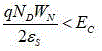

其中,ND、WN分别是N柱区掺杂浓度和宽度, NA、WP分别是N柱区掺杂浓度和宽度,q为元电荷,
可见,要提高掺杂浓度,就必须减小P柱和N柱的宽度。如:将N柱掺杂浓度提升到5e13cm-3以上,就需要将其宽度降低到2μm以下。对于600V的超结器件,其P/N柱深度通常超过30μm,因此挖槽的深宽比将达到15:1以上。这给挖槽和外延填充造成了很大的工艺难度。It can be seen that in order to increase the doping concentration, the widths of the P and N columns must be reduced. For example, to increase the doping concentration of the N column to more than 5e13cm -3 , it is necessary to reduce its width to less than 2μm. For 600V superjunction devices, the P/N column depth is usually more than 30μm, so the aspect ratio of the trench will reach more than 15:1. This creates great technological difficulties for trenching and epitaxial filling.
本发明在超结MOSFET器件的基础上,在P柱与N柱间引入低掺杂N-区或本征区。从工艺上,刻蚀的深槽宽度大于实际形成的P柱宽度,因而减小了沟槽的深宽比,降低了刻蚀难度和外延填充难度。从器件结构上,本发明器件的PN柱的相互耗尽因为中间层的存在使器件横向电场由三角形分布优化为梯形分布。如图5所示,在临界击穿电场相同的情况下,本发明结构的横向电场的积分面积更大,可提高器件的横向击穿电压。同时根据泊松方程,电场斜率越大,掺杂浓度越高,本发明的N柱区可采用更高的掺杂浓度,有利于降低器件的导通电阻。当作为中间层的低掺杂N-区和N柱区的杂质总量等于P柱的杂质总量时,漂移区能够全耗尽,器件的纵向击穿电压不受影响。表1为现有超结MOSFET与本发明改进的超结MOSFET的基本电学参数比较,可见在同样的阈值电压下,本发明具有更高的击穿电压和更低的导通电阻。Based on the superjunction MOSFET device, the present invention introduces a low-doped N-region or an intrinsic region between the P-column and the N-column. From the technical point of view, the width of the etched deep groove is larger than the width of the actually formed P column, thus reducing the aspect ratio of the trench and reducing the difficulty of etching and epitaxial filling. From the structure of the device, the mutual depletion of the PN pillars of the device of the present invention optimizes the lateral electric field of the device from a triangular distribution to a trapezoidal distribution due to the existence of the intermediate layer. As shown in FIG. 5 , when the critical breakdown electric field is the same, the integral area of the lateral electric field of the structure of the present invention is larger, which can improve the lateral breakdown voltage of the device. At the same time, according to Poisson's equation, the larger the electric field slope, the higher the doping concentration, and the N-column region of the present invention can adopt a higher doping concentration, which is beneficial to reduce the on-resistance of the device. When the total amount of impurities in the low-doped N-region and the N-column region as the intermediate layer is equal to the total amount of impurities in the P-column, the drift region can be fully depleted, and the vertical breakdown voltage of the device is not affected. Table 1 is a comparison of the basic electrical parameters of the existing super-junction MOSFET and the improved super-junction MOSFET of the present invention. It can be seen that under the same threshold voltage, the present invention has higher breakdown voltage and lower on-resistance.
表1Table 1
超结MOSFET在正向导通时,漏极加高电压,PN柱为反偏状态,耗尽区的扩展会挤压一部分电流通道,造成器件导通电阻增加,这就是超结MOSFET中存在的JFET效应的影响。对于元胞pitch小于5μm的超结器件,由于PN柱的宽度极小,该效应的影响更加严重。尤其越靠近PN柱底部区域,PN柱之间的反向电压差越大,耗尽区宽度越大,该区域的电阻将显著增大。本发明提出的新结构,其低掺杂N-区在越靠近P柱底部的区域横向尺寸越小,有利于缩小PN柱底部的耗尽区宽度,改善JFET效应的影响。When the superjunction MOSFET is in forward conduction, a high voltage is applied to the drain, and the PN column is in a reverse biased state. The expansion of the depletion region will squeeze a part of the current channel, causing the on-resistance of the device to increase. This is the JFET that exists in the superjunction MOSFET. effect. For superjunction devices with a cell pitch smaller than 5 μm, the effect of this effect is more serious due to the extremely small width of the PN pillars. In particular, the closer to the bottom region of the PN column, the greater the reverse voltage difference between the PN columns, the greater the width of the depletion region, and the greater the resistance of this region. In the new structure proposed by the present invention, the lateral dimension of the low-doped N-region near the bottom of the P-pillar is smaller, which is beneficial to reduce the width of the depletion region at the bottom of the PN-pillar and improve the influence of the JFET effect.
以上结合附图对本发明的实施例进行了详细阐述,但是本发明并不局限于上述的具体实施方式,上述具体实施方式仅仅是示意性的,而不是限制性的,本领域的普通技术人员在本发明的启示下,不脱离本发明宗旨和权利要求所保护范围的情况下还可以做出很多变形,这些均属于本发明的保护。The embodiments of the present invention have been described in detail above with reference to the accompanying drawings, but the present invention is not limited to the above-mentioned specific embodiments. The above-mentioned specific embodiments are only illustrative rather than restrictive. Under the inspiration of the present invention, many modifications can be made without departing from the spirit of the present invention and the protection scope of the claims, which all belong to the protection of the present invention.
Claims (8)
Priority Applications (1)
| Application Number | Priority Date | Filing Date | Title |
|---|---|---|---|
| CN202210370727.3A CN114464670B (en) | 2022-04-11 | 2022-04-11 | A kind of ultra-low specific conductance superjunction MOSFET and preparation method thereof |
Applications Claiming Priority (1)
| Application Number | Priority Date | Filing Date | Title |
|---|---|---|---|
| CN202210370727.3A CN114464670B (en) | 2022-04-11 | 2022-04-11 | A kind of ultra-low specific conductance superjunction MOSFET and preparation method thereof |
Publications (2)
| Publication Number | Publication Date |
|---|---|
| CN114464670A CN114464670A (en) | 2022-05-10 |
| CN114464670B true CN114464670B (en) | 2022-07-01 |
Family
ID=81417478
Family Applications (1)
| Application Number | Title | Priority Date | Filing Date |
|---|---|---|---|
| CN202210370727.3A Active CN114464670B (en) | 2022-04-11 | 2022-04-11 | A kind of ultra-low specific conductance superjunction MOSFET and preparation method thereof |
Country Status (1)
| Country | Link |
|---|---|
| CN (1) | CN114464670B (en) |
Families Citing this family (2)
| Publication number | Priority date | Publication date | Assignee | Title |
|---|---|---|---|---|
| CN115332340A (en) * | 2022-08-08 | 2022-11-11 | 上海功成半导体科技有限公司 | Super junction VDMOS device with dynamic characteristic adjusted and preparation method thereof |
| CN116864397A (en) * | 2023-09-05 | 2023-10-10 | 深圳市冠禹半导体有限公司 | A method of preparing superjunction MOSFET |
Citations (9)
| Publication number | Priority date | Publication date | Assignee | Title |
|---|---|---|---|---|
| JP2003273355A (en) * | 2002-03-18 | 2003-09-26 | Toshiba Corp | Semiconductor device and method of manufacturing the same |
| JP2006294968A (en) * | 2005-04-13 | 2006-10-26 | Shindengen Electric Mfg Co Ltd | Semiconductor device and manufacturing method thereof |
| JP2009105219A (en) * | 2007-10-23 | 2009-05-14 | Toshiba Corp | Semiconductor device |
| CN103474465A (en) * | 2013-09-06 | 2013-12-25 | 无锡新洁能股份有限公司 | Super-junction MOSFET device and manufacturing method thereof |
| CN203456470U (en) * | 2013-09-06 | 2014-02-26 | 无锡新洁能股份有限公司 | Super junction MOSFET device |
| CN105895689A (en) * | 2015-02-16 | 2016-08-24 | 肖胜安 | Super-junction device structure and manufacturing method thereof |
| CN107994076A (en) * | 2016-10-26 | 2018-05-04 | 深圳尚阳通科技有限公司 | The manufacture method of groove grid super node device |
| CN112786677A (en) * | 2019-11-01 | 2021-05-11 | 南通尚阳通集成电路有限公司 | Super junction device and manufacturing method thereof |
| CN113224164A (en) * | 2021-04-21 | 2021-08-06 | 电子科技大学 | Super junction MOS device |
Family Cites Families (5)
| Publication number | Priority date | Publication date | Assignee | Title |
|---|---|---|---|---|
| JP4182986B2 (en) * | 2006-04-19 | 2008-11-19 | トヨタ自動車株式会社 | Semiconductor device and manufacturing method thereof |
| US7960781B2 (en) * | 2008-09-08 | 2011-06-14 | Semiconductor Components Industries, Llc | Semiconductor device having vertical charge-compensated structure and sub-surface connecting layer and method |
| US9515137B2 (en) * | 2013-02-21 | 2016-12-06 | Infineon Technologies Austria Ag | Super junction semiconductor device with a nominal breakdown voltage in a cell area |
| US20170338302A1 (en) * | 2016-05-23 | 2017-11-23 | Infineon Technologies Ag | Power Semiconductor Device with Charge Balance Design |
| CN111540685A (en) * | 2020-05-29 | 2020-08-14 | 上海华虹宏力半导体制造有限公司 | Method for manufacturing super junction device |
-
2022
- 2022-04-11 CN CN202210370727.3A patent/CN114464670B/en active Active
Patent Citations (9)
| Publication number | Priority date | Publication date | Assignee | Title |
|---|---|---|---|---|
| JP2003273355A (en) * | 2002-03-18 | 2003-09-26 | Toshiba Corp | Semiconductor device and method of manufacturing the same |
| JP2006294968A (en) * | 2005-04-13 | 2006-10-26 | Shindengen Electric Mfg Co Ltd | Semiconductor device and manufacturing method thereof |
| JP2009105219A (en) * | 2007-10-23 | 2009-05-14 | Toshiba Corp | Semiconductor device |
| CN103474465A (en) * | 2013-09-06 | 2013-12-25 | 无锡新洁能股份有限公司 | Super-junction MOSFET device and manufacturing method thereof |
| CN203456470U (en) * | 2013-09-06 | 2014-02-26 | 无锡新洁能股份有限公司 | Super junction MOSFET device |
| CN105895689A (en) * | 2015-02-16 | 2016-08-24 | 肖胜安 | Super-junction device structure and manufacturing method thereof |
| CN107994076A (en) * | 2016-10-26 | 2018-05-04 | 深圳尚阳通科技有限公司 | The manufacture method of groove grid super node device |
| CN112786677A (en) * | 2019-11-01 | 2021-05-11 | 南通尚阳通集成电路有限公司 | Super junction device and manufacturing method thereof |
| CN113224164A (en) * | 2021-04-21 | 2021-08-06 | 电子科技大学 | Super junction MOS device |
Non-Patent Citations (1)
| Title |
|---|
| Capacitive behaviour in Super Junction trench MOSFET devices;A. Villamor,et al;《Proceedings of the 8th Spanish Conference on Electron Devices, CDE"2011》;20110407;全文 * |
Also Published As
| Publication number | Publication date |
|---|---|
| CN114464670A (en) | 2022-05-10 |
Similar Documents
| Publication | Publication Date | Title |
|---|---|---|
| US20150179764A1 (en) | Semiconductor device and method for manufacturing same | |
| US11652166B2 (en) | Power device having super junction and Schottky diode | |
| US20210013310A1 (en) | Silicon Carbide Device with Compensation Layer and Method of Manufacturing | |
| CN106663692A (en) | Semiconductor device and manufacturing method thereof | |
| WO2010044226A1 (en) | Semiconductor device and method for manufacturing same | |
| CN114464670B (en) | A kind of ultra-low specific conductance superjunction MOSFET and preparation method thereof | |
| CN113990757A (en) | MOS device structure and manufacturing method | |
| CN105977302A (en) | Grooved gate MOS having buried layer structure | |
| CN112864246B (en) | Superjunction device and manufacturing method thereof | |
| CN111341830B (en) | Super junction structure and manufacturing method thereof | |
| CN114582863B (en) | Trench gate power device | |
| CN117476772A (en) | Semiconductor groove type field effect transistor device and manufacturing method thereof | |
| CN117613084A (en) | Superjunction device and method of manufacturing the same | |
| JP2006332607A (en) | Semiconductor device | |
| CN111463131A (en) | Superjunction semiconductor device and method of making the same | |
| CN111341828B (en) | Super junction structure and manufacturing method thereof | |
| US12136648B2 (en) | Super junction device and method for making the same | |
| CN106057906A (en) | Accumulated DMOS with P type buried layer | |
| US12002849B2 (en) | Super junction semiconductor device and method of manufacturing the same | |
| CN100502041C (en) | Semiconductor device | |
| CN120882059B (en) | 950V super-junction MOS terminal structure of deep groove filling structure and manufacturing method thereof | |
| CN119342868B (en) | Semiconductor structure and method for forming the same | |
| CN120640744B (en) | Self-aligned double-gate MOSFET and manufacturing process thereof | |
| CN116632068B (en) | Field effect transistor device and manufacturing method thereof | |
| CN118299420B (en) | A coupled voltage-dividing longitudinal field plate device and manufacturing method |
Legal Events
| Date | Code | Title | Description |
|---|---|---|---|
| PB01 | Publication | ||
| PB01 | Publication | ||
| SE01 | Entry into force of request for substantive examination | ||
| SE01 | Entry into force of request for substantive examination | ||
| GR01 | Patent grant | ||
| GR01 | Patent grant |