CN1143169C - Liquid crystal display element with controlled storage capacitance - Google Patents
Liquid crystal display element with controlled storage capacitance Download PDFInfo
- Publication number
- CN1143169C CN1143169C CNB011112034A CN01111203A CN1143169C CN 1143169 C CN1143169 C CN 1143169C CN B011112034 A CNB011112034 A CN B011112034A CN 01111203 A CN01111203 A CN 01111203A CN 1143169 C CN1143169 C CN 1143169C
- Authority
- CN
- China
- Prior art keywords
- liquid crystal
- crystal display
- lines
- display cells
- pixel electrode
- Prior art date
- Legal status (The legal status is an assumption and is not a legal conclusion. Google has not performed a legal analysis and makes no representation as to the accuracy of the status listed.)
- Expired - Fee Related
Links
- 239000004973 liquid crystal related substance Substances 0.000 title claims abstract description 124
- 238000003860 storage Methods 0.000 title claims abstract description 99
- 239000000758 substrate Substances 0.000 claims abstract description 70
- 239000010409 thin film Substances 0.000 claims abstract description 20
- 125000006850 spacer group Chemical group 0.000 claims description 17
- 239000000463 material Substances 0.000 claims description 11
- 238000004519 manufacturing process Methods 0.000 claims description 4
- 239000004020 conductor Substances 0.000 claims description 2
- 238000009413 insulation Methods 0.000 claims 6
- 239000003990 capacitor Substances 0.000 abstract description 13
- 102100036464 Activated RNA polymerase II transcriptional coactivator p15 Human genes 0.000 description 13
- 101000713904 Homo sapiens Activated RNA polymerase II transcriptional coactivator p15 Proteins 0.000 description 13
- 229910004444 SUB1 Inorganic materials 0.000 description 13
- 229910004438 SUB2 Inorganic materials 0.000 description 13
- 101100311330 Schizosaccharomyces pombe (strain 972 / ATCC 24843) uap56 gene Proteins 0.000 description 13
- 101150018444 sub2 gene Proteins 0.000 description 13
- 239000011159 matrix material Substances 0.000 description 11
- 239000003292 glue Substances 0.000 description 10
- 230000005684 electric field Effects 0.000 description 7
- 238000007789 sealing Methods 0.000 description 7
- 239000010408 film Substances 0.000 description 6
- 238000010586 diagram Methods 0.000 description 5
- 238000010521 absorption reaction Methods 0.000 description 4
- 239000004065 semiconductor Substances 0.000 description 4
- 230000007547 defect Effects 0.000 description 3
- 238000000034 method Methods 0.000 description 3
- QAOWNCQODCNURD-UHFFFAOYSA-N Sulfuric acid Chemical compound OS(O)(=O)=O QAOWNCQODCNURD-UHFFFAOYSA-N 0.000 description 2
- 229920001940 conductive polymer Polymers 0.000 description 2
- 239000011521 glass Substances 0.000 description 2
- 229920005989 resin Polymers 0.000 description 2
- 239000011347 resin Substances 0.000 description 2
- 238000002834 transmittance Methods 0.000 description 2
- GSSXLFACIJSBOM-UHFFFAOYSA-N 2h-pyran-2-ol Chemical compound OC1OC=CC=C1 GSSXLFACIJSBOM-UHFFFAOYSA-N 0.000 description 1
- ZCYVEMRRCGMTRW-UHFFFAOYSA-N 7553-56-2 Chemical compound [I] ZCYVEMRRCGMTRW-UHFFFAOYSA-N 0.000 description 1
- 229920000265 Polyparaphenylene Polymers 0.000 description 1
- 229910052581 Si3N4 Inorganic materials 0.000 description 1
- 239000000853 adhesive Substances 0.000 description 1
- 230000001070 adhesive effect Effects 0.000 description 1
- 230000002411 adverse Effects 0.000 description 1
- HSFWRNGVRCDJHI-UHFFFAOYSA-N alpha-acetylene Natural products C#C HSFWRNGVRCDJHI-UHFFFAOYSA-N 0.000 description 1
- 150000004982 aromatic amines Chemical class 0.000 description 1
- 150000001495 arsenic compounds Chemical class 0.000 description 1
- 230000005540 biological transmission Effects 0.000 description 1
- 239000006229 carbon black Substances 0.000 description 1
- 239000011248 coating agent Substances 0.000 description 1
- 238000000576 coating method Methods 0.000 description 1
- 238000005520 cutting process Methods 0.000 description 1
- 230000001934 delay Effects 0.000 description 1
- 230000002542 deteriorative effect Effects 0.000 description 1
- 238000009826 distribution Methods 0.000 description 1
- 230000000694 effects Effects 0.000 description 1
- 230000005669 field effect Effects 0.000 description 1
- 125000000524 functional group Chemical group 0.000 description 1
- 125000000623 heterocyclic group Chemical group 0.000 description 1
- 239000012535 impurity Substances 0.000 description 1
- AMGQUBHHOARCQH-UHFFFAOYSA-N indium;oxotin Chemical compound [In].[Sn]=O AMGQUBHHOARCQH-UHFFFAOYSA-N 0.000 description 1
- 239000003999 initiator Substances 0.000 description 1
- 229910052740 iodine Inorganic materials 0.000 description 1
- 239000011630 iodine Substances 0.000 description 1
- 229920000554 ionomer Polymers 0.000 description 1
- WABPQHHGFIMREM-UHFFFAOYSA-N lead(0) Chemical compound [Pb] WABPQHHGFIMREM-UHFFFAOYSA-N 0.000 description 1
- 238000012986 modification Methods 0.000 description 1
- 230000004048 modification Effects 0.000 description 1
- 238000002161 passivation Methods 0.000 description 1
- 230000000149 penetrating effect Effects 0.000 description 1
- 238000000206 photolithography Methods 0.000 description 1
- 229920001197 polyacetylene Polymers 0.000 description 1
- 229920000642 polymer Polymers 0.000 description 1
- 238000006116 polymerization reaction Methods 0.000 description 1
- -1 polyphenylene Polymers 0.000 description 1
- 230000005855 radiation Effects 0.000 description 1
- 229910052710 silicon Inorganic materials 0.000 description 1
- 239000010703 silicon Substances 0.000 description 1
- HQVNEWCFYHHQES-UHFFFAOYSA-N silicon nitride Chemical compound N12[Si]34N5[Si]62N3[Si]51N64 HQVNEWCFYHHQES-UHFFFAOYSA-N 0.000 description 1
- 239000013589 supplement Substances 0.000 description 1
- YVTHLONGBIQYBO-UHFFFAOYSA-N zinc indium(3+) oxygen(2-) Chemical compound [O--].[Zn++].[In+3] YVTHLONGBIQYBO-UHFFFAOYSA-N 0.000 description 1
Images


Classifications
-
- G—PHYSICS
- G02—OPTICS
- G02F—OPTICAL DEVICES OR ARRANGEMENTS FOR THE CONTROL OF LIGHT BY MODIFICATION OF THE OPTICAL PROPERTIES OF THE MEDIA OF THE ELEMENTS INVOLVED THEREIN; NON-LINEAR OPTICS; FREQUENCY-CHANGING OF LIGHT; OPTICAL LOGIC ELEMENTS; OPTICAL ANALOGUE/DIGITAL CONVERTERS
- G02F1/00—Devices or arrangements for the control of the intensity, colour, phase, polarisation or direction of light arriving from an independent light source, e.g. switching, gating or modulating; Non-linear optics
- G02F1/01—Devices or arrangements for the control of the intensity, colour, phase, polarisation or direction of light arriving from an independent light source, e.g. switching, gating or modulating; Non-linear optics for the control of the intensity, phase, polarisation or colour
- G02F1/13—Devices or arrangements for the control of the intensity, colour, phase, polarisation or direction of light arriving from an independent light source, e.g. switching, gating or modulating; Non-linear optics for the control of the intensity, phase, polarisation or colour based on liquid crystals, e.g. single liquid crystal display cells
- G02F1/133—Constructional arrangements; Operation of liquid crystal cells; Circuit arrangements
- G02F1/1333—Constructional arrangements; Manufacturing methods
- G02F1/1343—Electrodes
-
- G—PHYSICS
- G02—OPTICS
- G02F—OPTICAL DEVICES OR ARRANGEMENTS FOR THE CONTROL OF LIGHT BY MODIFICATION OF THE OPTICAL PROPERTIES OF THE MEDIA OF THE ELEMENTS INVOLVED THEREIN; NON-LINEAR OPTICS; FREQUENCY-CHANGING OF LIGHT; OPTICAL LOGIC ELEMENTS; OPTICAL ANALOGUE/DIGITAL CONVERTERS
- G02F1/00—Devices or arrangements for the control of the intensity, colour, phase, polarisation or direction of light arriving from an independent light source, e.g. switching, gating or modulating; Non-linear optics
- G02F1/01—Devices or arrangements for the control of the intensity, colour, phase, polarisation or direction of light arriving from an independent light source, e.g. switching, gating or modulating; Non-linear optics for the control of the intensity, phase, polarisation or colour
- G02F1/13—Devices or arrangements for the control of the intensity, colour, phase, polarisation or direction of light arriving from an independent light source, e.g. switching, gating or modulating; Non-linear optics for the control of the intensity, phase, polarisation or colour based on liquid crystals, e.g. single liquid crystal display cells
- G02F1/133—Constructional arrangements; Operation of liquid crystal cells; Circuit arrangements
- G02F1/136—Liquid crystal cells structurally associated with a semi-conducting layer or substrate, e.g. cells forming part of an integrated circuit
- G02F1/1362—Active matrix addressed cells
- G02F1/136213—Storage capacitors associated with the pixel electrode
-
- G—PHYSICS
- G02—OPTICS
- G02F—OPTICAL DEVICES OR ARRANGEMENTS FOR THE CONTROL OF LIGHT BY MODIFICATION OF THE OPTICAL PROPERTIES OF THE MEDIA OF THE ELEMENTS INVOLVED THEREIN; NON-LINEAR OPTICS; FREQUENCY-CHANGING OF LIGHT; OPTICAL LOGIC ELEMENTS; OPTICAL ANALOGUE/DIGITAL CONVERTERS
- G02F1/00—Devices or arrangements for the control of the intensity, colour, phase, polarisation or direction of light arriving from an independent light source, e.g. switching, gating or modulating; Non-linear optics
- G02F1/01—Devices or arrangements for the control of the intensity, colour, phase, polarisation or direction of light arriving from an independent light source, e.g. switching, gating or modulating; Non-linear optics for the control of the intensity, phase, polarisation or colour
- G02F1/13—Devices or arrangements for the control of the intensity, colour, phase, polarisation or direction of light arriving from an independent light source, e.g. switching, gating or modulating; Non-linear optics for the control of the intensity, phase, polarisation or colour based on liquid crystals, e.g. single liquid crystal display cells
- G02F1/133—Constructional arrangements; Operation of liquid crystal cells; Circuit arrangements
- G02F1/1333—Constructional arrangements; Manufacturing methods
- G02F1/1343—Electrodes
- G02F1/134309—Electrodes characterised by their geometrical arrangement
- G02F1/134336—Matrix
-
- G—PHYSICS
- G02—OPTICS
- G02F—OPTICAL DEVICES OR ARRANGEMENTS FOR THE CONTROL OF LIGHT BY MODIFICATION OF THE OPTICAL PROPERTIES OF THE MEDIA OF THE ELEMENTS INVOLVED THEREIN; NON-LINEAR OPTICS; FREQUENCY-CHANGING OF LIGHT; OPTICAL LOGIC ELEMENTS; OPTICAL ANALOGUE/DIGITAL CONVERTERS
- G02F2201/00—Constructional arrangements not provided for in groups G02F1/00 - G02F7/00
- G02F2201/12—Constructional arrangements not provided for in groups G02F1/00 - G02F7/00 electrode
- G02F2201/123—Constructional arrangements not provided for in groups G02F1/00 - G02F7/00 electrode pixel
Landscapes
- Physics & Mathematics (AREA)
- Nonlinear Science (AREA)
- Engineering & Computer Science (AREA)
- Mathematical Physics (AREA)
- Chemical & Material Sciences (AREA)
- Crystallography & Structural Chemistry (AREA)
- General Physics & Mathematics (AREA)
- Optics & Photonics (AREA)
- Power Engineering (AREA)
- Microelectronics & Electronic Packaging (AREA)
- Liquid Crystal (AREA)
- Devices For Indicating Variable Information By Combining Individual Elements (AREA)
Abstract
一种液晶显示元件包括:一对基片;夹在一对基片中的液晶层;设置在一个基片上的栅极线和与该栅极线相交的漏极线;设置在栅极线和漏极线的交点的薄膜晶体管;设置在两相邻栅极线和两相邻漏极线所围区域的像素电极;设置在另一个基片上的公共电极。液晶显示元件还备有存储线,它设置在像素电极下面,在它们之间介入绝缘层以便构成电容。每个像素电极在其面向存储线的部分形成有开口。

A liquid crystal display element comprises: a pair of substrates; a liquid crystal layer sandwiched between the pair of substrates; a gate line arranged on one substrate and a drain line crossing the gate line; The thin film transistor at the intersection of the drain lines; the pixel electrode arranged in the area surrounded by two adjacent gate lines and the two adjacent drain lines; and the common electrode arranged on another substrate. The liquid crystal display element is also provided with storage lines, which are arranged under the pixel electrodes with an insulating layer interposed between them to form a capacitor. Each pixel electrode is formed with an opening at a portion thereof facing the storage line.
Description
技术领域technical field
本发明涉及液晶显示元件,具体来说,涉及薄膜晶体管有源矩阵型液晶显示元件,它配备有在像素区由设置在其中的存储线和像素电极构成的存储电容。The present invention relates to a liquid crystal display element, in particular, to a thin film transistor active matrix type liquid crystal display element equipped with a storage capacitor formed of a storage line and a pixel electrode disposed therein in a pixel region.
背景技术Background technique
液晶显示装置广泛地被用作笔记本电脑和显示器监视器的高清晰度彩色显示装置。Liquid crystal display devices are widely used as high-definition color display devices for notebook computers and display monitors.
在液晶显示元件中,常见的有简单矩阵型和有源矩阵型。简单矩阵液晶显示元件包括:一对相对的基片;设置在所述基片之一的内表面的第一组平行条状电极;设置在另一个基片内表面的第二组平行条状电极,所述组电极与第一组平行条状电极交叉;以及夹在两个基片之间的液晶层。有源矩阵液晶显示元件包括:一对相对的基片;设置在所述基片之一的内表面的用于选择各自像素的多个开关元件;以及夹在两个基片之间的液晶层。Among liquid crystal display elements, simple matrix type and active matrix type are common. The simple matrix liquid crystal display element includes: a pair of opposite substrates; a first group of parallel strip electrodes arranged on the inner surface of one of the substrates; a second group of parallel strip electrodes arranged on the inner surface of the other substrate , the set of electrodes intersects the first set of parallel strip electrodes; and a liquid crystal layer sandwiched between the two substrates. An active matrix liquid crystal display element includes: a pair of opposing substrates; a plurality of switching elements for selecting respective pixels disposed on the inner surface of one of the substrates; and a liquid crystal layer sandwiched between the two substrates .
有源矩阵型液晶显示元件分为所谓垂直电场型、一般称为TN(扭转向列)型和所谓水平电场型、一般称为IPS(平面内开关型)。在以TN型为代表所谓垂直电场型中,用于像素选择的两组条状电极被分别设置在一对上、下基片的内表面。在所谓水平电场型中,用于像素选择的两组条状电极只设置在一对上、下基片中的一个基片的内表面。Active matrix liquid crystal display elements are classified into so-called vertical electric field type, generally called TN (twisted nematic) type, and so-called horizontal electric field type, generally called IPS (in-plane switching type). In the so-called vertical electric field type represented by the TN type, two sets of strip electrodes for pixel selection are respectively arranged on the inner surfaces of a pair of upper and lower substrates. In the so-called horizontal electric field type, two sets of strip electrodes for pixel selection are provided only on the inner surface of one of a pair of upper and lower substrates.
在TN型有源矩阵液晶显示元件中,液晶分子的取向例如在一对相对的基片之间被扭转90度。一对偏振器分别设置在液晶显示元件的前后,使得它们的吸收轴与入口侧的偏振器的吸收轴成直角(正交尼科尔棱镜排列),而所述入口侧的偏振器吸收轴则与入口侧基片的摩擦方向(rubbingdirection)平行或垂直。In a TN type active matrix liquid crystal display element, the orientation of liquid crystal molecules is twisted by 90 degrees, for example, between a pair of opposing substrates. A pair of polarizers are arranged at the front and back of the liquid crystal display element respectively, so that their absorption axes are at right angles to the absorption axes of the polarizers on the entrance side (arranged by crossed Nicols), while the absorption axes of the polarizers on the entrance side are Parallel or perpendicular to the rubbing direction of the inlet side substrate.
在TN型有源矩阵液晶显示元件中,先假定没有电场加在液晶层两端。入射光被入口侧偏振器转换成线性偏振光,所述线性偏振光沿液晶分子的扭转传播,然后如果出口侧偏振器的透射轴方位角与进入出口侧偏振器的线性偏振光的一致,则所有线性偏振光通过出口侧偏振器并产生白色显示。这是通常所说的打开方式。In the TN-type active matrix liquid crystal display element, it is assumed that there is no electric field applied across the liquid crystal layer. The incident light is converted into linearly polarized light by the entrance-side polarizer, which propagates along the twist of the liquid crystal molecules, and then if the azimuth of the transmission axis of the exit-side polarizer coincides with that of the linearly polarized light entering the exit-side polarizer, then All linearly polarized light passes through the exit side polarizer and produces a white display. This is what is commonly referred to as opening.
下面,假定有电场加到液晶层两端。表示液晶层的液晶分子轴向的平均方向的单位矢量的方向(导向器)与基片的表面垂直,进入液晶层的线性偏振光的方位角不改变,这样它就与出口侧偏振器的吸收角度一致,从而液晶显示元件产生黑色显示。有关进一步的细节,参见“液晶的基础和应用”Industrial Research Association,Tokyo,1991。In the following, it is assumed that an electric field is applied across the liquid crystal layer. The direction of the unit vector (director) representing the average direction of the liquid crystal molecule axial direction of the liquid crystal layer is perpendicular to the surface of the substrate, and the azimuth angle of the linearly polarized light entering the liquid crystal layer does not change, so that it is consistent with the absorption of the exit side polarizer The angles are consistent, so that the liquid crystal display element produces a black display. For further details, see "Basics and Applications of Liquid Crystals," Industrial Research Association, Tokyo, 1991.
如上所述,TN型液晶显示元件包括:由象玻璃这样的材料制造的一对相对的透明绝缘基片;夹在相对的玻璃基片之间的液晶层;一组扫描信号线(下文也称为栅极信号线),它们在所述基片之一的液晶层侧表面上、在直角坐标系统中沿x方向延伸,y方向排列;以及一组与栅极信号线绝缘的漏极线(下文也称为视频信号线),它们在y方向上延伸,在x方向上排列。As mentioned above, the TN-type liquid crystal display element includes: a pair of opposite transparent insulating substrates made of materials such as glass; a liquid crystal layer sandwiched between the opposite glass substrates; a group of scanning signal lines (hereinafter also referred to as are gate signal lines), they extend along the x direction in the Cartesian coordinate system on the liquid crystal layer side surface of one of the substrates, and are arranged in the y direction; and a group of drain lines insulated from the gate signal lines ( Hereinafter also referred to as video signal lines), they extend in the y direction and are arranged in the x direction.
像素区由两个相邻栅极线和两个相邻漏极线所围的区域构成,所有的像素区就构成了显示区。例如,在每个像素区形成作为有源元件(开关元件)的薄膜晶体管(TFT)以及透明像素电极。The pixel area is formed by the area surrounded by two adjacent gate lines and two adjacent drain lines, and all the pixel areas constitute the display area. For example, a thin film transistor (TFT) as an active element (switching element) and a transparent pixel electrode are formed in each pixel region.
供给栅极线的扫描信号将薄膜晶体管接通,然后薄膜晶体管将视频信号从漏极线提供给像素电极。The scan signal supplied to the gate line turns on the thin film transistor, and the thin film transistor supplies a video signal from the drain line to the pixel electrode.
由发光液晶的电介质构成的电容不足以使薄膜晶体管所产生的ON(亮)状态维持指定的时间,因此为每个像素提供一个附加电容,以补充电容的不足。附加电容是通过使像素电极的一部分覆盖在栅极线上,并以绝缘层介入它们之间来实现的。The capacitance formed by the dielectric of the light-emitting liquid crystal is insufficient to maintain the ON (bright) state generated by the thin film transistor for a specified time, so an additional capacitance is provided for each pixel to supplement the lack of capacitance. The additional capacitance is realized by covering a part of the pixel electrode on the gate line with an insulating layer interposed between them.
另一方面,提出一种存储方法:在像素区设置存储线,并利用像素电极、存储线及它们之间的绝缘层构成电容(存储电容)。On the other hand, a storage method is proposed: a storage line is provided in the pixel area, and a capacitor (storage capacitor) is formed by using the pixel electrode, the storage line and an insulating layer between them.
存储型液晶显示装置公开在日本公开特许公报No.Hei 11-231341、日本公开特许公报No.2000-221527和日本实用注册No.2536632中。Storage type liquid crystal display devices are disclosed in Japanese Laid-Open Patent Publication No. Hei 11-231341, Japanese Laid-Open Patent Publication No. 2000-221527, and Japanese Utility Registration No. 2536632.
图13显示存储型液晶显示元件的等效电路。在存储型液晶显示元件中,多根栅极线GL和多根漏极线DL彼此交叉地设置在一对相对的基片中一个基片的显示区AR上;薄膜晶体管TFT设置在栅极线GL和漏极线DL的每一个交叉处,多根存储线STL设置在各栅极线GL之间并与栅极线GL平行。参考字符ITO2表示设置在另一个基片内表面上的共同电极。Fig. 13 shows an equivalent circuit of a memory type liquid crystal display element. In the storage type liquid crystal display element, a plurality of gate lines GL and a plurality of drain lines DL are arranged on the display area AR of one of a pair of opposite substrates so as to cross each other; thin film transistors TFT are arranged on the gate lines. At each intersection of the GL and the drain line DL, a plurality of storage lines STL are disposed between and parallel to the gate lines GL. Reference character ITO2 denotes a common electrode provided on the inner surface of the other substrate.
薄膜晶体管TFT的源极(在一个驱动周期中,源极和漏极的角色可以互换)与像素电极ITO1连接,液晶电容Clc的结构为作为电介质的液晶夹在像素电极ITO1和共同电极ITO2之间,而存储电容Cstg则形成在像素电极ITO1和存储线STL之间。The source of the thin-film transistor TFT (in a driving cycle, the role of the source and the drain can be interchanged) is connected to the pixel electrode ITO1, and the structure of the liquid crystal capacitor Clc is that the liquid crystal as a dielectric is sandwiched between the pixel electrode ITO1 and the common electrode ITO2 The storage capacitor Cstg is formed between the pixel electrode ITO1 and the storage line STL.
共同电极ITO2加有由共同电极驱动电路CDR提供的指定电压(最好是固定电压),而存储线STL加有由存储线驱动电路STR提供的指定电压(最好是固定电压)。参考字符GDR表示栅极线驱动电路,DDR表示漏极线驱动电路,CONT表示用于提供显示信号和定时信号的显示控制电路。The common electrode ITO2 is supplied with a specified voltage (preferably a fixed voltage) provided by the common electrode driving circuit CDR, and the storage line STL is supplied with a specified voltage (preferably a fixed voltage) provided by the storage line driving circuit STR. Reference character GDR denotes a gate line driving circuit, DDR denotes a drain line driving circuit, and CONT denotes a display control circuit for supplying display signals and timing signals.
图14是在存储型液晶显示元件的基片SUB1上构成的单元像素及其附近的主要部件的平面图。在图14中,局部形状和尺寸被放大,以便表示清楚。Fig. 14 is a plan view of a unit pixel formed on a substrate SUB1 of a memory type liquid crystal display element and main components in the vicinity thereof. In Fig. 14, partial shapes and dimensions are exaggerated for clarity.
图15是沿图14的线XV-XV所截取的存储型液晶显示元件的示意的剖面图。15 is a schematic cross-sectional view of the memory type liquid crystal display element taken along line XV-XV in FIG. 14 .
在图14中,在由两个相邻栅极线GL和与这两根栅极线GL相交的两个相邻漏极线所围的区域构成每个像素,并且每个像素在交叉区域备有薄膜晶体管TFT。薄膜晶体管TFT包括:栅极线GL;覆盖在栅极线GL上的绝缘薄膜(为避免示图过分复杂而未显示);在所述绝缘薄膜上形成的、与所述绝缘薄膜一起由非晶硅制成的半导体层100;设置在半导体层100上彼此行对应的源电极SD1和漏极电极SD2。在漏极线DL的下面设置与半导体层100构成一个整体的半导体层,以便减小台阶高度。参考字符SH表示光屏蔽构件,参考数字102则是在栅极线GL上构造的一个开口,用于减少线状缺陷(line defects)。In FIG. 14, each pixel is formed in an area surrounded by two adjacent gate lines GL and two adjacent drain lines intersecting the two gate lines GL, and each pixel is prepared in the intersecting area. There are thin film transistors TFT. The thin film transistor TFT includes: a gate line GL; an insulating film covering the gate line GL (not shown to avoid excessive complexity of the drawing); an amorphous film formed on the insulating film together with the insulating film
透明导电薄膜制造的像素电极ITO1形成在像素区中,并且与薄膜晶体管TFT的源电极SD1连接。在像素区形成与栅极线GL平行的、位于像素电极ITO1下边的存储线STL,在所述像素电极ITO1和存储线STL之间介入绝缘层(在图14中为表示清晰而未显示,但是应该理解为存在这个层)。参考数字103表示在绝缘层中形成的接触孔。A pixel electrode ITO1 made of a transparent conductive film is formed in the pixel region and connected to the source electrode SD1 of the thin film transistor TFT. In the pixel area, a storage line STL parallel to the gate line GL and located under the pixel electrode ITO1 is formed, and an insulating layer is interposed between the pixel electrode ITO1 and the storage line STL (not shown for clarity in FIG. 14 , but should be understood as the existence of this layer).
一般使用与栅极线GL的相同的材料并与栅极线GL一起同时制造存储线STL。薄膜晶体管TFT的漏极SD2是作为漏极线DL的延伸部分来构造的。The storage line STL is generally manufactured using the same material as that of the gate line GL and simultaneously with the gate line GL. The drain SD2 of the thin film transistor TFT is configured as an extension of the drain line DL.
如图15所示,在也称为“薄膜晶体管基片”的基片SUB1内表面上按照指定的顺序形成存储线STL,最好由氮化硅制造的第一绝缘层SiN,由钝化层构成的第二绝缘层PAS,以及像素电极ITO1。在另一个基片SUB2的内表面上形成共同电极ITO2。液晶层LC夹在两上基片SUB1和SUB2之间。As shown in Figure 15, on the inner surface of the substrate SUB1, which is also called "thin film transistor substrate", the storage lines STL are formed in the specified order, preferably the first insulating layer SiN made of silicon nitride, and the passivation layer The second insulating layer PAS and the pixel electrode ITO1 are formed. A common electrode ITO2 is formed on the inner surface of the other substrate SUB2. The liquid crystal layer LC is sandwiched between the two upper substrates SUB1 and SUB2.
虽然图14和图15中未显示,但是在像素电极ITO1和共同电极ITO2与液晶层直接接触的相应的表面上设置了用于将液晶分子定向的定向薄膜。在彩色液晶显示元件中,在共同电极ITO2之下和基片SUB2之上设置了三色滤光片;在此情况下,基片SUB2也称为“彩色滤光基片”。Although not shown in FIGS. 14 and 15 , alignment films for aligning liquid crystal molecules are provided on the respective surfaces of the pixel electrode ITO1 and the common electrode ITO2 that are in direct contact with the liquid crystal layer. In a color liquid crystal display element, a three-color filter is arranged under the common electrode ITO2 and on the substrate SUB2; in this case, the substrate SUB2 is also called a "color filter substrate".
在图15中,以影线区表示的存储电容Cstg由像素电极ITO1,存储线STL,第一绝缘层SiN和第二绝缘层PAS构成。In FIG. 15, the storage capacitor Cstg represented by the hatched area is composed of the pixel electrode ITO1, the storage line STL, the first insulating layer SiN and the second insulating layer PAS.
存储电容Cstg由像素电极ITO1和存储线STL之间的重叠的面积决定,因此由存储线的形状和尺寸决定,所以准确确定存储电容Cstg是困难的,同时增加了电阻。The storage capacitance Cstg is determined by the overlapping area between the pixel electrode ITO1 and the storage line STL, and thus determined by the shape and size of the storage line, so it is difficult to accurately determine the storage capacitance Cstg while increasing the resistance.
共同电极ITO2也覆盖在栅极线GL和漏极线DL之上,液晶层介入于它们之间,因此在共同电极ITO2和漏极线DL及栅极GL之间形成大的布线电容,因此布线所导致的延迟会在显示图像中产生亮度分级。The common electrode ITO2 also covers the gate line GL and the drain line DL, and the liquid crystal layer intervenes between them, so a large wiring capacitance is formed between the common electrode ITO2, the drain line DL and the gate GL, so the wiring The resulting delay can produce brightness gradation in the displayed image.
图16是用于说明由栅极线GL形成的布线电容的液晶显示元件的示意的剖面图,图17是用于说明漏极线DL形成的布线电容的液晶显示元件的示意的剖面图。位于栅极线GL上的有第一绝缘层SiN,第二绝缘层PAS,液晶层LC和共同电极ITO2。位于漏极线DL上的有第一绝缘层SiN,第二绝缘层PAS,液晶层LC和共同电极ITO2。在布线GL,DL与共同电极ITO2之间形成布线电容,其构形分别在图16和图17中用虚线表示。16 is a schematic cross-sectional view of a liquid crystal display element for explaining wiring capacitance formed by gate lines GL, and FIG. 17 is a schematic cross-sectional view of a liquid crystal display element for explaining wiring capacitance formed by drain lines DL. On the gate line GL are a first insulating layer SiN, a second insulating layer PAS, a liquid crystal layer LC and a common electrode ITO2. Located on the drain line DL are a first insulating layer SiN, a second insulating layer PAS, a liquid crystal layer LC and a common electrode ITO2. Wiring capacitors are formed between the wirings GL, DL and the common electrode ITO2, the configurations of which are shown by dotted lines in FIGS. 16 and 17, respectively.
液晶显示元件的尺寸越大,存储线STL,栅极线GL和漏极线DL的长度就越长,布线电容也越大,从而产生所谓布线延迟。因此,存在在所显示图像中出现闪烁或亮度分级的问题。The larger the size of the liquid crystal display element, the longer the length of the storage line STL, the gate line GL and the drain line DL, and the greater the wiring capacitance, thereby causing a so-called wiring delay. Therefore, there is a problem that flickering or brightness gradation occurs in displayed images.
对共同电极ITO2的电压供给是通过导电胶实现的,所述导电胶设置在密封件附近,后者沿着基片的显示区的周边将一对基片密封在一起。导电胶夹在基片SUB1上的共同电极电压供给线与另一个基片SUB2上的共同电极ITO2之间。The voltage supply to the common electrode ITO2 is realized by means of a conductive glue disposed adjacent to a seal which seals the pair of substrates together along the periphery of the display area of the substrates. The conductive glue is sandwiched between the common electrode voltage supply line on the substrate SUB1 and the common electrode ITO2 on the other substrate SUB2.
图18是用于说明导电胶位置的实例的液晶显示元件的平面示意图,所述导电胶用于将基片SUB1上的共同电极电压供给线与基片SUB2上的共同电极ITO2电连接。18 is a schematic plan view of a liquid crystal display element for illustrating an example of the position of conductive glue for electrically connecting the common electrode voltage supply line on the substrate SUB1 with the common electrode ITO2 on the substrate SUB2.
在此液晶显示元件中,通过把基片SUB2置于SUB1之上并将密封件SL介入它们之间而沿着基片SUB1和SUB2的显示区AR的周边将基片SUB1和SUB2密封在一起。In this liquid crystal display element, the substrates SUB1 and SUB2 are sealed together along the peripheries of the display regions AR of the substrates SUB1 and SUB2 by placing the substrate SUB2 over the SUB1 with the sealing member SL interposed therebetween.
在基片SUB1上密封件SL的附近形成共同电极电压供给线(未显示)。在密封操作中,涂敷导电胶CPT,以便覆盖位于诸如涂在基片SUB1上的密封件SL角落位置的共同电极电压供给线,然后把基片SUB2置于基片SUB1之上,使得基片SUB2内表面的共同电极ITO2就与导电胶CPT电连接,从而对共同电极ITO2施加指定电压得以实现。A common electrode voltage supply line (not shown) is formed in the vicinity of the sealing member SL on the substrate SUB1. In the sealing operation, the conductive paste CPT is applied so as to cover the common electrode voltage supply line at the corner position such as the sealing member SL coated on the substrate SUB1, and then the substrate SUB2 is placed on the substrate SUB1 so that the substrate The common electrode ITO2 on the inner surface of the SUB2 is electrically connected to the conductive adhesive CPT, so that a specified voltage is applied to the common electrode ITO2.
对存储线STL的电压供给是通过将存储线电压供给线(未显示)连接到显示区一侧或两侧的电源(存储线驱动电路)来完成的,其中所述存储线电压供给线形成于基片SUB1内表面的密封件SL附近。Voltage supply to the storage line STL is accomplished by connecting a storage line voltage supply line (not shown) formed in the The vicinity of the sealing member SL on the inner surface of the substrate SUB1.
但是,存在这样的问题,存储线越长,电阻和布线电容就越大,于是发生电位的波动,从而在显示图像中产生闪烁和亮度分级,使显示质量劣化。However, there is such a problem that the longer the storage line, the larger the resistance and wiring capacitance, so fluctuations in potential occur, thereby causing flicker and gradation of brightness in the displayed image, deteriorating the display quality.
针对这些问题的措施是,可以增加所涂导电胶的数量,导电胶的涂敷操作要花点时间,这样增加了所谓生产节拍的时间。在采用共同电极电压逆变的驱动方法中,减少电压供给点的数目是困难的,因为要向共同电极提供信号。As a countermeasure against these problems, the amount of conductive glue to be applied can be increased, and the coating operation of the conductive glue takes some time, thus increasing the so-called takt time. In the driving method using common electrode voltage inversion, it is difficult to reduce the number of voltage supply points because signals are supplied to the common electrode.
发明内容Contents of the invention
本发明的目的在于提供一种液晶显示元件,它能够通过解决现有技术中的问题来抑制显示图像中的闪烁和亮度分级的发生,便于确定期望的存储电容,减小存储电容和栅极线或漏极线形成的布线电容,还可以提高生产节拍。The object of the present invention is to provide a liquid crystal display element, which can suppress the occurrence of flicker and brightness gradation in the displayed image by solving the problems in the prior art, facilitate the determination of the desired storage capacitance, reduce the storage capacitance and gate line Or the wiring capacitance formed by the drain line can also improve the production tact.
为了实现上述目的,本发明能够通过在像素电极上设置开口而确定存储线的存储电容值;通过在覆盖栅极线和/或漏极线的共同电极部分(或者位于液晶层的相对侧)设置切口(例如,通过除去共同电极的所述部分以便在其中形成开口)来减小栅极线和/或漏极线的布线电容;或者通过在共同电极和存储线之间设置柱状导电垫片来向共同电极或存储线提供电压而不需要导电胶。In order to achieve the above object, the present invention can determine the storage capacitance value of the storage line by setting an opening on the pixel electrode; Cutting (for example, by removing the portion of the common electrode to form an opening therein) to reduce the wiring capacitance of the gate line and/or drain line; or by providing a columnar conductive spacer between the common electrode and the storage line Provides voltage to a common electrode or storage line without the need for conductive glue.
下面说明根据本发明的液晶显示元件的典型配置。A typical configuration of a liquid crystal display element according to the present invention will be described below.
根据本发明的实施例,提供一种液晶显示元件,它包括:一对基片;夹在所述一对基片之间的液晶层;多根栅极线,设置在所述一对基片中的一个上;多根漏极线,设置成与所述一对基片的所述一个上的所述多根栅极线绝缘并相交;多个薄膜晶体管,设置在所述多根栅极线和所述多根漏极线的交点附近;由透明导电材料制造的多个像素电极,所述多个像素电极中的每一个设置在所述多根栅极线中两根相邻栅极线和所述多根漏极线中两根相邻漏极线所包围的区域,并且通过所述多个薄膜晶体管中对应的一个来驱动;共同电极,设置在所述一对基片中另一基片上,面对所述多个像素电极;以及多根存储线,设置在所述多个像素电极的下面,在所述多根存储线与所述多个像素电极之间介入绝缘层,所述多个像素电极中的每一个在其面向所述多根存储线中对应一根的部分上形成有开口。According to an embodiment of the present invention, a liquid crystal display element is provided, which includes: a pair of substrates; a liquid crystal layer sandwiched between the pair of substrates; a plurality of gate lines arranged on the pair of substrates on one of the substrates; a plurality of drain lines arranged to insulate and intersect with the plurality of gate lines on the one of the pair of substrates; a plurality of thin film transistors arranged on the plurality of gate lines Near the intersection of the line and the plurality of drain lines; a plurality of pixel electrodes made of transparent conductive material, each of the plurality of pixel electrodes is arranged on two adjacent gates in the plurality of gate lines line and the area surrounded by two adjacent drain lines in the plurality of drain lines, and is driven by a corresponding one of the plurality of thin film transistors; the common electrode is arranged on the other of the pair of substrates on a substrate, facing the plurality of pixel electrodes; and a plurality of storage lines arranged under the plurality of pixel electrodes, an insulating layer is interposed between the plurality of storage lines and the plurality of pixel electrodes, Each of the plurality of pixel electrodes has an opening formed on a portion thereof facing a corresponding one of the plurality of storage lines.
在上述液晶显示元件中,所述共同电极在其面向所述多根栅极线的部位形成有切口。或者,所述共同电极在其面向所述多根漏极线的部位形成有切口。In the above-mentioned liquid crystal display element, the common electrode has a cutout formed at a portion thereof facing the plurality of gate lines. Alternatively, the common electrode has cutouts formed at its parts facing the plurality of drain lines.
在上述液晶显示元件中,所述多个像素电极中的每一个和在它下面并且其一部分上形成有开口的所述绝缘层的一部分面向所述多根存储线中对应的一根;所述开口穿透所述多个像素电极和所述绝缘层的全部厚度;多个柱状导电垫片,其中每一个设置在所述各开口中相应的一个中,用于将所述多根存储线之一与所述共同电极电连接。In the above-mentioned liquid crystal display element, each of the plurality of pixel electrodes and a part of the insulating layer below it and on a part of which an opening is formed face a corresponding one of the plurality of storage lines; The opening penetrates the plurality of pixel electrodes and the entire thickness of the insulating layer; a plurality of columnar conductive pads, each of which is disposed in a corresponding one of the openings, for connecting the plurality of storage lines One is electrically connected to the common electrode.
在上述液晶显示元件中,优选地,所述液晶显示元件还包括夹在所述多根存储线和所述多个柱状导电垫片中对应的两者之间的导电层,用于覆盖所述多根存储线。In the above liquid crystal display element, preferably, the liquid crystal display element further includes a conductive layer sandwiched between the plurality of storage lines and corresponding ones of the plurality of columnar conductive spacers, for covering the Multiple storage lines.
在上述液晶显示元件中,所述的一对基片沿其周边用密封件密封在一起;所述液晶显示元件还包括设置在所述一对基片中一个基片上的引线,用于向所述共同电极提供电压;所述多个像素电极中的每一个和在它下面并且其一部分上形成有开口的所述绝缘层的一部分面向所述多根存储线中对应的一根;所述开口穿透所述多个像素电极和所述绝缘层的全部厚度;多个柱状导电垫片,其中每一个设置在所述各开口中相应的一个,用于将所述多根存储线之一与所述共同电极电连接;柱状导电垫片,设置在所述密封件的附近,用于将所述共同电极与所述引线电连接。In the above-mentioned liquid crystal display element, the pair of substrates are sealed together with a sealing member along their peripheries; The common electrode supplies a voltage; each of the plurality of pixel electrodes and a part of the insulating layer below it and a part of which an opening is formed face a corresponding one of the plurality of storage lines; the opening penetrating through the plurality of pixel electrodes and the entire thickness of the insulating layer; a plurality of columnar conductive pads, each of which is disposed in a corresponding one of the openings, for connecting one of the plurality of storage lines with the The common electrode is electrically connected; a columnar conductive gasket is arranged near the sealing member, and is used for electrically connecting the common electrode with the lead wire.
其中,所述液晶显示元件还包括夹在所述多根存储线和所述多个柱状导电垫片中对应的两者之间的导电层,用于覆盖所述多根存储线。Wherein, the liquid crystal display element further includes a conductive layer sandwiched between the plurality of storage lines and corresponding ones of the plurality of columnar conductive pads, for covering the plurality of storage lines.
其中,所述导电层是由与所述多个像素电极相同的材料制造的。或者所述导电层是由像氧化铟锡或氧化铟锌这样的具有导电性的氧化物材料制成的。Wherein, the conductive layer is made of the same material as the plurality of pixel electrodes. Or the conductive layer is made of a conductive oxide material such as indium tin oxide or indium zinc oxide.
在根据本发明的上述液晶显示装置的一个具体结构中,多根栅极线和多根漏极线的交点附近不仅指靠近所述交点的区域,而且指这样的任何区域:在那里,多个薄膜晶体管之一可以分别把其栅极电连接到多根栅极线之一以及把其漏极电连接到多根漏极线之一。例如,所述多个薄膜晶体管中的每一个具有场效应型晶体管结构,后者根据由其栅极施加的电场而在其源极和其漏极之间切换电流。虽然在薄膜晶体管中根据源极和漏极之间的电流方向,源极和漏极的定义是相反的,但是,在本说明书中,为方便起见,将把源极和漏极中连接到多根漏极线之一的一个定义为漏极,而把源极和漏极中连接到多个像素电极之一的另一个定义为源极。In a specific structure of the above-mentioned liquid crystal display device according to the present invention, the vicinity of the intersection of multiple gate lines and multiple drain lines refers not only to an area close to the intersection, but also to any area where multiple One of the thin film transistors may have its gate electrically connected to one of the plurality of gate lines and its drain electrically connected to one of the plurality of drain lines, respectively. For example, each of the plurality of thin film transistors has a field effect type transistor structure that switches current between its source and its drain according to an electric field applied by its gate. Although the definitions of source and drain are reversed in thin film transistors according to the direction of current flow between the source and drain, in this specification, for convenience, the source and drain will be connected to multiple One of the root drain lines is defined as a drain, and the other of the source and drain connected to one of the plurality of pixel electrodes is defined as a source.
本发明不局限于上述配置和后面说明的实施例,而可以在不背离本发明的本质和精神的前提下对本发明进行各种变动和修改。The present invention is not limited to the above configuration and the embodiments described later, but various changes and modifications can be made to the present invention without departing from the essence and spirit of the present invention.
附图说明Description of drawings
图1是根据本发明的存储型液晶显示元件的在基片上形成的单元像素及其附近的主要部件的平面图;Fig. 1 is the plan view of the unit pixel formed on the substrate and its nearby main parts according to the storage type liquid crystal display element of the present invention;
图2是沿图1的线II-II所截取的存储型液晶显示元件的示意的剖面图;Fig. 2 is the schematic sectional view of the storage type liquid crystal display element taken along the line II-II of Fig. 1;
图3是根据本发明的液晶显示元件第二实施例的示意的剖面图,用于说明由栅极线构成的布线电容;FIG. 3 is a schematic cross-sectional view of a second embodiment of a liquid crystal display element according to the present invention, for illustrating wiring capacitance formed by gate lines;
图4是液晶显示元件第二实施例的示意的剖面图,用于说明由漏极线构成的布线电容;Fig. 4 is a schematic cross-sectional view of a second embodiment of a liquid crystal display element for explaining wiring capacitance formed by drain lines;
图5是本发明的液晶显示元件第三实施例主要部件的平面图,用于说明其存储线部分的配置;5 is a plan view of the main components of the third embodiment of the liquid crystal display element of the present invention, used to illustrate the configuration of its storage lines;
图6是沿图5的线VI-VI所截取的液晶显示元件的示意的剖面图;Fig. 6 is a schematic sectional view of the liquid crystal display element taken along the line VI-VI of Fig. 5;
图7是本发明的液晶显示元件第四实施例主要部件的平面图,用于说明其存储线部分的配置;7 is a plan view of the main components of the fourth embodiment of the liquid crystal display element of the present invention, used to illustrate the configuration of its storage line;
图8是沿图7的线VIII-VIII所截取的液晶显示元件的示意的剖面图;8 is a schematic cross-sectional view of a liquid crystal display element taken along line VIII-VIII of FIG. 7;
图9是一个方框图,用于说明采用本发明的液晶显示元件的一般有源矩阵型液晶显示装置的驱动系统的示范的配置;9 is a block diagram for illustrating an exemplary configuration of a driving system of a general active matrix type liquid crystal display device employing a liquid crystal display element of the present invention;
图10是一个方框图,说明图9的液晶显示元件中各个驱动器的大概配置和信号流;Fig. 10 is a block diagram illustrating the approximate configuration and signal flow of each driver in the liquid crystal display element of Fig. 9;
图11是定时图,说明从信号源(主体)提供给显示控制装置的显示数据和从显示控制装置输出到漏极驱动器和栅极驱动器的信号;11 is a timing chart illustrating display data supplied from a signal source (main body) to a display control device and signals output from the display control device to a drain driver and a gate driver;
图12是显示监视器的外形图,它作为装有采用本发明液晶显示元件的液晶显示装置的电子设备的示例;Fig. 12 is an outline view of a display monitor as an example of electronic equipment equipped with a liquid crystal display device employing a liquid crystal display element of the present invention;
图13是存储型液晶显示元件的等效电路;Fig. 13 is an equivalent circuit of a storage type liquid crystal display element;
图14是在存储类型液晶显示元件的基片上形成的单元像素及其附近的主要部件的平面图;Fig. 14 is a plan view of a unit pixel formed on a substrate of a memory-type liquid crystal display element and its surrounding main components;
图15是沿图14的线XV-XV所截取的存储型液晶显示元件的示意的剖面图;Fig. 15 is a schematic sectional view of a storage type liquid crystal display element taken along line XV-XV of Fig. 14;
图16是液晶显示元件的示意的剖面图,用于说明由栅极线构成的布线电容;Fig. 16 is a schematic cross-sectional view of a liquid crystal display element for explaining wiring capacitance constituted by gate lines;
图17是液晶显示元件的示意的剖面图,用于说明由漏极线构成的布线电容;以及FIG. 17 is a schematic cross-sectional view of a liquid crystal display element for explaining wiring capacitance constituted by drain lines; and
图18是用于说明导电胶位置的示例的液晶显示元件的平面示意图,导电胶用于基片上的共同电极电压供给线与另一个基片上的共同电极的电连接。18 is a schematic plan view of a liquid crystal display element for illustrating an example of the position of a conductive paste used for electrical connection of a common electrode voltage supply line on a substrate to a common electrode on another substrate.
具体实施方式Detailed ways
在所述附图中,在所有图中相同的标号表示同一个组件。In said drawings, the same reference numerals denote the same components throughout the figures.
现在参照附图,对本发明的实施例进行详细的说明。Embodiments of the present invention will now be described in detail with reference to the accompanying drawings.
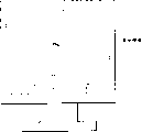
图1是根据本发明的存储型液晶显示元件的在基片上形成的单元像素及其附近的主要部件的平面图,而图2是沿图1的线II-II所截取的存储型液晶显示元件的示意的剖面图。参考字符ALC表示开口,与图14和图15中所用相同的参考字符和标号表示图1和图2中功能上对应的部分。Fig. 1 is the plan view of the unit pixel formed on the substrate and its nearby main parts according to the memory type liquid crystal display element of the present invention, and Fig. 2 is the memory type liquid crystal display element taken along the line II-II of Fig. 1 Schematic sectional view. Reference characters ALC designate openings, and the same reference characters and numerals as used in FIGS. 14 and 15 designate functionally corresponding parts in FIGS. 1 and 2 .
图1和图2中的存储线STL的构成类似于图14和图15中所显示的。至少在覆盖存储线STL的像素电极ITO1上设置开口ALC。如果有需要的话,除像素电极ITO1上的开口ALC外,还可以在覆盖存储线STL的第一绝缘层SiN和第二绝缘层PAS的二者之一或二者上都设置开口ALC。The configuration of the storage line STL in FIGS. 1 and 2 is similar to that shown in FIGS. 14 and 15 . The opening ALC is provided at least on the pixel electrode ITO1 covering the storage line STL. If necessary, in addition to the opening ALC on the pixel electrode ITO1, an opening ALC may also be provided on one or both of the first insulating layer SiN and the second insulating layer PAS covering the storage line STL.
存储线STL上像素电极ITO1中的开口ALC的轮廓的投影最好处在存储线STL的轮廓范围之内,并且,第一和第二绝缘层SiN、PAS中的开口ALC的轮廓最好与像素电极ITO1中的开口ALC的轮廓完全一样或在此轮廓的范围内。The projection of the outline of the opening ALC in the pixel electrode ITO1 on the storage line STL is preferably within the outline range of the storage line STL, and the outlines of the opening ALC in the first and second insulating layers SiN, PAS are preferably consistent with the pixel The profile of the opening ALC in the electrode ITO1 is exactly the same or within the range of this profile.
像在本实施例中那样,在设置存储线STL以便将像素电极ITO1的面积(或在存储线STL的透光性比像素电极ITO1的低情况下的像素电极ITO1的透光区域)分成至少两个部分的情况下,如果在像素电极ITO1上按照上述尺寸关系设置开口ALC,则由于开口ALC的存在使像素电极ITO1上的电荷分布不匀所致的透光性的波动可被忽略。As in this embodiment, when the storage line STL is set so as to divide the area of the pixel electrode ITO1 (or the light-transmitting area of the pixel electrode ITO1 in the case where the light-transmittance of the storage line STL is lower than that of the pixel electrode ITO1) into at least two In the case of two parts, if the opening ALC is provided on the pixel electrode ITO1 according to the above-mentioned size relationship, the fluctuation of the light transmittance caused by the uneven charge distribution on the pixel electrode ITO1 due to the existence of the opening ALC can be ignored.
通过借助至少两种绝缘层(PAS和SiN)将存储线STL和像素电极ITO1彼此隔开,如果其中一个绝缘层发生象针孔这样的缺陷,所造成不良影响(例如,存储线STL和像素电极ITO1之间的短路)会被另一个绝缘层消除掉。因此,像素电极ITO1中的上述开口或像素电极ITO1和第一绝缘层SiN和第二绝缘层PAS两者中的上述开口可以按照期望的尺寸设置而无需考虑绝缘层的可能存在的缺陷。By separating the storage line STL and the pixel electrode ITO1 from each other by means of at least two insulating layers (PAS and SiN), if a defect such as a pinhole occurs in one of the insulating layers, the adverse effects (for example, the storage line STL and the pixel electrode The short circuit between ITO1) will be eliminated by another insulating layer. Therefore, the aforementioned opening in the pixel electrode ITO1 or the aforementioned openings in both the pixel electrode ITO1 and the first insulating layer SiN and the second insulating layer PAS can be set in a desired size without considering possible defects of the insulating layer.
开口ALC穿透像素电极ITO1、第一绝缘层SiN和第二绝缘层PAS的全部厚度,并与存储线STL相对。The opening ALC penetrates through the entire thickness of the pixel electrode ITO1, the first insulating layer SiN, and the second insulating layer PAS, and is opposed to the storage line STL.
按照这样的配置,存储电容Cstg使用图2中第一绝缘层SiN和第二绝缘层PAS的影线部分作为电介质,该存储电容形成于像素电极ITO1沿着其上的开口ALC的部分和与所述部分相对的存储线STL之间。存储电容Cstg的容量值可以通过开口ALC的尺寸来控制。According to such a configuration, the storage capacitor Cstg uses the hatched portion of the first insulating layer SiN and the second insulating layer PAS in FIG. Between the storage lines STL opposite to the above-mentioned part. The capacity value of the storage capacitor Cstg can be controlled by the size of the opening ALC.
在本实施例的液晶显示装置中,对于每一个对图像显示有贡献的像素(换言之,有效显示区域内的像素),最好在像素电极ITO1设置开口ALC,或者同时在像素电极ITO1和绝缘层SiN、PAS上都设置开口ALC。In the liquid crystal display device of the present embodiment, for each pixel that contributes to image display (in other words, the pixel in the effective display area), it is preferable to set the opening ALC on the pixel electrode ITO1, or to provide an opening ALC on the pixel electrode ITO1 and the insulating layer at the same time. Open ALC is set on SiN and PAS.
再者,在本发明中,每个像素的存储电容Cstg的容量值可以通过开口ALC的面积来调整,这样就避免了调整存储线STL尺寸的复杂步骤。从而,无需减小存储线STL在与其延伸方向垂直的方向上的宽度,因此阻止了存储线STL电阻的增加。因此,一个帧期间存储在像素电极ITO1的电荷,在下一个帧期间可以立即被消除掉。Furthermore, in the present invention, the capacity value of the storage capacitor Cstg of each pixel can be adjusted through the area of the opening ALC, thus avoiding the complicated steps of adjusting the size of the storage line STL. Thus, there is no need to reduce the width of the storage line STL in the direction perpendicular to the direction in which it extends, thus preventing an increase in the resistance of the storage line STL. Therefore, the charges stored in the pixel electrode ITO1 during one frame period can be immediately eliminated during the next frame period.
再者,在本实施例中,存储电容Cstg的容量值还可以通过控制每个像素的像素电极ITO1上的开口ALC尺寸来确定,因此可以防止由于存储电容Cstg的变化导致的不均匀的显示和闪烁。Furthermore, in this embodiment, the capacity value of the storage capacitor Cstg can also be determined by controlling the size of the opening ALC on the pixel electrode ITO1 of each pixel, so that uneven display and display caused by changes in the storage capacitor Cstg can be prevented. flashing.
图3是用于说明栅极线GL构成的布线电容的根据本发明的液晶显示元件的第一个实施例的示意的剖面图,图4是用于说明漏极线DL构成的布线电容的液晶显示元件第二个实施例的示意的剖面图。在图3和图4中,参考字符CUT表示在形成于基片SUB2上的共同电极ITO2中设置的切口。与图14和图15中所用的相同的参考字符和标号表示图3和图4中功能上对应的部分。Fig. 3 is a schematic cross-sectional view of a first embodiment of a liquid crystal display element according to the present invention for explaining wiring capacitance constituted by gate line GL, and Fig. 4 is a schematic cross-sectional view for illustrating wiring capacitance constituted by drain line DL. A schematic cross-sectional view of a second embodiment of the element is shown. In FIGS. 3 and 4, reference character CUT denotes a cutout provided in the common electrode ITO2 formed on the substrate SUB2. The same reference characters and numerals as used in FIGS. 14 and 15 denote functionally corresponding parts in FIGS. 3 and 4 .
在本实施例中,形成于栅极线GL和共同电极ITO2之间的布线电容以及形成于漏极线DL和共同电极ITO2之间的布线电容可以被减小到接近零,这样就减小了由布线引起的时间延迟并防止显示中的闪烁和亮度分级的出现。In this embodiment, the wiring capacitance formed between the gate line GL and the common electrode ITO2 and the wiring capacitance formed between the drain line DL and the common electrode ITO2 can be reduced to nearly zero, thus reducing Time delays caused by wiring and prevent flickering and brightness gradation in the display.
图5是本发明的液晶显示元件第三实施例主要部件的平面图,用于说明其存储线STL部分的配置,而图6是沿图5的线VI-VI所截取的液晶显示元件的示意的剖面图。在图5和图6中,参考字符SOC表示柱状导电垫片,SH是光屏蔽构件,与图1-4中所用的相同的参考字符和标号表示图5和图6中功能上对应的部分。5 is a plan view of the main components of the third embodiment of the liquid crystal display element of the present invention, used to illustrate the configuration of its storage line STL portion, and FIG. 6 is a schematic diagram of the liquid crystal display element taken along the line VI-VI of FIG. 5 Sectional view. In FIGS. 5 and 6, reference character SOC denotes a columnar conductive spacer, SH is a light shielding member, and the same reference characters and numerals as used in FIGS. 1-4 denote functionally corresponding parts in FIGS. 5 and 6 .
柱状导电垫片SOC例如是由混入碳黑的感光树脂或导电聚合物制成的。对于前者,一种能够通过光刻方法使之硬化的材料适合于感光树脂。对于后者,例如,导电聚合物可以是属于聚乙炔类,聚苯类等的材料,并混入参杂物,如砷化合物AsF5、硫酸H2SO4和碘I2以及一定痕量的光引发剂;或者杂环聚合物,如poly-pyrol或者离子聚合物,如芳香胺系列。可以对这些材料的官能团进行修改,以便利用光辐射、例如紫外光来引发它们的聚合作用。The columnar conductive spacer SOC is made, for example, of photosensitive resin or conductive polymer mixed with carbon black. For the former, a material that can be hardened by photolithography is suitable for the photosensitive resin. For the latter, for example, the conductive polymer can be a material belonging to the polyacetylene class, polyphenylene class, etc., mixed with impurities such as the arsenic compound AsF 5 , sulfuric acid H 2 SO 4 and iodine I 2 and a certain trace of light Initiator; or heterocyclic polymers, such as poly-pyrol or ionomers, such as aromatic amine series. The functional groups of these materials can be modified to initiate their polymerization with light radiation, such as ultraviolet light.
在本实施例中,在形成于基片SUB1上的存储线STL上的第一和第二绝缘层SiN、PAS以及像素电极ITO1中设置开口ALCN,并且在开口ALCN中设置柱状导电垫片SOC,以便使存储线STL与另一个基片SLUB2上的共同电极ITO2电连接。In this embodiment, an opening ALCN is provided in the first and second insulating layers SiN, PAS and the pixel electrode ITO1 formed on the storage line STL on the substrate SUB1, and a columnar conductive spacer SOC is provided in the opening ALCN, In order to electrically connect the storage line STL to the common electrode ITO2 on another substrate SLUB2.
这种配置无需存储线STL的电压供给线,并在每个像素中设置柱状导电垫片SOC以防止亮度分级和闪烁,因为电压供给点的数量很多,结果在增加存储线STL的布线长度的情况下不会发生由布线引起的时间延迟。This configuration eliminates the need for a voltage supply line for the storage line STL, and provides a columnar conductive spacer SOC in each pixel to prevent brightness gradation and flicker, because the number of voltage supply points is large, resulting in the case of increasing the wiring length of the storage line STL No time delay caused by wiring will occur.
在图5和图6中,这样形成开口ALCN,使得像素电极ITO1中的开口面积比下面的绝缘层PAS和SiN中的开口面积大,其原因是便于柱状导电垫片SOC的加工。如果象图1和图2中情况那样,把像素电极ITO1中的开口面积做成与绝缘层PAS和SiN的完全一样,也不会存在任何问题。In FIG. 5 and FIG. 6, the opening ALCN is formed such that the opening area in the pixel electrode ITO1 is larger than the opening area in the underlying insulating layer PAS and SiN, the reason is to facilitate the processing of the columnar conductive spacer SOC. If, as in the case of FIGS. 1 and 2, the opening area in the pixel electrode ITO1 is made exactly the same as that of the insulating layers PAS and SiN, there will be no problem.
在图5中,在另一个基片SUB2上形成的背面矩阵BM的开口的轮廓以虚线表示,以供参考。In FIG. 5, the outline of the openings of the back matrix BM formed on the other substrate SUB2 is shown in dotted lines for reference.
图7是本发明的液晶显示元件第四实施例的主要部件的平面图,用于说明存储线STL的配置,而图8是沿图7的线VIII-VIII所截取的液晶显示元件的示意的剖面图。在图7和图8中,参考字符ITO3表示导电层,并且与图1-6中所用的相同的参考字符和标号表示图7和图8中功能上对应的部分。7 is a plan view of main parts of a fourth embodiment of a liquid crystal display element of the present invention for explaining the configuration of a storage line STL, and FIG. 8 is a schematic cross-section of the liquid crystal display element taken along line VIII-VIII of FIG. 7 picture. In FIGS. 7 and 8 , reference character ITO3 denotes a conductive layer, and the same reference characters and numerals as used in FIGS. 1-6 denote functionally corresponding parts in FIGS. 7 and 8 .
在本实施例中,在实施例3的开口ALCN底部设置导电层ITO3、以便覆盖存储线STL,并且在导电层ITO3上形成柱状导电垫片SOC。In this embodiment, a conductive layer ITO3 is provided at the bottom of the opening ALCN in Embodiment 3 so as to cover the storage line STL, and a columnar conductive pad SOC is formed on the conductive layer ITO3.
本实施例的配置防止了其他情况下的存储线STL的腐蚀,从而使显示特征保持长时间的稳定,另外还具备实施例3所具有的优点。The configuration of this embodiment prevents the storage line STL from being corroded in other cases, so that the display characteristics remain stable for a long time, and also has the advantages of the third embodiment.
接下来,将说明本发明的实施例5。Next, Embodiment 5 of the present invention will be explained.
在本实施例中,使用第二种柱状导电垫片,来替代设置在图8中密封件SL附近的导电胶CPT。第二种柱状垫片的形状类似于上述设置在像素区的柱状导电垫片(下文称为第一种柱状垫片),但做成具有所需要横截面面积。本实施例实现对共同电极ITO2供给电压而无需使用导电胶,并且通过同时加工第一种柱状垫片和第二种柱状垫片而显著地减少了制造步骤。In this embodiment, the second type of columnar conductive gasket is used to replace the conductive glue CPT disposed near the seal SL in FIG. 8 . The shape of the second type of columnar spacer is similar to that of the aforementioned columnar conductive spacer (hereinafter referred to as the first type of columnar spacer) disposed in the pixel area, but it is made to have a required cross-sectional area. In this embodiment, voltage is supplied to the common electrode ITO2 without using conductive glue, and manufacturing steps are significantly reduced by simultaneously processing the first type of columnar spacer and the second type of columnar spacer.
下面说明使用本发明液晶显示元件的液晶显示装置的一个示例,内容包含其驱动电路的配置和所述液晶显示装置的应用。An example of a liquid crystal display device using the liquid crystal display element of the present invention will be described below, including the configuration of its drive circuit and applications of the liquid crystal display device.
图9是一个方框图,说明采用本发明的液晶显示元件的一般有源矩阵型液晶显示装置的驱动系统的示范的配置。Fig. 9 is a block diagram illustrating an exemplary configuration of a driving system of a general active matrix type liquid crystal display device using the liquid crystal display element of the present invention.
所述液晶显示装置包括:液晶显示元件PNL,它具有夹在一对基片中的液晶层;设置在液晶显示元件PNL周边用于驱动漏极线(也称为数据线、漏极信号线或视频信号线)的电路(IC芯片),即上述漏极驱动器DDR;设置在液晶显示元件PNL周边用于驱动栅极线(也称为栅极信号线或扫描信号线)的电路(IC芯片),即上述栅极驱动器GDR;显示控制装置CRL,它作为显示控制装置,用于将图像显示数据、时钟信号和灰度电压提供给漏极驱动器DDR和栅极驱动器GDR;以及电源电路PWU。显示控制装置CRL接收来自外部信号源(如计算机,个人计算机和电视接收器电路)的显示数据(上述的显示信号)、控制信号时钟、显示定时信号和同步信号。The liquid crystal display device includes: a liquid crystal display element PNL, which has a liquid crystal layer sandwiched between a pair of substrates; arranged around the liquid crystal display element PNL for driving drain lines (also referred to as data lines, drain signal lines or The circuit (IC chip) of the video signal line), that is, the above-mentioned drain driver DDR; the circuit (IC chip) arranged around the liquid crystal display element PNL for driving the gate line (also called gate signal line or scanning signal line) , that is, the above-mentioned gate driver GDR; a display control device CRL as a display control device for supplying image display data, clock signals and grayscale voltages to the drain driver DDR and the gate driver GDR; and the power supply circuit PWU. The display control means CRL receives display data (the above-mentioned display signal), a control signal clock, a display timing signal and a synchronization signal from an external source such as a computer, a personal computer and a television receiver circuit.
显示控制装置CRL包括灰度参考电压产生部件、定时转换器TCON以及其他等等,它将来自外部信号源的显示数据转换成适合在所述液晶显示元件PNL上显示的格式。The display control means CRL includes a gray scale reference voltage generating part, a timing converter TCON, etc., which converts display data from an external signal source into a format suitable for display on said liquid crystal display element PNL.
按图9所示的方式提供用于栅极驱动器GDR和漏极驱动器DDR的显示信号和时钟信号。从漏极驱动器DDR的一级输出的进位信号输出被提供给所述漏极驱动器DDR的下一级的进位输入端。Display signals and clock signals for the gate driver GDR and the drain driver DDR are supplied in the manner shown in FIG. 9 . A carry signal output from one stage of the drain driver DDR is supplied to a carry input terminal of the next stage of the drain driver DDR.
多根存储线STL与栅极线GL平行地被设置在液晶显示元件PNL的显示区域。各存储线STL通过上述实施例所说明的柱状导电垫片与共同电极连接,从电源电路PWU向其提供指定的电压。A plurality of storage lines STL are provided in parallel to the gate lines GL in the display area of the liquid crystal display element PNL. Each storage line STL is connected to the common electrode through the columnar conductive pads described in the above embodiments, and is supplied with a specified voltage from the power supply circuit PWU.
图10是一个方框图,显示图9的液晶显示元件中各个驱动器的大概配置和信号流程。漏极驱动器DDR包括用于显示数据(显示信号)、如视频(图像)信号的数据锁存部分和输出电压产生电路。图中还有灰度参考电压产生部件HTV、复用器MPX、共同电极电压产生部件CVD,共同电极驱动器CDD、电平移动电路LST、门通电压产生部件GOV、门闭电压产生部件GFD、以及安装在安装有图9所示显示控制装置CRL和电源电路PWU的电路板上的DC-DC转换器D/D。FIG. 10 is a block diagram showing an approximate configuration and signal flow of respective drivers in the liquid crystal display element of FIG. 9. Referring to FIG. The drain driver DDR includes a data latch section for display data (display signal), such as a video (image) signal, and an output voltage generation circuit. In the figure, there are gray-scale reference voltage generation part HTV, multiplexer MPX, common electrode voltage generation part CVD, common electrode driver CDD, level shift circuit LST, gate-on voltage generation part GOV, gate-off voltage generation part GFD, and The DC-DC converter D/D is mounted on the circuit board on which the display control device CRL and the power supply circuit PWU shown in FIG. 9 are mounted.
图11是显示从信号源(主体)向控制装置CRL提供的显示数据以及从显示控制装置CRL向漏极驱动器DDR和栅极驱动器GDR输出的信号的定时图。显示控制装置CRL从信号源接收控制信号(时钟信号、显示定时信号和同步信号)并产生作为漏极驱动器DDR控制信号的时钟D1(CL1)、移动时钟D2(CL2)和显示数据,同时产生作为栅极驱动器GDR控制信号的帧启动命令信号FLM、时钟G(CL3)和显示数据。11 is a timing chart showing display data supplied from a signal source (body) to the control device CRL and signals output from the display control device CRL to the drain driver DDR and the gate driver GDR. The display control device CRL receives control signals (clock signal, display timing signal and synchronization signal) from the signal source and generates the clock D1 (CL1) as the control signal of the drain driver DDR, the mobile clock D2 (CL2) and the display data, and generates as the The frame start command signal FLM, clock G (CL3) and display data of the gate driver GDR control signal.
顺便提一下,在系统使用低电位差信号(LVDS信号)来传输来自信号源的显示数据的情况下,在安装有显示控制装置CRL的板(接口板)上安装的LVDS接收电路将来自信号源的LVDS信号转换成原始信号,然后将其提供给栅极驱动器GDR和漏极驱动器DDR。Incidentally, in the case where the system uses a low-potential difference signal (LVDS signal) to transmit display data from the signal source, the LVDS receiving circuit mounted on the board (interface board) on which the display control device CRL is mounted will transmit the display data from the signal source The LVDS signal is converted into a raw signal, which is then provided to the gate driver GDR and the drain driver DDR.
从图11可以看出,用于漏极驱动器DDR的移动时钟信号D2(CL2)的频率与由主计算机等提供的时钟信号(DCLK)和显示数据的频率相同,并且在IBM扩充图形阵列显示标准(XGA)液晶显示元件的情况中所述频率较高,大约40MHz。这种配置的液晶显示装置的特点在于薄的外形和低功耗,因而将来会在各种领域被广泛地用作显示装置。It can be seen from Figure 11 that the frequency of the mobile clock signal D2 (CL2) for the drain driver DDR is the same as the frequency of the clock signal (DCLK) and display data provided by the host computer, etc., and in the IBM Extended Graphics Array Display Standard In the case of (XGA) liquid crystal display elements, the frequency is relatively high, about 40 MHz. A liquid crystal display device of this configuration is characterized by a thin profile and low power consumption, and thus will be widely used as a display device in various fields in the future.
图12是显示器的外形图,它作为采用本发明液晶显示元件的液晶显示装置的电子设备的示例。液晶显示装置用作显示监视器的显示部分。Fig. 12 is an outline view of a display as an example of electronic equipment using the liquid crystal display device of the liquid crystal display element of the present invention. A liquid crystal display device is used as a display portion of a display monitor.
组成显示监视器的液晶显示装置的液晶显示元件PNL具有上述各实施例中所说明的配置的存储线和柱状导电垫片、具有为每个像素适当地建立的存储电容、减少了的布线电容,并且能够提供不发生闪烁并且消除亮度分级使整个显示区的亮度均匀的显示。The liquid crystal display element PNL constituting the liquid crystal display device of the display monitor has storage lines and columnar conductive pads configured as explained in the above embodiments, has storage capacitance properly established for each pixel, reduced wiring capacitance, And it is possible to provide a display in which flicker does not occur and brightness gradation is eliminated so that the brightness of the entire display area is uniform.
不必说,本发明的液晶显示元件的应用不局限于这种显示监视器,本发明的液晶显示元件还可以用作桌上个人计算机的显示器和笔记本个人计算机、电视和其他设备的显示装置。Needless to say, the application of the liquid crystal display element of the present invention is not limited to such display monitors, and the liquid crystal display element of the present invention can also be used as a display of a desktop personal computer and a display device of a notebook personal computer, a television, and others.
如上所述,在本发明中,由存储线构成的存储电容可以通过在像素电极上设置开口来控制,通过在栅极和漏极线上的共同电极中设置切口来减小栅极线和漏极线的布线电容,以及通过在共同电极和存储线之间设置柱状导电垫片来改善加工生产节拍,使得可以不使用任何导电胶或使用最少量的导电胶就可以实现对共同电极和各存储线的电压供给,因此本发明提供了高质量的液晶显示元件。As mentioned above, in the present invention, the storage capacitance constituted by the storage line can be controlled by setting an opening on the pixel electrode, and the gate line and drain line can be reduced by setting a slit in the common electrode on the gate and drain line. The wiring capacitance of the pole line, and the improvement of the processing production cycle by setting a columnar conductive pad between the common electrode and the storage line, so that the common electrode and each storage line can be realized without using any conductive glue or using a minimum amount of conductive glue. Line voltage supply, so the present invention provides high-quality liquid crystal display elements.
Claims (11)
Applications Claiming Priority (2)
| Application Number | Priority Date | Filing Date | Title |
|---|---|---|---|
| JP2000061059 | 2000-03-06 | ||
| JP61059/2000 | 2000-03-06 |
Publications (2)
| Publication Number | Publication Date |
|---|---|
| CN1317711A CN1317711A (en) | 2001-10-17 |
| CN1143169C true CN1143169C (en) | 2004-03-24 |
Family
ID=18581272
Family Applications (1)
| Application Number | Title | Priority Date | Filing Date |
|---|---|---|---|
| CNB011112034A Expired - Fee Related CN1143169C (en) | 2000-03-06 | 2001-03-06 | Liquid crystal display element with controlled storage capacitance |
Country Status (5)
| Country | Link |
|---|---|
| US (1) | US6583829B2 (en) |
| EP (1) | EP1136873B1 (en) |
| KR (1) | KR100356877B1 (en) |
| CN (1) | CN1143169C (en) |
| TW (1) | TW514762B (en) |
Families Citing this family (34)
| Publication number | Priority date | Publication date | Assignee | Title |
|---|---|---|---|---|
| KR100796749B1 (en) | 2001-05-16 | 2008-01-22 | 삼성전자주식회사 | Thin Film Transistor Array Board for Liquid Crystal Display |
| KR100437825B1 (en) * | 2001-07-06 | 2004-06-26 | 엘지.필립스 엘시디 주식회사 | Liquid Crystal Display Device And Method For Fabricating The Same |
| JP2003066488A (en) * | 2001-08-30 | 2003-03-05 | Hitachi Ltd | Liquid crystal display |
| US7242441B2 (en) * | 2002-06-10 | 2007-07-10 | Seiko Epson Corporation | Method for manufacturing electro-optical device, and electro-optical device and electronic device manufactured with this manufacturing method |
| TWI252954B (en) * | 2002-11-11 | 2006-04-11 | Au Optronics Corp | Liquid crystal display device integrating driving circuit on matrix substrate |
| GB0302485D0 (en) * | 2003-02-04 | 2003-03-05 | Plastic Logic Ltd | Pixel capacitors |
| US20040233343A1 (en) * | 2003-05-19 | 2004-11-25 | Samsung Electronics Co., Ltd. | Liquid crystal display and thin film transistor array panel therefor |
| JP2005164854A (en) * | 2003-12-01 | 2005-06-23 | Nec Lcd Technologies Ltd | Liquid crystal display |
| US8006301B2 (en) | 2004-05-19 | 2011-08-23 | Computer Associates Think, Inc. | Method and systems for computer security |
| KR101108391B1 (en) * | 2004-12-31 | 2012-01-30 | 엘지디스플레이 주식회사 | Liquid crystal display |
| JP4083752B2 (en) * | 2005-01-31 | 2008-04-30 | 三菱電機株式会社 | Active matrix substrate and manufacturing method thereof |
| TWM278903U (en) * | 2005-05-23 | 2005-10-21 | Innolux Display Corp | Liquid crystal display device |
| US20060274253A1 (en) * | 2005-06-03 | 2006-12-07 | Wintek Corporation | Conductive spacers for liquid crystal displays |
| CN100454117C (en) * | 2005-06-08 | 2009-01-21 | 友达光电股份有限公司 | Pixel structure suitable for wide-viewing angle liquid crystal display and manufacturing method thereof |
| KR101147090B1 (en) * | 2005-06-29 | 2012-05-17 | 엘지디스플레이 주식회사 | Liquid Crystal Display Device |
| JP4876470B2 (en) * | 2005-07-29 | 2012-02-15 | 三菱電機株式会社 | Display element |
| JP2007093686A (en) * | 2005-09-27 | 2007-04-12 | Mitsubishi Electric Corp | Liquid crystal display device and manufacturing method thereof |
| KR101272336B1 (en) * | 2005-10-20 | 2013-06-07 | 삼성디스플레이 주식회사 | Flat panel display |
| KR101177593B1 (en) * | 2005-12-29 | 2012-08-27 | 엘지디스플레이 주식회사 | Liquid crystal display device |
| KR101300683B1 (en) * | 2006-02-06 | 2013-08-26 | 삼성디스플레이 주식회사 | Liquid crystal display |
| KR101279596B1 (en) * | 2006-09-18 | 2013-06-28 | 삼성디스플레이 주식회사 | Array substrate and display apparatus having the same |
| TW200825520A (en) * | 2006-12-15 | 2008-06-16 | Innolux Display Corp | Liquid crystal panel |
| KR20080082775A (en) * | 2007-03-09 | 2008-09-12 | 삼성전자주식회사 | LCD and its manufacturing method |
| TWI387822B (en) * | 2008-07-01 | 2013-03-01 | Chunghwa Picture Tubes Ltd | Thin film transistor array substrate and manufacturing method thereof |
| JP4600547B2 (en) * | 2008-08-27 | 2010-12-15 | ソニー株式会社 | Liquid crystal display |
| JP4716056B2 (en) * | 2008-12-19 | 2011-07-06 | ソニー株式会社 | Liquid crystal display device and electronic device |
| CN101894835B (en) * | 2009-05-21 | 2012-02-15 | 华映视讯(吴江)有限公司 | Pixel structure and manufacturing method thereof |
| US20110187955A1 (en) * | 2010-02-02 | 2011-08-04 | Chunghwa Picture Tubes, Ltd. | Display device |
| CN102156359B (en) | 2010-06-13 | 2014-05-07 | 京东方科技集团股份有限公司 | Array base plate, liquid crystal panel, liquid crystal display and driving method |
| JP5278777B2 (en) * | 2010-11-09 | 2013-09-04 | Nltテクノロジー株式会社 | Liquid crystal display |
| US9568794B2 (en) * | 2010-12-20 | 2017-02-14 | Semiconductor Energy Laboratory Co., Ltd. | Display device |
| CN105974690B (en) * | 2016-07-22 | 2019-04-26 | 京东方科技集团股份有限公司 | A mask, an array substrate, a display panel and a display device |
| CN109141671B (en) * | 2017-06-27 | 2021-06-01 | 安庆飞凯新材料有限公司 | Flexible over-temperature monitoring device |
| CN110571228B (en) * | 2019-09-26 | 2022-02-01 | 京东方科技集团股份有限公司 | Array substrate, liquid crystal display panel and display device |
Family Cites Families (9)
| Publication number | Priority date | Publication date | Assignee | Title |
|---|---|---|---|---|
| US4639087A (en) * | 1984-08-08 | 1987-01-27 | Energy Conversion Devices, Inc. | Displays having pixels with two portions and capacitors |
| JP2605723B2 (en) * | 1987-07-22 | 1997-04-30 | 日本電気株式会社 | Thin film transistor array type liquid crystal display |
| JPH0563168A (en) * | 1991-08-30 | 1993-03-12 | Sharp Corp | Active matrix substrate |
| KR970011972A (en) * | 1995-08-11 | 1997-03-29 | 쯔지 하루오 | Transmission type liquid crystal display device and manufacturing method thereof |
| CN1148600C (en) * | 1996-11-26 | 2004-05-05 | 三星电子株式会社 | Liquid crystal display using organic insulating material and manufacturing methods thereof |
| JP3226836B2 (en) * | 1997-06-26 | 2001-11-05 | 日本電気株式会社 | Liquid crystal display device and manufacturing method thereof |
| JP3631364B2 (en) | 1998-02-10 | 2005-03-23 | 株式会社アドバンスト・ディスプレイ | Liquid crystal display |
| KR100590742B1 (en) * | 1998-05-11 | 2007-04-25 | 삼성전자주식회사 | Manufacturing method of thin film transistor substrate for liquid crystal display device |
| JP2000221527A (en) | 1999-01-27 | 2000-08-11 | Sharp Corp | Liquid crystal display device |
-
2001
- 2001-03-05 US US09/797,675 patent/US6583829B2/en not_active Expired - Lifetime
- 2001-03-05 TW TW090105036A patent/TW514762B/en not_active IP Right Cessation
- 2001-03-06 EP EP01105303A patent/EP1136873B1/en not_active Expired - Lifetime
- 2001-03-06 CN CNB011112034A patent/CN1143169C/en not_active Expired - Fee Related
- 2001-03-06 KR KR1020010011403A patent/KR100356877B1/en active IP Right Grant
Also Published As
| Publication number | Publication date |
|---|---|
| KR20010087345A (en) | 2001-09-15 |
| EP1136873A3 (en) | 2003-09-03 |
| KR100356877B1 (en) | 2002-10-18 |
| CN1317711A (en) | 2001-10-17 |
| TW514762B (en) | 2002-12-21 |
| US6583829B2 (en) | 2003-06-24 |
| US20010019372A1 (en) | 2001-09-06 |
| EP1136873A2 (en) | 2001-09-26 |
| EP1136873B1 (en) | 2006-06-14 |
Similar Documents
| Publication | Publication Date | Title |
|---|---|---|
| CN1143169C (en) | Liquid crystal display element with controlled storage capacitance | |
| CN1054209C (en) | Liquid crystal display system with active matrix | |
| CN1132384A (en) | Display device and method for driving the same | |
| CN1111754C (en) | Liquid crystal device, electrooptic device, and projection display device using the same | |
| CN1866087A (en) | Single-gap transflective liquid crystal display panel and method for improving its optical characteristics | |
| CN1776508A (en) | Liquid crystal display unit | |
| CN1668969A (en) | LCD Monitor | |
| CN1491371A (en) | Thin film transistor array panel for liquid crystal display | |
| CN1172270A (en) | Liquid crystal display device and method for fabricating thereof | |
| CN108663863B (en) | Array substrate | |
| CN1866350A (en) | Vertical alignment type liquid crystal display device and pixel unit circuit thereof | |
| CN1186761C (en) | Active matrix liquid crystal display unit and its driving and manufacturing method | |
| CN1932594A (en) | Liquid crystal display and driving method thereof | |
| CN1797144A (en) | Liquid crystal display device using in-plane switching mode | |
| WO2020113653A1 (en) | Driving method and driving circuit for display panel | |
| US20160363825A1 (en) | Liquid crystal display | |
| US8144289B2 (en) | Liquid crystal display panel, thin film transistor array substrate and curing line structure for phase separation alignment process | |
| CN2627538Y (en) | Image signal supply circuit and electrooptical panel | |
| CN1677201A (en) | Active matrix substrate and liquid crystal display device with same | |
| CN1804707A (en) | Liquid crystal display device and method of driving the same | |
| CN1290866A (en) | Photoelectric device and its producing method | |
| CN1625713A (en) | Multi-domain liquid crystal display and its thin film transistor substrate | |
| CN1714384A (en) | Liquid crystal display and its driving method | |
| CN1359096A (en) | Electrooptical board and electronic equipment | |
| CN1580924A (en) | Photoelectric panel, photoelectric device and electronic apparatus |
Legal Events
| Date | Code | Title | Description |
|---|---|---|---|
| C10 | Entry into substantive examination | ||
| SE01 | Entry into force of request for substantive examination | ||
| C06 | Publication | ||
| PB01 | Publication | ||
| C14 | Grant of patent or utility model | ||
| GR01 | Patent grant | ||
| ASS | Succession or assignment of patent right |
Owner name: IPS ALPHA SUPPORT CO., LTD. Effective date: 20111125 Owner name: HITACHI DISPLAY CO., LTD. Free format text: FORMER OWNER: HITACHI,LTD. Effective date: 20111125 Owner name: PANASONIC LCD CO., LTD. Free format text: FORMER OWNER: IPS ALPHA SUPPORT CO., LTD. Effective date: 20111125 |
|
| C41 | Transfer of patent application or patent right or utility model | ||
| TR01 | Transfer of patent right |
Effective date of registration: 20111125 Address after: Chiba Prefecture, Japan Co-patentee after: Panasonic Liquid Crystal Display Co.,Ltd. Patentee after: Hitachi Displays, Ltd. Address before: Chiba Prefecture, Japan Co-patentee before: IPS pioneer support society Patentee before: Hitachi Displays, Ltd. Effective date of registration: 20111125 Address after: Chiba Prefecture, Japan Co-patentee after: IPS Pioneer Support Society Patentee after: Hitachi Displays, Ltd. Address before: Chiba Prefecture, Japan Patentee before: Hitachi Displays, Ltd. Effective date of registration: 20111125 Address after: Chiba Prefecture, Japan Patentee after: Hitachi Displays, Ltd. Address before: Tokyo, Japan Patentee before: Hitachi, Ltd. |
|
| C56 | Change in the name or address of the patentee |
Owner name: APAN DISPLAY EAST, INC. Free format text: FORMER NAME: HITACHI DISPLAY CO., LTD. Owner name: JAPAN DISPLAY, INC. Free format text: FORMER NAME: APAN DISPLAY EAST, INC. |
|
| CP01 | Change in the name or title of a patent holder |
Address after: Chiba Prefecture, Japan Patentee after: JAPAN DISPLAY Inc. Patentee after: Panasonic Liquid Crystal Display Co.,Ltd. Address before: Chiba Prefecture, Japan Patentee before: Japan Display East Inc. Patentee before: Panasonic Liquid Crystal Display Co.,Ltd. Address after: Chiba Prefecture, Japan Patentee after: Japan Display East Inc. Patentee after: Panasonic Liquid Crystal Display Co.,Ltd. Address before: Chiba Prefecture, Japan Patentee before: Hitachi Displays, Ltd. Patentee before: Panasonic Liquid Crystal Display Co.,Ltd. |
|
| CP02 | Change in the address of a patent holder |
Address after: Tokyo, Japan Patentee after: JAPAN DISPLAY Inc. Patentee after: Panasonic Liquid Crystal Display Co.,Ltd. Address before: Chiba Prefecture, Japan Patentee before: JAPAN DISPLAY Inc. Patentee before: Panasonic Liquid Crystal Display Co.,Ltd. |
|
| EE01 | Entry into force of recordation of patent licensing contract |
Application publication date: 20011017 Assignee: BOE TECHNOLOGY GROUP Co.,Ltd. Assignor: JAPAN DISPLAY Inc.|Panasonic Liquid Crystal Display Co.,Ltd. Contract record no.: 2013990000688 Denomination of invention: Liquid crystal having controlled storage capacitor Granted publication date: 20040324 License type: Common License Record date: 20131016 |
|
| LICC | Enforcement, change and cancellation of record of contracts on the licence for exploitation of a patent or utility model | ||
| CF01 | Termination of patent right due to non-payment of annual fee | ||
| CF01 | Termination of patent right due to non-payment of annual fee |
Granted publication date: 20040324 Termination date: 20190306 |