CN114281406A - Circuit and method for spatially unique and location independent persistent memory encryption - Google Patents
Circuit and method for spatially unique and location independent persistent memory encryption Download PDFInfo
- Publication number
- CN114281406A CN114281406A CN202110988142.3A CN202110988142A CN114281406A CN 114281406 A CN114281406 A CN 114281406A CN 202110988142 A CN202110988142 A CN 202110988142A CN 114281406 A CN114281406 A CN 114281406A
- Authority
- CN
- China
- Prior art keywords
- address
- persistent
- memory
- range
- generate
- Prior art date
- Legal status (The legal status is an assumption and is not a legal conclusion. Google has not performed a legal analysis and makes no representation as to the accuracy of the status listed.)
- Pending
Links
Images


Classifications
-
- H—ELECTRICITY
- H04—ELECTRIC COMMUNICATION TECHNIQUE
- H04L—TRANSMISSION OF DIGITAL INFORMATION, e.g. TELEGRAPHIC COMMUNICATION
- H04L9/00—Cryptographic mechanisms or cryptographic arrangements for secret or secure communications; Network security protocols
- H04L9/08—Key distribution or management, e.g. generation, sharing or updating, of cryptographic keys or passwords
- H04L9/0861—Generation of secret information including derivation or calculation of cryptographic keys or passwords
- H04L9/0866—Generation of secret information including derivation or calculation of cryptographic keys or passwords involving user or device identifiers, e.g. serial number, physical or biometrical information, DNA, hand-signature or measurable physical characteristics
-
- G—PHYSICS
- G06—COMPUTING OR CALCULATING; COUNTING
- G06F—ELECTRIC DIGITAL DATA PROCESSING
- G06F12/00—Accessing, addressing or allocating within memory systems or architectures
- G06F12/02—Addressing or allocation; Relocation
- G06F12/0223—User address space allocation, e.g. contiguous or non contiguous base addressing
- G06F12/023—Free address space management
- G06F12/0238—Memory management in non-volatile memory, e.g. resistive RAM or ferroelectric memory
-
- G—PHYSICS
- G06—COMPUTING OR CALCULATING; COUNTING
- G06F—ELECTRIC DIGITAL DATA PROCESSING
- G06F12/00—Accessing, addressing or allocating within memory systems or architectures
- G06F12/14—Protection against unauthorised use of memory or access to memory
- G06F12/1408—Protection against unauthorised use of memory or access to memory by using cryptography
-
- G—PHYSICS
- G06—COMPUTING OR CALCULATING; COUNTING
- G06F—ELECTRIC DIGITAL DATA PROCESSING
- G06F12/00—Accessing, addressing or allocating within memory systems or architectures
- G06F12/14—Protection against unauthorised use of memory or access to memory
- G06F12/1416—Protection against unauthorised use of memory or access to memory by checking the object accessibility, e.g. type of access defined by the memory independently of subject rights
- G06F12/1425—Protection against unauthorised use of memory or access to memory by checking the object accessibility, e.g. type of access defined by the memory independently of subject rights the protection being physical, e.g. cell, word, block
- G06F12/1441—Protection against unauthorised use of memory or access to memory by checking the object accessibility, e.g. type of access defined by the memory independently of subject rights the protection being physical, e.g. cell, word, block for a range
-
- G—PHYSICS
- G06—COMPUTING OR CALCULATING; COUNTING
- G06F—ELECTRIC DIGITAL DATA PROCESSING
- G06F9/00—Arrangements for program control, e.g. control units
- G06F9/06—Arrangements for program control, e.g. control units using stored programs, i.e. using an internal store of processing equipment to receive or retain programs
- G06F9/30—Arrangements for executing machine instructions, e.g. instruction decode
- G06F9/30098—Register arrangements
- G06F9/30101—Special purpose registers
-
- G—PHYSICS
- G06—COMPUTING OR CALCULATING; COUNTING
- G06F—ELECTRIC DIGITAL DATA PROCESSING
- G06F9/00—Arrangements for program control, e.g. control units
- G06F9/06—Arrangements for program control, e.g. control units using stored programs, i.e. using an internal store of processing equipment to receive or retain programs
- G06F9/30—Arrangements for executing machine instructions, e.g. instruction decode
- G06F9/30145—Instruction analysis, e.g. decoding, instruction word fields
Landscapes
- Engineering & Computer Science (AREA)
- Theoretical Computer Science (AREA)
- Physics & Mathematics (AREA)
- General Engineering & Computer Science (AREA)
- General Physics & Mathematics (AREA)
- Computer Security & Cryptography (AREA)
- Software Systems (AREA)
- Computer Networks & Wireless Communication (AREA)
- Signal Processing (AREA)
- Storage Device Security (AREA)
Abstract
Systems, methods, and apparatuses for implementing spatially unique and location independent persistent memory encryption are described. In one embodiment, a system on a chip (SoC) includes: at least one persistent range register to indicate a persistent range of the memory; address modification circuitry for checking whether an address of a memory store request is within a persistent range indicated by at least one persistent range register; and when the address is within the persistent range, appending a unique identifier value for the component corresponding to the memory store request for the address to generate a modified address, and outputting the modified address as an output address; and outputting the address as an output address when the address is not within the persistent range; and an encryption engine circuit for generating a ciphertext based on the output address.
Description
Technical Field
The present disclosure relates generally to electronics, and more particularly, embodiments of the present disclosure relate to circuitry for implementing spatially unique and location independent persistent memory encryption.
Background
The processor or set of processors executes instructions from an instruction set, such as an Instruction Set Architecture (ISA). The instruction set is a programming-related part of the computer architecture and generally includes native data types, instructions, register architecture, addressing modes, memory architecture, interrupt and exception handling, and external input and output (I/O). It should be noted that the term instruction may refer herein to a macro-instruction, e.g., an instruction provided to a processor for execution, or to a micro-instruction, e.g., an instruction decoded from a macro-instruction by a decoder of the processor.
Drawings
The present disclosure is illustrated by way of example, and not by way of limitation, in the figures of the accompanying drawings and in which like reference numerals refer to similar elements and in which:
FIG. 1 illustrates a block diagram of a computer system including a plurality of slots with encryption circuitry, according to an embodiment of the present disclosure.
Fig. 2 illustrates a block diagram of an encryption circuit according to an embodiment of the present disclosure.
FIG. 3 is a flow diagram illustrating operations of a method for address modification of multiple persistent memory ranges in accordance with an embodiment of the present disclosure.
FIG. 4 illustrates a persistent control register and an example format thereof according to an embodiment of the present disclosure.
Fig. 5 is a flow diagram illustrating the operation of a method of generating a ciphertext according to an embodiment of the present disclosure.
FIG. 6A is a block diagram illustrating the generic vector friendly instruction format and class A instruction templates thereof according to embodiments of the disclosure.
FIG. 6B is a block diagram illustrating the generic vector friendly instruction format and class B instruction templates thereof according to embodiments of the disclosure.
Fig. 7A is a block diagram illustrating fields for the generic vector friendly instruction format in fig. 6A and 6B, according to an embodiment of the disclosure.
Fig. 7B is a block diagram illustrating fields of the specific vector friendly instruction format of fig. 7A that constitute a full opcode field according to one embodiment of the disclosure.
Fig. 7C is a block diagram illustrating the fields of the specific vector friendly instruction format of fig. 7A that constitute the register memory index field according to one embodiment of the present disclosure.
FIG. 7D is a block diagram illustrating the fields of the specific vector friendly instruction format of FIG. 7A that make up the augmentation operation field 650 according to one embodiment of the present disclosure.
FIG. 8 is a block diagram of a register architecture according to one embodiment of the present disclosure.
FIG. 9A is a block diagram illustrating both an example in-order pipeline and an example register renaming out-of-order issue/execution pipeline, according to embodiments of the disclosure.
FIG. 9B is a block diagram illustrating both an example embodiment of an in-order architecture core and an example register renaming out-of-order issue/execution architecture core to be included in a processor according to an embodiment of the disclosure.
Figure 10A is a block diagram of a single processor core and its connections to an on-die interconnect network and its local subset of a level 2 (L2) cache, according to an embodiment of the present disclosure.
Figure 10B is an expanded view of a portion of the processor core in figure 10A, according to an embodiment of the present disclosure.
FIG. 11 is a block diagram of a processor that may have more than one core, may have an integrated memory controller, and may have an integrated graphics device, according to an embodiment of the disclosure.
Fig. 12 is a block diagram of a system according to one embodiment of the present disclosure.
Fig. 13 is a block diagram of a more specific example system in accordance with an embodiment of the present disclosure.
Fig. 14 illustrates a block diagram of a second more specific example system, according to an embodiment of this disclosure.
Fig. 15 is a block diagram illustrating a system on chip (SoC) according to an embodiment of the present disclosure.
FIG. 16 is a block diagram contrasting the use of a software instruction converter to convert binary instructions in a source instruction set to binary instructions in a target instruction set according to embodiments of the disclosure.
Detailed Description
In the following description, numerous specific details are set forth. However, it is understood that embodiments of the disclosure may be practiced without these specific details. In other instances, well-known circuits, structures and techniques have not been shown in detail in order not to obscure an understanding of this description.
References in the specification to "one embodiment," "an example embodiment," etc., indicate that the embodiment described may include a particular feature, structure, or characteristic, but every embodiment may not necessarily include the particular feature, structure, or characteristic. Moreover, such phrases are not necessarily referring to the same embodiment. Further, when a particular feature, structure, or characteristic is described in connection with an embodiment, it is submitted that it is within the knowledge of one skilled in the art to affect such feature, structure, or characteristic in connection with other embodiments whether or not explicitly described.
A (e.g., hardware) (e.g., having one or more cores) processor may execute instructions (e.g., threads of instructions) to operate on data, for example, to perform arithmetic, logical, or other functions. For example, software may request an operation, and a hardware processor (e.g., one or more cores of the hardware processor) may perform the operation in response to the request. A certainThe operations include accessing one or more memory locations, for example, to store and/or read (e.g., load) data. The system may include a plurality of cores, for example, with a suitable subset of the cores in each of a plurality of slots of a system on a chip (SoC), for example. Each core (e.g., each processor or each socket) may access a data store (e.g., memory). The memory may comprise volatile memory (e.g., dynamic random access memory, DRAM) or persistent (e.g., non-volatile) memory (e.g., non-volatile RAM) (e.g., separate from any system storage, such as, but not limited to, separate from a hard disk drive). One example of persistent memory is a dual in-line memory module (DIMM) (e.g., a non-volatile DIMM) (e.g., OptaneTMmemory), for example, accessible according to the peripheral component interconnect express (PCI-e) standard.
Some systems (e.g., processors) utilize encryption of data to provide security. For example, a processor (e.g., as an Instruction Set Architecture (ISA) extension) may support Total Memory Encryption (TME) (e.g., memory encryption with a single short-time key) and/or multi-key TME (mktme) (e.g., support memory encryption using multiple keys for page granular memory encryption, e.g., with additional support for software supplied keys). Certain embodiments herein utilize multiple types of memory, such as volatile memory (e.g., DRAM) and non-volatile memory (e.g., NVRAM).
In some embodiments, the TME provides the ability to encrypt the entirety of the physical memory of the system. For example, with small changes to the hardware initialization manager code (e.g., basic input/output system (BIOS) firmware), this capability is enabled at a very early stage of the boot process. In certain embodiments, once the TME is configured and locked, the TME will encrypt all data on the SoC's external memory bus using encryption standards/algorithms (e.g., Advanced Encryption Standard (AES), such as, but not limited to, AES using 128-bit keys). In some embodiments, the encryption (e.g., data) key for the TME uses a hardware random number generator implemented in the SoC (e.g., processor), and the key(s) cannot be accessed by software or through the use of an external interface to the SoC. In some embodiments, the TME capability is intended to provide protection for encryption to external memory buses and/or DIMMs.
In some embodiments, a multi-key TME (mktme) establishes and adds support for multiple encryption keys on the TME. In some embodiments, the SoC implementation supports a fixed number of encryption keys, and software may configure the SoC to use a subset of the available keys. In some embodiments, software manages the use of keys, and any section (e.g., page) of memory may be encrypted using each of the available keys. Thus, certain embodiments of the MKTME allow for page granular encryption of memory. In one embodiment (e.g., by default), the MKTME uses the TME encryption key unless explicitly specified by software. Embodiments of the MKTME support software-provided keys in addition to short-time keys generated by a processor (e.g., a Central Processing Unit (CPU)), e.g., not accessible by software or through the use of an external interface to the SoC. In some embodiments, software-provided keys are particularly useful when used with non-volatile memory or when combined with an attestation mechanism and/or used with a key provisioning service. In some embodiments, a tweak (tweek) key for MKTME is provided by software.
In a virtualization scenario, certain embodiments herein allow a Virtual Machine Monitor (VMM) or hypervisor to manage the use of keys to transparently support legacy operating systems without any changes (e.g., so that MKTMEs may also be considered TME virtualization in such a deployment scenario). In some embodiments, an Operating System (OS) is enabled to additionally utilize MKTME capabilities in both native and virtualized environments. In some embodiments, the MKTME is available to each guest OS in the virtualized environment, and the guest OS may utilize the MKTME in the same manner as the native OS.
Certain embodiments herein (e.g., platforms) use TME and/or MKTME to prevent an attacker with physical access to a machine from reading memory (e.g., and stealing any confidential information therein). In some embodiments, the system encrypts the entire memory (e.g., using the TME) at boot time with a single key generated by hardware (e.g., microcode) under the control of hardware initialization manager code (e.g., BIOS firmware). Certain embodiments herein (e.g., platforms) include non-volatile memory (e.g., non-volatile DIMMs) to provide persistent storage that may replace traditional hard drives among other uses such as memory expansion. In certain embodiments, the use of such non-volatile memory (e.g., non-volatile DIMMs) as storage has significant performance benefits over traditional storage. In some embodiments, non-volatile memory (e.g., a non-volatile DIMM) may be accessed through conventional loads and stores using a direct access mode (DAX), similar to volatile system memory (e.g., double data rate synchronous dynamic random access memory (DDR SDRAM)), but different from memory that requires software involvement for DMA from storage (e.g., HDD) to memory for access.
Some embodiments utilize encryption of storage to prevent data loss, for example, on lost/stolen systems. For example, some embodiments utilize encryption of non-volatile memory (e.g., non-volatile DIMMs) (e.g., where some OS platforms provide full volume encryption (e.g., according to the BitLocker standard) for storage encryption). In some embodiments, the multi-key TME provides hardware primitives to encrypt data for both volatile and non-volatile memory. In one embodiment, the AES-XTS standard is used as a cryptographic algorithm to provide the desired security.
To ensure spatial uniqueness across memory space, some encryption (and decryption) processes leverage system physical addresses to fine-tune encryption, e.g., to ensure that the same plaintext gets different ciphertext when encrypted and stored at different physical locations in memory (e.g., to suppress frequency analysis from attackers having physical access to the machine, which may result in leakage of plaintext). While using physical addresses as fine-tuning is effective for volatile memory, it makes some systems vulnerable when used with non-volatile memory, and is prone to data loss when configuration changes occur. One example configuration change is that if a user adds volatile (e.g., DDR) memory to the machine, the memory map changes, and thus also changes the location of the persistent memory. This results in data loss at boot up after memory addition because the physical address used for persistent memory access thereafter is different from the physical address used to store data prior to the addition of volatile memory. Thus, the security requirements of memory encryption to ensure spatial uniqueness directly contradict the persistence requirements.
Certain embodiments herein provide spatially unique, location independent persistent memory encryption that ensures system (e.g., physical) address independent encryption of data on persistent memory while ensuring spatial uniqueness, thereby satisfying both security and persistence requirements. In one embodiment, location-independent encryption presents a novel refinement construct and introduces a unique identifier value (e.g., for each persistent storage device) to be used as part of the encryption to allow multiple persistent storage devices on a single machine. Moreover, device data migration (e.g., moving data from one machine to another) for devices that include persistent storage is achievable, e.g., while still ensuring the security of the data. Embodiments herein allow support of a secure direct access mode that utilizes MKTME's persistent memory. Embodiments herein allow support for a Direct Access (DAX) mode that utilizes MKTMEs while preventing data loss of encrypted data (e.g., ciphertext) stored in non-volatile memory.
Embodiments herein utilize spatially unique, location independent persistent memory encryption, where encryption (e.g., fine-tuning thereof) is generated to meet both security requirements for data protection and functionality requirements for preventing data loss. In some embodiments, location independent memory encryption uses an offset into the persistent memory range for encryption (e.g., trim generation), e.g., using an offset to make the encryption location independent from a memory reconfiguration perspective. In some embodiments, the persistent memory range base address may change without causing data loss when adding and/or removing memory or reconfiguring memory ranges, since the offset into the range remains the same. To ensure that the tweaks are unique across multiple persistent memory devices attached on different memory channels, a unique identifier value is utilized, e.g., a unique ID for each channel is used in the unique identifier value. In some embodiments, a unique identifier value is appended to the input of the encryption (e.g., a trim operation) to ensure that the encryption (e.g., trim) remains unique across multiple persistent memory devices on different memory channels, e.g., appending the unique identifier value to an offset into the persistent memory range and using the resulting value as the trimmed input "address" (e.g., a trim having as one of its inputs the storage address of the encrypted data). In some embodiments, such a fine-tune construct also allows device migration (e.g., shell swap in a client system).
Certain embodiments herein (e.g., using location-independent persistent memory encryption) provide both security and functionality requirements for persistent memory encryption. From a security perspective, certain embodiments herein enable spatial uniqueness in that each location in a device (e.g., a system) gets a unique trim value (e.g., based in part on a unique identifier value) and/or location across multiple devices (e.g., non-volatile memory) on the same platform. From a functional perspective, embodiments herein allow for moving persistent memory ranges (e.g., as a result of any scenario) without corrupting data on the persistent memory device (e.g., without corrupting accessibility of the data). In addition, scenarios in which persistent memory devices are moved from one machine to another may also be supported.
In some embodiments, hardware initialization manager code (e.g., BIOS firmware) is used to program a unique identifier (e.g., used as a unique identifier value) into a host processor (e.g., CPU) register to be used. Some embodiments herein do not change the number of address bits (e.g., a 52-bit address in one embodiment, e.g., by appending a 12-bit wide unique identifier value to a 52-bit address (e.g., offset)).
Turning now to FIG. 1, an example system architecture is depicted. FIG. 1 illustrates a block diagram of a computer system 100, the computer system 100 including a plurality of slots 102, 122 having encryption circuits 114, 134, according to an embodiment of the present disclosure. Although two slots are shown, a single slot or any plurality of slots may be utilized. In FIG. 1, slot _ 0102 includes core _ 0104 and slot _ 1122 includes core _ 0124. The core may be any hardware processor core, e.g., as in the example of core 990 in FIG. 9B. Although multiple cores are shown, each socket may have a single or any number of cores (e.g., where N is any positive integer greater than 1). Each slot may have an identification value, e.g., "slot ID".
Computer system 100 includes persistent control register(s). The persistent control register(s) may be internal to the core or external to the core, for example, within a circuit referred to as an uncore. In one embodiment, the persistent control register(s) (e.g., of a slot) are within the memory controller circuitry (e.g., of the slot). In one embodiment, each of persistent control register(s) 106 of slot 102 includes the same data as the corresponding persistent control register(s) 126 of slot 122. In one embodiment, a single set of persistent control register(s) is utilized for computer system 100. An example persistent control register is discussed below with reference to FIG. 4. Persistent control registers may include one or more persistent range registers, for example, that store value(s) (e.g., provided by execution of hardware initialization manager storage 142) that indicate a range of (e.g., physical) addresses to persist, e.g., in non-volatile memory 120B and/or 140B. Memory access (e.g., store or load) requests may be generated by the cores, e.g., memory access requests may be generated by the execution circuitry 108 of the core 104 (e.g., caused by execution of instructions), and/or memory access requests may be generated by the execution circuitry 128 of the core 124 (e.g., caused by execution of instructions). In some embodiments, the memory access request is serviced by a cache (e.g., cache 112 of socket 102 and/or cache 132 of socket 122). Additionally or alternatively (e.g., for cache misses), the memory access request may be serviced by a memory separate from the cache (e.g., but not a disk drive).
In certain embodiments, computer system 100 includes encryption circuitry (e.g., which utilizes location independent persistent memory encryption as disclosed herein). In one embodiment, a single cryptographic circuit is utilized for both slots 102, 122 of the computer system 100. The encryption circuitry 114 of the socket 102 may receive memory access (e.g., store) requests from one or more of its cores (e.g., from the address generation unit 110 of the execution circuitry 108), and/or the encryption circuitry 134 of the socket 122 may receive memory access (e.g., store) requests from one or more of its cores (e.g., from the address generation unit 130 of the execution circuitry 128). For example, the encryption circuit may perform encryption on the destination address and input of text (e.g., plaintext) to be encrypted (e.g., and a key) to generate ciphertext (e.g., encrypted data). The ciphertext may then be stored in storage, for example, in memory 120 and/or memory 140. The encryption circuitry may perform a decryption operation, for example, for a memory load request.
In certain embodiments, computer system 100 includes a memory controller circuit. In one embodiment, a single memory controller circuit is utilized for multiple slots of computer system 100. The memory controller circuitry 116 of the socket 102 may receive the address of the memory access request, e.g., and also receive payload data (e.g., ciphertext) to be stored at that address for the memory request, and then perform the corresponding access into the memory 120, e.g., via one or more memory buses 118. The memory controller circuitry 136 of the socket 122 may receive the address of the memory access request, e.g., and for the memory request also receive payload data (e.g., ciphertext) to be stored at that address, and then perform the corresponding access into the memory 140, e.g., via one or more memory buses 138. Each Memory Controller (MC) may have an identification value, e.g., "MC ID". The memory and/or memory bus(s) (e.g., memory channels thereof) may have an identification value, e.g., "channel ID". Each memory device (e.g., nonvolatile memory 120B device and nonvolatile memory 140B device) may have its own channel ID. Each slot (e.g., of a single SoC) may have an identification value, e.g., "slot ID. In some embodiments, the memory controller 116 includes a memory controller 116A for volatile memory 120A (e.g., DRAM) and a memory controller 116B for non-volatile memory 120B (e.g., non-volatile DIMM or non-volatile DRAM). In certain embodiments, the memory controller 136 includes a memory controller 136A for volatile memory 140A (e.g., DRAM) and a memory controller 136B for non-volatile memory 140B (e.g., non-volatile DIMM or non-volatile DRAM). Computer system 100 may also include a coupling to secondary (e.g., external) memory (e.g., not directly accessible by the processor), such as a disk (or solid state) drive (e.g., storage unit 1528 in fig. 15).
In one embodiment, hardware initialization manager (non-transitory) storage 142 stores hardware initialization manager firmware (e.g., or software). In one embodiment, hardware initialization manager (non-transitory) storage 142 stores basic input/output system (BIOS) firmware. In another embodiment, the hardware initialization manager (non-transitory) storage 142 stores Unified Extensible Firmware Interface (UEFI) firmware. In certain embodiments (e.g., triggered by power-up or reboot of the processor), computer system 100 (e.g., core 104) executes hardware initialization manager firmware (e.g., or software) stored in hardware initialization manager (non-transitory) storage 142 to initialize system 100 for operation, e.g., to begin executing an Operating System (OS) and/or to initialize and test (e.g., hardware) components of system 100. Fig. 2 illustrates a block diagram of an encryption circuit 200 according to an embodiment of the present disclosure. The encryption circuit 114 and/or the encryption circuit 134 may be examples of the encryption circuit 200. In one embodiment, the encryption circuit 200 operates according to an encryption standard (e.g., AES-XTS), such as when in MKTME mode. In one embodiment, AES-XTS encryption comprises:
t ← AES (Fine key, fine adjustment)
2.PP←P XOR T
3.CC ← AES (data _ Key, PP)
4.C←CC XOR T
Where AES is encrypted according to the AES standard, P is the plaintext to be encrypted, and C is the final ciphertext of the plaintext P.
In some embodiments, the tweaks used in (1.) are generated based on the (e.g., physical) address in which the plaintext is to be stored, e.g., to ensure that the same data at different memory locations is not encrypted to the same ciphertext (hence referred to as a tweaks). In some embodiments, location-dependent encryption (e.g., required from a security perspective) creates functionality issues when used with persistent memory. More specifically, the following may be the case: the base address of the persistent storage in the system changes, and thus the physical address itself (e.g., the physical address was previously used to generate the trim, and thus to produce the ciphertext) changes. One or more ranges of persistent memory may be utilized (e.g., a suitable subset of physical addresses corresponding to non-volatile memory, e.g., as opposed to those corresponding to non-volatile memory). For example, a memory controller (e.g., memory controller circuitry 116 in FIG. 1) directly writes to a first range of memory addresses of a non-volatile memory (e.g., non-volatile memory 120B in FIG. 1), this may be referred to as an Application Direct (AD) range, and/or the memory controller (e.g., memory controller circuitry 116 in fig. 1) first writes to a second (e.g., completely different) range of memory addresses of the volatile memory (e.g., volatile memory 120A in fig. 1) as cache, and then data is written from the volatile memory to the non-volatile memory (e.g., non-volatile memory 120B in fig. 1), which may be referred to as an Application Direct Write Back (ADWB) range (e.g., using volatile (e.g., DDR) memory as cache for persistent data). An example scenario in which a persistent (e.g., AD/ADWB) memory range (e.g., base address) may be moved is listed below:
user override of Cold boot volatile memory (e.g., 1GB DDR5 DIMM capacity)
Add to the system (e.g., add to slot 0102 in fig. 1). All AD-WB and AD addresses will be moved up this amount of memory (e.g., 1GB) in the system address map.
The user adds non-volatile memory (e.g., 1TB non-volatile DIMM) to the system (e.g., to slot 0102 in fig. 1) and configures it all as two levels of memory (2LM), all of which in the system address map will be moved up by that amount of memory (e.g., 1 TB).
The user adds non-volatile memory (e.g., 1TB non-volatile DIMM) to slot 0102 in FIG. 1 and configures it all in AD mode, the AD range for slot 1122 in FIG. 1 will be shifted up by that amount of memory (e.g., 1 TB).
Hardware initialization manager code (e.g., BIOS firmware) detects errors during volatile memory testing and maps out (e.g., logically removes) one or more of the volatile memory devices (e.g., DDR DIMMs).
The hardware initialization manager code (e.g., BIOS firmware) determines that a volatile memory device (e.g., DDR DIMM) that was previously taken offline due to an error can now be enabled.
User-enabled memory backup or mirroring.
The system has an attached Field Programmable Gate Array (FPGA) and is reprogrammed with a new bit stream that affects the size of the FPGA's memory range.
Addition or removal of a low-sized PCIe card except for input/output (MMIO) affecting memory mapping.
In the above, the trimming based on the physical address is changed after the execution of the above scenario. For persistent memory, this results in a (e.g., permanent) data loss because decryption uses an incorrect physical address to generate a trim and returns incorrectly decrypted data (e.g., "garbage"). For volatile memory, the architecture used is both secure and functional in that it is not desirable to retain data for changes in address mapping, e.g., it is not desirable to retain data across boots and/or during boot cycles.
Embodiments herein utilize spatially unique, location independent encryption. In some embodiments of the proposed encryption scheme, the trim for persistent memory encryption is generated using an offset into the persistent memory region rather than using the address itself. Embodiments herein utilize spatially unique, location independent encryption.
The encryption circuit 200 in fig. 2 includes an address modification circuit 206, and the address modification circuit 206 may implement spatially unique and location independent persistent memory encryption. For example, in one embodiment, the encryption circuit 200 receives an input 202 of a destination address (e.g., address "a") (e.g., a destination address of the plaintext 224) (e.g., in response to an encryption request, e.g., a request to encrypt data for storage). In some embodiments, address modification circuitry 206 receives input 202 of address "A" and first compares the address with one or more persistent memory ranges (e.g., as indicated by persistent control register(s) 204) using range checker 208. In some embodiments, when there is a "miss" (e.g., the address is not within one or more ranges of persistent memory), the address modification circuitry 206 outputs the unmodified address "A" 202 as its output, e.g., to the trim circuitry 214. In some embodiments, when there is a "hit" (e.g., an address is within one or more persistent memory ranges), the address modification circuitry 206 outputs a modified value of the address "a'" (e.g., having the same width as the unmodified address "a") as its output, e.g., to the trim circuitry 214. In some embodiments, the unique identifier value 212 is appended (e.g., concatenated) to an appropriate subset of the bits of the address 202. The unique identifier value may be stored in one of persistent control registers 204 (e.g., in register 410 in fig. 4). The unique identifier value 212 may be unique for each persistent memory device (e.g., non-volatile memory 120B in fig. 1 has one unique identifier value and non-volatile memory 120B in fig. 1 has one unique identifier value). The unique identifier value is discussed further below.
In some embodiments, the encryption engine circuit 220 performs one or more encryption operations (e.g., according to an encryption standard) on the input 224 of the plaintext and the input of the tweak value from the tweak circuit 214 (e.g., and the input 222 of the encryption key) to generate the output 226 of the resulting ciphertext. The encryption key 222 may be an encryption key according to an encryption standard (e.g., an AES encryption key).
The encryption circuit 200 may perform a decryption operation, for example, for a memory load request. For example, in one embodiment, the encryption circuit 200 in a decryption mode (e.g., in response to a decryption request, e.g., a request to decrypt data from storage) receives as inputs: the trim value (e.g., from trim buffer 216), encryption key 222, and ciphertext 226, and then plaintext 224 is generated therefrom.
In some embodiments, for persistent memory ranges, address offset generator 210 is used to modify address a for trim generation such that the entire address a is not used as is (e.g., as is the case for non-persistent memory ranges), e.g., such that a modified version of a is calculated and used for trim generation. In some embodiments, the generation of tweaks with spatially unique, location independent encryption is shown in the following pseudo code:
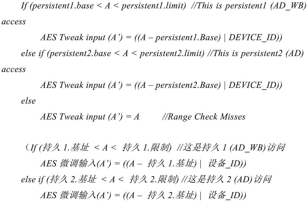
If(persistent1.base<A<persistent1.limit)//This is persistent1(AD_WB) access
AES Tweak input(A’)=((A–persistent1.Base)|APPEND_ID<< MAXPHYS))
else if(persistent2.base<A<persistent2.limit)//This is persistent2(AD) access
AES Tweak input(A’)=((A–persistent2.Base)|APPEND_ID<< MAXPHYS))
else
AES Tweak input(A’)=A//Range Check Misses
(If (persistent 1.base < A < persistent1. Limit)// this is a persistent 1(AD _ WB) access
AES trim input (a') ═ ((a-persistent 1.base) | attached _ ID < < MAXPHYS)
else if (persistent 2. base < A < persistent 2. Limit)// this is a persistent 2(AD) access
AES trim input (a') ═ ((a-persistent 2. base) | attached _ ID < < MAXPHYS)
else
AES fine tune input (a') ═ a// range check miss)
For example, where MAXPHYS is the maximum number of physical address bits in the system, < < < is a left shift, and | is a bitwise logical OR operation. For example, if the input address a is 1016 and the base address (e.g., persistence 1.base) is 1000, the offset is 16. In one embodiment, a range of persistence 1 (e.g., base to limit) represents an ADWB range and a range of persistence 2 (e.g., base to limit) represents an AD range.
In some embodiments, upon receiving an address, a hardware range check is performed to determine whether the incoming transaction is for a (affected) persistent (e.g., AD/ADWB) address range. For example, at boot time, hardware initialization manager code (e.g., BIOS firmware) is used to program range registers (e.g., registers 402, 404, 406, and 408) to cover (e.g., AD/ADWB) multiple ranges that, for example, are to be used by the encryption circuitry to perform range checking on each incoming transaction. In some embodiments, the results of the range check (hit/miss) are passed.
In some embodiments, if the range hits, the address (A) generated for the trim in each slot (e.g., AD/AD-WB) is shifted to 0G, e.g., to the starting page boundary (at 1GB page granularity). For example, if an incoming address matches the persistent range, an offset of the incoming address within the persistent range is determined, e.g., by subtracting the base address of the persistent range from a, and the intermediate result is (a-persistent 1.base), which is passed to, e.g., a trim circuit (e.g., a trim engine circuit).
In some embodiments, if the range hits, the address is normalized across all systems (e.g., across all slots/Memory Controllers (MCs)/channels) and the value of A' is determined, which is passed to, for example, trim circuitry (e.g., trim engine circuitry). In some embodiments, the computed offset may be affected by aliasing (aliasing), which violates security requirements, for example. Thus, in some embodiments, the offset is subject to further (e.g., logical bit) operations to normalize it uniquely across the entire system. Then, in some embodiments, the final value of A' (e.g., used as an input in the trim circuit) is calculated as follows: a ═ a- (a-persistence 1.base) | APPEND _ ID < < MAXPHYS; where APPEND _ ID is a unique (e.g., 12-bit ID) appended to (e.g., AD/ADWB) trim input address. In some embodiments, this ID should be unique across the entire system, e.g., and contain SocketID (slot ID), MC _ ID, and Channel _ ID (Channel _ ID). In one embodiment, hardware initialization manager code (e.g., BIOS firmware) is used to program APPEND _ ID to { SocketID, MC _ ID, Channel _ ID } to avoid aliasing across entire systems, across memory channels; where the operator "," indicates concatenation, and MAXPHYS represents the maximum number of physical address bits in the system (e.g., its processor).
In some embodiments, if the range hits, then modified A (e.g., A') is used as the trim-generated input address instead of unmodified A, and if the range misses, then unmodified A is used as the trim-generated input address. In one embodiment, a range miss implies that the incoming address does not belong to an affected persistent (e.g., AD/ADWB) range, e.g., address modifications (e.g., by address offset generator 210) may be bypassed.
Some embodiments described above provide flexibility for device migration, where a persistent memory device may be moved to another platform, but it may require that the APPEND _ ID (e.g., slot/MC/channel) remain consistent across moves to prevent data loss. Alternatively, the following embodiments eliminate this limitation by assigning a unique identifier value to (e.g., each) persistent memory device (e.g., at manufacture time). In one embodiment, hardware initialization manager code (e.g., BIOS firmware) is used to read the unique identifier from each persistent memory device at boot time and program it into the encryption engine (e.g., into register 410 in FIG. 4). For example, making the unionization across slots/MCs/channels is accomplished by appending a device unique identifier to an offset in the persistent memory range. The fine tuning construction using this alternative embodiment is shown in the following pseudo code example:

in some embodiments, when a new non-volatile memory (e.g., 1TB non-volatile DIMM) device with an AD range is added to a system (e.g., slot), hardware initialization manager code (e.g., BIOS firmware) is used to ensure that it is mapped onto existing AD memory in the system (e.g., in the slot) so that trim values associated with the existing AD memory remain unchanged and no data is lost.
FIG. 3 is a flow diagram illustrating operations 300 of a method for address modification of multiple persistent memory ranges in accordance with an embodiment of the present disclosure. In some embodiments, when a cryptographic circuit (e.g., cryptographic circuit 200) receives a cryptographic request with address a at 302 (e.g., when a TME (total memory encryption) cryptographic circuit receives a CMI (aggregate memory interface) request with address a), the cryptographic circuit is used to determine whether a belongs to a persistent memory range (e.g., AD or AD WB). For example, the encryption circuitry is to check whether the address is within a first (e.g., AD WB) range at 304, and if so, generate and use a modified "address" for trim generation at 306, and if not, check whether the address is within a second (e.g., AD) range at 308, and if so, generate and use the modified "address" for trim generation at 310, and if not, use the system address (e.g., unmodified address) for trim generation at 312. In one embodiment, a modified address is created from the input of address a to the output of address a 'by removing the offset of a and then appending a unique identifier value (e.g., apend _ ID) to make a' unique across the system (e.g., unique across slots, memory controllers, channels, or any one or combination thereof).
In some embodiments, Persistent1 (e.g., AD-WB) and Persistent2 (e.g., AD) ranges apply to transactions with MKTME Virtual Machine (VM) keys, for example, where encryption is bypassed if the transaction comes with a platform key ID (e.g., KeyID 0) and also matches a Persistent1 (e.g., AD _ WB) or Persistent2 (e.g., AD) range.
The various registers that may be added to the system (e.g., to its processor) are illustrated next. In one embodiment, these registers are programmed (e.g., store associated values therein) by a system (including these registers) executing hardware initialization manager code (e.g., BIOS firmware).
FIG. 4 illustrates persistent control register 400 and exemplary format 402 and 410 thereof according to an embodiment of the disclosure. Persistent control registers herein may include one or any combination of persistent control registers 400. In one embodiment, the values stored therein may be stored in a single (e.g., vector) register. In fig. 4, persistent control registers 400 include a register 402 indicating a base address of a first persistent range, a register 404 indicating a limited (e.g., maximum) address of the first persistent range, a register 406 indicating a base address of a second persistent range, a register 408 indicating a limited (e.g., maximum) address of the second persistent range, and a register 410 indicating a persistent address identification value (e.g., unique identifier value (s)). The bit index (e.g., bits [21:0] of the base address field in register 402) and other fields (e.g., including a Reserved (RSVD) field) are examples herein. In some embodiments, the unique identifier value (e.g., APPEND _ ID) is unique for each slot, e.g., such that each slot has its own register 410.
Fig. 5 is a flow diagram illustrating operations 500 of a method of generating a ciphertext according to an embodiment of the present disclosure. Some or all of operations 500 (or other processes, or variations, and/or combinations thereof described herein) are performed under control of the encryption circuitry. The operations 500 include: at block 502, a memory store request for an address in a system is received. The operations 500 further include: at block 504, it is checked by address modification circuitry of the system whether the address is within a persistent range indicated by at least one persistent range register of the system. The operations 500 further include: at block 506, when the address is within the persistent range, appending, by address modification circuitry of the system, a unique identifier value for the component corresponding to the memory store request for the address to generate a modified address, and outputting the modified address as an output address. The operations 500 further include: at block 508, the address is output as an output address by address modification circuitry of the system when the address is not within the durable range. The operations 500 further include: at block 510, ciphertext is generated by a cryptographic engine circuit of the system based on the output address.
Exemplary architectures, systems, etc. that may be used above are detailed below. Exemplary instruction formats that may result in decryption, encryption, reading (e.g., and decryption), and/or writing (e.g., and encryption) are detailed below.
At least some embodiments of the disclosed technology may be described in terms of the following examples:
example 1: an apparatus, comprising:
at least one persistent range register to indicate a persistent range of the memory;
address modification circuitry to check whether an address of a memory store request is within the persistent range indicated by the at least one persistent range register; and
when the address is within the persistent range, appending a unique identifier value for a component corresponding to the memory store request for the address to generate a modified address, and outputting the modified address as an output address; and
outputting the address as the output address when the address is not within the persistent range; and
an encryption engine circuit to generate a ciphertext based on the output address.
Example 2: the apparatus of example 1, wherein the unique identifier value is unique across a multi-socket processor system that includes the apparatus.
Example 3: the apparatus of example 2, wherein the unique identifier value comprises a slot identification value, a memory controller identification value, and a channel identification value.
Example 4: the apparatus of example 1, wherein the memory is a non-volatile random access memory device and the unique identifier value is assigned to the non-volatile random access memory device at the time of manufacture.
Example 5: the apparatus of example 1, wherein the address modification circuitry is to remove a persistent base indicated by a persistent base register from the address to generate an offset into the persistent range, and the unique identifier value is appended to the offset to generate the modified address.
Example 6: the apparatus of example 1, wherein the at least one persistent range register comprises at least one first persistent range register for a first persistent range of memory and at least one second persistent range register for a second persistent range of memory, and the address modification circuitry is to:
when the address is within a first persistent range of the memory, removing a first persistent base address indicated by at least one persistent base register from the address to generate a first offset into the persistent range, and appending the unique identifier value to the first offset to generate the modified address; and
when the address is within a second persistent range of the memory, removing a different second persistent base indicated by the at least one persistent base register from the address to generate a second offset into the persistent range, and appending the unique identifier value to the second offset to generate the modified address.
Example 7: the apparatus of example 6, wherein the first persistent range of memory is a range of non-volatile memory (e.g., non-volatile RAM) that is directly written to by a memory controller, and the second persistent range of memory is a range of non-volatile memory that is indirectly written to by the memory controller via writing to volatile memory (e.g., volatile RAM).
Example 8: the apparatus of example 1, further comprising: a trim circuit to perform a trim operation on the output address from the address modification circuit to generate a trim value, the trim value to be used by the encryption engine circuit to generate the ciphertext.
Example 9: the apparatus of example 8, further comprising: a trim buffer to store a copy of the trim value, wherein the encryption engine circuit is to use the copy of the trim value for a decryption operation on the ciphertext encrypted with the trim value.
Example 10: a method, comprising:
receiving a memory store request for an address in a system;
checking, by address modification circuitry of the system, whether the address is within a persistent range indicated by at least one persistent range register of the system;
when the address is within the persistent range, appending, by the address modification circuitry of the system, a unique identifier value for a component corresponding to the memory store request for the address to generate a modified address, and outputting the modified address as an output address;
outputting, by the address modification circuitry of the system, the address as the output address when the address is not within the persistent range; and
generating, by an encryption engine circuit of the system, a ciphertext based on the output address.
Example 11: the method of example 10, wherein the system is a multi-slot processor system and the unique identifier value is unique across the multi-slot processor system.
Example 12: the method of example 11, wherein the unique identifier value comprises a slot identification value, a memory controller identification value, and a channel identification value.
Example 13: the method of example 10, wherein the memory is a non-volatile random access memory device and the unique identifier value is assigned to the non-volatile random access memory device at the time of manufacture.
Example 14: the method of example 10, further comprising: removing, by the address modification circuitry, a persistent base address indicated by a persistent base register from the address to generate an offset into the persistent range, wherein the appending comprises appending the unique identifier value to the offset to generate the modified address.
Example 15: the method of example 10, further comprising:
removing a first persistent base address indicated by at least one persistent base register from the address to generate a first offset into the persistent range when the address is within a first persistent range of memory indicated by at least one first persistent range register, wherein the appending includes appending the unique identifier value to the first offset to generate the modified address, and
when the address is within a second endurance range of memory indicated by at least one second persistent range register, removing a different second persistent base indicated by the at least one persistent base register from the address to generate a second offset into the persistent range, wherein the appending includes appending the unique identifier value to the second offset to generate the modified address.
Example 16: the method of example 10, further comprising: performing, by a trim circuit of the system, a trim operation on the output address from the address modification circuit to generate a trim value, the trim value used by the encryption engine circuit to generate the ciphertext.
Example 17: the method of example 16, further comprising: storing a copy of the trim value in a trim buffer of the system and using the copy of the trim value for a decryption operation on the ciphertext encrypted with the trim value.
Example 18: a non-transitory machine readable medium storing program code that, when executed by a machine, causes the machine to perform a method comprising:
receiving a memory store request for an address in a system;
checking, by address modification circuitry of the system, whether the address is within a persistent range indicated by at least one persistent range register of the system;
when the address is within the persistent range, appending, by the address modification circuitry of the system, a unique identifier value for a component corresponding to the memory store request for the address to generate a modified address, and outputting the modified address as an output address;
outputting, by the address modification circuitry of the system, the address as the output address when the address is not within the persistent range; and
generating, by an encryption engine circuit of the system, a ciphertext based on the output address.
Example 19: the non-transitory machine readable medium of example 18, wherein the system is a multi-socket processor system and the unique identifier value is unique across the multi-socket processor system.
Example 20: the non-transitory machine readable medium of example 19, wherein the unique identifier value comprises a slot identification value, a memory controller identification value, and a channel identification value.
Example 21: the non-transitory machine readable medium of example 18, wherein the memory is a non-volatile random access memory device and the unique identifier value is assigned to the non-volatile random access memory device at the time of manufacture.
Example 22: the non-transitory machine readable medium of example 18, further comprising: removing, by the address modification circuitry, a persistent base indicated by a persistent base register from the address to generate an offset into the persistent range, wherein the appending comprises appending the unique identifier value to the offset to generate the modified address.
Example 23: the non-transitory machine readable medium of example 18, further comprising:
removing a first persistent base address indicated by at least one persistent base register from the address to generate a first offset into the persistent range when the address is within a first persistent range of memory indicated by at least one first persistent range register, wherein the appending includes appending the unique identifier value to the first offset to generate the modified address, and
when the address is within a second endurance range of memory indicated by at least one second persistent range register, removing a different second persistent base indicated by the at least one persistent base register from the address to generate a second offset into the persistent range, wherein the appending includes appending the unique identifier value to the second offset to generate the modified address.
Example 24: the non-transitory machine readable medium of example 18, further comprising: performing, by a trim circuit of the system, a trim operation on the output address from the address modification circuit to generate a trim value, the trim value used by the encryption engine circuit to generate the ciphertext.
Example 25: the non-transitory machine readable medium of example 24, further comprising: storing a copy of the trim value in a trim buffer of the system and using the copy of the trim value for a decryption operation on the ciphertext encrypted with the trim value.
In yet another embodiment, an apparatus comprises a data storage device that stores code that, when executed by a hardware processor, causes the hardware processor to perform any of the methods disclosed herein. The apparatus may be as described in the detailed description. The method may be as described in the detailed description.
The instruction set may include one or more instruction formats. A given instruction format may define various fields (e.g., number of bits, location of bits) to specify an operation (e.g., opcode) to be performed, as well as operand(s) and/or other data field(s) (e.g., mask) on which the operation is to be performed, and so forth. Some instruction formats are further decomposed by the definition of instruction templates (or subformats). For example, an instruction template for a given instruction format may be defined to have different subsets of the fields of the instruction format (the included fields are typically in the same order, but at least some fields have different bit positions, since fewer fields are included) and/or to have a given field interpreted differently. Thus, each instruction of the ISA is expressed using a given instruction format (and, if defined, a given one of the instruction templates in that instruction format) and includes fields for specifying operations and operands. For example, an exemplary ADD instruction has a particular opcode and instruction format that includes an opcode field to specify the opcode and an operand field to select operands (source 1/destination and source 2); and the ADD meansThe occurrence in the instruction stream will cause the particular contents of the operand fields to be selected for a particular operand. The SIMD extension sets referred to as advanced vector extensions (AVX) (AVX1 and AVX2) and using the Vector Extension (VEX) coding scheme have been introduced and/or released (see, e.g., month 11 of 2018) 64 and IA-32 architecture software developer manuals; and see month 10 2018
 Architectural instruction set extension programming reference).
Exemplary instruction Format
Embodiments of the instruction(s) described herein may be embodied in different formats. Additionally, exemplary systems, architectures, and pipelines are detailed below. Embodiments of the instruction(s) may be executed on such systems, architectures, and pipelines, but are not limited to those detailed.
Universal vector friendly instruction format
The vector friendly instruction format is an instruction format that is appropriate for vector instructions (e.g., there are specific fields dedicated to vector operations). Although embodiments are described in which both vector and scalar operations are supported by the vector friendly instruction format, alternative embodiments use only vector operations by the vector friendly instruction format.
6A-6B are block diagrams illustrating a generic vector friendly instruction format and its instruction templates according to embodiments of the disclosure. FIG. 6A is a block diagram illustrating a generic vector friendly instruction format and class A instruction templates thereof according to embodiments of the disclosure; and FIG. 6B is a block diagram illustrating a generic vector friendly instruction format and class B instruction templates thereof according to embodiments of the disclosure. In particular, class a and class B instruction templates are defined for the generic vector friendly instruction format 600, both of which include instruction templates with no memory access 605 and instruction templates with memory access 620. The term "generic" in the context of a vector friendly instruction format refers to an instruction format that is not tied to any particular instruction set.
Although embodiments of the present disclosure will be described in which the vector friendly instruction format supports the following: a 64 byte vector operand length (or size) and a 32 bit (4 byte) or 64 bit (8 byte) data element width (or size) (and thus, a 64 byte vector consists of 16 elements of a doubleword size, or alternatively 8 elements of a quadword size); a 64 byte vector operand length (or size) and a 16 bit (2 byte) or 8 bit (1 byte) data element width (or size); a 32 byte vector operand length (or size) and a 32 bit (4 byte), 64 bit (8 byte), 16 bit (2 byte) or 8 bit (1 byte) data element width (or size); and a 16 byte vector operand length (or size) and 32 bit (4 byte), 64 bit (8 byte), 16 bit (2 byte), or 8 bit (1 byte) data element width (or size); alternative embodiments may support larger, smaller, and/or different vector operand sizes (e.g., 256 byte vector operands) and larger, smaller, or different data element widths (e.g., 128 bit (16 byte) data element widths).
The class a instruction templates in fig. 6A include: 1) within the instruction templates of no memory access 605, an instruction template of a full round-control type operation 610 of no memory access and an instruction template of a data transform type operation 615 of no memory access are shown; and 2) within the instruction templates of memory access 620, an instruction template of timeliness 625 of memory accesses and an instruction template of non-timeliness 630 of memory accesses are shown. The class B instruction templates in FIG. 6B include: 1) within the instruction templates of no memory access 605, an instruction template of a write mask controlled partial round control type operation 612 of no memory access and an instruction template of a write mask controlled vsize type operation 617 of no memory access are shown; and 2) within the instruction templates of memory access 620, the instruction templates of write mask control 627 of the memory access are shown.
The generic vector friendly instruction format 600 includes the following fields listed below in the order illustrated in fig. 6A-6B.
A modifier field 646-the contents of which distinguish instructions in the generic vector instruction format that specify memory accesses from instructions in the generic vector instruction format that do not specify memory accesses; i.e. to distinguish between instruction templates with no memory access 605 and instruction templates with memory access 620. Memory access operations read and/or write to the memory hierarchy (in some cases specifying source and/or destination addresses using values in registers), while non-memory access operations do not (e.g., the source and destination are registers). Although in one embodiment this field also selects between three different ways to perform memory address calculations, alternative embodiments may support more, fewer, or different ways to perform memory address calculations.
Proportion field 660-its contents are allowed for memory address generation (e.g., for use (2)Ratio ofIndex + base address) address generation).
A displacement factor field 662B (note that the juxtaposition of the displacement field 662A directly on the displacement factor field 662B indicates that one or the other is used) -the contents of which are used as part of the address generation; it specifies a displacement factor that will scale the size (N) of the memory access-where N is the number of bytes in the memory access (e.g., for use (2)Ratio ofIndex + base address + scaled displacement)). The redundant low order bits are ignored and thus the contents of the displacement factor field are multiplied by the total size of the number of memory operations (N) to generate the final displacement to be used in calculating the effective address. The value of N is determined by the processor hardware at runtime based on the full opcode field 674 (described later herein) and the data manipulation field 654C. The displacement field 662A and the displacement factor field 662B are optional in the sense that the displacement field 662A and the displacement factor field 662B are not used for instruction templates with no memory accesses 605 and/or different embodiments may implement only one or neither of the two.
Data element width field 664 — its content distinguishes which of a plurality of data element widths will be used (for all instructions in some embodiments; only for some of the instructions in other embodiments). This field is optional in the sense that it is not needed if only one data element width is supported and/or some aspect of the opcode is used to support the data element width.
Writemask field 670-whose contents control, on a data element position by data element position basis, whether the data element position in the destination vector operand reflects the results of the base operation and the augmentation operation. Class a instruction templates support merge-writemask, while class B instruction templates support both merge-writemask and return-to-zero-writemask. When merging, the vector mask allows any set of elements in the destination to be protected from updates during execution of any operation (specified by the base and augmentation operations); in another embodiment, the old value of each element of the destination where the corresponding mask bit has a 0 is maintained. Conversely, when zero, the vector mask allows any set of elements in the destination to be zeroed during execution of any operation (specified by the base and augmentation operations); in one embodiment, the element of the destination is set to 0 when the corresponding mask bit has a value of 0. A subset of this functionality is the ability to control the vector length of the operation being performed (i.e., the span from the first to the last element being modified), however, the elements being modified are not necessarily contiguous. Thus, the writemask field 670 allows for partial vector operations, which include load, store, arithmetic, logic, and the like. Although embodiments of the present disclosure are described in which the contents of writemask field 670 selects one of a plurality of writemask registers that contains a writemask to be used (and thus, the contents of writemask field 670 indirectly identifies the mask to be performed), alternative embodiments instead or additionally allow the contents of mask writemask field 670 to directly specify the mask to be performed.
Class A instruction template
In the case of an instruction template for a class a non-memory access 605, the alpha field 652 is interpreted as an RS field 652A whose contents distinguish which of the different types of augmentation operations are to be performed (e.g., round 652a.1 and data transform 652a.2 are specified for the instruction templates for the no memory access round type operation 610 and the no memory access data transform type operation 615, respectively), while the beta field 654 distinguishes which of the specified types of operations are to be performed. In the instruction templates of no memory access 605, the scale field 660, the displacement field 662A, and the displacement scale field 662B are not present.
Instruction templates with no memory access-full round control type operations
In the instruction templates of the full round control type operation 610 without memory access, the β field 654 is interpreted as the round control field 654A whose content(s) provide static rounding. Although in the described embodiment of the present disclosure the round control field 654A includes a suppress all floating point exceptions (SAE) field 656 and a round operation control field 658, alternative embodiments may support both concepts, may encode both concepts as the same field, or have only one or the other of the concepts/fields (e.g., may have only the round operation control field 658).
SAE field 656 — its content distinguishes whether exception reporting is disabled; when the contents of the SAE field 656 indicate suppression is enabled, a given instruction does not report any kind of floating point exception flag and does not invoke any floating point exception handler.
Rounding operation control field 658 — its contents distinguish which one of a set of rounding operations is to be performed (e.g., round up, round down, round to zero, and round nearby). Thus, the rounding operation control field 658 allows the rounding mode to be changed on an instruction-by-instruction basis. In one embodiment of the present disclosure in which the processor includes a control register for specifying the rounding mode, the contents of the rounding operation control field 650 override (override) the register value.
Instruction template-data transformation type operation without memory access
In the instruction templates of the no memory access, data transform type operation 615, the β field 654 is interpreted as a data transform field 654B, the contents of which distinguish which of a plurality of data transforms is to be performed (e.g., no data transform, blending, broadcast).
In the case of an instruction template for a class a memory access 620, the alpha field 652 is interpreted as an eviction hint field 652B whose content distinguishes which of the eviction hints is to be used (in fig. 6A, the aging 652b.1 and the non-aging 652b.2 are specified for the memory access aging 625 and memory access non-aging 630 instruction templates, respectively), while the beta field 654 is interpreted as a data manipulation field 654C whose content distinguishes which of a plurality of data manipulation operations (also referred to as primitives) is to be performed (e.g., no manipulation, broadcast, source up-conversion, and destination down-conversion). The instruction template of the memory access 620 includes a scale field 660 and optionally a displacement field 662A or a displacement scale field 662B.
Vector memory instructions use translation support to perform vector loads from memory and vector stores to memory. As with the usual vector instructions, vector memory instructions transfer data from/to memory in a data-element-wise manner, with the actual elements transferred being specified by the contents of the vector mask selected as the write mask.
Instruction templates for memory access-time efficient
Time sensitive data is data that may be reused fast enough to benefit from cache operations. However, this is a hint, and different processors can implement it in different ways, including ignoring the hint altogether.
Instruction templates for memory access-non-time sensitive
Non-time sensitive data is data that is not likely to be reused fast enough to benefit from cache operations in the first level cache and should be given eviction priority. However, this is a hint, and different processors can implement it in different ways, including ignoring the hint altogether.
Class B instruction templates
In the case of a class B instruction template, the α field 652 is interpreted as a writemask control (Z) field 652C, whose contents distinguish whether the writemask controlled by the writemask field 670 should be merged or zeroed.
In the case of an instruction template for a class B non-memory access 605, a portion of the β field 654 is interpreted as an RL field 657A, whose contents distinguish which of the different augmentation operation types is to be performed (e.g., the instruction template for the no memory access, write mask controlled partial round control type operation 612 and the no memory access, write mask controlled VSIZE type operation 617 specify the round 657a.1 and vector length (VSIZE)657a.2, respectively), while the remainder of the β field 654 distinguishes which of the specified types of operations is to be performed. In the instruction templates of no memory access 605, the scale field 660, the displacement field 662A, and the displacement scale field 662B are not present.
In the instruction template of the no memory access, writemask controlled partial round control type operation 610, the remainder of the β field 654 is interpreted as the round operation field 659A and exception event reporting is disabled (a given instruction does not report any kind of floating point exception flag and does not invoke any floating point exception handler).
Rounding operation control field 659A — just as the rounding operation control field 658, its contents distinguish which of a set of rounding operations is to be performed (e.g., round up, round down, round to zero, and round to near). Thus, the rounding operation control field 659A allows the rounding mode to be changed on an instruction-by-instruction basis. In one embodiment of the present disclosure in which the processor includes a control register for specifying the rounding mode, the contents of the rounding operation control field 650 override the register value.
In the instruction templates of the write mask control VSIZE type operation 617 without memory access, the remainder of the β field 654 is interpreted as a vector length field 659B, the contents of which distinguish which of a plurality of data vector lengths (e.g., 128 bytes, 256 bytes, or 512 bytes) is to be performed.
In the case of an instruction template for a class B memory access 620, a portion of the β field 654 is interpreted as a broadcast field 657B, whose content distinguishes whether a broadcast-type data manipulation operation is to be performed, while the remainder of the β field 654 is interpreted as a vector length field 659B. The instruction template of the memory access 620 includes a scale field 660 and optionally a displacement field 662A or a displacement scale field 662B.
For the generic vector friendly instruction format 600, the full opcode field 674 is shown to include a format field 640, a base operation field 642, and a data element width field 664. Although one embodiment is shown in which the full opcode field 674 includes all of these fields, in embodiments where all of these fields are not supported, the full opcode field 674 includes less than all of these fields. The full opcode field 674 provides the opcode (opcode).
The augmentation operation field 650, the data element width field 664, and the writemask field 670 allow these features to be specified in the generic vector friendly instruction format on an instruction-by-instruction basis.
The combination of the write mask field and the data element width field creates various types of instructions because these instructions allow the mask to be applied based on different data element widths.
The various instruction templates that occur within class a and class B are beneficial in different situations. In some embodiments of the present disclosure, different processors or different cores within a processor may support only class a, only class B, or both. For example, a high performance general out-of-order core intended for general purpose computing may support only class B, a core intended primarily for graphics and/or scientific (throughput) computing may support only class a, and a core intended for both general purpose computing and graphics and/or scientific (throughput) computing may support both class a and class B (of course, cores having some mix of templates and instructions from both classes, but not all templates and instructions from both classes, are within the scope of the present disclosure). Also, a single processor may include multiple cores that all support the same class, or where different cores support different classes. For example, in a processor with separate graphics cores and general purpose cores, one of the graphics cores intended primarily for graphics and/or scientific computing may support only class a, while one or more of the general purpose cores may be high performance general purpose cores with out-of-order execution and register renaming intended for general purpose computing that support only class B. Another processor that does not have a separate graphics core may include one or more general-purpose in-order or out-of-order cores that support both class a and class B. Of course, features from one class may also be implemented in other classes in different embodiments of the disclosure. A program written in a high-level language will be made (e.g., just-in-time compiled or statically compiled) into a variety of different executable forms, including: 1) instructions in the form of only class(s) supported by the target processor for execution; or 2) have alternate routines written using different combinations of instructions of all classes and have the form of control flow code that selects these routines to execute based on instructions supported by the processor currently executing the code.
Exemplary specific vector friendly instruction Format
Fig. 7A is a block diagram illustrating an example specific vector friendly instruction format according to an embodiment of the present disclosure. Fig. 7A illustrates a specific vector friendly instruction format 700 that is specific in the sense that it specifies the location, size, interpretation and order of the fields, and the values of some of those fields. The specific vector friendly instruction format 700 may be used to extend the x86 instruction set, and thus some of the fields are similar or identical to those used in the existing x86 instruction set and its extensions (e.g., AVX). This format remains consistent with the prefix encoding field, real opcode byte field, MOD R/M field, SIB field, displacement field, and immediate field of the existing x86 instruction set with extensions. Illustrating fields from fig. 6A-6B, fields from fig. 7A map to fields from fig. 6A-6B.
It should be understood that although embodiments of the present disclosure are described with reference to the specific vector friendly instruction format 700 in the context of the generic vector friendly instruction format 600 for purposes of illustration, the present disclosure is not limited to the specific vector friendly instruction format 700 unless otherwise stated. For example, the generic vector friendly instruction format 600 contemplates a variety of possible sizes for the various fields, while the specific vector friendly instruction format 700 is shown as fields having a particular size. As a specific example, although the data element width field 664 is illustrated as a one-bit field in the specific vector friendly instruction format 700, the disclosure is not so limited (i.e., the generic vector friendly instruction format 600 contemplates other sizes for the data element width field 664).
The generic vector friendly instruction format 600 includes the following fields listed below in the order illustrated in FIG. 7A.
EVEX prefix (bytes 0-3)702 — encoded in four bytes.
Format field 640(EVEX byte 0, bits [7:0]) -the first byte (EVEX byte 0) is format field 640, and it contains 0x62 (which, in one embodiment of the present disclosure, is a unique value used to distinguish the vector friendly instruction format).
The second-fourth bytes (EVEX bytes 1-3) include multiple bit fields that provide dedicated capabilities.
REX field 705(EVEX byte 1, bits [7-5]) -consists of an EVEX.R bit field (EVEX byte 1, bits [7] -R), an EVEX.X bit field (EVEX byte 1, bits [6] -X), and (657BEX byte 1, bits [5] -B). The evex.r, evex.x, and evex.b bit fields provide the same functionality as the corresponding VEX bit fields and are encoded using a 1's complement form, i.e., ZMM0 is encoded as 1111B and ZMM15 is encoded as 0000B. Other fields of these instructions encode the lower three bits of the register index (rrr, xxx, and bbb) as known in the art, whereby Rrrr, Xxxx, and Bbbb may be formed by adding evex.r, evex.x, and evex.b.
REX 'field 610-this is the first portion of REX' field 610 and is the EVEX.R 'bit field (EVEX byte 1, bits [4] -R') used to encode the upper 16 or lower 16 registers of the extended 32 register set. In one embodiment of the present disclosure, this bit is stored in a bit-reversed format (in the 32-bit mode known as x 86) along with other bits indicated below to distinguish from a BOUND instruction whose real opcode byte is 62, but which does not accept the value 11 in the MOD field in the MOD R/M field (described below); alternate embodiments of the present disclosure do not store the bits of this indication in an inverted format, as well as the bits of the other indications below. The value 1 is used to encode the lower 16 registers. In other words, R 'Rrrr is formed by combining evex.r', evex.r, and other RRRs from other fields.
Opcode map field 715(EVEX byte 1, bits [3:0] -mmmm) -the contents of which encode the implied preamble opcode byte (0F, 0F 38, or 0F 3).
Data element width field 664(EVEX byte 2, bits [7] -W) -represented by the notation EVEX.W. Evex.w is used to define the granularity (size) of the data type (32-bit data element or 64-bit data element).
EVEX. vvvvv 720(EVEX byte 2, bits [6:3] -vvv) -the role of EVEX. vvvvv may include the following: 1) vvvvv encodes a first source register operand specified in inverted (1's complement) form and is valid for an instruction having two or more source operands; 2) vvvvv encodes a destination register operand specified in 1's complement for a particular vector displacement; or 3) evex. vvvvv does not encode any operand, this field is reserved, and it should contain 1111 b. Evex. vvvvv field 720 thus encodes the 4 low order bits of the first source register specifier, which are stored in inverted (1's complement) form. Depending on the instruction, an additional different EVEX bit field is used to extend the specifier size to 32 registers.
Prefix encoding field 725(EVEX byte 2, bits [1:0] -pp) — additional bits for the base operation field are provided. In addition to providing support for legacy SSE instructions in the EVEX prefix format, this also has the benefit of compacting the SIMD prefix (the EVEX prefix requires only 2 bits instead of bytes to express the SIMD prefix). In one embodiment, to support legacy SSE instructions that use SIMD prefixes (66H, F2H, F3H) both in legacy format and in EVEX prefix format, these legacy SIMD prefixes are encoded into SIMD prefix encoding fields; and at runtime are extended into the legacy SIMD prefix before being provided to the decoder's PLA (thus, without modification, the PLA can execute both these legacy instructions in legacy format and those in EVEX format). While newer instructions may use the contents of the EVEX prefix encoding field directly as an opcode extension, certain embodiments extend in a similar manner for consistency, but allow for different meanings specified by these legacy SIMD prefixes. Alternate embodiments may redesign the PLA to support 2-bit SIMD prefix encoding, and thus no extensions are required.
Alpha field 652(EVEX byte 3, bits [7] -EH, also known as EVEX. EH, EVEX.rs, EVEX.RL, EVEX. write mask control, and EVEX.N; also illustrated with alpha) — this field is context specific, as previously described.
Beta field 654(EVEX byte 3, bits [6:4]]SSS, also known as EVEX.s2-0、 EVEX.r2-0Evex.rr1, evex.ll0, evex.llb, also illustrated by β β β) — as mentioned above, this field is context specific.
REX 'field 610-this is the remainder of the REX' field and is the EVEX.V 'bit field (EVEX byte 3, bits [3] -V') that may be used to encode the upper 16 or lower 16 registers of the extended 32 register set. The bit is stored in a bit-reversed format. The value 1 is used to encode the lower 16 registers. In other words, V 'VVVV is formed by combining evex.v', evex.vvvvvvv.
Writemask field 670(EVEX byte 3, bits [2:0] -kkk) -whose contents specify the index of the register in the writemask register, as previously described. In one embodiment of the present disclosure, the special value evex.kkk 000 has special behavior that implies no write mask is used for a particular instruction (this can be implemented in various ways, including using a write mask that is hardwired to all objects or hardware that bypasses the mask hardware).
The real opcode field 730 (byte 4) is also referred to as the opcode byte. A portion of the opcode is specified in this field.
MOD R/M field 740 (byte 5) includes MOD field 742, Reg field 744, and R/M field 746. As previously described, the contents of MOD field 742 distinguish between memory access operations and non-memory access operations. The role of the Reg field 744 can be ascribed to two cases: encoding a destination register operand or a source register operand; or as an opcode extension and is not used to encode any instruction operands. The role of the R/M field 746 may include the following: encoding an instruction operand that references a memory address; or encode a destination register operand or a source register operand.
Ratio, index, base address (SIB) byte (byte 6) — as previously described, the contents of the ratio field 650 are used for memory address generation. Sib 754 and sib 756 — the contents of these fields have been mentioned previously for register indices Xxxx and Bbbb.
Complete operation code field
Fig. 7B is a block diagram illustrating fields of the specific vector friendly instruction format 700 that make up the full opcode field 674 according to one embodiment of the disclosure. In particular, the full opcode field 674 includes a format field 640, a base operation field 642, and a data element width (W) field 664. The base operation field 642 includes a prefix encoding field 725, an opcode map field 715, and a real opcode field 730.
Register index field
Figure 7C is a block diagram illustrating the fields of the specific vector friendly instruction format 700 that make up the register index field 644 according to one embodiment of the present disclosure. Specifically, register index field 644 includes REX field 705, REX' field 710, MODR/M.reg field 744, MODR/M.r/m field 746, VVV field 720, xxx field 754, and bbb field 756.
Extended operation field
Fig. 7D is a block diagram illustrating fields of the specific vector friendly instruction format 700 that make up the augmentation operation field 650 according to one embodiment of the present disclosure. When the class (U) field 668 contains 0, it indicates evex.u0(a class 668A); when it contains a 1, it indicates evex.u1(B class 668B). When U is 0 and MOD field 742 contains 11 (indicating no memory access operation), α field 652(EVEX byte 3, bits [7] -EH) is interpreted as rs field 652A. When rs field 652A contains a 1 (round 652A.1), the β field 654(EVEX byte 3, bits [6:4] -SSS) is interpreted as the round control field 654A. The round control field 654A includes a one-bit SAE field 656 and a two-bit round operation field 658. When rs field 652A contains a 0 (data transform 652A.2), the β field 654(EVEX byte 3, bits [6:4] -SSS) is interpreted as a three-bit data transform field 654B. When U is 0 and the MOD field 742 contains 00, 01, or 10 (indicating a memory access operation), the alpha field 652(EVEX byte 3, bits [7] -EH) is interpreted as an Eviction Hint (EH) field 652B and the beta field 654(EVEX byte 3, bits [6:4] -SSS) is interpreted as a three-bit data manipulation field 654C.
When U is 1, α field 652(EVEX byte 3, bit [7]]EH) is interpreted as a writemask control (Z) field 652C. When U is 1 and MOD field 742 contains 11 (indicating no memory access operation), a portion of β field 654(EVEX byte 3, bit [4 ])]–S0) Interpreted as RL field 657A; the remainder of the beta field 654(EVEX byte 3, bits [6-5 ]) when it contains a 1 (rounded 657A.1)]–S2-1) Interpreted as a rounding operation field 659A, and when RL field 657A contains 0(VSIZE 657.a2), the remainder of the β field 654(EVEX byte 3, bits [6-5 ])]-S2-1) Is interpreted as a vector length field 659B (EVEX byte 3, bits [6-5 ]]–L1-0). Beta field 654(EVEX byte 3, bits [6:4] when U is 1 and MOD field 742 contains 00, 01, or 10 (indicating a memory access operation)]SSS) is interpreted as vector length field 659B (EVEX byte 3, bits [6-5 ]]–L1-0) And broadcast field 657B (EVEX byte 3, bit [4]]–B)。
Exemplary register architecture
Fig. 8 is a block diagram of a register architecture 800 according to one embodiment of the present disclosure. In the illustrated embodiment, there are 32 vector registers 810 that are 512 bits wide; these registers are referenced zmm0 through zmm 31. The lower order 256 bits of the lower 16 zmm registers are overlaid (overlaid) on the registers ymm 0-16. The lower order 128 bits of the lower 16 zmm registers (the lower order 128 bits of the ymm registers) are overlaid on the registers xmm 0-15. The specific vector friendly instruction format 700 operates on these overlaid register files as illustrated in the following table.
In other words, the vector length field 659B selects between a maximum length and one or more other shorter lengths, where each such shorter length is half of the previous length, and instruction templates that do not have the vector length field 659B operate on the maximum vector length. Furthermore, in one embodiment, the class B instruction templates of the specific vector friendly instruction format 700 operate on packed or scalar single/double precision floating point data as well as packed or scalar integer data. Scalar operations are operations performed on the lowest order data element positions in the zmm/ymm/xmm registers; depending on the embodiment, the higher order data element positions either remain the same as before the instruction or are zeroed out.
Writemask register 815 — in the illustrated embodiment, there are 8 writemask registers (k0 through k7), each of 64 bits in size. In an alternative embodiment, the size of the writemask register 815 is 16 bits. As previously described, in one embodiment of the present disclosure, vector mask register k0 cannot be used as a write mask; when the encoding of normal indication k0 is used as a writemask, it selects the hardwired writemask 0xFFFF, effectively disabling the writemask for that instruction.
General purpose registers 825 — in the illustrated embodiment, there are sixteen 64-bit general purpose registers that are used with the existing x86 addressing mode to address memory operands. These registers are referred to by the names RAX, RBX, RCX, RDX, RBP, RSI, RDI, RSP, and R8 through R15.
A scalar floating point stack register file (x87 stack) 845 upon which is superimposed an MMX packed integer flat register file 850 — in the illustrated embodiment, the x87 stack is an eight element stack for performing scalar floating point operations on 32/64/80-bit floating point data using the x87 instruction set extension; the MMX registers are used to perform operations on 64-bit packed integer data, and to hold operands for some operations performed between the MMX and XMM registers.
Alternative embodiments of the present disclosure may use wider or narrower registers. In addition, alternative embodiments of the present disclosure may use more, fewer, or different register files and registers.
Exemplary core architecture, processor, and computer architecture
Processor cores can be implemented in different processors in different ways, for different purposes. For example, implementations of such cores may include: 1) a general-purpose ordered core intended for general-purpose computing; 2) a high performance general out-of-order core intended for general purpose computing; 3) dedicated kernels intended for use mainly in graphical and/or scientific (throughput) calculations. Implementations of different processors may include: 1) a CPU comprising one or more general-purpose in-order cores intended for general-purpose computing and/or one or more general-purpose out-of-order cores intended for general-purpose computing; and 2) coprocessors comprising one or more dedicated cores intended primarily for graphics and/or science (throughput). Such different processors result in different computer system architectures that may include: 1) a coprocessor on a separate chip from the CPU; 2) a coprocessor in the same package as the CPU but on a separate die; 3) coprocessors on the same die as the CPU (in which case such coprocessors are sometimes referred to as special-purpose logic such as integrated graphics and/or scientific (throughput) logic or as special-purpose cores); and 4) a system on chip that can include the described CPU (sometimes referred to as application core(s) or application processor(s), coprocessors and additional functionality described above on the same die. An exemplary core architecture is described next, followed by an exemplary processor and computer architecture.
Exemplary core architecture
In-order and out-of-order core block diagrams
FIG. 9A is a block diagram illustrating an example in-order pipeline and an example register renaming out-of-order issue/execution pipeline, according to embodiments of the disclosure. Fig. 9B is a block diagram illustrating an example embodiment of an in-order architecture core and an example register renaming out-of-order issue/execution architecture core to be included in a processor according to embodiments of the disclosure. The solid line blocks in fig. 9A-9B illustrate an in-order pipeline and an in-order core, while the optional addition of the dashed blocks illustrates a register renaming, out-of-order issue/execution pipeline and core. Given that the ordered aspect is a subset of the out-of-order aspect, the out-of-order aspect will be described.
In FIG. 9A, a processor pipeline 900 includes a fetch stage 902, a length decode stage 904, a decode stage 906, an allocation stage 908, a renaming stage 910, a scheduling (also known as dispatch or issue) stage 912, a register read/memory read stage 914, an execute stage 916, a write back/memory write stage 918, an exception handling stage 922, and a commit stage 924.
Fig. 9B shows a processor core 990 comprising a front end unit 930, the front end unit 930 being coupled to an execution engine unit 950, and both the front end unit 930 and the execution engine unit 950 being coupled to a memory unit 970. The core 990 may be a Reduced Instruction Set Computing (RISC) core, a Complex Instruction Set Computing (CISC) core, a Very Long Instruction Word (VLIW) core, or a hybrid or alternative core type. As yet another option, the core 990 may be a special-purpose core, such as, for example, a network or communication core, compression engine, coprocessor core, general purpose computing graphics processing unit (GPGPU) core, graphics core, or the like.
The front end unit 930 includes a branch prediction unit 932, the branch prediction unit 932 coupled to an instruction cache unit 934, the instruction cache unit 934 coupled to an instruction Translation Lookaside Buffer (TLB)936, the instruction translation lookaside buffer 936 coupled to an instruction fetch unit 938, the instruction fetch unit 938 coupled to a decode unit 940. The decode unit 940 (or decoder or decode unit) may decode instructions (e.g., macro-instructions) and generate as output one or more micro-operations, micro-code entry points, micro-instructions, other instructions, or other control signals decoded from or otherwise reflective of the original instructions. Decoding unit 940 may be implemented using a variety of different mechanisms. Examples of suitable mechanisms include, but are not limited to, look-up tables, hardware implementations, Programmable Logic Arrays (PLAs), microcode read-only memories (ROMs), and the like. In one embodiment, the core 990 includes a microcode ROM or other medium that stores microcode for certain macro-instructions (e.g., in the decode unit 940, or otherwise within the front end unit 930). The decoding unit 940 is coupled to a rename/allocator unit 952 in the execution engine unit 950.
The execution engine unit 950 includes a rename/allocator unit 952, the rename/allocator unit 952 being coupled to a retirement unit 954 and a set 956 of one or more scheduler units. Scheduler unit(s) 956 represent any number of different schedulers, including reservation stations, central instruction windows, and so forth. Scheduler unit(s) 956 are coupled to physical register file unit(s) 958. Each physical register file unit in the physical register file unit(s) 958 represents one or more physical register files, where different physical register files store one or more different data types, such as scalar integers, scalar floating points, packed integers, packed floating points, vector integers, vector floating points, states (e.g., an instruction pointer that is an address of a next instruction to be executed), and so forth. In one embodiment, physical register file unit(s) 958 include vector register units, writemask register units, and scalar register units. These register units may provide architectural vector registers, vector mask registers, and general purpose registers. Physical register file unit(s) 958 are overlapped by retirement unit 954 to illustrate various ways in which register renaming and out-of-order execution may be implemented (e.g., using reorder buffer(s) and retirement register file(s); using future file(s), history buffer(s), retirement register file(s); using register maps and register pools, etc.). Retirement unit 954 and physical register file unit(s) 958 are coupled to execution cluster(s) 960. Execution cluster(s) 960 includes a set of one or more execution units 962 and a set of one or more memory access units 964. Execution units 962 can perform various operations (e.g., shifts, additions, subtractions, multiplications) and can execute on various data types (e.g., scalar floating point, packed integer, packed floating point, vector integer, vector floating point). While some embodiments may include multiple execution units dedicated to a particular function or set of functions, other embodiments may include only one execution unit or multiple execution units that all perform all functions. The scheduler unit(s) 956, physical register file unit(s) 958, and execution cluster(s) 960 are shown as being possibly multiple, as certain embodiments create separate pipelines for certain types of data/operations (e.g., a scalar integer pipeline, a scalar floating point/packed integer/packed floating point/vector integer/vector floating point pipeline, and/or a memory access pipeline that each have their own scheduler unit, physical register file unit(s), and/or execution cluster-and in the case of a separate memory access pipeline, implement certain embodiments in which only the execution cluster of that pipeline has memory access unit(s) 964). It should also be understood that where separate pipelines are used, one or more of these pipelines may be issued/executed out-of-order, and the remaining pipelines may be in-order.
The set of memory access units 964 is coupled to a memory unit 970, the memory unit 970 including a data TLB unit 972, the data TLB unit 972 coupled to a data cache unit 974, the data cache unit 974 coupled to a level two (L2) cache unit 976. In an exemplary embodiment, the memory access unit 964 may include a load unit, a store address unit, and a store data unit, each of which is coupled to the data TLB unit 972 in the memory unit 970. The instruction cache unit 934 is also coupled to a level two (L2) cache unit 976 in the memory unit 970. The L2 cache molecule 976 is coupled to one or more other levels of cache, and ultimately to main memory.
In some embodiments, prefetch circuitry 978 is included to prefetch data, e.g., to predict access addresses and bring data for those addresses (e.g., from memory 980) into one or more caches.
By way of example, the exemplary register renaming out-of-order issue/execution core architecture may implement the pipeline 900 as follows: 1) instruction fetch 938 executes the fetch stage 902 and the length decode stage 904; 2) the decode unit 940 performs a decode stage 906; 3) rename/allocator unit 952 performs allocation stage 908 and rename stage 910; 4) scheduler unit(s) 956 performs scheduling stage 912; 5) physical register file unit(s) 958 and memory unit 970 execute the register read/memory read stage 914; the execution cluster 960 executes the execution stage 916; 6) memory unit 970 and physical register file unit(s) 958 perform a write back/memory write stage 918; 7) units may involve an exception handling stage 922; and 8) retirement unit 954 and physical register file unit(s) 958 execute commit stage 924.
The core 990 may support one or more instruction sets (e.g., the x86 instruction set (with some extensions that have been added with newer versions); the MIPS instruction set of MIPS technologies, inc. of sunnyvale, california; the ARM instruction set of ARM holdings, inc. of sunnyvale, california (with optional additional extensions such as NEON)), including the instruction(s) described herein. In one embodiment, the core 990 includes logic to support a packed data instruction set extension (e.g., AVX1, AVX2), thereby allowing operations used by many multimedia applications to be performed using packed data.
It should be appreciated that a core may support multithreading (performing two or more parallel operations or sets of threads), and that multithreading may be accomplished in a variety of ways, including time-division multithreading, simultaneous multithreading (where a single physical core provides a logical core for each of the threads for which a physical core is simultaneously multithreading), or a combination thereof (e.g., time-division fetching and decoding and thereafter such as Simultaneous multithreading in a hyper-threading technique).
Although register renaming is described in the context of out-of-order execution, it should be understood that register renaming may be used in an in-order architecture. Although the illustrated embodiment of the processor also includes a separate instruction and data cache unit 934/974 and a shared L2 cache unit 976, alternative embodiments may have a single internal cache for both instructions and data, such as, for example, a level one (L1) internal cache or multiple levels of internal cache. In some embodiments, the system may include a combination of an internal cache and an external cache external to the core and/or the processor. Alternatively, all caches may be external to the core and/or processor.
Concrete exemplary ordered core architecture
10A-10B illustrate block diagrams of more specific example in-order core architectures that would be one of several logic blocks in a chip (including other cores of the same type and/or different types). Depending on the application, the logic blocks communicate with some fixed function logic, memory I/O interfaces, and other necessary I/O logic over a high bandwidth interconnection network (e.g., a ring network).
Fig. 10A is a block diagram of a single processor core and its connection to an on-die interconnect network 1002 and its local subset of a second level (L2) cache 1004 in accordance with an embodiment of the present disclosure. In one embodiment, the instruction decode unit 1000 supports the x86 instruction set with a packed data instruction set extension. The L1 cache 1006 allows low latency access to cache memory into scalar and vector units. While in one embodiment (to simplify the design), scalar unit 1008 and vector unit 1010 use separate register sets (respectively, scalar registers 1012 and vector registers 1014) and data transferred between these registers is written to memory and then read back in from the first level (L1) cache 1006, alternative embodiments of the present disclosure may use a different approach (e.g., use a single register set or include a communication path that allows data to be transferred between the two register files without being written and read back).
The local subset 1004 of the L2 cache is part of a global L2 cache, which is divided into multiple separate local subsets, one for each processor core. Each processor core has a direct access path to its own local subset 1004 of the L2 cache. Data read by a processor core is stored in its L2 cache subset 1004 and can be accessed quickly, in parallel with other processor cores accessing their own local L2 cache subsets. Data written by a processor core is stored in its own L2 cache subset 1004 and is flushed from other subsets, if necessary. The ring network ensures consistency of shared data. The ring network is bidirectional to allow agents such as processor cores, L2 caches and other logic blocks to communicate with each other on-chip. Each ring data path is 1012 bits wide per direction.
Figure 10B is an expanded view of a portion of the processor core in figure 10A, according to an embodiment of the present disclosure. FIG. 10B includes the L1 data cache 1006A portion of the L1 cache 1004, as well as more details regarding the vector unit 1010 and the vector registers 1014. In particular, the vector unit 1010 is a 16-wide Vector Processing Unit (VPU) (see 16-wide ALU 1028) that executes one or more of integer, single-precision floating-point, and double-precision floating-point instructions. The VPU supports swizzling of register inputs by swizzle unit 1020, numeric conversion by numeric conversion units 1022A-B, and copying of memory inputs by copy unit 1024. The write mask register 1026 allows masking of the resulting vector write.
Fig. 11 is a block diagram of a processor 1100 that may have more than one core, may have an integrated memory controller, and may have an integrated graphics device, according to an embodiment of the disclosure. The solid-line box in fig. 11 illustrates a processor 1100 having a single core 1102A, a system agent 1110, a set 1116 of one or more bus controller units, while the optional addition of the dashed-line box illustrates an alternative processor 1100 having multiple cores 1102A-N, a set 1114 of one or more integrated memory controller units in the system agent unit 1110, and dedicated logic 1108.
Thus, different implementations of processor 1100 may include: 1) a CPU, where dedicated logic 1108 is integrated graphics and/or scientific (throughput) logic (which may include one or more cores), and cores 1102A-N are one or more general-purpose cores (e.g., general-purpose in-order cores, general-purpose out-of-order cores, a combination of both); 2) coprocessors, where cores 1102A-N are a large number of special-purpose cores intended primarily for graphics and/or science (throughput); and 3) coprocessors in which cores 1102A-N are a number of general purpose ordered cores. Thus, the processor 1100 may be a general-purpose processor, coprocessor or special-purpose processor, such as, for example, a network or communication processor, compression engine, graphics processor, GPGPU (general purpose graphics processing unit), a high-throughput Many Integrated Core (MIC) coprocessor (including 30 or more cores), embedded processor, or the like. The processor may be implemented on one or more chips. Processor 1100 may be part of and/or implemented on one or more substrates using any of a variety of process technologies, such as, for example, BiCMOS, CMOS, or NMOS.
The memory hierarchy includes one or more levels of cache within the cores, a set 1106 of one or more shared cache units, and an external memory (not shown) coupled to a set 1114 of integrated memory controller units. The set 1106 of shared cache units may include one or more intermediate levels of cache, such as a level two (L2), a level three (L3), a level four (L4), or other levels of cache, a Last Level Cache (LLC), and/or combinations thereof. While in one embodiment, the ring-based interconnect unit 1112 interconnects the integrated graphics logic 1108, the set 1106 of shared cache units, and the system agent unit 1110/integrated memory controller unit(s) 1114, alternative embodiments may interconnect such units using any number of well-known techniques. In one embodiment, coherency is maintained between one or more cache molecules 1106 and the cores 1102A-N.
In some embodiments, one or more of the cores 1102A-N are capable of implementing multithreading. The system agent 1110 includes those components of the coordinating and operating cores 1102A-N. The system agent unit 1110 may include, for example, a Power Control Unit (PCU) and a display unit. The PCU may be or may include logic and components needed to regulate the power states of cores 1102A-N and integrated graphics logic 1108. The display unit is used to drive one or more externally connected displays.
Cores 1102A-N may be homogeneous or heterogeneous in terms of architectural instruction set; that is, two or more of the cores 1102A-N may be capable of executing the same instruction set, while other cores may be capable of executing only a subset of the instruction set or a different instruction set.
Exemplary computer architecture
Fig. 12-15 are block diagrams of exemplary computer architectures. Other system designs and configurations known in the art for laptops, desktops, handheld PCs, personal digital assistants, engineering workstations, servers, network appliances, hubs, switches, embedded processors, Digital Signal Processors (DSPs), graphics devices, video game devices, set-top boxes, microcontrollers, cell phones, portable media players, handheld devices, and various other electronic devices are also suitable. In general, a wide variety of systems or electronic devices capable of containing a processor and/or other execution logic as disclosed herein are suitable.
Referring now to fig. 12, shown is a block diagram of a system 1200 in accordance with one embodiment of the present disclosure. The system 1200 may include one or more processors 1210, 1215, which are coupled to a controller hub 1220. In one embodiment, controller hub 1220 includes a Graphics Memory Controller Hub (GMCH)1290 and an input/output hub (IOH)1250 (which may be on separate chips); the GMCH 1290 includes memory and graphics controllers to which are coupled memory 1240 and a coprocessor 1245; IOH 1250 couples an input/output (I/O) device 1260 to GMCH 1290. Alternatively, one or both of the memory and graphics controllers are integrated within the processor (as described herein), the memory 1240 and the coprocessor 1245 are coupled directly to the processor 1210, and the controller hub 1220 and IOH 1250 are in a single chip. The memory 1240 may include encrypted (and e.g., decrypted) code 1240A, e.g., for storing code that, when executed, causes the processor to perform any of the methods of the present disclosure.
The optional nature of additional processors 1215 is indicated in fig. 12 by dashed lines. Each processor 1210, 1215 may include one or more of the processing cores described herein, and may be some version of the processor 1100.
In one embodiment, the coprocessor 1245 is a special-purpose processor, such as, for example, an over-throughput MIC processor, a network or communication processor, compression engine, graphics processor, GPGPU, embedded processor, or the like. In one embodiment, controller hub 1220 may include an integrated graphics accelerator.
There may be various differences between the physical resources 1210, 1215 including a range of quality metrics for architectural, microarchitectural, thermal, power consumption characteristics, and so on.
In one embodiment, processor 1210 executes instructions that control data processing operations of a general type. Embedded within these instructions may be coprocessor instructions. Processor 1210 recognizes these coprocessor instructions as being of a type that should be executed by the attached coprocessor 1245. Thus, the processor 1210 issues these coprocessor instructions (or control signals representing coprocessor instructions) on a coprocessor bus or other interconnect to coprocessor 1245. Coprocessor(s) 1245 accept and execute received coprocessor instructions.
Referring now to fig. 13, shown is a block diagram of a first more specific exemplary system 1300 in accordance with an embodiment of the present disclosure. As shown in fig. 13, multiprocessor system 1300 is a point-to-point interconnect system, and includes a first processor 1370 and a second processor 1380 coupled via a point-to-point interconnect 1350. Each of processors 1370 and 1380 may be some version of the processor 1100. In one embodiment of the disclosure, processors 1370 and 1380 are processors 1210 and 1215, respectively, while coprocessor 1338 is coprocessor 1245. In another embodiment, processors 1370 and 1380 are respectively processor 1210 and coprocessor 1245.
A shared cache (not shown) may be included in either processor, or external to both processors but connected with the processors via a P-P interconnect, such that if a processor is placed in a low power mode, local cache information for either or both processors may be stored in the shared cache.
As shown in fig. 13, various I/O devices 1314 may be coupled to first bus 1316, along with a bus bridge 1318, which bus bridge 1318 couples first bus 1316 to a second bus 1320. In one embodiment, one or more additional processors 1315, such as coprocessors, high-throughput MIC processors, GPGPU's, accelerators (such as, e.g., graphics accelerators or Digital Signal Processing (DSP) units), field programmable gate arrays, or any other processor, are coupled to first bus 1316. In one embodiment, second bus 1320 may be a Low Pin Count (LPC) bus. In one embodiment, various devices may be coupled to second bus 1320, including, for example, a keyboard and/or mouse 1322, communication devices 1327, and a storage unit 1328, such as a disk drive or other mass storage device that may include instructions/code and data 1330. Further, an audio I/O1324 may be coupled to the second bus 1320. Note that other architectures are possible. For example, instead of the point-to-point architecture of fig. 13, a system may implement a multi-drop bus or other such architecture.
Referring now to fig. 14, shown is a block diagram of a second more specific example system 1400 in accordance with an embodiment of the present disclosure. Like elements in fig. 13 and 14 bear like reference numerals, and certain aspects of fig. 13 have been omitted from fig. 14 to avoid obscuring other aspects of fig. 14.
Fig. 14 illustrates that the processors 1370, 1380 may include integrated memory and I/O control logic ("CL") 1372 and 1382, respectively. Thus, the CL 1372, 1382 include integrated memory controller units and include I/O control logic. Fig. 14 illustrates that not only are the memories 1332, 1334 coupled to the CLs 1372, 1382, but also that the I/O devices 1414 are also coupled to the control logic 1372, 1382. Legacy I/O devices 1415 are coupled to the chipset 1390.
Referring now to fig. 15, shown is a block diagram of a SoC 1500 in accordance with an embodiment of the present disclosure. Like elements in fig. 11 bear like reference numerals. In addition, the dashed box is an optional feature on more advanced socs. In fig. 15, interconnect unit(s) 1502 are coupled to: an application processor 1510 comprising a set of one or more cores 1102A-N and a shared cache unit(s) 1106; a system agent unit 1110; bus controller unit(s) 1116; integrated memory controller unit(s) 1114; a set of one or more coprocessors 1520 which may include integrated graphics logic, an image processor, an audio processor, and a video processor; an Static Random Access Memory (SRAM) unit 1530; a Direct Memory Access (DMA) unit 1532; and a display unit 1540 for coupling to one or more external displays. In one embodiment, the coprocessor(s) 1520 include a dedicated processor, such as, for example, a network or communication processor, compression engine, GPGPU, a high-throughput MIC processor, embedded processor, or the like.
The various embodiments disclosed herein (e.g., of mechanisms) may be implemented in hardware, software, firmware, or a combination of such implementations. Embodiments of the disclosure may be implemented as computer programs or program code executing on programmable systems comprising at least one processor, a storage system (including volatile and non-volatile memory and/or storage elements), at least one input device, and at least one output device.
Program code, such as code 1330 illustrated in fig. 13, may be applied to input instructions to perform the functions described herein and generate output information. The output information may be applied to one or more output devices in a known manner. For purposes of this application, a processing system includes any system having a processor, such as, for example, a Digital Signal Processor (DSP), a microcontroller, an Application Specific Integrated Circuit (ASIC), or a microprocessor.
The program code may be implemented in a high level procedural or object oriented programming language to communicate with a processing system. Program code may also be implemented in assembly or machine language, if desired. Indeed, the mechanisms described herein are not limited in scope to any particular programming language. In any case, the language may be a compiled or interpreted language.
One or more aspects of at least one embodiment may be implemented by representative instructions stored on a machine-readable medium which represent various logic in a processor, which when read by a machine causes the machine to fabricate logic to perform the techniques described herein. Such representations, known as "IP cores" may be stored on a tangible, machine-readable medium and supplied to various customers or manufacturing facilities to load into the fabrication machines that actually make the logic or processor.
Such machine-readable storage media may include, but are not limited to, non-transitory, tangible arrangements of articles of manufacture made or formed by machines or devices, including storage media such as hard disks; any other type of disk including floppy disks, optical disks, compact disk read-only memories (CD-ROMs), compact disk rewritables (CD-RWs), and magneto-optical disks; semiconductor devices such as Read Only Memory (ROM), Random Access Memory (RAM) such as Dynamic Random Access Memory (DRAM) and Static Random Access Memory (SRAM), Erasable Programmable Read Only Memory (EPROM), flash memory, Electrically Erasable Programmable Read Only Memory (EEPROM); phase Change Memory (PCM); magnetic or optical cards; or any other type of media suitable for storing electronic instructions.
Accordingly, embodiments of the present disclosure also include non-transitory, tangible machine-readable media containing instructions or containing design data, such as Hardware Description Language (HDL), which defines the structures, circuits, devices, processors, and/or system features described herein. These embodiments are also referred to as program products.
Simulation (including binary conversion, code deformation, etc.)
In some cases, an instruction converter may be used to convert instructions from a source instruction set to a target instruction set. For example, the instruction converter may transform (e.g., using static binary transformations, dynamic binary transformations including dynamic compilation), morph, emulate, or otherwise convert the instruction into one or more other instructions to be processed by the core. The instruction converter may be implemented in software, hardware, firmware, or a combination thereof. The instruction converter may be on the processor, off-processor, or partially on and partially off-processor. FIG. 16 is a block diagram contrasting the use of a software instruction converter to convert binary instructions in a source instruction set to binary instructions in a target instruction set according to embodiments of the present disclosure. In the illustrated embodiment, the instruction converter is a software instruction converter, but alternatively, the instruction converter may be implemented in software, firmware, hardware, or various combinations thereof. FIG. 16 illustrates that a program in the form of a high-level language 1602 can be compiled using an x86 compiler 1604 to generate a code that can be written by a code having at least one x86 instruction set coreThe processor 1616 executes natively x86 binary code 1606. The processor 1616 with at least one x86 instruction set core represents a processor that performs with at least one x86 instruction set core by compatibly executing or otherwise processing Any processor with substantially the same functionality: 1)
 substantial portion of the instruction set of an instruction set core, or 2) targeting at least one x86 instruction set core
 Run on a processor to fetch instructions corresponding to a core having at least one x86 instruction set
 An object code version of an application or other software that has substantially the same result as the processor. The
 x86 compiler 1604 represents a compiler operable to generate x86 binary code 1606 (e.g., object code) that may or may not be executed on a processor 1616 having at least one x86 instruction set core via additional linking processes. Similarly, fig. 16 illustrates that an alternative instruction set compiler 1608 can be used to compile programs in the form of a high-level language 1602 to generate alternative instruction set binaries 1610 that can be natively executed by a processor 1614 that does not have at least one x86 instruction set core (e.g., a processor with a core that executes the MIPS instruction set of MIPS technologies, inc. of sunnyvale, california, and/or that executes the ARM instruction set of ARM holdings, inc. of sunnyvale, california). The instruction converter 1612 is to convert the x86 binary code 1606 into code that can be natively executed by the processor 1614 without the x86 instruction set core. This converted code is unlikely to be the same as the alternative instruction set binary code 1610, because an instruction converter capable of doing so is difficult to manufacture; however, the translated code will complete the general operation and be provided with instructions from the substituteInstruction composition of the set. Thus, the instruction converter 1612 represents software, firmware, hardware, or a combination thereof that allows a processor or other electronic device without an x86 instruction set processor or core to execute the x86 binary code 1606 through emulation, simulation, or any other process.
Claims (24)
1. An apparatus, comprising:
at least one persistent range register to indicate a persistent range of the memory;
address modification circuitry to check whether an address of a memory store request is within the persistent range indicated by the at least one persistent range register; and
when the address is within the persistent range, appending a unique identifier value for a component corresponding to the memory store request for the address to generate a modified address, and outputting the modified address as an output address; and
outputting the address as the output address when the address is not within the persistent range; and
an encryption engine circuit to generate a ciphertext based on the output address.
2. The apparatus of claim 1, wherein the unique identifier value is unique across a multi-socket processor system that includes the apparatus.
3. The apparatus of claim 2, wherein the unique identifier value comprises a slot identification value, a memory controller identification value, and a channel identification value.
4. The apparatus of claim 1, wherein the memory is a non-volatile random access memory device and the unique identifier value is assigned to the non-volatile random access memory device at the time of manufacture.
5. The apparatus of claim 1, wherein the address modification circuitry is to remove a persistent base indicated by a persistent base register from the address to generate an offset into the persistent range, and the unique identifier value is appended to the offset to generate the modified address.
6. The apparatus of claim 1, wherein the at least one persistent range register comprises at least one first persistent range register for a first persistent range of memory and at least one second persistent range register for a second persistent range of memory, and the address modification circuitry is to:
when the address is within a first persistent range of the memory, removing a first persistent base address indicated by at least one persistent base register from the address to generate a first offset into the persistent range, and appending the unique identifier value to the first offset to generate the modified address; and
when the address is within a second persistent range of the memory, removing a different second persistent base indicated by the at least one persistent base register from the address to generate a second offset into the persistent range, and appending the unique identifier value to the second offset to generate the modified address.
7. The apparatus of claim 1, further comprising: a trim circuit to perform a trim operation on the output address from the address modification circuit to generate a trim value, the trim value to be used by the encryption engine circuit to generate the ciphertext.
8. The apparatus of claim 7, further comprising: a trim buffer to store a copy of the trim value, wherein the encryption engine circuit is to use the copy of the trim value for a decryption operation on the ciphertext encrypted with the trim value.
9. A method, comprising:
receiving a memory store request for an address in a system;
checking, by address modification circuitry of the system, whether the address is within a persistent range indicated by at least one persistent range register of the system;
appending, by the address modification circuitry of the system, a unique identifier value for a component corresponding to the memory store request for the address to the address when the address is within the persistent range to generate a modified address, and outputting the modified address as an output address;
outputting, by the address modification circuitry of the system, the address as the output address when the address is not within the persistent range; and
generating, by an encryption engine circuit of the system, a ciphertext based on the output address.
10. The method of claim 9, wherein the system is a multi-socket processor system and the unique identifier value is unique across the multi-socket processor system.
11. The method of claim 10, wherein the unique identifier value comprises a slot identification value, a memory controller identification value, and a channel identification value.
12. The method of claim 9, wherein the memory is a non-volatile random access memory device and the unique identifier value is assigned to the non-volatile random access memory device at the time of manufacture.
13. The method of claim 9, further comprising: removing, by the address modification circuitry, a persistent base address indicated by a persistent base register from the address to generate an offset into the persistent range, wherein the appending comprises appending the unique identifier value to the offset to generate the modified address.
14. The method of claim 9, further comprising:
when the address is within a first persistent range of memory indicated by at least one first persistent range register, removing a first persistent base address indicated by at least one persistent base register from the address to generate a first offset into the persistent range, wherein the appending comprises appending the unique identifier value to the first offset to generate the modified address, and
when the address is within a second persistent range of the memory indicated by at least one second persistent range register, removing a different second persistent base indicated by the at least one persistent base register from the address to generate a second offset into the persistent range, wherein the appending includes appending the unique identifier value to the second offset to generate the modified address.
15. The method of claim 9, further comprising: performing, by a trim circuit of the system, a trim operation on the output address from the address modification circuit to generate a trim value, the trim value used by the encryption engine circuit to generate the ciphertext.
16. The method of claim 15, further comprising: storing a copy of the trim value in a trim buffer of the system and using the copy of the trim value for a decryption operation on the ciphertext encrypted with the trim value.
17. A non-transitory machine readable medium storing program code that, when executed by a machine, causes the machine to perform a method comprising:
receiving a memory store request for an address in a system;
checking, by address modification circuitry of the system, whether the address is within a persistent range indicated by at least one persistent range register of the system;
appending, by the address modification circuitry of the system, a unique identifier value for a component corresponding to the memory store request for the address to the address when the address is within the persistent range to generate a modified address, and outputting the modified address as an output address;
outputting, by the address modification circuitry of the system, the address as the output address when the address is not within the persistent range; and
generating, by an encryption engine circuit of the system, a ciphertext based on the output address.
18. The non-transitory machine readable medium of claim 17, wherein the system is a multi-socket processor system and the unique identifier value is unique across the multi-socket processor system.
19. The non-transitory machine readable medium of claim 18, wherein the unique identifier value comprises a slot identification value, a memory controller identification value, and a channel identification value.
20. The non-transitory machine readable medium of claim 17, wherein the memory is a non-volatile random access memory device and the unique identifier value is assigned to the non-volatile random access memory device at the time of manufacture.
21. The non-transitory machine readable medium of claim 17, further comprising: removing, by the address modification circuitry, a persistent base address indicated by a persistent base register from the address to generate an offset into the persistent range, wherein the appending comprises appending the unique identifier value to the offset to generate the modified address.
22. The non-transitory machine readable medium of claim 17, further comprising:
when the address is within a first persistent range of memory indicated by at least one first persistent range register, removing a first persistent base address indicated by at least one persistent base register from the address to generate a first offset into the persistent range, wherein the appending comprises appending the unique identifier value to the first offset to generate the modified address, and
when the address is within a second persistent range of the memory indicated by at least one second persistent range register, removing a different second persistent base indicated by the at least one persistent base register from the address to generate a second offset into the persistent range, wherein the appending includes appending the unique identifier value to the second offset to generate the modified address.
23. The non-transitory machine readable medium of claim 17, further comprising: performing, by a trim circuit of the system, a trim operation on the output address from the address modification circuit to generate a trim value, the trim value used by the encryption engine circuit to generate the ciphertext.
24. The non-transitory machine readable medium of claim 23, further comprising: storing a copy of the trim value in a trim buffer of the system and using the copy of the trim value for a decryption operation on the ciphertext encrypted with the trim value.
Applications Claiming Priority (2)
| Application Number | Priority Date | Filing Date | Title |
|---|---|---|---|
| US17/033,745 | 2020-09-26 | ||
| US17/033,745 US11954047B2 (en) | 2020-09-26 | 2020-09-26 | Circuitry and methods for spatially unique and location independent persistent memory encryption |
Publications (1)
| Publication Number | Publication Date |
|---|---|
| CN114281406A true CN114281406A (en) | 2022-04-05 |
Family
ID=78650007
Family Applications (1)
| Application Number | Title | Priority Date | Filing Date |
|---|---|---|---|
| CN202110988142.3A Pending CN114281406A (en) | 2020-09-26 | 2021-08-26 | Circuit and method for spatially unique and location independent persistent memory encryption |
Country Status (4)
| Country | Link |
|---|---|
| US (1) | US11954047B2 (en) |
| CN (1) | CN114281406A (en) |
| DE (1) | DE102021121904A1 (en) |
| NL (1) | NL2029042B1 (en) |
Families Citing this family (3)
| Publication number | Priority date | Publication date | Assignee | Title |
|---|---|---|---|---|
| US11706039B2 (en) * | 2020-12-26 | 2023-07-18 | Intel Corporation | ISA accessible physical unclonable function |
| US11700135B2 (en) * | 2020-12-26 | 2023-07-11 | Intel Corporation | ISA accessible physical unclonable function |
| US12022013B2 (en) | 2020-12-26 | 2024-06-25 | Intel Corporation | ISA accessible physical unclonable function |
Family Cites Families (9)
| Publication number | Priority date | Publication date | Assignee | Title |
|---|---|---|---|---|
| WO2015070160A1 (en) * | 2013-11-08 | 2015-05-14 | MustBin Inc. | Bin enabled data object encryption and storage apparatuses, methods and systems |
| US9910790B2 (en) | 2013-12-12 | 2018-03-06 | Intel Corporation | Using a memory address to form a tweak key to use to encrypt and decrypt data |
| US10230824B2 (en) | 2014-11-17 | 2019-03-12 | Keysight Technologies Singapore (Holdings) Pte. Lte. | Packet classification using memory pointer information |
| US9984238B1 (en) * | 2015-03-30 | 2018-05-29 | Amazon Technologies, Inc. | Intelligent storage devices with cryptographic functionality |
| US9875378B2 (en) | 2015-06-12 | 2018-01-23 | QUALCOMOM Incorporated | Physically unclonable function assisted memory encryption device techniques |
| KR102156812B1 (en) | 2017-02-24 | 2020-09-17 | 젬테크 인터나치오날 아게 | Privacy protection message blinding |
| US11687654B2 (en) * | 2017-09-15 | 2023-06-27 | Intel Corporation | Providing isolation in virtualized systems using trust domains |
| US11520611B2 (en) | 2018-08-20 | 2022-12-06 | Intel Corporation | Secure public cloud using extended paging and memory integrity |
| US11379214B2 (en) | 2019-03-29 | 2022-07-05 | Intel Corporation | Runtime firmware activation for memory devices |
-
2020
- 2020-09-26 US US17/033,745 patent/US11954047B2/en active Active
-
2021
- 2021-08-24 DE DE102021121904.3A patent/DE102021121904A1/en active Pending
- 2021-08-25 NL NL2029042A patent/NL2029042B1/en active
- 2021-08-26 CN CN202110988142.3A patent/CN114281406A/en active Pending
Also Published As
| Publication number | Publication date |
|---|---|
| US20220100679A1 (en) | 2022-03-31 |
| NL2029042B1 (en) | 2022-09-16 |
| US11954047B2 (en) | 2024-04-09 |
| DE102021121904A1 (en) | 2022-04-14 |
| NL2029042A (en) | 2022-05-24 |
Similar Documents
| Publication | Publication Date | Title |
|---|---|---|
| EP4109312B1 (en) | Circuitry and methods for supporting encrypted remote direct memory access (erdma) for live migration of a virtual machine | |
| US20210200880A1 (en) | Method and apparatus for multi-key total memory encryption based on dynamic key derivation | |
| CN111767245A (en) | Apparatus, method and system for verifying an input-output memory management unit attachment to a device | |
| EP4235408A2 (en) | Hardware processors and methods for extended microcode patching | |
| CN113050989A (en) | Apparatus, method and system for cryptographically associating instructions of usage restrictions with data | |
| US20160188530A1 (en) | Method and apparatus for performing a vector permute with an index and an immediate | |
| CN107003845B (en) | Method and apparatus for variably extending between mask registers and vector registers | |
| WO2013095581A1 (en) | Apparatus and method for sliding window data access | |
| EP4156005B1 (en) | System, apparatus and method for direct peripheral access of secure storage | |
| EP3757767A1 (en) | Asynchronous cache flush engine to manage platform coherent and memory side caches | |
| WO2013095637A1 (en) | Apparatus and method of improved permute instructions | |
| NL2029042B1 (en) | Circuitry and methods for spatially unique and location independent persistent memory encryption | |
| WO2016105757A1 (en) | Method and apparatus for expanding a mask to a vector of mask values | |
| CN112579158A (en) | Apparatus, method and system for non-writeback capability of processor | |
| CN113051192A (en) | TDX island with self-contained range enabling TDX KEYID scaling | |
| EP3394755B1 (en) | Apparatus and method for enforcement of reserved bits | |
| CN111831335A (en) | Apparatus and method for improved insertion of instructions | |
| WO2013095618A1 (en) | Instruction execution that broadcasts and masks data values at different levels of granularity | |
| CN112306910A (en) | Hardware for split data conversion look-aside buffer | |
| US9330020B2 (en) | System, apparatus, and method for transparent page level instruction translation | |
| WO2013095578A1 (en) | Systems, apparatuses, and methods for mapping a source operand to a different range | |
| WO2013095605A1 (en) | Apparatus and method for sliding window data gather |
Legal Events
| Date | Code | Title | Description |
|---|---|---|---|
| PB01 | Publication | ||
| PB01 | Publication | ||
| SE01 | Entry into force of request for substantive examination | ||
| SE01 | Entry into force of request for substantive examination |